EP2525293A1 - Selektive Datenspeicherung auf LSB- und MSB-Seiten von mehrstufigen Flash-Speichervorrichtungen - Google Patents
Selektive Datenspeicherung auf LSB- und MSB-Seiten von mehrstufigen Flash-Speichervorrichtungen Download PDFInfo
- Publication number
- EP2525293A1 EP2525293A1 EP12167837A EP12167837A EP2525293A1 EP 2525293 A1 EP2525293 A1 EP 2525293A1 EP 12167837 A EP12167837 A EP 12167837A EP 12167837 A EP12167837 A EP 12167837A EP 2525293 A1 EP2525293 A1 EP 2525293A1
- Authority
- EP
- European Patent Office
- Prior art keywords
- data items
- data
- memory
- access
- access class
- Prior art date
- Legal status (The legal status is an assumption and is not a legal conclusion. Google has not performed a legal analysis and makes no representation as to the accuracy of the status listed.)
- Granted
Links
Images

Classifications
-
- G—PHYSICS
- G06—COMPUTING OR CALCULATING; COUNTING
- G06F—ELECTRIC DIGITAL DATA PROCESSING
- G06F13/00—Interconnection of, or transfer of information or other signals between, memories, input/output devices or central processing units
- G06F13/14—Handling requests for interconnection or transfer
- G06F13/16—Handling requests for interconnection or transfer for access to memory bus
-
- G—PHYSICS
- G06—COMPUTING OR CALCULATING; COUNTING
- G06F—ELECTRIC DIGITAL DATA PROCESSING
- G06F3/00—Input arrangements for transferring data to be processed into a form capable of being handled by the computer; Output arrangements for transferring data from processing unit to output unit, e.g. interface arrangements
- G06F3/06—Digital input from, or digital output to, record carriers, e.g. RAID, emulated record carriers or networked record carriers
- G06F3/0601—Interfaces specially adapted for storage systems
- G06F3/0628—Interfaces specially adapted for storage systems making use of a particular technique
- G06F3/0646—Horizontal data movement in storage systems, i.e. moving data in between storage devices or systems
- G06F3/065—Replication mechanisms
-
- G—PHYSICS
- G06—COMPUTING OR CALCULATING; COUNTING
- G06F—ELECTRIC DIGITAL DATA PROCESSING
- G06F3/00—Input arrangements for transferring data to be processed into a form capable of being handled by the computer; Output arrangements for transferring data from processing unit to output unit, e.g. interface arrangements
- G06F3/06—Digital input from, or digital output to, record carriers, e.g. RAID, emulated record carriers or networked record carriers
- G06F3/0601—Interfaces specially adapted for storage systems
- G06F3/0602—Interfaces specially adapted for storage systems specifically adapted to achieve a particular effect
- G06F3/061—Improving I/O performance
-
- G—PHYSICS
- G06—COMPUTING OR CALCULATING; COUNTING
- G06F—ELECTRIC DIGITAL DATA PROCESSING
- G06F12/00—Accessing, addressing or allocating within memory systems or architectures
- G06F12/02—Addressing or allocation; Relocation
- G06F12/0223—User address space allocation, e.g. contiguous or non contiguous base addressing
- G06F12/023—Free address space management
- G06F12/0238—Memory management in non-volatile memory, e.g. resistive RAM or ferroelectric memory
- G06F12/0246—Memory management in non-volatile memory, e.g. resistive RAM or ferroelectric memory in block erasable memory, e.g. flash memory
-
- G—PHYSICS
- G06—COMPUTING OR CALCULATING; COUNTING
- G06F—ELECTRIC DIGITAL DATA PROCESSING
- G06F12/00—Accessing, addressing or allocating within memory systems or architectures
- G06F12/02—Addressing or allocation; Relocation
- G06F12/0223—User address space allocation, e.g. contiguous or non contiguous base addressing
- G06F12/023—Free address space management
- G06F12/0253—Garbage collection, i.e. reclamation of unreferenced memory
-
- G—PHYSICS
- G06—COMPUTING OR CALCULATING; COUNTING
- G06F—ELECTRIC DIGITAL DATA PROCESSING
- G06F3/00—Input arrangements for transferring data to be processed into a form capable of being handled by the computer; Output arrangements for transferring data from processing unit to output unit, e.g. interface arrangements
- G06F3/06—Digital input from, or digital output to, record carriers, e.g. RAID, emulated record carriers or networked record carriers
- G06F3/0601—Interfaces specially adapted for storage systems
- G06F3/0602—Interfaces specially adapted for storage systems specifically adapted to achieve a particular effect
- G06F3/0614—Improving the reliability of storage systems
- G06F3/0619—Improving the reliability of storage systems in relation to data integrity, e.g. data losses, bit errors
-
- G—PHYSICS
- G06—COMPUTING OR CALCULATING; COUNTING
- G06F—ELECTRIC DIGITAL DATA PROCESSING
- G06F3/00—Input arrangements for transferring data to be processed into a form capable of being handled by the computer; Output arrangements for transferring data from processing unit to output unit, e.g. interface arrangements
- G06F3/06—Digital input from, or digital output to, record carriers, e.g. RAID, emulated record carriers or networked record carriers
- G06F3/0601—Interfaces specially adapted for storage systems
- G06F3/0628—Interfaces specially adapted for storage systems making use of a particular technique
- G06F3/0638—Organizing or formatting or addressing of data
- G06F3/064—Management of blocks
-
- G—PHYSICS
- G06—COMPUTING OR CALCULATING; COUNTING
- G06F—ELECTRIC DIGITAL DATA PROCESSING
- G06F3/00—Input arrangements for transferring data to be processed into a form capable of being handled by the computer; Output arrangements for transferring data from processing unit to output unit, e.g. interface arrangements
- G06F3/06—Digital input from, or digital output to, record carriers, e.g. RAID, emulated record carriers or networked record carriers
- G06F3/0601—Interfaces specially adapted for storage systems
- G06F3/0668—Interfaces specially adapted for storage systems adopting a particular infrastructure
- G06F3/067—Distributed or networked storage systems, e.g. storage area networks [SAN], network attached storage [NAS]
-
- G—PHYSICS
- G06—COMPUTING OR CALCULATING; COUNTING
- G06F—ELECTRIC DIGITAL DATA PROCESSING
- G06F3/00—Input arrangements for transferring data to be processed into a form capable of being handled by the computer; Output arrangements for transferring data from processing unit to output unit, e.g. interface arrangements
- G06F3/06—Digital input from, or digital output to, record carriers, e.g. RAID, emulated record carriers or networked record carriers
- G06F3/0601—Interfaces specially adapted for storage systems
- G06F3/0668—Interfaces specially adapted for storage systems adopting a particular infrastructure
- G06F3/0671—In-line storage system
- G06F3/0673—Single storage device
- G06F3/0679—Non-volatile semiconductor memory device, e.g. flash memory, one time programmable memory [OTP]
-
- G—PHYSICS
- G11—INFORMATION STORAGE
- G11C—STATIC STORES
- G11C7/00—Arrangements for writing information into, or reading information out from, a digital store
- G11C7/10—Input/output [I/O] data interface arrangements, e.g. I/O data control circuits, I/O data buffers
-
- G—PHYSICS
- G06—COMPUTING OR CALCULATING; COUNTING
- G06F—ELECTRIC DIGITAL DATA PROCESSING
- G06F2212/00—Indexing scheme relating to accessing, addressing or allocation within memory systems or architectures
- G06F2212/10—Providing a specific technical effect
- G06F2212/1016—Performance improvement
- G06F2212/1024—Latency reduction
-
- G—PHYSICS
- G06—COMPUTING OR CALCULATING; COUNTING
- G06F—ELECTRIC DIGITAL DATA PROCESSING
- G06F2212/00—Indexing scheme relating to accessing, addressing or allocation within memory systems or architectures
- G06F2212/72—Details relating to flash memory management
- G06F2212/7202—Allocation control and policies
-
- G—PHYSICS
- G06—COMPUTING OR CALCULATING; COUNTING
- G06F—ELECTRIC DIGITAL DATA PROCESSING
- G06F2212/00—Indexing scheme relating to accessing, addressing or allocation within memory systems or architectures
- G06F2212/72—Details relating to flash memory management
- G06F2212/7205—Cleaning, compaction, garbage collection, erase control
-
- G—PHYSICS
- G06—COMPUTING OR CALCULATING; COUNTING
- G06F—ELECTRIC DIGITAL DATA PROCESSING
- G06F2212/00—Indexing scheme relating to accessing, addressing or allocation within memory systems or architectures
- G06F2212/72—Details relating to flash memory management
- G06F2212/7207—Details relating to flash memory management management of metadata or control data
Definitions
- the present invention relates generally to memory systems, and particularly to methods and systems for data storage in multi-level memory devices.
- U.S. Patent Application Publication 2009/0049234 whose disclosure is incorporated herein by reference, describes a storage scheme that stores data in a solid state memory including first and second memory layers.
- a first assessment is executed to determine whether received data is hot data or cold data.
- Received data which is assessed as hot data is stored in the first memory layer, and received data which is assessed as cold data is stored in the second memory layer.
- a second assessment is executed to determine whether the data stored in the first memory layer is hot data or cold data. Data which is then assessed as cold data during the second assessment is migrated from the first memory layer to the second memory layer.
- U.S. Patent Application Publication 2011/0010489 describes a logical block management method for managing a plurality of logical blocks of a Flash memory device.
- the method includes providing a Flash memory controller, and grouping the logical blocks into a plurality of logical zones, wherein each logical block maps to one of the logical zones.
- the method also includes counting a use count value for each logical block, and dynamically adjusting mapping relations between the logical blocks and the logical zones according to the use count values. Accordingly, the logical block management method can effectively utilizing the logical zones to determine usage patterns of the logical blocks and use different mechanisms to write data, so as to increase the performance of the flash memory storage device.
- An embodiment of the present invention that is described herein provides a method for data storage.
- the method includes providing a memory, which includes multiple groups of memory cells and is configured to concurrently store first data using a first storage configuration having a first access time, and second data using a second storage configuration having a second access time, longer than the first access time, such that each memory cell in each of the groups stores at least one bit of the first data and one or more bits of the second data.
- Data items are accepted for storage in the memory.
- the accepted data items are classified into a fast-access class and a normal-access class.
- the data items in the fast-access class are stored in the memory using the first storage configuration, and the data items in the normal-access class are stored in the memory using the second storage configuration.
- storing the data items using the first storage configuration includes storing the data items in Least Significant Bit (LSB) pages of the memory
- storing the data items using the second storage configuration includes storing the data items in Most Significant Bit (MSB) pages of the memory.
- Least Significant Bit Least Significant Bit
- MSB Most Significant Bit
- classifying the data items includes classifying in the fast-access class frequently-accessed data items that are accessed with a first access frequency, and classifying in the normal-access class rarely-accessed data items that are accessed with a second access frequency, smaller than the first access frequency.
- classifying the data items includes classifying management data in the fast-access class, and classifying user data in the normal-access class.
- classifying the data items includes classifying in the fast-access class first data items that are each mapped to a first number of physical pages of the memory, and classifying in the normal-access class second data items that are each mapped to a second number of the physical pages, higher than the first number.
- classifying the data items includes applying a predefined fixed classification of the data items into the fast-access class and the normal-access class.
- the data items are accepted from a host, and classifying the data items includes receiving from the host a classification of the data items into the fast-access class and the normal-access class.
- classifying the data items includes adaptively determining a classification of the data items into the fast-access class and the normal-access class, by monitoring memory access operations applied to the data items.
- storing the data items includes buffering the data items belonging to the fast-access class in a first buffer, buffering the data items belonging to the normal-access class in a second buffer, and storing the data items buffered in the first and second buffers using the first and second storage configurations, respectively.
- storing the data items includes running a compaction process that copies data from one or more source blocks of the memory to one or more target block of the memory, such that the data items belonging to the fast-access class are stored in the target blocks using the first storage configuration, and the data items belonging to the normal-access class are stored in the target blocks using the second storage configuration.
- Running the compaction process may include assigning respective grades to multiple blocks of the memory, such that the grade of a block is indicative of an access frequency of the data items stored in the block, and selecting candidate blocks to serve as the source blocks based on the grades. Additionally or alternatively, running the compaction process may include assigning respective grades to multiple blocks of the memory, such that the grade of a block is indicative of a match between a classification of the data items stored in the block to the fast-access and normal-access classes and actual storage configurations used for storing the data in the block, and selecting candidate blocks to serve as the source blocks based on the grades.
- apparatus for data storage including an interface and storage circuitry.
- the interface is coupled to communicate with a memory including multiple groups of memory cells and is configured to concurrently store first data using a first storage configuration having a first access time, and second data using a second storage configuration having a second access time, longer than the first access time, such that each memory cell in each of the groups holds at least one bit of the first data and one or more bits of the second data.
- the storage circuitry is configured to accept data items for storage in the memory, to classify the accepted data items into a fast-access class and a normal-access class, to store the data items in the fast-access class in the memory using the first storage configuration, and to store the data items in the normal-access class in the memory using the second storage configuration.
- apparatus for data storage including a memory and storage circuitry.
- the memory includes multiple groups of memory cells and is configured to concurrently store first data using a first storage configuration having a first access time, and second data using a second storage configuration having a second access time, longer than the first access time, such that each memory cell in each of the groups holds at least one bit of the first data and one or more bits of the second data.
- the storage circuitry is configured to accept data items for storage in the memory, to classify the accepted data items into a fast-access class and a normal-access class, to store the data items in the fast-access class in the memory using the first storage configuration, and to store the data items in the normal-access class in the memory using the second storage configuration.
- Multi-Level Cell (MLC) memory devices comprise multiple memory cells, each memory cell holding two or more data bits. Different MLC bits typically have different access times. For example, in a typical 2 bits/cell MLC Flash device, groups of memory cells may each hold a Least Significant Bit (LSB) page having a fast access time and a Most Significant Bit (MSB) page having a longer access time.
- LSB Least Significant Bit
- MSB Most Significant Bit
- the LSB page and MSB page are sometimes referred to as "lower page” and "upper page,” respectively.
- Embodiments of the present invention that are described hereinbelow provide improved methods and systems for storing data in MLC memory devices.
- the disclosed techniques regard the MLC memory as capable of storing data using two different storage configurations - A normal storage configuration and a fast storage configuration.
- the fast storage configuration comprises storage in LSB pages
- the normal storage configuration comprises storage in MSB pages of the device.
- Data items that are accepted for storage are classified into a fast-access class and a normal-access class, i.e., into items that should be stored with a fast access time and items that should be stored with a normal access time.
- the former data items are stored using the fast storage configuration (e.g., in the LSB pages), and the latter data items are stored using the normal storage configuration (e.g., in the MSB pages).
- the fast storage configuration is used for storing frequently-accessed (often referred to as "hot") data items, while the normal storage configuration is used for storing rarely-accessed (“cold”) data items.
- the same groups of memory cells are used for storage with both fast and normal access time:
- Each memory cell of the memory holds at least one bit stored using the fast storage configuration and at least one bit stored using the normal storage configuration.
- both types of data items fast access time and normal access time are stored in different pages of the same erasure block of a MLC Flash device.
- Fig. 1 is a block diagram that schematically illustrates a Solid State Disk (SSD) 24, in accordance with an embodiment of the present invention.
- SSD 24 stores data on behalf of a host 28.
- Host 28 may comprise, for example, a host processor in an enterprise storage system comprising multiple SSDs 24, a host processor in computing device such as a notebook or laptop computer, or any other suitable host.
- SSD 24 comprises an SSD controller 36, which stores data on behalf of host 28 in one or more non-volatile memory devices 32.
- SSD controller 36 comprises a host interface 40 for communicating with host 28, a memory interface 44 for communicating with memory devices 32, and a processor 48 that manages the operation of the SSD controller.
- SSD controller 36 further comprises an internal memory, in the present example a Dynamic Random Access Memory (DRAM) 52.
- DRAM Dynamic Random Access Memory
- memory devices 32 comprise Multi-Level Cell (MLC) NAND Flash devices or dies.
- MLC Multi-Level Cell
- Each memory device 32 comprises multiple memory cells that are arranged in erasure blocks (referred to as memory blocks or simply blocks for brevity). The memory cells of each block are erased together in a single erasure command.
- Each block comprises multiple groups of memory cells that are written and read together.
- each group of memory cells may comprise, for example, an entire row of a given block, the odd-order memory cells in a certain row of a given block, the even-order memory cells in a certain row of a given block, or any other suitable group of memory cells that are read and written in a single command.
- memory devices 32 comprise 2 bits/cell devices.
- each memory cell holds two bits of data, often referred to as Least Significant Bit (LSB) and Most Significant Bit (MSB).
- LSB Least Significant Bit
- MSB Most Significant Bit
- Each group of memory cells holds two pages - An LSB page that is stored in the LSBs of the memory cells in the group, and an MSB page that is stored in the MSBs of the memory cells in the group.
- Each memory device 32 supports separate LSB and MSB read and write commands.
- LSB read and write commands are considerably faster than MSB read and write commands.
- the access time for LSB pages is considerably faster than the access time for the MSB pages.
- the term "access time" is used herein to refer to read and/or write latencies.
- the read and write latencies are typically measured from the time the read or write command is provided on the interface between the SSD controller and the memory device until the time the response is provided on that interface.
- the LSB and MSB access times are given in the following table: LSB MSB Read latency 50 ⁇ S 100 ⁇ S Write latency 0.5mS 2mS
- SSD controller 36 accepts from host 28 data items for storage in memory devices 32.
- the SSD controller classifies the data items into a fast-access class and a normal-access class, in accordance with some classification criteria.
- the SSD controller stores the data items in the fast-access class in the LSB pages of memory devices 32, and stores the data items in the normal-access class in the MSB pages of the memory devices.
- each data item is accepted from host 28 together with a respective logical address.
- the SSD controller translates the logical addresses into respective physical storage locations (e.g., physical pages) in memory devices 32 in accordance with a certain logical-to-physical address mapping, and stores each data item in the appropriate physical storage location.
- LBAs Logical Block Addresses
- any other suitable type of data items and addressing scheme can be used.
- SSD controller 36 comprises a classification unit 56, which classifies the accepted LBAs into the fast-access and normal-access classes.
- the LBAs belonging to the different classes are then buffered in separate buffers, in the present example First-In First-Out (FIFO) memories.
- the LBAs belonging to the normal-access class e.g., LBAs that should be read with normal read latency
- MSB write FIFO 60 e.g., LBAs that should be read with normal read latency
- the LBAs belonging to the fast-access class e.g., LBAs that should be read with fast read latency
- SSD controller 36 stores the LBAs buffered in MSB write FIFO 60 in MSB pages of memory devices 32, and stores the LBAs buffered in LSB write FIFO 64 in LSB pages of the memory devices.
- the SSD and SSD controller configurations of Fig. 1 are exemplary configurations, which are shown purely for the sake of conceptual clarity. In alternative embodiments, any other suitable SSD and SSD controller configurations can be used.
- the embodiments described herein refer mainly to 2 bits/cell memory devices holding LSB and MSB pages.
- memory devices 32 may comprise any other suitable type of memory having any suitable storage density and any suitable number of pages per memory group, e.g., 3 bits/cell, 4 bits/cell or 5 bits/cell memory.
- the memory devices may comprise any other suitable groups of memory cells that intermix fast- access-time and normal-access-time storage configurations in the same memory cells.
- the memory may support a higher number of storage configurations having differing access times, and the accepted data items may be classified accordingly into a higher number of classes.
- the fast-access class may correspond to the LSB pages
- the normal-access class may correspond to all other (higher-latency) pages.
- memory devices 32 and SSD controller 36 are implemented as separate Integrated Circuits (ICs).
- the memory devices and the SSD controller may be integrated on separate semiconductor dies in a single Multi-Chip Package (MCP) or System on Chip (SoC), and may be interconnected by an internal bus.
- MCP Multi-Chip Package
- SoC System on Chip
- some or all of the SSD circuitry may reside on the same die on which one or more of the memory devices are disposed.
- some or all of the functionality of the SSD controller can be implemented in software and carried out by host 28.
- host 28 and SSD controller 36 may be fabricated on the same die, or on separate dies in the same device package.
- SSD controller 36 may be implemented in hardware.
- elements of the SSD controller e.g., processor 48 or classification unit 56, may be implemented using one or more microprocessors that run suitable software, or a combination of hardware and software elements.
- processor 48 comprises a general-purpose processor, which is programmed in software to carry out the functions described herein.
- the software may be downloaded to the processors in electronic form, over a network, for example, or it may, alternatively or additionally, be provided and/or stored on non-transitory tangible media, such as magnetic, optical, or electronic memory.
- the SSD controller circuitry possibly in combination with some circuitry in memory devices 32, is referred to herein as storage circuitry that carries out the disclosed techniques.
- classification unit 56 in SSD controller 36 may classify the accepted LBAs into the normal-access and fast-access classes using different classification criteria.
- unit 56 classifies LBAs that are accessed (e.g., read) frequently in the fast-access class, and LBAs that are accessed rarely in the normal-access class. When the host later accesses the various LBAs, the overall average access time is reduced considerably.
- frequently-accessed and “rarely-accessed” do not imply any specific or absolute access frequency, but rather a relative relationship between access frequencies.
- data items may be classified as frequently-accessed and rarely-accessed in any suitable way, such that the access frequency of the frequently-accessed data items is higher than the access frequency of the rarely-accessed data items.
- unit 56 classifies management data (e.g., critical data and/or control data) in the fast-access class, and other data (e.g., user data) in the normal-access class. This criterion typically assumes that management data is accessed frequently. Further alternatively, unit 56 may classify the accepted data items in accordance with any other suitable classification criterion or combination of criteria.
- management data e.g., critical data and/or control data
- other data e.g., user data
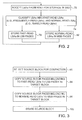
- Fig. 2 is a flow chart that schematically illustrates a method for data storage in SSD 24, in accordance with an embodiment of the present invention. The method begins with SSD controller 36 accepting LBAs for storage from host 28 via host interface 40, at an input step 70.
- Classification unit 56 in the SSD controller classifies the accepted LBAs, at a classification step 74.
- Unit 56 classifies the LBAs into a fast-access class of LBAs that are to be accessed with small access time (e.g., frequently-read LBAs), and a normal-access class of LBAs that are to be accessed with normal access time (e.g., rarely-read LBAs).
- Unit 56 provides the LBAs in the fast-access class to LSB write FIFO 64, and the LBAs in the normal-access class to MSB write FIFO 60.
- SSD controller 36 stores the LBAs buffered in LSB write FIFO 64 (e.g., frequently-read LBAs) in LSB pages of memory devices 32, at an LSB storage step 78.
- the SSD controller stores the LBAs buffered in MSB write FIFO 60 (e.g., rarely-read LBAs) in MSB pages of the memory devices, at an MSB storage step 82.
- the SSD controller programs a given group of memory cells (e.g., a row in a given block) by reading an entry from the LSB write FIFO and an entry from the MSB write FIFO, and storing the entries in the LSB page and the MSB page of the cell group, respectively. If one of the write FIFOs is empty, the SSD controller may store two entries from the other write FIFO in the LSB page and the MSB page of the cell group.
- the method then loops back to step 70 above in which the SSD accepts subsequent LBAs from the host.
- the classification of LBAs into the normal-access and fast-access classes is fixed, i.e., a pre-configured classification that does not change over time.
- unit 56 may be pre-configured with ranges of LBAs that are accessed frequently and other ranges of LBAs that are accessed rarely, and classify the accepted LBAs based on these ranges.
- This implementation is relatively simple and can be used, for example, with operating systems that store management data (that is accessed frequently) in predefined LBA ranges (e.g., at the low end of the LBA space).
- SSD controller 36 may be notified of the classification by host 28, over the interface between them.
- the host may indicate to the SSD controller which LBA ranges are accessed frequently and which LBA ranges are accessed rarely. Indications of this sort may be provided to the SSD controller in advance, or together with each LBA that is sent for storage in the SSD.
- Some storage protocols support commands that enable the host to provide such indications to the SSD.
- host 28 and SSD controller 36 communicate using the NVM Express protocol that is specified, for example, in "NVM Express," revision 1.0b, July 12, 2011, which is incorporated herein by reference.
- the NVM Express protocol specifies a Dataset Management (DSM) command, which is used by the host to indicate attributes for ranges of logical blocks.
- the attributes may comprise, for example, the frequency with which data is read or written and/or requested access latency for the data. See, for example, sections 6.6 and 6.8 and Figure 121 of the NVM Express specification, cited above.
- unit 56 classifies the accepted LBAs based on the attributes provided in the DSM command.
- the host may use the DSM command to specify the LBA range to be used as the computer's hibernation space.
- Unit 56 may optimize this LBA range for fast readout by storing the LBAs in this range in LSB pages. This technique reduces the computer wake-up time from hibernation.
- classification that is based on host notification is also relatively simple to implement but offers higher flexibility.
- This implementation can also be advantageous, for example, with operating systems that store management data in predefined LBA ranges (e.g., at the low end of the LBA space).
- processor 48 of SSD 24 determines the classification of LBAs adaptively and autonomously, irrespective of notifications from the host.
- processor 48 tracks the statistics of memory access (e.g., readout) operations performed on the various LBAs, and defines the classification accordingly.
- processor 48 may apply any suitable technique for automatically distinguishing between frequently-accessed and rarely-accessed LBAs, and then map the LBAs to the fast-access and normal-access classes accordingly.
- this functionality is embedded in the Flash Translation Layer (FTL) implemented in processor 48. This dynamic mapping may be combined with the fixed or host-assisted methods described above.
- FTL Flash Translation Layer
- processor 48 maintains for each LBA or LBA range a respective read counter, and increments the counter for each read operation from the LBA or LBA range.
- the counters may have any desired number of bits, i.e., any desired resolution or size.
- the counter of each LBA (or range) is stored as part of the entry of that LBA (or range) in the logical-to-physical address mapping.
- the logical-to-physical address mapping, including the counters may be stored, for example, in DRAM 52.
- processor 48 classifies the LBAs based on their read counter values. For example, processor 48 may classify in the fast-access class the LBAs whose counter values exceed a certain threshold, and classify in the normal-access class the LBAs whose counter values are below the threshold. As a result, the frequently-accessed LBAs will be stored in LSB pages and the rarely-accessed LBAs will be stored in MSB pages.
- processor 48 of SSD controller 36 carries out a compaction, or "garbage collection" process.
- This background process selects one or more memory blocks (referred to as source blocks) for compaction, copies the valid data from the selected source blocks to other storage locations in one or more other blocks (referred to as target blocks), and then erases the source blocks. The erased blocks are then ready for subsequent programming.
- SSD controller 36 (e.g., processor 48 and/or unit 56) stores the data belonging to the fast-access class in LSB pages and the data belonging to the normal-access class in MSB pages as part of the compaction process. For example, when using the read counters described above, processor 48 initially resets the read counters. During data readout, processor 48 increments the read counters of the various LBAs.
- processor 48 copies pages that belong to LBAs having high counter values to LSB pages in the target blocks, and copies pages that belong to LBAs having low counter values to MSB pages in the target blocks. After copying the pages, the read counters may be reset.
- processor 48 assigns to each block a respective readout grade that is indicative of:
- the readout grade of a block may be defined, for example, as the total number of readout operations of LSB pages from the block, minus the total number of readout operations of MSB pages from the block. Alternatively, any other suitable readout grade definition that meets the above guidelines can be used.
- processor 48 assigns blocks having low grades high priority when selecting candidate blocks for compaction.
- the grade-based criterion may be combined with other selection criteria, such as the number of "holes" (regions of invalid data) or the number of invalid pages in the block.
- Fig. 3 is a flow chart that schematically illustrates a method for memory block compaction, in accordance with an embodiment of the present invention.
- the method begins with processor 48 of SSD controller 36 selecting a source block for compaction, at a candidate selection step 90.
- Processor 48 may select the source block, for example, based on the readout grade assigned to the block, as explained above.
- Processor 48 copies the valid pages from the selected source block to a target block.
- the processor copies pages of the source block that belong to the fast-access class to LSB pages in the target block, at an LSB copying step 94. Pages of the source block that belong to the normal-access class are copied to MSB pages in the target block, at an MSB copying step 98.
- Processor 48 then erases the source block, at an erasure step 102.
- the example above refers to a compaction process that copies data from a single source block to a single target block.
- the compaction process may copy data jointly from any desired number of source blocks to any desired number of target blocks. Increasing the number of source blocks may improve the compaction efficiency.
- the fast-access storage configuration may comprise storing the data (e.g., LBA) in a small number of physical pages (e.g., in a single physical page), and the normal-access storage configuration may comprise splitting the data over a larger number of physical pages.
Landscapes
- Engineering & Computer Science (AREA)
- Theoretical Computer Science (AREA)
- Physics & Mathematics (AREA)
- General Engineering & Computer Science (AREA)
- General Physics & Mathematics (AREA)
- Human Computer Interaction (AREA)
- Computer Security & Cryptography (AREA)
- Read Only Memory (AREA)
- Information Retrieval, Db Structures And Fs Structures Therefor (AREA)
- Memory System (AREA)
Priority Applications (1)
| Application Number | Priority Date | Filing Date | Title |
|---|---|---|---|
| EP20162061.4A EP3686742A1 (de) | 2011-05-15 | 2012-05-14 | Selektive datenspeicherung auf lsb- und msb-seiten |
Applications Claiming Priority (2)
| Application Number | Priority Date | Filing Date | Title |
|---|---|---|---|
| US201161486284P | 2011-05-15 | 2011-05-15 | |
| US13/426,799 US8782370B2 (en) | 2011-05-15 | 2012-03-22 | Selective data storage in LSB and MSB pages |
Related Child Applications (1)
| Application Number | Title | Priority Date | Filing Date |
|---|---|---|---|
| EP20162061.4A Division EP3686742A1 (de) | 2011-05-15 | 2012-05-14 | Selektive datenspeicherung auf lsb- und msb-seiten |
Publications (2)
| Publication Number | Publication Date |
|---|---|
| EP2525293A1 true EP2525293A1 (de) | 2012-11-21 |
| EP2525293B1 EP2525293B1 (de) | 2020-03-11 |
Family
ID=46178419
Family Applications (2)
| Application Number | Title | Priority Date | Filing Date |
|---|---|---|---|
| EP20162061.4A Withdrawn EP3686742A1 (de) | 2011-05-15 | 2012-05-14 | Selektive datenspeicherung auf lsb- und msb-seiten |
| EP12167837.9A Active EP2525293B1 (de) | 2011-05-15 | 2012-05-14 | Selektive Datenspeicherung auf LSB- und MSB-Seiten von mehrstufigen Flash-Speichervorrichtungen |
Family Applications Before (1)
| Application Number | Title | Priority Date | Filing Date |
|---|---|---|---|
| EP20162061.4A Withdrawn EP3686742A1 (de) | 2011-05-15 | 2012-05-14 | Selektive datenspeicherung auf lsb- und msb-seiten |
Country Status (7)
| Country | Link |
|---|---|
| US (2) | US8782370B2 (de) |
| EP (2) | EP3686742A1 (de) |
| JP (1) | JP5907255B2 (de) |
| KR (1) | KR101388410B1 (de) |
| CN (1) | CN103608782B (de) |
| TW (1) | TWI460590B (de) |
| WO (1) | WO2013005118A1 (de) |
Cited By (4)
| Publication number | Priority date | Publication date | Assignee | Title |
|---|---|---|---|---|
| EP2929425A1 (de) * | 2012-12-04 | 2015-10-14 | Apple Inc. | Hinweise auf gelöschte daten von einer host- zu einer speichervorrichtung |
| EP3458963A4 (de) * | 2016-07-22 | 2020-02-12 | Pure Storage, Inc. | Optimierte datenschutzgestaltung auf der grundlage von verteiltem flash-nutzungsausgleich |
| WO2021061195A1 (en) * | 2019-09-24 | 2021-04-01 | Western Digital Technologies, Inc. | Initial data placement in hybrid object storage system |
| EP4020154A4 (de) * | 2019-08-28 | 2022-10-26 | Huawei Technologies Co., Ltd. | Datenspeicherverfahren und -vorrichtung |
Families Citing this family (46)
| Publication number | Priority date | Publication date | Assignee | Title |
|---|---|---|---|---|
| US9058281B2 (en) * | 2012-06-01 | 2015-06-16 | Seagate Technology Llc | Allocating memory usage based on quality metrics |
| US9081664B2 (en) * | 2012-08-10 | 2015-07-14 | Kabushiki Kaisha Toshiba | Memory system capable of preventing data destruction |
| US9361167B2 (en) * | 2012-10-24 | 2016-06-07 | SanDisk Technologies, Inc. | Bit error rate estimation for wear leveling and for block selection based on data type |
| CN103853665B (zh) * | 2012-12-03 | 2017-06-06 | 华为技术有限公司 | 存储空间分配方法及设备 |
| CN103077121B (zh) * | 2013-01-07 | 2016-01-27 | 深圳市江波龙电子有限公司 | 一种闪存存储设备中数据管理的方法及装置 |
| TWI498812B (zh) * | 2013-01-07 | 2015-09-01 | Mstar Semiconductor Inc | 資料存取方法以及使用此資料存取方法的電子裝置 |
| KR102068342B1 (ko) * | 2013-03-07 | 2020-01-20 | 삼성전자주식회사 | 메모리 제어기 및 그것을 포함하는 메모리 시스템 |
| CN103164344B (zh) * | 2013-03-12 | 2015-09-16 | 深圳市江波龙电子有限公司 | 一种闪存存储设备中数据管理的方法及装置 |
| CN103246615B (zh) * | 2013-04-24 | 2015-09-16 | 深圳市江波龙电子有限公司 | 一种闪存存储设备中数据管理的方法及装置 |
| WO2014209234A1 (en) * | 2013-06-26 | 2014-12-31 | Agency For Science, Technology And Research | Method and apparatus for hot data region optimized dynamic management |
| US9298389B2 (en) * | 2013-10-28 | 2016-03-29 | Lenovo Enterprise Solutions (Singapore) Pte. Ltd. | Operating a memory management controller |
| US9330015B2 (en) * | 2014-06-11 | 2016-05-03 | Vmware, Inc. | Identification of low-activity large memory pages |
| US9501422B2 (en) | 2014-06-11 | 2016-11-22 | Vmware, Inc. | Identification of low-activity large memory pages |
| US9563367B2 (en) | 2014-08-26 | 2017-02-07 | HGST Netherlands B.V. | Latency command processing for solid state drive interface protocol |
| CN105980992B (zh) | 2014-12-05 | 2018-02-13 | 华为技术有限公司 | 一种存储系统、识别数据块稳定性的方法以及装置 |
| CN104503707B (zh) * | 2014-12-24 | 2018-03-06 | 华为技术有限公司 | 读取数据的方法以及装置 |
| JP6320322B2 (ja) * | 2014-12-29 | 2018-05-09 | 東芝メモリ株式会社 | キャッシュメモリ装置及びプログラム |
| KR20160150384A (ko) * | 2015-06-22 | 2016-12-30 | 에스케이하이닉스 주식회사 | 데이터 저장 장치 및 그것의 동작 방법 |
| KR20170001237A (ko) * | 2015-06-26 | 2017-01-04 | 에스케이하이닉스 주식회사 | 상태 읽기를 수행하는 메모리 시스템 및 그것의 동작 방법 |
| US20170139826A1 (en) * | 2015-11-17 | 2017-05-18 | Kabushiki Kaisha Toshiba | Memory system, memory control device, and memory control method |
| KR20170099437A (ko) * | 2016-02-23 | 2017-09-01 | 에스케이하이닉스 주식회사 | 메모리 시스템 및 이의 동작 방법 |
| KR102553170B1 (ko) * | 2016-06-08 | 2023-07-10 | 에스케이하이닉스 주식회사 | 메모리 시스템 및 메모리 시스템의 동작 방법 |
| US10783146B2 (en) | 2016-07-19 | 2020-09-22 | Sap Se | Join operations in hybrid main memory systems |
| US10540098B2 (en) | 2016-07-19 | 2020-01-21 | Sap Se | Workload-aware page management for in-memory databases in hybrid main memory systems |
| US10437798B2 (en) | 2016-07-19 | 2019-10-08 | Sap Se | Full system simulator and memory-aware splay tree for in-memory databases in hybrid memory systems |
| US10698732B2 (en) * | 2016-07-19 | 2020-06-30 | Sap Se | Page ranking in operating system virtual pages in hybrid memory systems |
| US11977484B2 (en) | 2016-07-19 | 2024-05-07 | Sap Se | Adapting in-memory database in hybrid memory systems and operating system interface |
| US10452539B2 (en) | 2016-07-19 | 2019-10-22 | Sap Se | Simulator for enterprise-scale simulations on hybrid main memory systems |
| US10387127B2 (en) | 2016-07-19 | 2019-08-20 | Sap Se | Detecting sequential access data and random access data for placement on hybrid main memory for in-memory databases |
| US10474557B2 (en) | 2016-07-19 | 2019-11-12 | Sap Se | Source code profiling for line-level latency and energy consumption estimation |
| CN108170367B (zh) * | 2016-12-07 | 2021-04-20 | 瑞昱半导体股份有限公司 | 内存控制电路及其方法 |
| JP2018160194A (ja) | 2017-03-23 | 2018-10-11 | 東芝メモリ株式会社 | メモリシステムおよび方法 |
| US11010379B2 (en) | 2017-08-15 | 2021-05-18 | Sap Se | Increasing performance of in-memory databases using re-ordered query execution plans |
| US10754578B2 (en) * | 2018-05-09 | 2020-08-25 | Micron Technology, Inc. | Memory buffer management and bypass |
| US10942854B2 (en) | 2018-05-09 | 2021-03-09 | Micron Technology, Inc. | Prefetch management for memory |
| US10714159B2 (en) | 2018-05-09 | 2020-07-14 | Micron Technology, Inc. | Indication in memory system or sub-system of latency associated with performing an access command |
| US11010092B2 (en) | 2018-05-09 | 2021-05-18 | Micron Technology, Inc. | Prefetch signaling in memory system or sub-system |
| US11340810B2 (en) * | 2018-10-09 | 2022-05-24 | Western Digital Technologies, Inc. | Optimizing data storage device operation by grouping logical block addresses and/or physical block addresses using hints |
| CN109947678B (zh) * | 2019-03-26 | 2021-07-16 | 联想(北京)有限公司 | 一种存储装置、电子设备及数据交互方法 |
| KR102749204B1 (ko) | 2019-04-22 | 2025-01-06 | 삼성전자주식회사 | 상이한 동작 모드들에서 동작하는 뱅크들을 포함하는 불휘발성 메모리 장치, 메모리 컨트롤러의 동작 방법, 및 불휘발성 메모리 장치 및 메모리 컨트롤러를 포함하는 저장 장치 |
| WO2021035555A1 (zh) * | 2019-08-27 | 2021-03-04 | 华为技术有限公司 | 一种固态硬盘的数据存储方法、装置及固态硬盘ssd |
| CN111258505B (zh) * | 2020-01-21 | 2023-09-26 | 合肥兆芯电子有限公司 | 快闪存储器的数据合并方法、控制电路单元与存储装置 |
| US20210382818A1 (en) * | 2020-06-08 | 2021-12-09 | Western Digital Technologies, Inc. | Solid-State Storage Devices that Reduce Read Time for Read Time-Sensitive Data |
| US11366774B2 (en) * | 2020-09-24 | 2022-06-21 | Adesto Technologies Corporation | Memory latency reduction in XIP mode |
| CN112860185B (zh) * | 2021-01-29 | 2022-11-25 | 西藏宁算科技集团有限公司 | 基于lru算法的高可用缓存方法、存储装置以及电子设备 |
| JP7516300B2 (ja) * | 2021-03-17 | 2024-07-16 | キオクシア株式会社 | メモリシステム |
Citations (4)
| Publication number | Priority date | Publication date | Assignee | Title |
|---|---|---|---|---|
| US20080235467A1 (en) * | 2007-03-23 | 2008-09-25 | Canon Kabushiki Kaisha | Memory management device and method, program, and memory management system |
| US20080291731A1 (en) * | 2007-05-21 | 2008-11-27 | Sandisk Il Ltd. | Methods For Optimizing Page Selection In Flash-Memory Devices |
| US20090049234A1 (en) | 2007-08-14 | 2009-02-19 | Samsung Electronics Co., Ltd. | Solid state memory (ssm), computer system including an ssm, and method of operating an ssm |
| US20110010489A1 (en) | 2009-07-09 | 2011-01-13 | Phison Electronics Corp. | Logical block management method for a flash memory and control circuit storage system using the same |
Family Cites Families (18)
| Publication number | Priority date | Publication date | Assignee | Title |
|---|---|---|---|---|
| WO2004025476A1 (en) | 2002-09-16 | 2004-03-25 | Tigi Corporation | Storage system architectures and multiple caching arrangements |
| US7352618B2 (en) * | 2004-12-15 | 2008-04-01 | Samsung Electronics Co., Ltd. | Multi-level cell memory device and associated read method |
| US7707379B2 (en) | 2006-07-13 | 2010-04-27 | International Business Machines Corporation | Dynamic latency map for memory optimization |
| US7707380B2 (en) | 2006-09-29 | 2010-04-27 | Qimonda Ag | Memories, method of storing data in memory and method of determining memory cell sector quality |
| KR100771521B1 (ko) * | 2006-10-30 | 2007-10-30 | 삼성전자주식회사 | 멀티 레벨 셀을 포함하는 플래시 메모리 장치 및 그것의데이터 쓰기 방법 |
| TWI375953B (en) * | 2008-02-21 | 2012-11-01 | Phison Electronics Corp | Data reading method for flash memory, controller and system therof |
| US8706951B2 (en) * | 2008-07-18 | 2014-04-22 | Marvell World Trade Ltd. | Selectively accessing faster or slower multi-level cell memory |
| JP4461187B1 (ja) * | 2008-12-24 | 2010-05-12 | 株式会社東芝 | 不揮発性半導体メモリドライブ装置、情報処理装置および不揮発性半導体メモリドライブ装置における記憶領域の管理方法 |
| US20100169602A1 (en) * | 2008-12-29 | 2010-07-01 | Jared E Hulbert | Method and Apparatus for Efficient Memory Placement |
| US8239613B2 (en) * | 2008-12-30 | 2012-08-07 | Intel Corporation | Hybrid memory device |
| TWI397071B (zh) | 2008-12-31 | 2013-05-21 | A Data Technology Co Ltd | 記憶體儲存裝置及其控制方法 |
| US8332578B2 (en) * | 2009-07-31 | 2012-12-11 | Intel Corporation | Method and system to improve the performance of a multi-level cell (MLC) NAND flash memory |
| US8438361B2 (en) * | 2010-03-10 | 2013-05-07 | Seagate Technology Llc | Logical block storage in a storage device |
| US9183134B2 (en) * | 2010-04-22 | 2015-11-10 | Seagate Technology Llc | Data segregation in a storage device |
| JP2012033002A (ja) * | 2010-07-30 | 2012-02-16 | Toshiba Corp | メモリ管理装置およびメモリ管理方法 |
| TWI451435B (zh) * | 2010-10-08 | 2014-09-01 | Phison Electronics Corp | 非揮發性記憶體儲存裝置、記憶體控制器與資料儲存方法 |
| US9569351B2 (en) * | 2010-10-25 | 2017-02-14 | Seagate Technology Llc | Storing corresponding data units in a common storage unit |
| US8874872B2 (en) * | 2011-01-21 | 2014-10-28 | Seagate Technology Llc | Garbage collection management in memories |
-
2012
- 2012-03-22 US US13/426,799 patent/US8782370B2/en active Active
- 2012-05-13 JP JP2014510916A patent/JP5907255B2/ja active Active
- 2012-05-13 WO PCT/IB2012/052376 patent/WO2013005118A1/en not_active Ceased
- 2012-05-13 CN CN201280023874.8A patent/CN103608782B/zh active Active
- 2012-05-14 EP EP20162061.4A patent/EP3686742A1/de not_active Withdrawn
- 2012-05-14 EP EP12167837.9A patent/EP2525293B1/de active Active
- 2012-05-15 TW TW101117261A patent/TWI460590B/zh active
- 2012-05-15 KR KR1020120051422A patent/KR101388410B1/ko active Active
-
2014
- 2014-07-14 US US14/330,234 patent/US8914600B2/en active Active
Patent Citations (4)
| Publication number | Priority date | Publication date | Assignee | Title |
|---|---|---|---|---|
| US20080235467A1 (en) * | 2007-03-23 | 2008-09-25 | Canon Kabushiki Kaisha | Memory management device and method, program, and memory management system |
| US20080291731A1 (en) * | 2007-05-21 | 2008-11-27 | Sandisk Il Ltd. | Methods For Optimizing Page Selection In Flash-Memory Devices |
| US20090049234A1 (en) | 2007-08-14 | 2009-02-19 | Samsung Electronics Co., Ltd. | Solid state memory (ssm), computer system including an ssm, and method of operating an ssm |
| US20110010489A1 (en) | 2009-07-09 | 2011-01-13 | Phison Electronics Corp. | Logical block management method for a flash memory and control circuit storage system using the same |
Cited By (6)
| Publication number | Priority date | Publication date | Assignee | Title |
|---|---|---|---|---|
| EP2929425A1 (de) * | 2012-12-04 | 2015-10-14 | Apple Inc. | Hinweise auf gelöschte daten von einer host- zu einer speichervorrichtung |
| EP3458963A4 (de) * | 2016-07-22 | 2020-02-12 | Pure Storage, Inc. | Optimierte datenschutzgestaltung auf der grundlage von verteiltem flash-nutzungsausgleich |
| EP4020154A4 (de) * | 2019-08-28 | 2022-10-26 | Huawei Technologies Co., Ltd. | Datenspeicherverfahren und -vorrichtung |
| US12189990B2 (en) | 2019-08-28 | 2025-01-07 | Huawei Technologies Co., Ltd. | Data storage method and apparatus |
| WO2021061195A1 (en) * | 2019-09-24 | 2021-04-01 | Western Digital Technologies, Inc. | Initial data placement in hybrid object storage system |
| US11231876B2 (en) | 2019-09-24 | 2022-01-25 | Western Digital Technologies, Inc. | Initial data placement in hybrid object storage system |
Also Published As
| Publication number | Publication date |
|---|---|
| CN103608782A (zh) | 2014-02-26 |
| WO2013005118A1 (en) | 2013-01-10 |
| CN103608782B (zh) | 2016-09-07 |
| US8914600B2 (en) | 2014-12-16 |
| KR101388410B1 (ko) | 2014-04-22 |
| EP3686742A1 (de) | 2020-07-29 |
| TWI460590B (zh) | 2014-11-11 |
| US20120290768A1 (en) | 2012-11-15 |
| JP5907255B2 (ja) | 2016-04-26 |
| KR20120127698A (ko) | 2012-11-23 |
| JP2014513848A (ja) | 2014-06-05 |
| US8782370B2 (en) | 2014-07-15 |
| US20140325172A1 (en) | 2014-10-30 |
| EP2525293B1 (de) | 2020-03-11 |
| TW201248405A (en) | 2012-12-01 |
Similar Documents
| Publication | Publication Date | Title |
|---|---|---|
| EP2525293B1 (de) | Selektive Datenspeicherung auf LSB- und MSB-Seiten von mehrstufigen Flash-Speichervorrichtungen | |
| US12164421B1 (en) | Storage device with erase units written using a common page offset | |
| KR102904679B1 (ko) | 메모리 시스템 및 그것의 동작방법 | |
| US11030094B2 (en) | Apparatus and method for performing garbage collection by predicting required time | |
| TWI647702B (zh) | 記憶體控制器、記憶體系統及於一記憶體中管理資料配置的方法 | |
| CN108475232B (zh) | 使用xcopy和多逻辑条带的优化的基于主机的垃圾收集策略的高效实现方式 | |
| US11249903B2 (en) | Memory system for garbage collection operation and operating method thereof | |
| EP2703995A1 (de) | Schnelle Ausführung von Spülbefehlen mit einem adaptiven Verdichtungsverhältnis | |
| US12504899B2 (en) | Storage device including nonvolatile memory device and operating method of storage device | |
| US20130073798A1 (en) | Flash memory device and data management method | |
| US20140095555A1 (en) | File management device and method for storage system | |
| Alsalibi et al. | A survey of techniques for architecting SLC/MLC/TLC hybrid Flash memory–based SSDs | |
| US12360696B2 (en) | Communication of data relocation information by storage device to host to improve system performance | |
| CN103294604A (zh) | 闪存器件和使用闪存器件的电子设备 | |
| US10901892B2 (en) | Locality grouping during garbage collection with flush of buffered write data upon completion of garbage collection operation | |
| Yong et al. | Design and implementation of virtual stream management for NAND flash-based storage | |
| US10698621B2 (en) | Block reuse for memory operations | |
| US11797183B1 (en) | Host assisted application grouping for efficient utilization of device resources | |
| KR20220159270A (ko) | 스토리지 장치 및 그 동작 방법 | |
| HK1178990A (en) | Selecitve data storage in lsb and msb pages of multi-level flash memory devices | |
| HK1178990B (en) | Selecitve data storage in lsb and msb pages of multi-level flash memory devices | |
| US20250123760A1 (en) | Smart Host Stream Release |
Legal Events
| Date | Code | Title | Description |
|---|---|---|---|
| PUAI | Public reference made under article 153(3) epc to a published international application that has entered the european phase |
Free format text: ORIGINAL CODE: 0009012 |
|
| 17P | Request for examination filed |
Effective date: 20120514 |
|
| AK | Designated contracting states |
Kind code of ref document: A1 Designated state(s): AL AT BE BG CH CY CZ DE DK EE ES FI FR GB GR HR HU IE IS IT LI LT LU LV MC MK MT NL NO PL PT RO RS SE SI SK SM TR |
|
| AX | Request for extension of the european patent |
Extension state: BA ME |
|
| REG | Reference to a national code |
Ref country code: HK Ref legal event code: DE Ref document number: 1178990 Country of ref document: HK |
|
| STAA | Information on the status of an ep patent application or granted ep patent |
Free format text: STATUS: EXAMINATION IS IN PROGRESS |
|
| 17Q | First examination report despatched |
Effective date: 20171023 |
|
| RAP1 | Party data changed (applicant data changed or rights of an application transferred) |
Owner name: APPLE INC. |
|
| GRAP | Despatch of communication of intention to grant a patent |
Free format text: ORIGINAL CODE: EPIDOSNIGR1 |
|
| STAA | Information on the status of an ep patent application or granted ep patent |
Free format text: STATUS: GRANT OF PATENT IS INTENDED |
|
| INTG | Intention to grant announced |
Effective date: 20190923 |
|
| GRAS | Grant fee paid |
Free format text: ORIGINAL CODE: EPIDOSNIGR3 |
|
| GRAA | (expected) grant |
Free format text: ORIGINAL CODE: 0009210 |
|
| STAA | Information on the status of an ep patent application or granted ep patent |
Free format text: STATUS: THE PATENT HAS BEEN GRANTED |
|
| AK | Designated contracting states |
Kind code of ref document: B1 Designated state(s): AL AT BE BG CH CY CZ DE DK EE ES FI FR GB GR HR HU IE IS IT LI LT LU LV MC MK MT NL NO PL PT RO RS SE SI SK SM TR |
|
| REG | Reference to a national code |
Ref country code: GB Ref legal event code: FG4D |
|
| REG | Reference to a national code |
Ref country code: CH Ref legal event code: EP |
|
| REG | Reference to a national code |
Ref country code: AT Ref legal event code: REF Ref document number: 1244025 Country of ref document: AT Kind code of ref document: T Effective date: 20200315 |
|
| REG | Reference to a national code |
Ref country code: IE Ref legal event code: FG4D |
|
| REG | Reference to a national code |
Ref country code: DE Ref legal event code: R096 Ref document number: 602012068347 Country of ref document: DE |
|
| PG25 | Lapsed in a contracting state [announced via postgrant information from national office to epo] |
Ref country code: NO Free format text: LAPSE BECAUSE OF FAILURE TO SUBMIT A TRANSLATION OF THE DESCRIPTION OR TO PAY THE FEE WITHIN THE PRESCRIBED TIME-LIMIT Effective date: 20200611 Ref country code: FI Free format text: LAPSE BECAUSE OF FAILURE TO SUBMIT A TRANSLATION OF THE DESCRIPTION OR TO PAY THE FEE WITHIN THE PRESCRIBED TIME-LIMIT Effective date: 20200311 Ref country code: RS Free format text: LAPSE BECAUSE OF FAILURE TO SUBMIT A TRANSLATION OF THE DESCRIPTION OR TO PAY THE FEE WITHIN THE PRESCRIBED TIME-LIMIT Effective date: 20200311 |
|
| REG | Reference to a national code |
Ref country code: NL Ref legal event code: MP Effective date: 20200311 |
|
| PG25 | Lapsed in a contracting state [announced via postgrant information from national office to epo] |
Ref country code: GR Free format text: LAPSE BECAUSE OF FAILURE TO SUBMIT A TRANSLATION OF THE DESCRIPTION OR TO PAY THE FEE WITHIN THE PRESCRIBED TIME-LIMIT Effective date: 20200612 Ref country code: BG Free format text: LAPSE BECAUSE OF FAILURE TO SUBMIT A TRANSLATION OF THE DESCRIPTION OR TO PAY THE FEE WITHIN THE PRESCRIBED TIME-LIMIT Effective date: 20200611 Ref country code: LV Free format text: LAPSE BECAUSE OF FAILURE TO SUBMIT A TRANSLATION OF THE DESCRIPTION OR TO PAY THE FEE WITHIN THE PRESCRIBED TIME-LIMIT Effective date: 20200311 Ref country code: SE Free format text: LAPSE BECAUSE OF FAILURE TO SUBMIT A TRANSLATION OF THE DESCRIPTION OR TO PAY THE FEE WITHIN THE PRESCRIBED TIME-LIMIT Effective date: 20200311 Ref country code: HR Free format text: LAPSE BECAUSE OF FAILURE TO SUBMIT A TRANSLATION OF THE DESCRIPTION OR TO PAY THE FEE WITHIN THE PRESCRIBED TIME-LIMIT Effective date: 20200311 |
|
| REG | Reference to a national code |
Ref country code: LT Ref legal event code: MG4D |
|
| PG25 | Lapsed in a contracting state [announced via postgrant information from national office to epo] |
Ref country code: NL Free format text: LAPSE BECAUSE OF FAILURE TO SUBMIT A TRANSLATION OF THE DESCRIPTION OR TO PAY THE FEE WITHIN THE PRESCRIBED TIME-LIMIT Effective date: 20200311 |
|
| PG25 | Lapsed in a contracting state [announced via postgrant information from national office to epo] |
Ref country code: PT Free format text: LAPSE BECAUSE OF FAILURE TO SUBMIT A TRANSLATION OF THE DESCRIPTION OR TO PAY THE FEE WITHIN THE PRESCRIBED TIME-LIMIT Effective date: 20200805 Ref country code: IS Free format text: LAPSE BECAUSE OF FAILURE TO SUBMIT A TRANSLATION OF THE DESCRIPTION OR TO PAY THE FEE WITHIN THE PRESCRIBED TIME-LIMIT Effective date: 20200711 Ref country code: SK Free format text: LAPSE BECAUSE OF FAILURE TO SUBMIT A TRANSLATION OF THE DESCRIPTION OR TO PAY THE FEE WITHIN THE PRESCRIBED TIME-LIMIT Effective date: 20200311 Ref country code: SM Free format text: LAPSE BECAUSE OF FAILURE TO SUBMIT A TRANSLATION OF THE DESCRIPTION OR TO PAY THE FEE WITHIN THE PRESCRIBED TIME-LIMIT Effective date: 20200311 Ref country code: EE Free format text: LAPSE BECAUSE OF FAILURE TO SUBMIT A TRANSLATION OF THE DESCRIPTION OR TO PAY THE FEE WITHIN THE PRESCRIBED TIME-LIMIT Effective date: 20200311 Ref country code: RO Free format text: LAPSE BECAUSE OF FAILURE TO SUBMIT A TRANSLATION OF THE DESCRIPTION OR TO PAY THE FEE WITHIN THE PRESCRIBED TIME-LIMIT Effective date: 20200311 Ref country code: LT Free format text: LAPSE BECAUSE OF FAILURE TO SUBMIT A TRANSLATION OF THE DESCRIPTION OR TO PAY THE FEE WITHIN THE PRESCRIBED TIME-LIMIT Effective date: 20200311 Ref country code: CZ Free format text: LAPSE BECAUSE OF FAILURE TO SUBMIT A TRANSLATION OF THE DESCRIPTION OR TO PAY THE FEE WITHIN THE PRESCRIBED TIME-LIMIT Effective date: 20200311 |
|
| REG | Reference to a national code |
Ref country code: AT Ref legal event code: MK05 Ref document number: 1244025 Country of ref document: AT Kind code of ref document: T Effective date: 20200311 |
|
| REG | Reference to a national code |
Ref country code: DE Ref legal event code: R097 Ref document number: 602012068347 Country of ref document: DE |
|
| PLBE | No opposition filed within time limit |
Free format text: ORIGINAL CODE: 0009261 |
|
| STAA | Information on the status of an ep patent application or granted ep patent |
Free format text: STATUS: NO OPPOSITION FILED WITHIN TIME LIMIT |
|
| PG25 | Lapsed in a contracting state [announced via postgrant information from national office to epo] |
Ref country code: AT Free format text: LAPSE BECAUSE OF FAILURE TO SUBMIT A TRANSLATION OF THE DESCRIPTION OR TO PAY THE FEE WITHIN THE PRESCRIBED TIME-LIMIT Effective date: 20200311 Ref country code: DK Free format text: LAPSE BECAUSE OF FAILURE TO SUBMIT A TRANSLATION OF THE DESCRIPTION OR TO PAY THE FEE WITHIN THE PRESCRIBED TIME-LIMIT Effective date: 20200311 Ref country code: IT Free format text: LAPSE BECAUSE OF FAILURE TO SUBMIT A TRANSLATION OF THE DESCRIPTION OR TO PAY THE FEE WITHIN THE PRESCRIBED TIME-LIMIT Effective date: 20200311 Ref country code: MC Free format text: LAPSE BECAUSE OF FAILURE TO SUBMIT A TRANSLATION OF THE DESCRIPTION OR TO PAY THE FEE WITHIN THE PRESCRIBED TIME-LIMIT Effective date: 20200311 Ref country code: LI Free format text: LAPSE BECAUSE OF NON-PAYMENT OF DUE FEES Effective date: 20200531 Ref country code: CH Free format text: LAPSE BECAUSE OF NON-PAYMENT OF DUE FEES Effective date: 20200531 Ref country code: ES Free format text: LAPSE BECAUSE OF FAILURE TO SUBMIT A TRANSLATION OF THE DESCRIPTION OR TO PAY THE FEE WITHIN THE PRESCRIBED TIME-LIMIT Effective date: 20200311 |
|
| 26N | No opposition filed |
Effective date: 20201214 |
|
| PG25 | Lapsed in a contracting state [announced via postgrant information from national office to epo] |
Ref country code: PL Free format text: LAPSE BECAUSE OF FAILURE TO SUBMIT A TRANSLATION OF THE DESCRIPTION OR TO PAY THE FEE WITHIN THE PRESCRIBED TIME-LIMIT Effective date: 20200311 Ref country code: SI Free format text: LAPSE BECAUSE OF FAILURE TO SUBMIT A TRANSLATION OF THE DESCRIPTION OR TO PAY THE FEE WITHIN THE PRESCRIBED TIME-LIMIT Effective date: 20200311 |
|
| REG | Reference to a national code |
Ref country code: BE Ref legal event code: MM Effective date: 20200531 |
|
| GBPC | Gb: european patent ceased through non-payment of renewal fee |
Effective date: 20200611 |
|
| PG25 | Lapsed in a contracting state [announced via postgrant information from national office to epo] |
Ref country code: LU Free format text: LAPSE BECAUSE OF NON-PAYMENT OF DUE FEES Effective date: 20200514 |
|
| PG25 | Lapsed in a contracting state [announced via postgrant information from national office to epo] |
Ref country code: FR Free format text: LAPSE BECAUSE OF NON-PAYMENT OF DUE FEES Effective date: 20200531 Ref country code: GB Free format text: LAPSE BECAUSE OF NON-PAYMENT OF DUE FEES Effective date: 20200611 Ref country code: IE Free format text: LAPSE BECAUSE OF NON-PAYMENT OF DUE FEES Effective date: 20200514 |
|
| PG25 | Lapsed in a contracting state [announced via postgrant information from national office to epo] |
Ref country code: BE Free format text: LAPSE BECAUSE OF NON-PAYMENT OF DUE FEES Effective date: 20200531 |
|
| PG25 | Lapsed in a contracting state [announced via postgrant information from national office to epo] |
Ref country code: TR Free format text: LAPSE BECAUSE OF FAILURE TO SUBMIT A TRANSLATION OF THE DESCRIPTION OR TO PAY THE FEE WITHIN THE PRESCRIBED TIME-LIMIT Effective date: 20200311 Ref country code: MT Free format text: LAPSE BECAUSE OF FAILURE TO SUBMIT A TRANSLATION OF THE DESCRIPTION OR TO PAY THE FEE WITHIN THE PRESCRIBED TIME-LIMIT Effective date: 20200311 Ref country code: CY Free format text: LAPSE BECAUSE OF FAILURE TO SUBMIT A TRANSLATION OF THE DESCRIPTION OR TO PAY THE FEE WITHIN THE PRESCRIBED TIME-LIMIT Effective date: 20200311 |
|
| PG25 | Lapsed in a contracting state [announced via postgrant information from national office to epo] |
Ref country code: MK Free format text: LAPSE BECAUSE OF FAILURE TO SUBMIT A TRANSLATION OF THE DESCRIPTION OR TO PAY THE FEE WITHIN THE PRESCRIBED TIME-LIMIT Effective date: 20200311 Ref country code: AL Free format text: LAPSE BECAUSE OF FAILURE TO SUBMIT A TRANSLATION OF THE DESCRIPTION OR TO PAY THE FEE WITHIN THE PRESCRIBED TIME-LIMIT Effective date: 20200311 |
|
| P01 | Opt-out of the competence of the unified patent court (upc) registered |
Effective date: 20230523 |
|
| PGFP | Annual fee paid to national office [announced via postgrant information from national office to epo] |
Ref country code: DE Payment date: 20250319 Year of fee payment: 14 |