EP2523228A2 - Light-emitting diode and method for manufacturing same - Google Patents
Light-emitting diode and method for manufacturing same Download PDFInfo
- Publication number
- EP2523228A2 EP2523228A2 EP11731878A EP11731878A EP2523228A2 EP 2523228 A2 EP2523228 A2 EP 2523228A2 EP 11731878 A EP11731878 A EP 11731878A EP 11731878 A EP11731878 A EP 11731878A EP 2523228 A2 EP2523228 A2 EP 2523228A2
- Authority
- EP
- European Patent Office
- Prior art keywords
- layer
- light emitting
- emitting diode
- type
- type contact
- Prior art date
- Legal status (The legal status is an assumption and is not a legal conclusion. Google has not performed a legal analysis and makes no representation as to the accuracy of the status listed.)
- Granted
Links
Images



Classifications
-
- H—ELECTRICITY
- H10—SEMICONDUCTOR DEVICES; ELECTRIC SOLID-STATE DEVICES NOT OTHERWISE PROVIDED FOR
- H10H—INORGANIC LIGHT-EMITTING SEMICONDUCTOR DEVICES HAVING POTENTIAL BARRIERS
- H10H20/00—Individual inorganic light-emitting semiconductor devices having potential barriers, e.g. light-emitting diodes [LED]
- H10H20/80—Constructional details
- H10H20/81—Bodies
- H10H20/811—Bodies having quantum effect structures or superlattices, e.g. tunnel junctions
- H10H20/812—Bodies having quantum effect structures or superlattices, e.g. tunnel junctions within the light-emitting regions, e.g. having quantum confinement structures
-
- H—ELECTRICITY
- H10—SEMICONDUCTOR DEVICES; ELECTRIC SOLID-STATE DEVICES NOT OTHERWISE PROVIDED FOR
- H10H—INORGANIC LIGHT-EMITTING SEMICONDUCTOR DEVICES HAVING POTENTIAL BARRIERS
- H10H20/00—Individual inorganic light-emitting semiconductor devices having potential barriers, e.g. light-emitting diodes [LED]
- H10H20/01—Manufacture or treatment
- H10H20/011—Manufacture or treatment of bodies, e.g. forming semiconductor layers
- H10H20/013—Manufacture or treatment of bodies, e.g. forming semiconductor layers having light-emitting regions comprising only Group III-V materials
- H10H20/0133—Manufacture or treatment of bodies, e.g. forming semiconductor layers having light-emitting regions comprising only Group III-V materials with a substrate not being Group III-V materials
- H10H20/01335—Manufacture or treatment of bodies, e.g. forming semiconductor layers having light-emitting regions comprising only Group III-V materials with a substrate not being Group III-V materials the light-emitting regions comprising nitride materials
-
- H—ELECTRICITY
- H10—SEMICONDUCTOR DEVICES; ELECTRIC SOLID-STATE DEVICES NOT OTHERWISE PROVIDED FOR
- H10H—INORGANIC LIGHT-EMITTING SEMICONDUCTOR DEVICES HAVING POTENTIAL BARRIERS
- H10H20/00—Individual inorganic light-emitting semiconductor devices having potential barriers, e.g. light-emitting diodes [LED]
- H10H20/80—Constructional details
- H10H20/81—Bodies
- H10H20/811—Bodies having quantum effect structures or superlattices, e.g. tunnel junctions
-
- H—ELECTRICITY
- H10—SEMICONDUCTOR DEVICES; ELECTRIC SOLID-STATE DEVICES NOT OTHERWISE PROVIDED FOR
- H10H—INORGANIC LIGHT-EMITTING SEMICONDUCTOR DEVICES HAVING POTENTIAL BARRIERS
- H10H20/00—Individual inorganic light-emitting semiconductor devices having potential barriers, e.g. light-emitting diodes [LED]
- H10H20/80—Constructional details
- H10H20/81—Bodies
- H10H20/8215—Bodies characterised by crystalline imperfections, e.g. dislocations; characterised by the distribution of dopants, e.g. delta-doping
-
- H—ELECTRICITY
- H10—SEMICONDUCTOR DEVICES; ELECTRIC SOLID-STATE DEVICES NOT OTHERWISE PROVIDED FOR
- H10H—INORGANIC LIGHT-EMITTING SEMICONDUCTOR DEVICES HAVING POTENTIAL BARRIERS
- H10H20/00—Individual inorganic light-emitting semiconductor devices having potential barriers, e.g. light-emitting diodes [LED]
- H10H20/80—Constructional details
- H10H20/81—Bodies
- H10H20/822—Materials of the light-emitting regions
- H10H20/824—Materials of the light-emitting regions comprising only Group III-V materials, e.g. GaP
-
- H—ELECTRICITY
- H10—SEMICONDUCTOR DEVICES; ELECTRIC SOLID-STATE DEVICES NOT OTHERWISE PROVIDED FOR
- H10H—INORGANIC LIGHT-EMITTING SEMICONDUCTOR DEVICES HAVING POTENTIAL BARRIERS
- H10H20/00—Individual inorganic light-emitting semiconductor devices having potential barriers, e.g. light-emitting diodes [LED]
- H10H20/80—Constructional details
- H10H20/81—Bodies
- H10H20/822—Materials of the light-emitting regions
- H10H20/824—Materials of the light-emitting regions comprising only Group III-V materials, e.g. GaP
- H10H20/825—Materials of the light-emitting regions comprising only Group III-V materials, e.g. GaP containing nitrogen, e.g. GaN
-
- H—ELECTRICITY
- H10—SEMICONDUCTOR DEVICES; ELECTRIC SOLID-STATE DEVICES NOT OTHERWISE PROVIDED FOR
- H10P—GENERIC PROCESSES OR APPARATUS FOR THE MANUFACTURE OR TREATMENT OF DEVICES COVERED BY CLASS H10
- H10P14/00—Formation of materials, e.g. in the shape of layers or pillars
- H10P14/20—Formation of materials, e.g. in the shape of layers or pillars of semiconductor materials
- H10P14/24—Formation of materials, e.g. in the shape of layers or pillars of semiconductor materials using chemical vapour deposition [CVD]
-
- H—ELECTRICITY
- H10—SEMICONDUCTOR DEVICES; ELECTRIC SOLID-STATE DEVICES NOT OTHERWISE PROVIDED FOR
- H10P—GENERIC PROCESSES OR APPARATUS FOR THE MANUFACTURE OR TREATMENT OF DEVICES COVERED BY CLASS H10
- H10P14/00—Formation of materials, e.g. in the shape of layers or pillars
- H10P14/20—Formation of materials, e.g. in the shape of layers or pillars of semiconductor materials
- H10P14/29—Formation of materials, e.g. in the shape of layers or pillars of semiconductor materials characterised by the substrates
- H10P14/2901—Materials
-
- H—ELECTRICITY
- H10—SEMICONDUCTOR DEVICES; ELECTRIC SOLID-STATE DEVICES NOT OTHERWISE PROVIDED FOR
- H10P—GENERIC PROCESSES OR APPARATUS FOR THE MANUFACTURE OR TREATMENT OF DEVICES COVERED BY CLASS H10
- H10P14/00—Formation of materials, e.g. in the shape of layers or pillars
- H10P14/20—Formation of materials, e.g. in the shape of layers or pillars of semiconductor materials
- H10P14/32—Formation of materials, e.g. in the shape of layers or pillars of semiconductor materials characterised by intermediate layers between substrates and deposited layers
- H10P14/3202—Materials thereof
- H10P14/3214—Materials thereof being Group IIIA-VA semiconductors
- H10P14/3216—Nitrides
-
- H—ELECTRICITY
- H10—SEMICONDUCTOR DEVICES; ELECTRIC SOLID-STATE DEVICES NOT OTHERWISE PROVIDED FOR
- H10P—GENERIC PROCESSES OR APPARATUS FOR THE MANUFACTURE OR TREATMENT OF DEVICES COVERED BY CLASS H10
- H10P14/00—Formation of materials, e.g. in the shape of layers or pillars
- H10P14/20—Formation of materials, e.g. in the shape of layers or pillars of semiconductor materials
- H10P14/32—Formation of materials, e.g. in the shape of layers or pillars of semiconductor materials characterised by intermediate layers between substrates and deposited layers
- H10P14/3242—Structure
- H10P14/3244—Layer structure
- H10P14/3248—Layer structure consisting of two layers
-
- H—ELECTRICITY
- H10—SEMICONDUCTOR DEVICES; ELECTRIC SOLID-STATE DEVICES NOT OTHERWISE PROVIDED FOR
- H10P—GENERIC PROCESSES OR APPARATUS FOR THE MANUFACTURE OR TREATMENT OF DEVICES COVERED BY CLASS H10
- H10P14/00—Formation of materials, e.g. in the shape of layers or pillars
- H10P14/20—Formation of materials, e.g. in the shape of layers or pillars of semiconductor materials
- H10P14/34—Deposited materials, e.g. layers
- H10P14/3402—Deposited materials, e.g. layers characterised by the chemical composition
- H10P14/3414—Deposited materials, e.g. layers characterised by the chemical composition being group IIIA-VIA materials
- H10P14/3416—Nitrides
-
- H—ELECTRICITY
- H10—SEMICONDUCTOR DEVICES; ELECTRIC SOLID-STATE DEVICES NOT OTHERWISE PROVIDED FOR
- H10P—GENERIC PROCESSES OR APPARATUS FOR THE MANUFACTURE OR TREATMENT OF DEVICES COVERED BY CLASS H10
- H10P14/00—Formation of materials, e.g. in the shape of layers or pillars
- H10P14/20—Formation of materials, e.g. in the shape of layers or pillars of semiconductor materials
- H10P14/34—Deposited materials, e.g. layers
- H10P14/3438—Doping during depositing
- H10P14/3441—Conductivity type
- H10P14/3442—N-type
Definitions
- the present invention relates to a light emitting diode and a method of fabricating the same, and more particularly, to a light emitting diode with improved electrostatic discharge characteristics and/or luminous efficiency and a method of fabricating the same.
- a gallium nitride-based semiconductor is a light source for a full-color display, a traffic signal lamp, a general lighting, and optical communication devices, which has been prevalently used for an ultraviolet, blue/green light emitting diode, a laser diode, or the like.
- the gallium nitride-based light emitting device may include an active layer having an InGaN-based multi-quantum well structure disposed between n-type and p-type gallium nitride semiconductor layers, and may generate and discharge light by recombination of electrons and holes in the quantum well layer in the active layer.
- FIG. 1 is a cross-sectional view for explaining a light emitting diode according to the related art.
- the light emitting diode includes a substrate 11, a low-temperature buffer layer or nuclear layer 13, an undoped GaN layer 15, an n-type contact layer 17, an active region 25, and a p type contact layer 27.
- the light emitting diode includes the active region 25 having the multi-quantum well structure disposed between the n-type contact layer 17 and the p-type contact layer 27, thereby making it possible to improve luminous efficiency. Further, the light emitting diode controls an In content of an InGaN well layer within the multi-quantum well structure, thereby making it possible to emit light of a desired wavelength.
- the n-type contact layer 17 generally has a doping concentration within the range of 1 ⁇ 10 18 / ⁇ 1 ⁇ 10 19 / and serves to supply electrons in the light emitting diode.
- the current spreading performance within the light emitting diode has a large effect on the luminous efficiency of the light emitting diode.
- current concentration may occur according to a size of an area and a position in which the n-electrode and p-electrode may contact the contact layers 17 and 27.
- the light emitting diode When high voltage such as electrostatic discharge is applied to the light emitting diode, the light emitting diode may be easily broken due to the current concentration.
- thread dislocations generated from the low-temperature buffer layer 13 are transferred to the undoped GaN layer 15, the n-type contact layer 17, the active region 25, and the p-type contact layer 27. Since current intensively flows through these thread dislocations, the electrostatic discharge characteristics are further deteriorated.
- the active region having the multi-quantum well structure is generally formed by alternately stacking the InGaN well layer and the InGaN barrier layer.
- the well layer is formed of a semiconductor layer having a smaller bandgap than that of the barrier layer and electrons and holes are recombined between the well layer.
- the barrier layers may be doped with Si in order to lower a driving voltage Vf.
- the Si doping may have a negative effect on the crystal quality of the active region.
- the active region having the multi-quantum well structure is relatively thick according to the doping of Si.
- Si is doped in the active region including In, crystal defects frequently occur on the surface of the active region and in the active region and a wavelength shift is easily generated due to a space charge separation generated by a polarized field.
- Electrons and holes do not stay long in the active layer region due to the thermal vibration according to thermal or Joule heating, thereby making it possible to cause the efficiency droop.
- the efficiency droop may be caused by the occurrence of the Auger recombination due to the increase in carrier concentration when high current is injected. Further, the efficiency degradation may be caused with the increase in non-recombination due to electron overflow during the application of high voltage and the efficiency droop may be caused with the nonraditive-recombination rate due to the defects in a semiconductor crystal.
- an AlGaN electron blocking layer may be formed on the active layer in order to prevent electrons from being discharged out the active layer.
- the internal field may be generated in the active layer and the electron blocking layer by spontaneous polarization and piezo polarization. Due to the internal field within the active layer and the electron blocking layer, the high voltage should be applied in order to pass electrons through the active layer having the multi-quantum well structure.
- a conduction band at an n side has a higher energy level than a conduction band at a p side, based on the center of the active layer and the energy level of the electron blocking layer is lowered, thereby increasing a leakage current.
- Al composition may increase within the electron blocking layer, which degrades the crystal quality.
- An object of the present invention is to provide a light emitting diode with improved electrostatic discharge characteristics.
- Another object of the present invention is to provide a light emitting diode with low current leakage.
- Another object of the present invention is to provide a method for manufacturing a light emitting diode with improved current spreading performance.
- Another object of the present invention is to provide a light emitting diode capable of lowering a driving voltage by reducing the generation of internal field.
- Another object of the present invention is to provide a light emitting diode capable of reducing efficiency droop.
- a light emitting diode including: an n-type contact layer doped with silicon; a p-type contact layer; an active region interposed between the n-type contact layer and the p-type contact layer; a superlattice layer interposed between the n-type contact layer and the active region; an undoped intermediate layer interposed between the superlattice layer and the n-type contact layer; and an electron reinforcing layer interposed between the undoped intermediate layer and the superlattice layer, wherein only the final layer of the superlattice layer closest to the active region is intentionally doped with silicon, and the silicon doping concentration of the final layer is higher than that of the n-type contact layer.
- Almost all layers of the superlattice layer disposed close to the active region may be not intentionally with silicon, thereby making it possible to reduce leakage current and the final layer closet to the active region may be doped with high-concentration silicon to prevent junction characteristics from being deteriorated, thereby making it possible to improve electrostatic discharge characteristics.
- the final layer of the superlattice layer may contact the active region.
- the electron reinforcing layer may be doped with silicon, and the silicon doping concentration of the electron reinforcing layer may be higher than that of the n-type contact layer. Further, the electron reinforcing layer may contact the superlattice layer.
- the electron reinforcing layer may be made of GaN, and the superlattice layer may formed by alternately stacking GaN and InGaN. At this time, the final layer of the superlattice layer may be made of GaN. Meanwhile, the silicon doping concentration of the final layer of the superlattice layer may be the same as that of the electron reinforcing layer.
- the n-type contact layer may include a GaN layer, and the undoped intermediate layer may be made of GaN.
- the undoped intermediate layer may have relative high specific resistance. Accordingly, the undoped intermediate layer may be disposed on the n-type contact layer, thereby making it possible to uniformly spread electrons within the n-type contact layer.
- a method of fabricating a light emitting diode including: forming a buffer layer on a substrate; forming an n-type contact layer doped with silicon on the buffer layer; forming an undoped intermediate layer on the n-type contact layer; forming an electron reinforcing layer on the undoped intermediate layer; forming a superlattice layer on the electron reinforcing layer; and forming an active region on the superlattice layer, wherein only the final layer of the superlattice layer is doped with silicon, and the silicon doping concentration of the final layer is higher than that of the n-type contact layer.
- the method of fabricating a light emitting diode may further include: growing the electron reinforcing layer of a gallium nitride-based semiconductor layer at a first temperature by supplying nitrogen source gas and metal source gas into a chamber; stopping the supply of the metal source gas and maintaining the grown n-side gallium nitride-based semiconductor layer on a substrate having the first temperature for a first time; lowering a temperature of the substrate to a second temperature after the first time elapses; and growing the superlattice layer at the second temperature by supplying the metal source gas into the chamber.
- the first time may be in a range of 3 minutes to 10 minutes.
- the method of fabricating a light emitting diode may further include: stopping the supply of the metal source gas after the active region is grown on the superlattice layer; raising the temperature of the substrate to a third temperature for a second time; and growing a p-type gallium nitride-based semiconductor layer on the active region at the third temperature.
- the second time may be in a range of 5 minutes to 15 minutes.
- the electron reinforcing layer may be maintained at a temperature suitable to grow the electron reinforcing layer or a temperature similar thereto for 1 hour before the growth temperature of the superlattice falls, such that the metal source gas remaining the chamber is discharged to the outside for 1 hour, thereby making it possible to prevent a nitride layer having a poor crystal quality from being generated on the electron reinforcing layer while the substrate temperature falls to the growth temperature of the superlattice layer. Further, the n-side gallium nitride semiconductor layer grown on the substrate is heat treated, thereby improving the crystal quality.
- a light emitting diode including: an n-type contact layer doped with silicon; a p-type contact layer; an active region interposed between the n-type contact layer and the p-type contact layer; a superlattice layer interposed between the n-type contact layer and the active region; an undoped intermediate layer interposed between the superlattice layer and the n-type contact layer; and an electron reinforcing layer interposed between the undoped intermediate layer and the superlattice layer, wherein the n-type contact layer has n-type GaN layers and n-type AlGaN layers interposed between the n-type GaN layers.
- the light emitting diode may further include: a substrate; a low-temperature buffer layer disposed on the substrate; and an undoped GaN layer interposed between the low-temperature buffer layer and the n-type contact layer.
- the n-type AlGaN layer is inserted between the n-type GaN layers to prevent the thread dislocations generated in the low-temperature buffer layer from being transferred to the active region, thereby making it possible to lower the leakage current and the electrostatic discharge characteristics.
- Only the final layer of the superlattice layer closest to the active region may be intentionally doped with silicon, and the silicon doping concentration of the final layer may be higher than that of the n-type contact layer. Almost all the layers of the superlattice layer disposed near the active region is not intentionally doped with silicon, thereby making it possible to reduce the leakage current and the final layer closest to the active region is doped with the high-concentration silicon to prevent the junction characteristics from being deteriorated, thereby making it possible to improve the electrostatic discharge characteristics. In particular, the final layer of the superlattice layer may contact the active region.
- the electron reinforcing layer may be doped with silicon.
- the silicon doping concentration of the electron reinforcing layer may be higher than that of the n-type contact layer.
- the electron reinforcing layer may contact the superlattice layer.
- the electron reinforcing layer may be made of GaN, and the superlattice layer may be formed by alternately stacking GaN and InGaN.
- the final layer of the superlattice layer may be made of GaN.
- the silicon doping concentration of the final layer of the superlattice layer may be the almost same as that of the electron reinforcing layer.
- the undoped intermediate layer may be made of GaN.
- the undoped intermediate layer may have relative high specific resistance. Accordingly, the undoped intermediate layer may be disposed on the n-type contact layer, thereby making it possible to uniformly spread electrons within the n-type contact layer.
- a light emitting diode including: an n-type contact layer; a p-type contact layer formed on the n-type contact layer; an active region having a multi-quantum well structure and interposed between the n-type contact layer and the p-type contact layer; and a spacer layer interposed between the n-type contact layer and the active region, wherein the spacer layer is doped with n-type impurities, and the n-type impurity doping concentration is relatively higher than the impurity doping concentration of the n-type contact layer, and the active region is undoped with the n-type impurities.
- the spacer layer may contains In, wherein the content of In is lower than that of In in a barrier layer of the active region and higher than that of In in a well layer.
- the active region may have a multi-quantum well structure including an InGaN layer.
- the spacer layer may include an InGaN layer, and may be formed by alternately stacking InxGa11-xN (0 ⁇ x ⁇ 1) and InyGa1-yN (0 ⁇ y ⁇ 1).
- the spacer layer may include mutually alternately stacked superlattice layers.
- the spacer layer may be configured of a plurality of layers, at least one layer adjacent to the active region of the plurality of layers being doped with n-type impurities, remaining layers thereof being undoped with the n-type impurities, and the n-type impurity doping concentration being relatively higher than the impurity doping concentration of the n-type contact layer.
- the light emitting diode may further include an intermediate layer formed between the spacer layer and the n-type contact layer, wherein the intermediate layer includes a layer doped with the n-type impurities at a concentration relatively higher than the impurity doping concentration of the n-type contact layer and relatively lower than the n-type impurity doping concentration of the spacer layer.
- the intermediate layer may include an n-type AlGaN layer.
- the n-type AlGaN layer may have gradually or stepwise reduced Al composition toward the active region.
- the n-type AlGaN layer may be formed in a multilayer film structure of AlGaN/GaN or AlGaN/InGaN.
- the intermediate layer may further include an n-GaN layer between the spacer layer and the n-type AlGaN layer.
- the intermediate layer may include at least one of an undoped GaN layer and a low-doped n-GaN layer between the n-type AlGaN layer and the n-type contact layer.
- the light emitting diode may further include a p-type clad layer formed between the active region and the p-type contact layer.
- the p-type clad layer may include a p-type AlGaN layer.
- the p-type AlGaN layer may be formed in a multilayer film structure of AlGaN/GaN or AlGaN/InGaN.
- a layer adjacent to the active region of the p-type AlGaN layers may be made of AlGaN.
- the AlGaN layer adjacent to the active region of the p-type AlGaN layers may be thinner than other layers within the p-type clad layer.
- the p-type AlGaN may have gradually or stepwise reduced Al composition toward the p-type contact layer.
- the light emitting diode may further include an InAlN layer formed between the active region and the p-type clad layer.
- the InAlN layer may be formed in a superlattice structure of InN/AlN.
- the InAlN layer may have an InN layer doped with p-type impurities in the superlattice structure of InN/AlN.
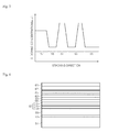
- FIG. 2 is a cross-sectional view for explaining a light emitting diode according to an exemplary embodiment of the present invention and FIG. 3 shows a schematic silicon doping profile of the light emitting diode.
- the light emitting diode is configured to include an n-type contact layer 57, an undoped intermediate layer 59, an electron reinforcing layer 61, a superlattice layer 63, an active region 65, and a p-type contact layer 69. Further, the light emitting diode may include a substrate 51, a low-temperature buffer layer or nuclear layer 53, a buffer layer 55, and a p-type clad layer 67.
- the substrate 51 is a substrate for growing a gallium nitride-based semiconductor layer.
- the substrate may be made of sapphire, SiC, spinel, or the like, but is not specifically limited.
- the substrate may be a patterned sapphire substrate (PSS).
- the nuclear layer 53 may be formed of (Al, Ga) N at a low temperature of 400 to 600 in order to grow the buffer layer 55 on the substrate 51.
- the nuclear layer 53 may be made of GaN or AlN.
- the nuclear layer may be formed to have a thickness of about 25 nm.
- the buffer layer 55 which is a layer to reduce the defect occurrence such as dislocations between the substrate 51 and the n-type contact layer 57, is grown at a relatively high temperature.
- the buffer layer 55 may be made of, for example, the undoped GaN.
- the n-type contact layer 57 is formed of an n-type impurity, for example, Si-doped gallium nitride semiconductor layer.
- the n-type contact layer 57 may include a GaN layer and may be formed of a single layer or a multi-layer. As shown in FIG. 4 , the n-type contact layer 57 may be configured to include an n-type first GaN layer 57a, an n-type AlGaN layer 57b, and an n-type second GaN layer 57c. That is, the AlGaN layer 57b is interposed between the GaN layers 57a and 57c.
- An Si doping concentration doped on the n-type contact layer may be in the range of 1 ⁇ 10 1g / ⁇ 1 ⁇ 10 19 / .
- the biaxial stress occurs by the n-type AlGaN layer 57b.
- the biaxial stress is reduced by the compression stress, thereby making it possible to reduce the thread dislocations due to the change in stress. Therefore, it is possible to prevent the thread dislocations transferred through the nuclear layer 53 and the high-temperature buffer layer 55 from being transferred to the active region 65 by disposing the n-type AlGaN layer 57b between the n-type GaN layers 57a and 57c.
- the undoped intermediate layer 59 may be made of the GaN, which is not intentionally doped with impurities, to have a thickness of 100 to 5000 . Since the undoped intermediate layer 59 is not doped with impurities, it has relatively higher specific resistance as compared to the n-type contact layer. Therefore, electrons introduced into the active layer 65 from the n-type contact layer 57 may be uniformly spread within the n-type contact layer 57 before passing through the undoped intermediate layer 59.
- the electron reinforcing layer 61 is formed on the undoped intermediate layer 59.
- the electron reinforcing layer 61 may be made of the GaN doped with Si at high concentration to have a thickness of 10 to 2000 , thereby making it possible to lower the forward voltage of the light emitting diode.
- the doping concentration of Si doped on the electron reinforcing layer 61 is higher than the silicon doping concentration of the n-type contact layer 57.
- the silicon doping concentration within the electron reinforcing layer 61 may be four times or higher than the silicon doping concentration of the n-type contact layer 57.
- the n-type contact layer 57, the undoped intermediate layer 59, and the electron reinforcing layer 61 may be continuously grown by supplying the metal source gas to the chamber.
- the metal source gas organic matters such as Al, Ga, and In, for example, TMA, TMG, and/or TMI, or the like, are used. These layers may be grown at a first temperature, for example, at 1050 ⁇ 1150.
- the superlattice layer 63 is formed on the electron reinforcing layer 61.
- the superlattice layer 63 may be formed by alternately stacking the GaN layer and the InGaN layer at a thickness of, for example, 20 .
- a first layer of the superlattice layer 63 may be made of GaN or InGaN, but the final layer may be made of GaN.
- the final layer of the superlattice layer 63 is doped with high-concentration Si. The doping concentration of Si doped on the final layer may be about four times to five times higher than the concentration of Si doped on the n-type contact layer 57.
- the Si concentration doped on the final layer of the superlattice layer 63 may be approximately the same as the doping concentration of the electron reinforcing layer 61. Therefore, the final layer of the superlattice layer 63 and the electron reinforcing layer 61 below the superlattice layer 63 are formed of a high-concentration doped layer and the remaining layers of the superlattice layer 63 positioned therebetween is formed of the undoped layer.
- the superlattice layer 63 Most layers of the superlattice layer 63 are formed of the undoped layer, thereby making it possible to reduce the leakage current of the light emitting diode. Further, the final layer of the superlattice layer 63 is doped at high concentration, thereby making it possible to improve junction characteristics between the superlattice layer 63 and the active region 65.
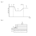
- the superlattice layer 63 may be grown at a relatively lower temperature that the electron reinforcing layer 61. As shown in FIG. 5 , before the superlattice layer 63 is grown, the electron reinforcing layer 61 is grown and then, the supply of metal source gas stops, and the grown electron reinforcing layer 61 is maintained on the substrate 21 of a first temperature T1 for a first time t1.
- the first time t1 may be a time of sufficiently discharge the metal source gas remaining in the chamber, that is, about 3 to 10 minutes, preferably, about 5 to 7 minutes.
- the n-type contact layer 57 and the intermediate layer 59 have been heat-treated, including the electron reinforcing layer 61, thereby improving the crystal quality of the n-side semiconductor layer.
- the second temperature T2 is set to a temperature suitable to grow the superlattice layer 63.
- the second temperature T2 may be in the range of, for example, 650 to 800 .
- the active region 65 is grown on the superlattice layer 63.
- the active region 65 may be grown at the same temperature as the superlattice layer 63 or relatively lower temperature than the superlattice layer 63, for example, 650 to 750 .
- FIG. 5 shows the case in which the active region 65 is grown at the growth temperature of the superlattice layer 63, i.e., the second temperature T2.
- the active region 65 may have the multi-quantum well structure in which the barrier layer and the InGaN quantum well layer are alternately stacked.
- the barrier layer may be formed of the gallium nitride semiconductor layer having a wider bandgap than that of the quantum well layer, for example, GaN, InGaN, AlGaN, or AlInGaN.
- the In composition ratio within the InGaN quantum well layer is determined by the desired optical wavelength.
- the active region 65 may contact the final layer of the superlattice layer 63.
- the barrier layer and the quantum well layer of the active region 65 may be formed of the undoped layer in which impurities are not doped, in order to improve the crystal quality of the active region or may be doped with impurities within some or entire active region in order to lower forward voltage.
- a p-type contact layer 69 is disposed on the active region 65 and a p-type clad layer 67 may be interposed between the active region 65 and the p-type contact layer 69.
- the supply of metal source gas stops and the temperature of the substrate 51 rises to a third temperature T3 for the second time t2.
- the second time t2 is set to a time in which the metal source gas remaining in the chamber can be sufficiently discharged.
- the second time t2 may be in the range of 5 to 15 minutes.
- the supply of metal source gas may stop and the temperature of the substrate 51 may be maintained at the active region growth temperature for the third time, for example, at the second temperature T2 for a third time.
- the third time may be, for example, in the range of the same time as the first time, i.e., 3 to 10 minutes.
- a unit maintaining the temperature at the second temperature for the third time and a unit increasing the temperature from the second temperature to the third temperature for the second time t2 may be used an alternative unit to each other, but is not limited thereto. These units may be used, complementing with each other.
- the metal source gas is supplied into the chamber and the p-side gallium nitride-based semiconductor layer, for example, the p-type clad layer 67 or the p-type contact layer 69 are grown, at the third temperature T3.
- the p-type clad layer 67 may be AlGaN.
- the p-type gallium nitride-based semiconductor layer 69 may be a multi-layer structure including a single layer or a GaN layer.
- the individual light emitting diode chips are manufactured by using the epitaxial layers.
- the epitaxial layer having the above-mentioned structure was grown with reference to FIGS. 2 and 3 by using a MOCVD device. In this case, all the other conditions were the same and the Si doping position was different at the GaN/InGaN superlattice layer.
- the n-type GaN contact layer 57, the undoped GaN intermediate layer 59, the high-concentration doped GaN electron reinforcing layer 61 were sequentially grown on the undoped GaN buffer layer 55, the superlattice layer was grown on the electron reinforcing layer 61, and the active region 65 having the multi-quantum well structure, the p-type AlGaN clad layer 67, and the p-type GaN contact layer 69 were sequentially grown on the superlattice layer.
- Comparative Example doped Si on all the GaN layers in the superlattice layer and Example doped only the final layer of the superlattice, i.e., the GaN layer with Si at the same high concentration as the electron reinforcing layer 61.
- the grown epitaxial layer was separated, together with the substrate and measures the optical characteristics and the electrical characteristics. The results were listed in Table 1.
- the electrostatic discharge (ESD) characteristics used the reverse voltage of 1000 V to perform the electrostatic discharge test on the good light emitting diodes manufactured on the same wafer to confirm the occurrence of defects, which are represented by the ESD pass ratio.
- the values measured before the ESD test was performed were represented by percentage based on Comparative Example.
- Example and Comparative Example according to the present invention slightly reduced the peak wavelength and slightly increased the forward voltage, so that the optical output was slightly reduced but the large difference was not shown.
- the epitaxial layer having a structure according to Example of FIG. 4 was grown by the MOCVD device. In this case, all the other conditions were the same.
- the case (Comparative Example) in which the n-type contact layer was formed only the n-type GaN was compared with the case (Example) in which the n-type AlGaN layer was interposed between the n-type GaN layers.
- the grown epitaxial layer was separated, together with the substrate and measured the optical characteristics and the electrical characteristics. The results were listed in Table 2. in this configuration, the electrostatic discharge (ESD) characteristics used the reverse voltage of 1000 V to perform the electrostatic discharge test on the good light emitting diodes manufactured on the same wafer to confirm the occurrence of defects, which were represented by the ESD pass ratio.
- the optical output and the leakage current were subjected to the ESD test and then, the values measured in the good light emitting diodes were represented by percentage, based on Comparative Example.
- Table 2 ESD Pass Ratio Peak Wavelength (nm) Optical Output Leakage Current @-5 V Comparative Example 69.34% 454.0 100 100 Example 87.68% 453.64 98.9 100
- Example according to the present invention shown the case in which the peak wavelength was slightly reduced and the optical output was slightly reduced, as compared to Comparative Example. However, Example shown the significantly improved ESD characteristics as compared to Comparative Example and the leakage current of the light emitting diodes passing through the ESD has no difference between Comparative Example and Example.
- FIG. 6 is a cross-sectional view for explaining a light emitting diode according to an exemplary embodiment of the present invention
- FIG. 7 shows a schematic silicon doping profile of the light emitting diode
- FIG. 8 shows a spacer layer structure of the light emitting diode.
- the light emitting diode includes a substrate 121, an n-type contact layer 126, a spacer layer 128, an active region 129 having a multi-quantum well structure, and a p-type contact layer 133.
- a nuclear layer 123 and an undoped GaN layer 125 may be interposed between the substrate 121 and the n-type contact layer 126.
- the substrate 121 is a substrate to grow the gallium nitride-based semiconductor layer.
- the substrate may be made of sapphire, SiC, spinel, or the like, but is not specifically limited.
- the substrate may be a patterned sapphire substrate (PSS).
- the nuclear layer 123 may be made of (Al, Ga)N at a low temperature of 400 to 600 in order to grow the u-GaN 125 on the substrate 121, preferably, AlN.
- the nuclear layer may be formed of a thickness of about 25 nm.
- the u-GaN layer 125 is a layer to reduce the occurrence of defects such as dislocations between the substrate 121 and the n-type contact layer 126 and is grown at relatively high temperature, for example, 900 to 1200 ..
- the n-type contact layer 126 is a layer on which the n-electrode 139 is formed and may be doped with n-type impurities such as Si or Ge.
- the impurity concentration of the n-type contact layer 126 may be, for example, 5 ⁇ 10 18 atm/ and may be an n-GaN grown at relatively high temperature, a first temperature T1, for example, 2 or less at 900 to 1200 .
- the spacer layer 128 may be made of a (Al, In, Ga) N-based III group nitride semiconductor layer having a smaller bandgap than that of the barrier layer of the active region 129 and a larger bandgap than that of the well layer.
- the spacer layer 128 may include In x Gal 1-x N(0 ⁇ x ⁇ 1).
- the spacer layer 128 is doped with an n-type impurity at high concentration, thereby lowering the forward voltage of the light emitting diode. As shown in FIG. 7 , the doping concentration of the n-type impurity doped on the spacer layer 128 is higher than the n-type impurity doping concentration of the n-type contact layer 126.
- the In composition ratio of the spacer layer 128 may be smaller than the In composition ratio within the InGaN quantum well layer. In this case, it can confine charges in the active region well, thereby making it possible to improve the luminous efficiency.
- the n-type impurity is doped in some thickness regions adjacent to the active region 129 based on the growth direction of the spacer layer 128.
- the remaining thickness regions other than thickness regions doped with the n-type impurity undope the n-type impurity.
- Only some thickness region adjacent to the active region 129 among the entire thickness regions of the spacer layer 128 is doped with the n-type impurity, so that electrons can be smoothly injected from the spacer layer 128 to the active region 129.
- the doping concentration in the area in which the n-type impurity is doped may be relatively higher than the impurity doping concentration of the n-type contact layer 126, for example, 9 ⁇ 10 19 atm/.
- the spacer layer 128 may have a structure in which (Al, In, Ga)N-based III group nitride semiconductor layers 128a and 128b having a smaller bandgap than that of the barrier layer of the active region 129 and a larger bandgap than that of the well layer are alternately stacked.
- the spacer layer 128 may be made by alternately stacking In x Gal 1-x N (0 ⁇ x ⁇ 1)128a and In y Ga 1-y N (0 ⁇ y ⁇ 1)128b having different compositions.
- the In x Gal 1-x N (0 ⁇ x ⁇ 1)28a may be formed at, for example, a thickness of 30 to 40 and the In y Ga 1-y N (0 ⁇ y ⁇ 1)28b may be formed at a thickness of 15 to 20 .
- the spacer layers 128 having a stacked structure of In x Gal 1-x N (0 ⁇ x ⁇ 1) 128a and InyGa 1- yN (0 ⁇ y ⁇ 1) 128b may improve the crystallinity of the active region 129 formed thereon and reduce strain.
- the spacer layers 128 may be formed at seven to fifteen periods. When it is below 7 periods, the spacer layers 128 are weak in terms of an effect of alleviating the strain generated in the active region, and when it exceeds 15 periods, process time is increased.
- the remaining layers other than the layers doped with the n-type impurities are undoped with the n-type impurities.
- Only an InGaN layer 128a and/or an InGaN layer 128b adjacent to the active region 129 of the spacer layers 128 are doped with the n-type impurities, thereby making it possible to smoothly inject electrons from the spacer layers 128 into the active region 129.
- the doping concentration of the InGaN layer 128a doped with the n-type impurities may be, for example, 9 ⁇ 10 19 atm/cm3, which is relatively higher than the impurity doping concentration of the n-type contact layer 126. Accordingly, the increase in resistance of the spacer layers 128 may be prevented, and the efficiency of injection of the electrons into the active region may be increased by the electron created in the spacer layers 128.
- Most layers of the spacer layers 128 are formed as undoped layers, thereby making it possible to reduce leakage current of the light emitting diode.
- the at least one layer 128a and 128b adjacent to the active region 129 are doped with the n-type impurities at a high concentration, thereby making it possible to improve junction characteristics between the spacer layer 128 and the active region 129.
- the spacer layer 128c adjacent to the active region 129 may be an InGaN layer further including In as compared to other semiconductor layers configuring the spacer layer 128.
- the amount of In included in the spacer layer 128c adjacent to the active region 129 may be higher than that in the quantum well layer.
- the n-type impurities are doped at about doping concentration of the n-type contact layer, and may be preferably doped toward the n-type contact layer 126 within the spacer layer 128c.
- the active region 129 has a multi-quantum well structure in which a barrier layer and a quantum well layer are alternately stacked, wherein the quantum well layer includes an InGaN layer.
- the quantum barrier layer may be made of a gallium nitride based semiconductor layer having a bandgap wider than that of the quantum well layer, for example, GaN, InGaN, AlGaN, or AlInGaN.
- An In composition ratio within the InGaN quantum well layer is determined by a desired optical wavelength.
- the active region 129 is undoped with the n-type impurities, for example, Si or Ge.
- a p-type contact layer 133 is disposed on the active region 129.
- the p-type contact layer 133 may be made of, for example, GaN on the active region 129.
- a transparent electrode such as Ni/Au or indium tin oxide (ITO) is formed on the p-type contact layer 133, and a p-electrode 134 may be formed thereon using a liftoff process.
- an n-electrode 135 such as Ti/Al, etc., may be formed on the n-type contact layer 126 using the liftoff process.
- the active region 129 has the quantum barrier layer and the quantum well layer undoped with the n-type impurities and is grown on the spacer layer 128 having the stacked structure of In x Gal 1-x N (0 ⁇ x ⁇ 1) 128a and InyGa 1-y N (0 ⁇ y ⁇ 1) 128b mostly not including the n-type impurities, thereby making it possible to improve the crystallinity of the active region 129 and reduce the strain.
- the InGaN layer 128a and/or the InGaN layer 128b adjacent to the active region 129 of the spacer layers 128 are doped with the n-type impurities to smoothly inject electrons from the spacer layer 128 into the active region 129, thereby making it possible to increase a recombination ratio of carriers in the active region 129. As a result, it is possible to improve light emitting efficiency of the light emitting diode.
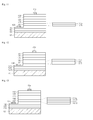
- FIGS. 9 and 10 each are cross-sectional views for explaining a light emitting diode according to another exemplary embodiment of the present invention and show a silicon doping profile.
- a light emitting diode according to the present embodiment has the almost same stacked structure as that of the light emitting diode described with reference to FIGS. 6 to 8 ; however, it further includes an intermediate layer 127 doped with n-type impurities between the spacer layer 128 and the n-type contact layer 126 and a p-type clad layer 131 interposed between the active region 129 and the p-type contact layer 133.
- the intermediate layer 127 is doped with the n-type impurities at, for example, a concentration of 2.5 ⁇ 10 19 atm/cm3, which is relatively higher than the impurity doping concentration of the n-type contact layer 126 and is relative lower than the n-type impurity doping concentration of the spacer layer 128, and may include an n-AlGaN layer, as shown in FIG. 10 .
- the n-AlGaN layer may have gradually or stepwise reduced Al composition toward the active region 129.
- Al has a composition range of 10 to 15% and is stacked at a thickness of 10 to 100nm, preferably, 30 to 60nm.
- the Al composition is gradually or stepwise reduced within the n-AlGaN layer, such that the intermediate layer 127 has a gradually reduced energy level toward the active region 129. Therefore, the intermediate layer 127 may have the lowest energy level at the interface between the intermediate layer 127 and the spacer layer 128.
- the n-AlGaN layer may be formed in a multi-layer film structure.
- n-AlGaN layer may be configured of a multi-layer film of AlGaN/GaN or AlGaN/InGaN.
- the n-AlGaN layer is configured of the multi-layer film, it is to improve the crystallinity of the AlGaN layer.
- the n-AlGaN layer may have gradually or stepwise reduced Al composition toward the active region 129.
- the intermediate layer 127 may include an n-GaN 27a stacked between an n-AlGaN layer 127b and a spacer layer 128 at a thickness of 200 to 300 , as shown in FIG. 11 .
- the intermediate layer 127 may include an undoped GaN layer 127c and a low-doped n-GaN layer 127d, and be stacked between the n-AlGaN layer 127b and the n-type contact layer 126 at a thickness of 1000 to 2000 , as shown in FIG. 12.
- FIG. 12 shows a case in which the undoped GaN layer 127c is formed on the low-doped n-GaN layer 127d; however, the present invention is not limited thereto but the n-GaN layer 127d may be formed on the undoped GaN layer 127c, as needed. In addition, only any one of the undoped GaN layer 127c and the low-doped n-GaN layer 127d may be formed.
- the intermediate layer 127 may include the n-GaN layer 127a, the n-AlGaN layer 127b, the undoped GaN layer 127c, and the low-doped n-GaN layer 127d between the spacer layer 128 and the n-type contact layer 126, as shown in FIG. 13 .
- the undoped GaN layer 127c may be made of GaN, which is not intentionally doped with impurities, to have a thickness of 100 to 5000 . Since the undoped GaN layer 127c is not doped with impurities, it has relatively higher specific resistance as compared to the n-type contact layer 126. Therefore, electrons introduced into the active layer 129 from the n-type contact layer 126 may be uniformly spread within the n-type contact layer 126 before passing through the undoped GaN layer 127c.
- the low-doped n-GaN layer 127d is doped with impurities at a lower concentration as compared to the n-type contact layer 126, it has relatively higher specific resistance as compared to the n-type contact layer 126. Therefore, electrons introduced into the active layer 129 from the n-type contact layer 126 may be uniformly spread within the n-type contact layer 126 before passing through the low-doped n-GaN layer 127d.
- the p-type clad layer 131 which serves as an electron blocking layer, may be made of AlGaN and be formed in a multi-layer film structure.
- the p-type clad layer 131 may be made of a multi-layer film of AlGaN/GaN or AlGaN/InGaN.
- the p-type clad layer 131 is made of a multi-layer film, it may improve crystallinity of the AlGaN layer.
- a layer of the p-type clad layer 131, adjacent to the active region 129, may be made of AlGaN, and the Al composition of the AlGaN layer may be gradually lowered toward the p-type contact layer 133.
- the first AlGaN layer, adjacent to the active region 129 may preferably be thinner than other layers in the p-type clad layer 131. It is preferable that the polarization phenomenon generated at an interface between the first AlGaN layer of the p-type clad layer 131 and the active region 129 reinforces the electron blocking, without having an effect on the active region 129 including In in consideration of the growth temperature (about 930 , 20%) of the AlGaN.
- the AlGaN layer of the p-type clad layer 131 may preferably have a higher energy level than that of the n-AlGaN layer 127b.
- the AlGaN layer of the p-type clad layer 131 is set to be higher than the n-AlGaN layer 127b.
- a conduction band at an n side may be higher than a conduction band at a p side based on the active layer at the time of applying forward voltage. As a result, this should be reduced.
- an InAlN layer may further be included between the active region 129 and the p-type clad layer 131.
- InAlN layer In composition may be in a range of about 0.10 to 0.20, preferably, in a range of about 0.17 to 0.18.
- the growth temperature of the InAlN layer may, for example, be 845 and have a superlattice layer of InN/AlN.
- the InAlN layer may have a thickness of about 10 to 30 nm, preferably about 18 to 22 nm.
- the InAlN layer may be formed to have a thinner thickness of the AlGaN layer forming the p-type clad layer 131.
- the InAlN layer may be formed to have a thinner thickness of about 3:2 as compared to the AlGaN layer forming the p-type clad layer 131.
- the InAlN layer has the doping concentration of the p-type impurities of about 8 x 10 17 / .
- InN may be preferably doped with the p-type impurities in the superlattice structure of InN/Aln.
- the InAlN layer may serve to increase hole concentration.
- the InAlN layer formed between the active region 129 and the p-type clad layer 131 may reduce effects of the temperature on the active region 129 when growing the p-type clad layer 131 functioning as the electron blocking layer.
- the stacked number doped with n-type impurities of the spacer layer 128, the doping concentration of n-type impurities, the stacked thickness, the stacking times, the intermediate layer 127, the undoped layer, the thickness of the n-type clad layer may be related to each other and be controlled, as needed.
- the present invention can improve the leakage current characteristics and the electrostatic discharge characteristics by doping the final layer with the high-concentration silicon without intentionally doping most regions in the superlattice layer disposed near the active region with impurities.
- the present invention interposes the undoped intermediate layer and the electron reinforcing layer between the superlattice layer and the n-type contact layer, thereby making it possible to spread current and prevent the increase in forward voltage.
- the present invention maintains the grown electron reinforcing layer at the growth temperature of the electron reinforcing layer for a predetermined time, thereby making it possible to improve the crystal quality of the electron reinforcing layer.
- the present invention grows the active layer and then, stops the supply of metal source gas to relatively extend the time of increasing a substrate temperature at a temperature suitable to grow the p-side gallium nitride-based semiconductor layer, thereby making it possible to lower the leakage current.
- the present invention inserts the n-type AlGaN layer between the n-type GaN layers to prevent the thread dislocations generated from the low-temperature buffer layer from being transferred to the active region, thereby making it possible to lower the leakage current and improve the electrostatic discharge characteristics.
- the present invention improves the crystal quality of the active region, thereby making it possible to increase the recombination rate of the carriers within the active region.
- the present invention forms the spacer layer formed of the plurality of layers between the contact layer and the active region, thereby making it possible to reduce the strain generated in the active region.
- the present invention can lower the driving voltage in the active region through the spacer layer by selectively doping only the layer adjacent to the active region with the n-type impurity.
- the present invention increases the role of the electron blocking layer, thereby making it possible to increase the recombination rate of the carriers in the active region.
Landscapes
- Led Devices (AREA)
Abstract
Description
- The present invention relates to a light emitting diode and a method of fabricating the same, and more particularly, to a light emitting diode with improved electrostatic discharge characteristics and/or luminous efficiency and a method of fabricating the same.
- Generally, a gallium nitride-based semiconductor is a light source for a full-color display, a traffic signal lamp, a general lighting, and optical communication devices, which has been prevalently used for an ultraviolet, blue/green light emitting diode, a laser diode, or the like. The gallium nitride-based light emitting device may include an active layer having an InGaN-based multi-quantum well structure disposed between n-type and p-type gallium nitride semiconductor layers, and may generate and discharge light by recombination of electrons and holes in the quantum well layer in the active layer.
-
FIG. 1 is a cross-sectional view for explaining a light emitting diode according to the related art. - Referring to
FIG. 1 , the light emitting diode includes asubstrate 11, a low-temperature buffer layer ornuclear layer 13, anundoped GaN layer 15, an n-type contact layer 17, anactive region 25, and a ptype contact layer 27. - The light emitting diode according to the related art includes the
active region 25 having the multi-quantum well structure disposed between the n-type contact layer 17 and the p-type contact layer 27, thereby making it possible to improve luminous efficiency. Further, the light emitting diode controls an In content of an InGaN well layer within the multi-quantum well structure, thereby making it possible to emit light of a desired wavelength. - The n-
type contact layer 17 generally has a doping concentration within the range of 1 × 10¹⁸/ ~ 1 × 10¹⁹/ and serves to supply electrons in the light emitting diode. The current spreading performance within the light emitting diode has a large effect on the luminous efficiency of the light emitting diode. When the n-type contact layer 17 and the p-type contact layer 27 are respectively provided with an n-electrode and a p-electrode (not shown), current concentration may occur according to a size of an area and a position in which the n-electrode and p-electrode may contact thecontact layers temperature buffer layer 13 are transferred to theundoped GaN layer 15, the n-type contact layer 17, theactive region 25, and the p-type contact layer 27. Since current intensively flows through these thread dislocations, the electrostatic discharge characteristics are further deteriorated. - In addition, since there is about 11% of lattice mismatch between the GaN and the InN, a strong strain occurs at an interface between a quantum well and a quantum barrier in the InGaN-based multi-quantum well structure. The strain causes a piezoelectric field in the quantum well, thereby leading to the degradation of internal quantum efficiency. In particular, in the case of the green light emitting diode, since the amount of In contained in the quantum well is increased, the internal quantum efficiency is further reduced by the piezoelectric field.
- In the InGaN light emitting diode, the active region having the multi-quantum well structure is generally formed by alternately stacking the InGaN well layer and the InGaN barrier layer. The well layer is formed of a semiconductor layer having a smaller bandgap than that of the barrier layer and electrons and holes are recombined between the well layer. In addition, the barrier layers may be doped with Si in order to lower a driving voltage Vf. However, the Si doping may have a negative effect on the crystal quality of the active region. Further, due to the limitations of epitaxial growth technology, there is a problem in that the active region having the multi-quantum well structure is relatively thick according to the doping of Si. In particular, when Si is doped in the active region including In, crystal defects frequently occur on the surface of the active region and in the active region and a wavelength shift is easily generated due to a space charge separation generated by a polarized field.
- Meanwhile, it is found that the external quantum efficiency is increased with the increase in injection current under low current, while the external quantum efficiency is degraded with the increase in injection current under the high current. This phenomenon is referred to as an efficiency droop, which limits the high efficiency of the high-output light emitting diode.
- As factors causing the efficiency droop, there are thermal vibration, Auger recombination, internal field within the multi-quantum well structure, non-recombination field due to the crystal structure, etc.
- Electrons and holes do not stay long in the active layer region due to the thermal vibration according to thermal or Joule heating, thereby making it possible to cause the efficiency droop. The efficiency droop may be caused by the occurrence of the Auger recombination due to the increase in carrier concentration when high current is injected. Further, the efficiency degradation may be caused with the increase in non-recombination due to electron overflow during the application of high voltage and the efficiency droop may be caused with the nonraditive-recombination rate due to the defects in a semiconductor crystal.
- Meanwhile, an AlGaN electron blocking layer (EBL) may be formed on the active layer in order to prevent electrons from being discharged out the active layer. However, the internal field may be generated in the active layer and the electron blocking layer by spontaneous polarization and piezo polarization. Due to the internal field within the active layer and the electron blocking layer, the high voltage should be applied in order to pass electrons through the active layer having the multi-quantum well structure. In particular, if the applied voltage is larger than a built-in voltage in the high-output diode of 350 mA, a conduction band at an n side has a higher energy level than a conduction band at a p side, based on the center of the active layer and the energy level of the electron blocking layer is lowered, thereby increasing a leakage current. In order to increase the energy level of the electron blocking layer, Al composition may increase within the electron blocking layer, which degrades the crystal quality.
- An object of the present invention is to provide a light emitting diode with improved electrostatic discharge characteristics.
- Another object of the present invention is to provide a light emitting diode with low current leakage.
- Another object of the present invention is to provide a method for manufacturing a light emitting diode with improved current spreading performance.
- Another object of the present invention is to provide a light emitting diode capable of lowering a driving voltage by reducing the generation of internal field.
- Another object of the present invention is to provide a light emitting diode capable of reducing efficiency droop.
- According to an exemplary embodiment of the present invention, there is provided a light emitting diode, including: an n-type contact layer doped with silicon; a p-type contact layer; an active region interposed between the n-type contact layer and the p-type contact layer; a superlattice layer interposed between the n-type contact layer and the active region; an undoped intermediate layer interposed between the superlattice layer and the n-type contact layer; and an electron reinforcing layer interposed between the undoped intermediate layer and the superlattice layer, wherein only the final layer of the superlattice layer closest to the active region is intentionally doped with silicon, and the silicon doping concentration of the final layer is higher than that of the n-type contact layer. Almost all layers of the superlattice layer disposed close to the active region may be not intentionally with silicon, thereby making it possible to reduce leakage current and the final layer closet to the active region may be doped with high-concentration silicon to prevent junction characteristics from being deteriorated, thereby making it possible to improve electrostatic discharge characteristics. The final layer of the superlattice layer may contact the active region.
- The electron reinforcing layer may be doped with silicon, and the silicon doping concentration of the electron reinforcing layer may be higher than that of the n-type contact layer. Further, the electron reinforcing layer may contact the superlattice layer. In addition, the electron reinforcing layer may be made of GaN, and the superlattice layer may formed by alternately stacking GaN and InGaN. At this time, the final layer of the superlattice layer may be made of GaN. Meanwhile, the silicon doping concentration of the final layer of the superlattice layer may be the same as that of the electron reinforcing layer.
- The n-type contact layer may include a GaN layer, and the undoped intermediate layer may be made of GaN. The undoped intermediate layer may have relative high specific resistance. Accordingly, the undoped intermediate layer may be disposed on the n-type contact layer, thereby making it possible to uniformly spread electrons within the n-type contact layer.
- According to another exemplary embodiment of the present invention, there is provided a method of fabricating a light emitting diode, including: forming a buffer layer on a substrate; forming an n-type contact layer doped with silicon on the buffer layer; forming an undoped intermediate layer on the n-type contact layer; forming an electron reinforcing layer on the undoped intermediate layer; forming a superlattice layer on the electron reinforcing layer; and forming an active region on the superlattice layer, wherein only the final layer of the superlattice layer is doped with silicon, and the silicon doping concentration of the final layer is higher than that of the n-type contact layer.
- The method of fabricating a light emitting diode may further include: growing the electron reinforcing layer of a gallium nitride-based semiconductor layer at a first temperature by supplying nitrogen source gas and metal source gas into a chamber; stopping the supply of the metal source gas and maintaining the grown n-side gallium nitride-based semiconductor layer on a substrate having the first temperature for a first time; lowering a temperature of the substrate to a second temperature after the first time elapses; and growing the superlattice layer at the second temperature by supplying the metal source gas into the chamber. The first time may be in a range of 3 minutes to 10 minutes.
- The method of fabricating a light emitting diode may further include: stopping the supply of the metal source gas after the active region is grown on the superlattice layer; raising the temperature of the substrate to a third temperature for a second time; and growing a p-type gallium nitride-based semiconductor layer on the active region at the third temperature. The second time may be in a range of 5 minutes to 15 minutes.
- The electron reinforcing layer may be maintained at a temperature suitable to grow the electron reinforcing layer or a temperature similar thereto for 1 hour before the growth temperature of the superlattice falls, such that the metal source gas remaining the chamber is discharged to the outside for 1 hour, thereby making it possible to prevent a nitride layer having a poor crystal quality from being generated on the electron reinforcing layer while the substrate temperature falls to the growth temperature of the superlattice layer. Further, the n-side gallium nitride semiconductor layer grown on the substrate is heat treated, thereby improving the crystal quality.
- According to another exemplary embodiment of the present invention, there is provided a light emitting diode, including: an n-type contact layer doped with silicon; a p-type contact layer; an active region interposed between the n-type contact layer and the p-type contact layer; a superlattice layer interposed between the n-type contact layer and the active region; an undoped intermediate layer interposed between the superlattice layer and the n-type contact layer; and an electron reinforcing layer interposed between the undoped intermediate layer and the superlattice layer, wherein the n-type contact layer has n-type GaN layers and n-type AlGaN layers interposed between the n-type GaN layers.
- The light emitting diode may further include: a substrate; a low-temperature buffer layer disposed on the substrate; and an undoped GaN layer interposed between the low-temperature buffer layer and the n-type contact layer.
- The n-type AlGaN layer is inserted between the n-type GaN layers to prevent the thread dislocations generated in the low-temperature buffer layer from being transferred to the active region, thereby making it possible to lower the leakage current and the electrostatic discharge characteristics.
- Only the final layer of the superlattice layer closest to the active region may be intentionally doped with silicon, and the silicon doping concentration of the final layer may be higher than that of the n-type contact layer. Almost all the layers of the superlattice layer disposed near the active region is not intentionally doped with silicon, thereby making it possible to reduce the leakage current and the final layer closest to the active region is doped with the high-concentration silicon to prevent the junction characteristics from being deteriorated, thereby making it possible to improve the electrostatic discharge characteristics. In particular, the final layer of the superlattice layer may contact the active region.
- Meanwhile, the electron reinforcing layer may be doped with silicon. At this time, the silicon doping concentration of the electron reinforcing layer may be higher than that of the n-type contact layer. Further, the electron reinforcing layer may contact the superlattice layer. In addition the electron reinforcing layer may be made of GaN, and the superlattice layer may be formed by alternately stacking GaN and InGaN. At this time, the final layer of the superlattice layer may be made of GaN. Meanwhile, the silicon doping concentration of the final layer of the superlattice layer may be the almost same as that of the electron reinforcing layer.
- Meanwhile, the undoped intermediate layer may be made of GaN. The undoped intermediate layer may have relative high specific resistance. Accordingly, the undoped intermediate layer may be disposed on the n-type contact layer, thereby making it possible to uniformly spread electrons within the n-type contact layer.
- According to another exemplary embodiment of the present invention, there is provided a light emitting diode, including: an n-type contact layer; a p-type contact layer formed on the n-type contact layer; an active region having a multi-quantum well structure and interposed between the n-type contact layer and the p-type contact layer; and a spacer layer interposed between the n-type contact layer and the active region, wherein the spacer layer is doped with n-type impurities, and the n-type impurity doping concentration is relatively higher than the impurity doping concentration of the n-type contact layer, and the active region is undoped with the n-type impurities.
- The spacer layer may contains In, wherein the content of In is lower than that of In in a barrier layer of the active region and higher than that of In in a well layer.
- The active region may have a multi-quantum well structure including an InGaN layer.
- The spacer layer may include an InGaN layer, and may be formed by alternately stacking InxGa11-xN (0≤x<1) and InyGa1-yN (0≤y<1). The spacer layer may include mutually alternately stacked superlattice layers.
- The spacer layer may be configured of a plurality of layers, at least one layer adjacent to the active region of the plurality of layers being doped with n-type impurities, remaining layers thereof being undoped with the n-type impurities, and the n-type impurity doping concentration being relatively higher than the impurity doping concentration of the n-type contact layer.
- The light emitting diode may further include an intermediate layer formed between the spacer layer and the n-type contact layer, wherein the intermediate layer includes a layer doped with the n-type impurities at a concentration relatively higher than the impurity doping concentration of the n-type contact layer and relatively lower than the n-type impurity doping concentration of the spacer layer.
- The intermediate layer may include an n-type AlGaN layer. The n-type AlGaN layer may have gradually or stepwise reduced Al composition toward the active region. The n-type AlGaN layer may be formed in a multilayer film structure of AlGaN/GaN or AlGaN/InGaN. The intermediate layer may further include an n-GaN layer between the spacer layer and the n-type AlGaN layer. The intermediate layer may include at least one of an undoped GaN layer and a low-doped n-GaN layer between the n-type AlGaN layer and the n-type contact layer.
- The light emitting diode may further include a p-type clad layer formed between the active region and the p-type contact layer. The p-type clad layer may include a p-type AlGaN layer. The p-type AlGaN layer may be formed in a multilayer film structure of AlGaN/GaN or AlGaN/InGaN. A layer adjacent to the active region of the p-type AlGaN layers may be made of AlGaN. The AlGaN layer adjacent to the active region of the p-type AlGaN layers may be thinner than other layers within the p-type clad layer. The p-type AlGaN may have gradually or stepwise reduced Al composition toward the p-type contact layer.
- The light emitting diode may further include an InAlN layer formed between the active region and the p-type clad layer. The InAlN layer may be formed in a superlattice structure of InN/AlN. The InAlN layer may have an InN layer doped with p-type impurities in the superlattice structure of InN/AlN.
- The accompanying drawings, which are included to provide a further understanding of the invention and are incorporated in and constitute a part of this specification, illustrate embodiments of the invention, and together with the description serve to explain the principles of the invention.
-
FIG. 1 is a cross-sectional view for explaining a light emitting diode according to the related art; -
FIG. 2 is a cross-sectional view for explaining a light emitting diode according to an exemplary embodiment of the present invention; -
FIG. 3 is a schematic diagram for explaining a silicon doping profile of the light emitting diode according to the exemplary embodiment of the present invention; -
FIG. 4 is a cross-sectional view for explaining a light emitting diode according to another exemplary embodiment of the present invention; -
FIG. 5 is a schematic temperature profile for explaining a method for manufacturing a light emitting diode according to the exemplary embodiment of the present invention; -
FIGS. 6 ,7, and 8 each are cross-sectional views for explaining a light emitting diode according to another exemplary embodiment of the present invention and show a silicon doping profile and a spacer layer structure; -
FIGS. 9 and 10 each are cross-sectional views for explaining a light emitting diode according to another exemplary embodiment of the present invention and show a silicon doping profile; -
FIG. 11 is a cross-sectional view for explaining a light emitting diode according to another exemplary embodiment of the present invention; -
FIG. 12 is a cross-sectional view for explaining a light emitting diode according to another exemplary embodiment of the present invention; and -
FIG. 13 is a cross-sectional view for explaining a light emitting diode according to another exemplary embodiment of the present invention. - The invention is described more fully hereinafter with reference to the accompanying drawings, in which exemplary embodiments of the invention are shown. This invention may, however, be embodied in many different forms and should not be construed as limited to the exemplary embodiments set forth herein. Rather, these exemplary embodiments are provided so that this disclosure is thorough, and will fully convey the scope of the invention to those skilled in the art. In the drawings, the size and relative sizes of layers and regions may be exaggerated for clarity. Like reference numerals in the drawings denote like elements.
-
FIG. 2 is a cross-sectional view for explaining a light emitting diode according to an exemplary embodiment of the present invention andFIG. 3 shows a schematic silicon doping profile of the light emitting diode. - Referring to
FIGS. 2 and3 , the light emitting diode is configured to include an n-type contact layer 57, an undopedintermediate layer 59, anelectron reinforcing layer 61, asuperlattice layer 63, anactive region 65, and a p-type contact layer 69. Further, the light emitting diode may include asubstrate 51, a low-temperature buffer layer ornuclear layer 53, abuffer layer 55, and a p-type cladlayer 67. - The
substrate 51 is a substrate for growing a gallium nitride-based semiconductor layer. The substrate may be made of sapphire, SiC, spinel, or the like, but is not specifically limited. For example, the substrate may be a patterned sapphire substrate (PSS). - The
nuclear layer 53 may be formed of (Al, Ga) N at a low temperature of 400 to 600 in order to grow thebuffer layer 55 on thesubstrate 51. Preferably, thenuclear layer 53 may be made of GaN or AlN. The nuclear layer may be formed to have a thickness of about 25 nm. Thebuffer layer 55, which is a layer to reduce the defect occurrence such as dislocations between thesubstrate 51 and the n-type contact layer 57, is grown at a relatively high temperature. Thebuffer layer 55 may be made of, for example, the undoped GaN. - The n-
type contact layer 57 is formed of an n-type impurity, for example, Si-doped gallium nitride semiconductor layer. The n-type contact layer 57 may include a GaN layer and may be formed of a single layer or a multi-layer. As shown inFIG. 4 , the n-type contact layer 57 may be configured to include an n-typefirst GaN layer 57a, an n-type AlGaN layer 57b, and an n-typesecond GaN layer 57c. That is, theAlGaN layer 57b is interposed between the GaN layers 57a and 57c. An Si doping concentration doped on the n-type contact layer may be in the range of 1 × 101g/ ~ 1 × 10¹⁹/ . - For example, as shown in
FIG. 4 , when the first n-type GaN layer 57a is grown and then, the n-type AlGaN layer 57b is grown, the biaxial stress occurs by the n-type AlGaN layer 57b. In addition, when the second n-type GaN layer 57c is grown again, the biaxial stress is reduced by the compression stress, thereby making it possible to reduce the thread dislocations due to the change in stress. Therefore, it is possible to prevent the thread dislocations transferred through thenuclear layer 53 and the high-temperature buffer layer 55 from being transferred to theactive region 65 by disposing the n-type AlGaN layer 57b between the n-type GaN layers 57a and 57c. - The undoped
intermediate layer 59 may be made of the GaN, which is not intentionally doped with impurities, to have a thickness of 100 to 5000 . Since the undopedintermediate layer 59 is not doped with impurities, it has relatively higher specific resistance as compared to the n-type contact layer. Therefore, electrons introduced into theactive layer 65 from the n-type contact layer 57 may be uniformly spread within the n-type contact layer 57 before passing through the undopedintermediate layer 59. - The
electron reinforcing layer 61 is formed on the undopedintermediate layer 59. Theelectron reinforcing layer 61 may be made of the GaN doped with Si at high concentration to have a thickness of 10 to 2000 , thereby making it possible to lower the forward voltage of the light emitting diode. As shown inFIG. 3 , the doping concentration of Si doped on theelectron reinforcing layer 61 is higher than the silicon doping concentration of the n-type contact layer 57. The silicon doping concentration within theelectron reinforcing layer 61 may be four times or higher than the silicon doping concentration of the n-type contact layer 57. - The n-
type contact layer 57, the undopedintermediate layer 59, and theelectron reinforcing layer 61 may be continuously grown by supplying the metal source gas to the chamber. As a raw material of the metal source gas, organic matters such as Al, Ga, and In, for example, TMA, TMG, and/or TMI, or the like, are used. These layers may be grown at a first temperature, for example, at 1050 ~ 1150. - The
superlattice layer 63 is formed on theelectron reinforcing layer 61. Thesuperlattice layer 63 may be formed by alternately stacking the GaN layer and the InGaN layer at a thickness of, for example, 20 . A first layer of thesuperlattice layer 63 may be made of GaN or InGaN, but the final layer may be made of GaN. The final layer of thesuperlattice layer 63 is doped with high-concentration Si. The doping concentration of Si doped on the final layer may be about four times to five times higher than the concentration of Si doped on the n-type contact layer 57. The Si concentration doped on the final layer of thesuperlattice layer 63 may be approximately the same as the doping concentration of theelectron reinforcing layer 61. Therefore, the final layer of thesuperlattice layer 63 and theelectron reinforcing layer 61 below thesuperlattice layer 63 are formed of a high-concentration doped layer and the remaining layers of thesuperlattice layer 63 positioned therebetween is formed of the undoped layer. - Most layers of the
superlattice layer 63 are formed of the undoped layer, thereby making it possible to reduce the leakage current of the light emitting diode. Further, the final layer of thesuperlattice layer 63 is doped at high concentration, thereby making it possible to improve junction characteristics between thesuperlattice layer 63 and theactive region 65. - Meanwhile, the
superlattice layer 63 may be grown at a relatively lower temperature that theelectron reinforcing layer 61. As shown inFIG. 5 , before thesuperlattice layer 63 is grown, theelectron reinforcing layer 61 is grown and then, the supply of metal source gas stops, and the grownelectron reinforcing layer 61 is maintained on the substrate 21 of a first temperature T1 for a first time t1. The first time t1 may be a time of sufficiently discharge the metal source gas remaining in the chamber, that is, about 3 to 10 minutes, preferably, about 5 to 7 minutes. In addition, for the first time t1, the n-type contact layer 57 and theintermediate layer 59 have been heat-treated, including theelectron reinforcing layer 61, thereby improving the crystal quality of the n-side semiconductor layer. - Then, the temperature of the substrate 21 falls from the first temperature T1 to a second temperature T2. The second temperature T2 is set to a temperature suitable to grow the
superlattice layer 63. The second temperature T2 may be in the range of, for example, 650 to 800 . - After the growth of the
superlattice layer 63 is completed, theactive region 65 is grown on thesuperlattice layer 63. Theactive region 65 may be grown at the same temperature as thesuperlattice layer 63 or relatively lower temperature than thesuperlattice layer 63, for example, 650 to 750 . For simplification,FIG. 5 shows the case in which theactive region 65 is grown at the growth temperature of thesuperlattice layer 63, i.e., the second temperature T2. - The
active region 65 may have the multi-quantum well structure in which the barrier layer and the InGaN quantum well layer are alternately stacked. The barrier layer may be formed of the gallium nitride semiconductor layer having a wider bandgap than that of the quantum well layer, for example, GaN, InGaN, AlGaN, or AlInGaN. The In composition ratio within the InGaN quantum well layer is determined by the desired optical wavelength. Theactive region 65 may contact the final layer of thesuperlattice layer 63. The barrier layer and the quantum well layer of theactive region 65 may be formed of the undoped layer in which impurities are not doped, in order to improve the crystal quality of the active region or may be doped with impurities within some or entire active region in order to lower forward voltage. - A p-
type contact layer 69 is disposed on theactive region 65 and a p-type cladlayer 67 may be interposed between theactive region 65 and the p-type contact layer 69. For example, after the grown of theactive region 65 is completed, the supply of metal source gas stops and the temperature of thesubstrate 51 rises to a third temperature T3 for the second time t2. The second time t2 is set to a time in which the metal source gas remaining in the chamber can be sufficiently discharged. For example, the second time t2 may be in the range of 5 to 15 minutes. Alternatively, after the growth of theactive region 65 is completed, the supply of metal source gas may stop and the temperature of thesubstrate 51 may be maintained at the active region growth temperature for the third time, for example, at the second temperature T2 for a third time. The third time may be, for example, in the range of the same time as the first time, i.e., 3 to 10 minutes. After the growth of theactive region 65 is completed, a unit maintaining the temperature at the second temperature for the third time and a unit increasing the temperature from the second temperature to the third temperature for the second time t2 may be used an alternative unit to each other, but is not limited thereto. These units may be used, complementing with each other. - Then, the metal source gas is supplied into the chamber and the p-side gallium nitride-based semiconductor layer, for example, the p-type clad
layer 67 or the p-type contact layer 69 are grown, at the third temperature T3. The p-type cladlayer 67 may be AlGaN. In addition, the p-type gallium nitride-basedsemiconductor layer 69 may be a multi-layer structure including a single layer or a GaN layer. - After the growth of the epitaxial layers of the light emitting diode is completed, the individual light emitting diode chips are manufactured by using the epitaxial layers.
- The epitaxial layer having the above-mentioned structure was grown with reference to
FIGS. 2 and3 by using a MOCVD device. In this case, all the other conditions were the same and the Si doping position was different at the GaN/InGaN superlattice layer. The n-typeGaN contact layer 57, the undoped GaNintermediate layer 59, the high-concentration doped GaNelectron reinforcing layer 61 were sequentially grown on the undopedGaN buffer layer 55, the superlattice layer was grown on theelectron reinforcing layer 61, and theactive region 65 having the multi-quantum well structure, the p-type AlGaN cladlayer 67, and the p-typeGaN contact layer 69 were sequentially grown on the superlattice layer. - Comparative Example doped Si on all the GaN layers in the superlattice layer and Example doped only the final layer of the superlattice, i.e., the GaN layer with Si at the same high concentration as the
electron reinforcing layer 61. The grown epitaxial layer was separated, together with the substrate and measures the optical characteristics and the electrical characteristics. The results were listed in Table 1. In this configuration, the electrostatic discharge (ESD) characteristics used the reverse voltage of 1000 V to perform the electrostatic discharge test on the good light emitting diodes manufactured on the same wafer to confirm the occurrence of defects, which are represented by the ESD pass ratio. In the optical output and the electrical characteristic values, the values measured before the ESD test was performed were represented by percentage based on Comparative Example.Table 1 ESD Pass Ratio Peak Wavelength (nm) Forward Voltage (Vf) Optical Output Leakage Current @-5V Reverse Voltage (Vr)@ 10uA Compar ative Example 0% 456.6 100 100 100 100 Example 92% 451.5 100.6 97.4 11.61 118.6 - Referring to Table 1, Inventive Example and Comparative Example according to the present invention slightly reduced the peak wavelength and slightly increased the forward voltage, so that the optical output was slightly reduced but the large difference was not shown. However, Example shown the case in which the leakage current was suddenly reduced ax compared to Comparative Example, thereby very improving the ESD characteristics.
- The epitaxial layer having a structure according to Example of
FIG. 4 was grown by the MOCVD device. In this case, all the other conditions were the same. The case (Comparative Example) in which the n-type contact layer was formed only the n-type GaN was compared with the case (Example) in which the n-type AlGaN layer was interposed between the n-type GaN layers. - The grown epitaxial layer was separated, together with the substrate and measured the optical characteristics and the electrical characteristics. The results were listed in Table 2. in this configuration, the electrostatic discharge (ESD) characteristics used the reverse voltage of 1000 V to perform the electrostatic discharge test on the good light emitting diodes manufactured on the same wafer to confirm the occurrence of defects, which were represented by the ESD pass ratio. The optical output and the leakage current were subjected to the ESD test and then, the values measured in the good light emitting diodes were represented by percentage, based on Comparative Example.
Table 2 ESD Pass Ratio Peak Wavelength (nm) Optical Output Leakage Current @-5 V Comparative Example 69.34% 454.0 100 100 Example 87.68% 453.64 98.9 100 - Referring to Table 2, Example according to the present invention shown the case in which the peak wavelength was slightly reduced and the optical output was slightly reduced, as compared to Comparative Example. However, Example shown the significantly improved ESD characteristics as compared to Comparative Example and the leakage current of the light emitting diodes passing through the ESD has no difference between Comparative Example and Example.
-
FIG. 6 is a cross-sectional view for explaining a light emitting diode according to an exemplary embodiment of the present invention,FIG. 7 shows a schematic silicon doping profile of the light emitting diode, andFIG. 8 shows a spacer layer structure of the light emitting diode. - Referring to
FIGS. 6 to 8 , the light emitting diode includes asubstrate 121, an n-type contact layer 126, aspacer layer 128, anactive region 129 having a multi-quantum well structure, and a p-type contact layer 133. In addition, anuclear layer 123 and an undoped GaN layer 125 (u-GaN) may be interposed between thesubstrate 121 and the n-type contact layer 126. - The
substrate 121 is a substrate to grow the gallium nitride-based semiconductor layer. The substrate may be made of sapphire, SiC, spinel, or the like, but is not specifically limited. For example, the substrate may be a patterned sapphire substrate (PSS). - The
nuclear layer 123 may be made of (Al, Ga)N at a low temperature of 400 to 600 in order to grow the u-GaN 125 on thesubstrate 121, preferably, AlN. The nuclear layer may be formed of a thickness of about 25 nm. - The
u-GaN layer 125 is a layer to reduce the occurrence of defects such as dislocations between thesubstrate 121 and the n-type contact layer 126 and is grown at relatively high temperature, for example, 900 to 1200 .. - The n-
type contact layer 126 is a layer on which the n-electrode 139 is formed and may be doped with n-type impurities such as Si or Ge. For example, the impurity concentration of the n-type contact layer 126 may be, for example, 5 × 10¹⁸ atm/ and may be an n-GaN grown at relatively high temperature, a first temperature T1, for example, 2 or less at 900 to 1200 . - The
spacer layer 128 may be made of a (Al, In, Ga) N-based III group nitride semiconductor layer having a smaller bandgap than that of the barrier layer of theactive region 129 and a larger bandgap than that of the well layer. For example, thespacer layer 128 may include InxGal1-xN(0≤x<1). - The
spacer layer 128 is doped with an n-type impurity at high concentration, thereby lowering the forward voltage of the light emitting diode. As shown inFIG. 7 , the doping concentration of the n-type impurity doped on thespacer layer 128 is higher than the n-type impurity doping concentration of the n-type contact layer 126. - The In composition ratio of the
spacer layer 128 may be smaller than the In composition ratio within the InGaN quantum well layer. In this case, it can confine charges in the active region well, thereby making it possible to improve the luminous efficiency. - In this case, the n-type impurity is doped in some thickness regions adjacent to the
active region 129 based on the growth direction of thespacer layer 128. The remaining thickness regions other than thickness regions doped with the n-type impurity undope the n-type impurity. Only some thickness region adjacent to theactive region 129 among the entire thickness regions of thespacer layer 128 is doped with the n-type impurity, so that electrons can be smoothly injected from thespacer layer 128 to theactive region 129. In addition, the doping concentration in the area in which the n-type impurity is doped may be relatively higher than the impurity doping concentration of the n-type contact layer 126, for example, 9×10¹⁹atm/. Therefore, the resistance increase of thespacer layer 128 can be prevented and the electron injection efficiency into theactive region 129 can be increased due to electrons generated in the spacer layer. Meanwhile, as shown inFIG. 8 , thespacer layer 128 may have a structure in which (Al, In, Ga)N-based III groupnitride semiconductor layers active region 129 and a larger bandgap than that of the well layer are alternately stacked. For example, thespacer layer 128 may be made by alternately stacking InxGal1-xN (0<x<1)128a and InyGa1-yN (0≤y<1)128b having different compositions. The InxGal1-xN (0≤x<1)28a may be formed at, for example, a thickness of 30 to 40 and the InyGa1-yN (0≤y<1)28b may be formed at a thickness of 15 to 20 . - The spacer layers 128 having a stacked structure of InxGal1-xN (0≤x<1) 128a and InyGa1-yN (0≤y<1) 128b may improve the crystallinity of the
active region 129 formed thereon and reduce strain. The spacer layers 128 may be formed at seven to fifteen periods. When it is below 7 periods, the spacer layers 128 are weak in terms of an effect of alleviating the strain generated in the active region, and when it exceeds 15 periods, process time is increased. - At this time, at least one
layer active region 129 in the spacer layers 128 are doped with n-type impurities. The remaining layers other than the layers doped with the n-type impurities are undoped with the n-type impurities. Only anInGaN layer 128a and/or anInGaN layer 128b adjacent to theactive region 129 of the spacer layers 128 are doped with the n-type impurities, thereby making it possible to smoothly inject electrons from the spacer layers 128 into theactive region 129. In addition, the doping concentration of theInGaN layer 128a doped with the n-type impurities may be, for example, 9×10¹⁹atm/cm3, which is relatively higher than the impurity doping concentration of the n-type contact layer 126. Accordingly, the increase in resistance of the spacer layers 128 may be prevented, and the efficiency of injection of the electrons into the active region may be increased by the electron created in the spacer layers 128. - Most layers of the spacer layers 128 are formed as undoped layers, thereby making it possible to reduce leakage current of the light emitting diode. In addition, the at least one
layer active region 129 are doped with the n-type impurities at a high concentration, thereby making it possible to improve junction characteristics between thespacer layer 128 and theactive region 129. - Meanwhile, the
spacer layer 128c adjacent to theactive region 129 may be an InGaN layer further including In as compared to other semiconductor layers configuring thespacer layer 128. At this time, the amount of In included in thespacer layer 128c adjacent to theactive region 129 may be higher than that in the quantum well layer. In this case, the n-type impurities are doped at about doping concentration of the n-type contact layer, and may be preferably doped toward the n-type contact layer 126 within thespacer layer 128c. - The
active region 129 has a multi-quantum well structure in which a barrier layer and a quantum well layer are alternately stacked, wherein the quantum well layer includes an InGaN layer. The quantum barrier layer may be made of a gallium nitride based semiconductor layer having a bandgap wider than that of the quantum well layer, for example, GaN, InGaN, AlGaN, or AlInGaN. An In composition ratio within the InGaN quantum well layer is determined by a desired optical wavelength. Theactive region 129 is undoped with the n-type impurities, for example, Si or Ge. - A p-
type contact layer 133 is disposed on theactive region 129. The p-type contact layer 133 may be made of, for example, GaN on theactive region 129. - In addition, a transparent electrode (not shown) such as Ni/Au or indium tin oxide (ITO) is formed on the p-
type contact layer 133, and a p-electrode 134 may be formed thereon using a liftoff process. Further, an n-electrode 135 such as Ti/Al, etc., may be formed on the n-type contact layer 126 using the liftoff process. - In the exemplary embodiments as described above, the
active region 129 has the quantum barrier layer and the quantum well layer undoped with the n-type impurities and is grown on thespacer layer 128 having the stacked structure of InxGal1-xN (0≤x<1) 128a and InyGa1-yN (0≤y<1) 128b mostly not including the n-type impurities, thereby making it possible to improve the crystallinity of theactive region 129 and reduce the strain. In addition, only theInGaN layer 128a and/or theInGaN layer 128b adjacent to theactive region 129 of the spacer layers 128 are doped with the n-type impurities to smoothly inject electrons from thespacer layer 128 into theactive region 129, thereby making it possible to increase a recombination ratio of carriers in theactive region 129. As a result, it is possible to improve light emitting efficiency of the light emitting diode. -
FIGS. 9 and 10 each are cross-sectional views for explaining a light emitting diode according to another exemplary embodiment of the present invention and show a silicon doping profile. - Referring to
FIGS. 9 and 10 , a light emitting diode according to the present embodiment has the almost same stacked structure as that of the light emitting diode described with reference toFIGS. 6 to 8 ; however, it further includes anintermediate layer 127 doped with n-type impurities between thespacer layer 128 and the n-type contact layer 126 and a p-type cladlayer 131 interposed between theactive region 129 and the p-type contact layer 133. - The
intermediate layer 127 is doped with the n-type impurities at, for example, a concentration of 2.5×10¹⁹ atm/cm3, which is relatively higher than the impurity doping concentration of the n-type contact layer 126 and is relative lower than the n-type impurity doping concentration of thespacer layer 128, and may include an n-AlGaN layer, as shown inFIG. 10 . - The n-AlGaN layer may have gradually or stepwise reduced Al composition toward the
active region 129. At this time, Al has a composition range of 10 to 15% and is stacked at a thickness of 10 to 100nm, preferably, 30 to 60nm. The Al composition is gradually or stepwise reduced within the n-AlGaN layer, such that theintermediate layer 127 has a gradually reduced energy level toward theactive region 129. Therefore, theintermediate layer 127 may have the lowest energy level at the interface between theintermediate layer 127 and thespacer layer 128. - In addition, the n-AlGaN layer may be formed in a multi-layer film structure. For example, n-AlGaN layer may be configured of a multi-layer film of AlGaN/GaN or AlGaN/InGaN. When the n-AlGaN layer is configured of the multi-layer film, it is to improve the crystallinity of the AlGaN layer. For example, the n-AlGaN layer may have gradually or stepwise reduced Al composition toward the
active region 129. - Meanwhile, the
intermediate layer 127 may include an n-GaN 27a stacked between an n-AlGaN layer 127b and aspacer layer 128 at a thickness of 200 to 300 , as shown inFIG. 11 . - In addition, the
intermediate layer 127 may include anundoped GaN layer 127c and a low-doped n-GaN layer 127d, and be stacked between the n-AlGaN layer 127b and the n-type contact layer 126 at a thickness of 1000 to 2000 , as shown inFIG. 12. FIG. 12 shows a case in which theundoped GaN layer 127c is formed on the low-doped n-GaN layer 127d; however, the present invention is not limited thereto but the n-GaN layer 127d may be formed on theundoped GaN layer 127c, as needed. In addition, only any one of theundoped GaN layer 127c and the low-doped n-GaN layer 127d may be formed. - In addition, the
intermediate layer 127 may include the n-GaN layer 127a, the n-AlGaN layer 127b, theundoped GaN layer 127c, and the low-doped n-GaN layer 127d between thespacer layer 128 and the n-type contact layer 126, as shown inFIG. 13 . Theundoped GaN layer 127c may be made of GaN, which is not intentionally doped with impurities, to have a thickness of 100 to 5000 . Since theundoped GaN layer 127c is not doped with impurities, it has relatively higher specific resistance as compared to the n-type contact layer 126. Therefore, electrons introduced into theactive layer 129 from the n-type contact layer 126 may be uniformly spread within the n-type contact layer 126 before passing through theundoped GaN layer 127c. - Since the low-doped n-
GaN layer 127d is doped with impurities at a lower concentration as compared to the n-type contact layer 126, it has relatively higher specific resistance as compared to the n-type contact layer 126. Therefore, electrons introduced into theactive layer 129 from the n-type contact layer 126 may be uniformly spread within the n-type contact layer 126 before passing through the low-doped n-GaN layer 127d. - Meanwhile, the p-type clad
layer 131, which serves as an electron blocking layer, may be made of AlGaN and be formed in a multi-layer film structure. For example, the p-type cladlayer 131 may be made of a multi-layer film of AlGaN/GaN or AlGaN/InGaN. When the p-type cladlayer 131 is made of a multi-layer film, it may improve crystallinity of the AlGaN layer. For example, a layer of the p-type cladlayer 131, adjacent to theactive region 129, may be made of AlGaN, and the Al composition of the AlGaN layer may be gradually lowered toward the p-type contact layer 133. This is to reduce a polarization phenomenon due to the interface between the p-type cladlayer 131 and the p-type contact layer 133. In addition, the first AlGaN layer, adjacent to theactive region 129, may preferably be thinner than other layers in the p-type cladlayer 131. It is preferable that the polarization phenomenon generated at an interface between the first AlGaN layer of the p-type cladlayer 131 and theactive region 129 reinforces the electron blocking, without having an effect on theactive region 129 including In in consideration of the growth temperature (about 930 , 20%) of the AlGaN. Meanwhile, the AlGaN layer of the p-type cladlayer 131 may preferably have a higher energy level than that of the n-AlGaN layer 127b. In other words, in terms of the Al composition, the AlGaN layer of the p-type cladlayer 131 is set to be higher than the n-AlGaN layer 127b. As the Al composition of the AlGaN layer of the p-type cladlayer 131 is set to be higher than that of the n-AlGaN layer 127b, a conduction band at an n side may be higher than a conduction band at a p side based on the active layer at the time of applying forward voltage. As a result, this should be reduced. - In addition, an InAlN layer may further be included between the
active region 129 and the p-type cladlayer 131. In this case, in the InAlN layer In composition may be in a range of about 0.10 to 0.20, preferably, in a range of about 0.17 to 0.18. In this case, the growth temperature of the InAlN layer may, for example, be 845 and have a superlattice layer of InN/AlN. In addition, the InAlN layer may have a thickness of about 10 to 30 nm, preferably about 18 to 22 nm. The InAlN layer may be formed to have a thinner thickness of the AlGaN layer forming the p-type cladlayer 131. For example, the InAlN layer may be formed to have a thinner thickness of about 3:2 as compared to the AlGaN layer forming the p-type cladlayer 131. The InAlN layer has the doping concentration of the p-type impurities of about 8 x 10¹⁷/ . At the time of doping the p-type impurities, InN may be preferably doped with the p-type impurities in the superlattice structure of InN/Aln. In this case, the InAlN layer may serve to increase hole concentration. The InAlN layer formed between theactive region 129 and the p-type cladlayer 131 may reduce effects of the temperature on theactive region 129 when growing the p-type cladlayer 131 functioning as the electron blocking layer. - In the exemplary embodiments of the present invention, the stacked number doped with n-type impurities of the
spacer layer 128, the doping concentration of n-type impurities, the stacked thickness, the stacking times, theintermediate layer 127, the undoped layer, the thickness of the n-type clad layer may be related to each other and be controlled, as needed. - As set forth above, the present invention can improve the leakage current characteristics and the electrostatic discharge characteristics by doping the final layer with the high-concentration silicon without intentionally doping most regions in the superlattice layer disposed near the active region with impurities. In addition, the present invention interposes the undoped intermediate layer and the electron reinforcing layer between the superlattice layer and the n-type contact layer, thereby making it possible to spread current and prevent the increase in forward voltage.
- Further, after the electron reinforcing layer is grown, the present invention maintains the grown electron reinforcing layer at the growth temperature of the electron reinforcing layer for a predetermined time, thereby making it possible to improve the crystal quality of the electron reinforcing layer. In addition, the present invention grows the active layer and then, stops the supply of metal source gas to relatively extend the time of increasing a substrate temperature at a temperature suitable to grow the p-side gallium nitride-based semiconductor layer, thereby making it possible to lower the leakage current.
- Further, the present invention inserts the n-type AlGaN layer between the n-type GaN layers to prevent the thread dislocations generated from the low-temperature buffer layer from being transferred to the active region, thereby making it possible to lower the leakage current and improve the electrostatic discharge characteristics.
- Further, the present invention improves the crystal quality of the active region, thereby making it possible to increase the recombination rate of the carriers within the active region. In addition, the present invention forms the spacer layer formed of the plurality of layers between the contact layer and the active region, thereby making it possible to reduce the strain generated in the active region. Further, the present invention can lower the driving voltage in the active region through the spacer layer by selectively doping only the layer adjacent to the active region with the n-type impurity. In addition, the present invention increases the role of the electron blocking layer, thereby making it possible to increase the recombination rate of the carriers in the active region.
- While this invention has been described in connection with what is presently considered to be practical exemplary embodiments, it is to be understood that the invention is not limited to the disclosed embodiments, but, on the contrary, is intended to cover various modifications and equivalent arrangements included within the spirit and scope of the appended claims.
Claims (42)
- A light emitting diode, comprising:an n-type contact layer doped with silicon;a p-type contact layer;an active region interposed between the n-type contact layer and the p-type contact layer;a superlattice layer interposed between the n-type contact layer and the active region;an undoped intermediate layer interposed between the superlattice layer and the n-type contact layer; andan electron reinforcing layer interposed between the undoped intermediate layer and the superlattice layer,wherein only the final layer of the superlattice layer closest to the active region is intentionally doped with silicon, and the silicon doping concentration of the final layer is higher than that of the n-type contact layer.
- The light emitting diode of claim 1, wherein the final layer of the superlattice layer contacts the active region.
- The light emitting diode of claim 1, wherein the electron reinforcing layer is doped with silicon, and the silicon doping concentration of the electron reinforcing layer is higher than that of the n-type contact layer.
- The light emitting diode of claim 3, wherein the electron reinforcing layer contacts the superlattice layer.
- The light emitting diode of claim 4, wherein the electron reinforcing layer is made of GaN, the superlattice layer is formed by alternately stacking GaN and InGaN, and the final layer of the superlattice layer is made of GaN.
- The light emitting diode of claim 5, wherein the n-type contact layer includes a GaN layer, and the undoped layer is made of GaN.
- The light emitting diode of claim 1, wherein the silicon doping concentration of the final layer of the superlattice layer is the same as that of the electron reinforcing layer.
- A method of fabricating a light emitting diode, comprising:forming a buffer layer on a substrate;forming an n-type contact layer doped with silicon on the buffer layer;forming an undoped intermediate layer on the n-type contact layer;forming an electron reinforcing layer on the undoped intermediate layer;forming a superlattice layer on the electron reinforcing layer; andforming an active region on the superlattice layer,wherein only the final layer of the superlattice layer is doped with silicon, and the silicon doping concentration of the final layer is higher than that of the n-type contact layer.
- The method of fabricating a light emitting diode of claim 8, further comprising:growing the electron reinforcing layer of a gallium nitride-based semiconductor layer at a first temperature by supplying nitrogen source gas and metal source gas into a chamber;stopping the supply of the metal source gas and maintaining the grown n-side gallium nitride-based semiconductor layer on a substrate having the first temperature for a first time;lowering a temperature of the substrate to a second temperature after the first time elapses; andgrowing the superlattice layer at the second temperature by supplying the metal source gas into the chamber.
- The method of fabricating a light emitting diode of claim 9, wherein the first time is in a range of 3 minutes to 10 minutes.
- The method of fabricating a light emitting diode of claim 9, further comprising:stopping the supply of the metal source gas after the active region is grown on the superlattice layer;raising the temperature of the substrate to a third temperature for a second time; andgrowing a p-type gallium nitride-based semiconductor layer on the active region at the third temperature.
- The method of fabricating a light emitting diode of claim 11, wherein the second time is in a range of 5 minutes to 15 minutes.
- A light emitting diode, comprising:an n-type contact layer doped with silicon;a p-type contact layer;an active region interposed between the n-type contact layer and the p-type contact layer;a superlattice layer interposed between the n-type contact layer and the active region;an undoped intermediate layer interposed between the superlattice layer and the n-type contact layer; andan electron reinforcing layer interposed between the undoped intermediate layer and the superlattice layer,wherein the n-type contact layer has n-type GaN layers and n-type AlGaN layers interposed between the n-type GaN layers.
- The light emitting diode of claim 13, further comprising:a substrate;a low-temperature buffer layer disposed on the substrate; andan undoped GaN layer interposed between the low-temperature buffer layer and the n-type contact layer.
- The light emitting diode of claim 13, wherein only the final layer of the superlattice layer closest to the active region is intentionally doped with silicon, and the silicon doping concentration of the final layer is higher than that of the n-type contact layer.
- The light emitting diode of claim 15, wherein the final layer of the superlattice layer contacts the active region.
- The light emitting diode of claim 16, wherein the superlattice layer is formed by alternately stacking GaN and InGaN, and the final layer of the superlattice layer is made of GaN.
- The light emitting diode of claim 13, wherein the silicon doping concentration of the final layer of the superlattice layer is the same as that of the electron reinforcing layer.
- The light emitting diode of claim 13, wherein the silicon doping concentration of the final layer of the superlattice layer is the same as that of the electron reinforcing layer.
- The light emitting diode of claim 13, wherein the electron reinforcing layer contacts the superlattice layer.
- A light emitting diode, comprising:an n-type contact layer;a p-type contact layer formed on the n-type contact layer;an active region having a multi-quantum well structure and interposed between the n-type contact layer and the p-type contact layer; anda spacer layer interposed between the n-type contact layer and the active region,wherein the spacer layer is doped with n-type impurities, and the n-type impurity doping concentration is relatively higher than the impurity doping concentration of the n-type contact layer, and the active region is undoped with the n-type impurities.
- The light emitting diode of claim 21, wherein the spacer layer contains In, the content of In being lower than that of In in a barrier layer of the active region and higher than that of In in a well layer.
- The light emitting diode of claim 21, wherein the active region has a multi-quantum well structure including an InGaN layer.
- The light emitting diode of claim 21, wherein the spacer layer includes an InGaN layer.
- The light emitting diode of claim 24, wherein the spacer layer is formed by alternately stacking InxGal1-xN (0≤x<1) and InyGa1-yN (0≤y<1).
- The light emitting diode of claim 21, wherein the spacer layer includes mutually alternately stacked superlattice layers.
- The light emitting diode of claim 21, wherein the spacer layer is configured of a plurality of layers, at least one layer adjacent to the active region of the plurality of layers being doped with n-type impurities, remaining layers thereof being undoped with the n-type impurities, and the n-type impurity doping concentration being relatively higher than the impurity doping concentration of the n-type contact layer.
- The light emitting diode of claim 21, further comprising an intermediate layer formed between the spacer layer and the n-type contact layer, wherein the intermediate layer includes a layer doped with the n-type impurities at a concentration relatively higher than the impurity doping concentration of the n-type contact layer and relatively lower than the n-type impurity doping concentration of the spacer layer.
- The light emitting diode of claim 28, wherein the intermediate layer includes an n-type AlGaN layer.
- The light emitting diode of claim 29, wherein the n-type AlGaN layer has gradually or stepwise reduced Al composition toward the active region.
- The light emitting diode of claim 29, wherein the n-type AlGaN layer is formed in a multi-layer film structure of AlGaN/GaN or AlGaN/InGaN.
- The light emitting diode of claim 29, wherein the intermediate layer further includes an n-GaN layer between the spacer layer and the n-type AlGaN layer.
- The light emitting diode of claim 29, wherein the intermediate layer includes at least one of an undoped GaN layer and a low-doped n-GaN layer between the n-type AlGaN layer and the n-type contact layer.
- The light emitting diode of claim 21, further comprising a p-type clad layer formed between the active region and the p-type contact layer.
- The light emitting diode of claim 34, wherein the p-type clad layer includes a p-type AlGaN layer.
- The light emitting diode of claim 35, wherein the p-type AlGaN layer is formed in a multi-layer film structure of AlGaN/GaN or AlGaN/InGaN.
- The light emitting diode of claim 36, wherein a layer adjacent to the active region of the p-type AlGaN layers is made of AlGaN.
- The light emitting diode of claim 36, wherein the AlGaN layer adjacent to the active region of the p-type AlGaN layers is thinner than other layers within the p-type clad layer.
- The light emitting diode of claim 35, wherein the p-type AlGaN has gradually or stepwise reduced Al composition toward the p-type contact layer.
- The light emitting diode of claim 34, further comprising an InAlN layer formed between the active region and the p-type clad layer.
- The light emitting diode of claim 40, wherein the InAlN layer is formed in a superlattice structure of InN/AlN.
- The light emitting diode of claim 41, wherein the InAlN layer has an InN layer doped with p-type impurities in the superlattice structure of InN/AlN.
Applications Claiming Priority (5)
| Application Number | Priority Date | Filing Date | Title |
|---|---|---|---|
| KR20100000559 | 2010-01-05 | ||
| KR1020100052861A KR101648948B1 (en) | 2010-06-04 | 2010-06-04 | Reliable light emitting diode and method of fabricating the same |
| KR1020100052860A KR20110133239A (en) | 2010-06-04 | 2010-06-04 | Reliable Light Emitting Diode |
| KR1020100113666A KR101712549B1 (en) | 2010-01-05 | 2010-11-16 | Light emitting diode having spacer layer |
| PCT/KR2011/000002 WO2011083940A2 (en) | 2010-01-05 | 2011-01-03 | Light-emitting diode and method for manufacturing same |
Publications (3)
| Publication Number | Publication Date |
|---|---|
| EP2523228A2 true EP2523228A2 (en) | 2012-11-14 |
| EP2523228A4 EP2523228A4 (en) | 2014-07-02 |
| EP2523228B1 EP2523228B1 (en) | 2017-04-26 |
Family
ID=45564153
Family Applications (1)
| Application Number | Title | Priority Date | Filing Date |
|---|---|---|---|
| EP11731878.2A Active EP2523228B1 (en) | 2010-01-05 | 2011-01-03 | Light emitting diode |
Country Status (5)
| Country | Link |
|---|---|
| US (4) | US8357924B2 (en) |
| EP (1) | EP2523228B1 (en) |
| JP (1) | JP5709899B2 (en) |
| CN (1) | CN102782883B (en) |
| WO (1) | WO2011083940A2 (en) |
Cited By (1)
| Publication number | Priority date | Publication date | Assignee | Title |
|---|---|---|---|---|
| EP2519980B1 (en) * | 2009-12-30 | 2019-04-03 | OSRAM Opto Semiconductors GmbH | Light-emitting semiconductor chip |
Families Citing this family (71)
| Publication number | Priority date | Publication date | Assignee | Title |
|---|---|---|---|---|
| WO2010014032A1 (en) | 2008-07-07 | 2010-02-04 | Glo Ab | A nanostructured LED |
| CN102782883B (en) | 2010-01-05 | 2015-07-29 | 首尔伟傲世有限公司 | Light-emitting diode and manufacture method thereof |
| JP5885942B2 (en) * | 2011-05-30 | 2016-03-16 | シャープ株式会社 | Nitride semiconductor light emitting device and manufacturing method thereof |
| EP2718988A2 (en) * | 2011-06-10 | 2014-04-16 | The Regents of the University of California | Low droop light emitting diode structure on gallium nitride semipolar substrates |
| US9343641B2 (en) * | 2011-08-02 | 2016-05-17 | Manutius Ip, Inc. | Non-reactive barrier metal for eutectic bonding process |
| US8669585B1 (en) * | 2011-09-03 | 2014-03-11 | Toshiba Techno Center Inc. | LED that has bounding silicon-doped regions on either side of a strain release layer |
| WO2013049817A1 (en) * | 2011-09-30 | 2013-04-04 | The Regents Of The University Of California | Opto-electrical devices with reduced efficiency droop and forward voltage |
| EP2626917B1 (en) * | 2012-02-10 | 2017-09-27 | IHP GmbH-Innovations for High Performance Microelectronics / Leibniz-Institut für innovative Mikroelektronik | A CMOS-compatible germanium tunable Laser |
| US10164150B2 (en) | 2012-03-29 | 2018-12-25 | Seoul Viosys Co., Ltd. | Near UV light emitting device |
| KR101997020B1 (en) * | 2012-03-29 | 2019-07-08 | 서울바이오시스 주식회사 | Near uv light emitting device |
| US10177273B2 (en) * | 2012-03-29 | 2019-01-08 | Seoul Viosys Co., Ltd. | UV light emitting device |
| JP5881560B2 (en) * | 2012-08-30 | 2016-03-09 | 株式会社東芝 | Semiconductor light emitting device and manufacturing method thereof |
| KR101936305B1 (en) * | 2012-09-24 | 2019-01-08 | 엘지이노텍 주식회사 | Light emitting device |
| TWI524551B (en) | 2012-11-19 | 2016-03-01 | 新世紀光電股份有限公司 | Nitride semiconductor structure and semiconductor light emitting device |
| TWI535055B (en) | 2012-11-19 | 2016-05-21 | 新世紀光電股份有限公司 | Nitride semiconductor structure and semiconductor light emitting device |
| US10153394B2 (en) | 2012-11-19 | 2018-12-11 | Genesis Photonics Inc. | Semiconductor structure |
| KR20140074516A (en) * | 2012-12-10 | 2014-06-18 | 서울바이오시스 주식회사 | Method of grawing gallium nitride based semiconductor layers and method of fabricating light emitting device therewith |
| US20160005919A1 (en) * | 2013-02-05 | 2016-01-07 | Tokuyama Corporation | Nitride semiconductor light emitting device |
| JP2014183285A (en) * | 2013-03-21 | 2014-09-29 | Stanley Electric Co Ltd | Light-emitting element |
| KR102035292B1 (en) * | 2013-04-11 | 2019-10-22 | 서울바이오시스 주식회사 | Light emitting diode having improved esd characteristics |
| US9577144B2 (en) * | 2013-04-12 | 2017-02-21 | Seoul Viosys Co., Ltd. | Ultraviolet light-emitting device |
| CN103337572A (en) * | 2013-06-28 | 2013-10-02 | 武汉迪源光电科技有限公司 | GaN-based LED extension structure and developing method thereof |
| CN103560190B (en) * | 2013-11-15 | 2016-03-02 | 湘能华磊光电股份有限公司 | The epitaxial growth method that block electrons is leaked and defect extends and structure thereof |
| US10109767B2 (en) * | 2014-04-25 | 2018-10-23 | Seoul Viosys Co., Ltd. | Method of growing n-type nitride semiconductor, light emitting diode and method of fabricating the same |
| US11322643B2 (en) | 2014-05-27 | 2022-05-03 | Silanna UV Technologies Pte Ltd | Optoelectronic device |
| JP6817072B2 (en) | 2014-05-27 | 2021-01-20 | シランナ・ユー・ブイ・テクノロジーズ・プライベート・リミテッドSilanna Uv Technologies Pte Ltd | Optoelectronic device |
| KR102427203B1 (en) | 2014-05-27 | 2022-07-29 | 실라나 유브이 테크놀로지스 피티이 리미티드 | Electronic devices comprising n-type and p-type superlattices |
| KR102318317B1 (en) | 2014-05-27 | 2021-10-28 | 실라나 유브이 테크놀로지스 피티이 리미티드 | Advanced electronic device structures using semiconductor structures and superlattices |
| EP2988339B1 (en) * | 2014-08-20 | 2019-03-27 | LG Innotek Co., Ltd. | Light emitting device |
| CN104157758B (en) * | 2014-08-21 | 2017-02-15 | 湘能华磊光电股份有限公司 | Epitaxial wafer of light emitting diode and manufacturing method thereof |
| TWI612686B (en) | 2014-09-03 | 2018-01-21 | 晶元光電股份有限公司 | Light-emitting element and method of manufacturing same |
| DE102014113975A1 (en) * | 2014-09-26 | 2016-03-31 | Osram Opto Semiconductors Gmbh | Electronic component |
| US11997768B2 (en) | 2014-09-28 | 2024-05-28 | Zhejiang Super Lighting Electric Appliance Co., Ltd | LED filament and LED light bulb |
| US11543083B2 (en) | 2014-09-28 | 2023-01-03 | Zhejiang Super Lighting Electric Appliance Co., Ltd | LED filament and LED light bulb |
| US11085591B2 (en) | 2014-09-28 | 2021-08-10 | Zhejiang Super Lighting Electric Appliance Co., Ltd | LED light bulb with curved filament |
| US11421827B2 (en) | 2015-06-19 | 2022-08-23 | Zhejiang Super Lighting Electric Appliance Co., Ltd | LED filament and LED light bulb |
| US12007077B2 (en) | 2014-09-28 | 2024-06-11 | Zhejiang Super Lighting Electric Appliance Co., Ltd. | LED filament and LED light bulb |
| US11525547B2 (en) | 2014-09-28 | 2022-12-13 | Zhejiang Super Lighting Electric Appliance Co., Ltd | LED light bulb with curved filament |
| US11686436B2 (en) | 2014-09-28 | 2023-06-27 | Zhejiang Super Lighting Electric Appliance Co., Ltd | LED filament and light bulb using LED filament |
| US11073248B2 (en) | 2014-09-28 | 2021-07-27 | Zhejiang Super Lighting Electric Appliance Co., Ltd. | LED bulb lamp |
| TWI568016B (en) * | 2014-12-23 | 2017-01-21 | 錼創科技股份有限公司 | Semiconductor light-emitting element |
| CN104538518B (en) * | 2015-01-12 | 2017-07-14 | 厦门市三安光电科技有限公司 | Iii-nitride light emitting devices |
| CN104600165B (en) * | 2015-02-06 | 2018-03-23 | 安徽三安光电有限公司 | A kind of nitride light-emitting diode structure |
| CN104701432A (en) * | 2015-03-20 | 2015-06-10 | 映瑞光电科技(上海)有限公司 | GaN-based LED epitaxial structure and preparation method thereof |
| JP2017069299A (en) * | 2015-09-29 | 2017-04-06 | 豊田合成株式会社 | Group iii nitride semiconductor light-emitting element |
| KR102391513B1 (en) * | 2015-10-05 | 2022-04-27 | 삼성전자주식회사 | Material layer stack, light emitting device, light emitting package, and method of fabricating the light emitting device |
| DE102016117477B4 (en) * | 2016-09-16 | 2026-03-26 | OSRAM Opto Semiconductors Gesellschaft mit beschränkter Haftung | Semiconductor layer sequence and optoelectronic semiconductor chip |
| JP6477642B2 (en) * | 2016-09-23 | 2019-03-06 | 日亜化学工業株式会社 | Light emitting element |
| US10361341B2 (en) | 2016-10-24 | 2019-07-23 | Glo Ab | Indium gallium nitride red light emitting diode and method of making thereof |
| KR102604739B1 (en) * | 2017-01-05 | 2023-11-22 | 삼성전자주식회사 | Semiconductor Light Emitting Device |
| JP6674394B2 (en) * | 2017-02-01 | 2020-04-01 | 日機装株式会社 | Semiconductor light emitting device and method of manufacturing semiconductor light emitting device |
| DE102017104370A1 (en) | 2017-03-02 | 2018-09-06 | Osram Opto Semiconductors Gmbh | Semiconductor body |
| US10818818B2 (en) * | 2017-11-30 | 2020-10-27 | Epistar Corporation | Semiconductor device |
| KR102432226B1 (en) * | 2017-12-01 | 2022-08-12 | 쑤저우 레킨 세미컨덕터 컴퍼니 리미티드 | Semiconductor device |
| US10982048B2 (en) | 2018-04-17 | 2021-04-20 | Jiaxing Super Lighting Electric Appliance Co., Ltd | Organosilicon-modified polyimide resin composition and use thereof |
| US10770620B2 (en) * | 2018-06-14 | 2020-09-08 | Glo Ab | Epitaxial gallium nitride based light emitting diode and method of making thereof |
| CN109616561B (en) * | 2018-12-13 | 2020-04-28 | 广东工业大学 | Deep ultraviolet LED chip, deep ultraviolet LED epitaxial wafer and preparation method thereof |
| JP6968122B2 (en) * | 2019-06-06 | 2021-11-17 | 日機装株式会社 | Nitride semiconductor light emitting device |
| CN110364603B (en) * | 2019-07-18 | 2024-09-27 | 佛山市国星半导体技术有限公司 | Antistatic epitaxial structure and manufacturing method thereof |
| KR102540198B1 (en) * | 2020-05-22 | 2023-06-02 | 충칭 콘카 포토일렉트릭 테크놀로지 리서치 인스티튜트 컴퍼니 리미티드 | Superlattice layer, LED epitaxial structure, display device and manufacturing method thereof |
| JP7194720B2 (en) * | 2020-10-30 | 2022-12-22 | 日機装株式会社 | Nitride semiconductor light emitting device |
| CN112768576B (en) * | 2021-01-25 | 2022-04-12 | 天津三安光电有限公司 | A kind of light-emitting diode and preparation method |
| JP7539338B2 (en) * | 2021-04-15 | 2024-08-23 | 日機装株式会社 | Semiconductor light emitting device |
| CN113410345B (en) * | 2021-06-15 | 2022-08-26 | 厦门士兰明镓化合物半导体有限公司 | Ultraviolet semiconductor light emitting element |
| CN113707512A (en) * | 2021-06-23 | 2021-11-26 | 电子科技大学 | AlGaN/GaN photocathode with superlattice structure electron emission layer |
| CN115101637B (en) * | 2022-08-25 | 2022-11-04 | 江西兆驰半导体有限公司 | A kind of light-emitting diode epitaxial wafer and preparation method thereof |
| CN115986015B (en) * | 2022-11-25 | 2024-04-12 | 淮安澳洋顺昌光电技术有限公司 | Epitaxial wafer with insertion layer and light-emitting diode comprising epitaxial wafer |
| CN116230823B (en) * | 2023-04-07 | 2025-08-12 | 江西兆驰半导体有限公司 | A high-efficiency light-emitting diode epitaxial wafer and preparation method thereof |
| TWI906625B (en) * | 2023-06-12 | 2025-12-01 | 晶元光電股份有限公司 | Semiconductor structure |
| CN116914046B (en) * | 2023-09-12 | 2023-11-21 | 江西兆驰半导体有限公司 | Light-emitting diode epitaxial wafer and preparation method thereof |
| CN117476827B (en) * | 2023-12-25 | 2024-04-26 | 江西兆驰半导体有限公司 | An epitaxial wafer of a light-emitting diode with low contact resistance and a method for preparing the same |
Family Cites Families (39)
| Publication number | Priority date | Publication date | Assignee | Title |
|---|---|---|---|---|
| JPH09232629A (en) * | 1996-02-26 | 1997-09-05 | Toshiba Corp | Semiconductor element |
| AU747260B2 (en) * | 1997-07-25 | 2002-05-09 | Nichia Chemical Industries, Ltd. | Nitride semiconductor device |
| US6015979A (en) * | 1997-08-29 | 2000-01-18 | Kabushiki Kaisha Toshiba | Nitride-based semiconductor element and method for manufacturing the same |
| JPH11251685A (en) * | 1998-03-05 | 1999-09-17 | Toshiba Corp | Semiconductor laser |
| WO1999046822A1 (en) * | 1998-03-12 | 1999-09-16 | Nichia Chemical Industries, Ltd. | Nitride semiconductor device |
| JP4815732B2 (en) * | 1998-12-08 | 2011-11-16 | 日亜化学工業株式会社 | Nitride semiconductor device |
| JP3656456B2 (en) * | 1999-04-21 | 2005-06-08 | 日亜化学工業株式会社 | Nitride semiconductor device |
| JP2001274376A (en) * | 2000-03-24 | 2001-10-05 | Furukawa Electric Co Ltd:The | Low resistance GaN buffer layer |
| JP2001298215A (en) * | 2000-04-14 | 2001-10-26 | Nichia Chem Ind Ltd | Light emitting element |
| JP2002033509A (en) * | 2000-07-14 | 2002-01-31 | Hitachi Cable Ltd | Light emitting diode |
| US6958497B2 (en) * | 2001-05-30 | 2005-10-25 | Cree, Inc. | Group III nitride based light emitting diode structures with a quantum well and superlattice, group III nitride based quantum well structures and group III nitride based superlattice structures |
| US7692182B2 (en) * | 2001-05-30 | 2010-04-06 | Cree, Inc. | Group III nitride based quantum well light emitting device structures with an indium containing capping structure |
| JP2003289156A (en) * | 2002-03-28 | 2003-10-10 | Stanley Electric Co Ltd | Gallium nitride based semiconductor crystal growth method and compound semiconductor light emitting device |
| US7177336B2 (en) * | 2002-04-04 | 2007-02-13 | Sharp Kabushiki Kaisha | Semiconductor laser device |
| US6943377B2 (en) * | 2002-11-21 | 2005-09-13 | Sensor Electronic Technology, Inc. | Light emitting heterostructure |
| US7120775B2 (en) | 2003-12-29 | 2006-10-10 | Intel Corporation | Inter-procedural allocation of stacked registers for a processor |
| US7345297B2 (en) * | 2004-02-09 | 2008-03-18 | Nichia Corporation | Nitride semiconductor device |
| KR100456063B1 (en) | 2004-02-13 | 2004-11-10 | 에피밸리 주식회사 | Ⅲ-Nitride compound semiconductor light emitting device |
| EP1794813B1 (en) * | 2004-08-26 | 2015-05-20 | LG Innotek Co., Ltd. | Nitride semiconductor light emitting device and fabrication method thereof |
| US7920612B2 (en) * | 2004-08-31 | 2011-04-05 | Finisar Corporation | Light emitting semiconductor device having an electrical confinement barrier near the active region |
| CN100369276C (en) * | 2004-09-06 | 2008-02-13 | 璨圆光电股份有限公司 | The structure of light-emitting diodes |
| KR100631971B1 (en) | 2005-02-28 | 2006-10-11 | 삼성전기주식회사 | Nitride semiconductor light emitting device |
| KR100718129B1 (en) * | 2005-06-03 | 2007-05-14 | 삼성전자주식회사 | III-V group compound compound semiconductor device |
| KR100674862B1 (en) * | 2005-08-25 | 2007-01-29 | 삼성전기주식회사 | Nitride semiconductor light emitting device |
| JP2007115887A (en) * | 2005-10-20 | 2007-05-10 | Rohm Co Ltd | Nitride semiconductor device and manufacturing method thereof |
| RU2315135C2 (en) * | 2006-02-06 | 2008-01-20 | Владимир Семенович Абрамов | Method of growing nonpolar epitaxial heterostructures based on group iii element nitrides |
| US7951693B2 (en) * | 2006-12-22 | 2011-05-31 | Philips Lumileds Lighting Company, Llc | III-nitride light emitting devices grown on templates to reduce strain |
| KR100850778B1 (en) * | 2007-01-03 | 2008-08-06 | 삼성전기주식회사 | Nitride semiconductor devices |
| KR100835116B1 (en) * | 2007-04-16 | 2008-06-05 | 삼성전기주식회사 | Nitride semiconductor light emitting device |
| JP2008297191A (en) * | 2007-05-02 | 2008-12-11 | Sumitomo Electric Ind Ltd | Method for forming gallium nitride substrate and gallium nitride layer |
| JP2008288532A (en) * | 2007-05-21 | 2008-11-27 | Rohm Co Ltd | Nitride semiconductor device |
| JP2009016467A (en) * | 2007-07-03 | 2009-01-22 | Sony Corp | Gallium nitride semiconductor device, optical device using the same, and image display device using the same |
| KR20090034169A (en) * | 2007-10-02 | 2009-04-07 | 주식회사 에피밸리 | Group III nitride semiconductor light emitting device |
| JP5272390B2 (en) * | 2007-11-29 | 2013-08-28 | 豊田合成株式会社 | Group III nitride semiconductor manufacturing method, group III nitride semiconductor light emitting device manufacturing method, group III nitride semiconductor light emitting device, and lamp |
| DE102007057674A1 (en) * | 2007-11-30 | 2009-06-04 | Osram Opto Semiconductors Gmbh | LED with current spreading layer |
| CN102017082B (en) * | 2008-03-13 | 2013-03-20 | 昭和电工株式会社 | Group III nitride semiconductor device and manufacturing method thereof, group III nitride semiconductor light emitting device and manufacturing method thereof, and lamp |
| US8541817B2 (en) * | 2009-11-06 | 2013-09-24 | Nitek, Inc. | Multilayer barrier III-nitride transistor for high voltage electronics |
| DE102009060747B4 (en) * | 2009-12-30 | 2025-01-09 | OSRAM Opto Semiconductors Gesellschaft mit beschränkter Haftung | semiconductor chip |
| CN102782883B (en) * | 2010-01-05 | 2015-07-29 | 首尔伟傲世有限公司 | Light-emitting diode and manufacture method thereof |
-
2011
- 2011-01-03 CN CN201180012486.5A patent/CN102782883B/en active Active
- 2011-01-03 EP EP11731878.2A patent/EP2523228B1/en active Active
- 2011-01-03 WO PCT/KR2011/000002 patent/WO2011083940A2/en not_active Ceased
- 2011-01-03 JP JP2012547950A patent/JP5709899B2/en active Active
- 2011-01-03 US US12/983,499 patent/US8357924B2/en active Active
-
2012
- 2012-12-13 US US13/713,400 patent/US9136427B2/en active Active
-
2015
- 2015-04-17 US US14/690,036 patent/US9716210B2/en active Active
-
2017
- 2017-07-06 US US15/643,403 patent/US10418514B2/en active Active
Cited By (2)
| Publication number | Priority date | Publication date | Assignee | Title |
|---|---|---|---|---|
| EP2519980B1 (en) * | 2009-12-30 | 2019-04-03 | OSRAM Opto Semiconductors GmbH | Light-emitting semiconductor chip |
| US10388828B2 (en) | 2009-12-30 | 2019-08-20 | Osram Opto Semiconductors Gmbh | Light-emitting semiconductor chip |
Also Published As
| Publication number | Publication date |
|---|---|
| US20150221822A1 (en) | 2015-08-06 |
| US8357924B2 (en) | 2013-01-22 |
| WO2011083940A3 (en) | 2011-11-24 |
| JP5709899B2 (en) | 2015-04-30 |
| US10418514B2 (en) | 2019-09-17 |
| EP2523228A4 (en) | 2014-07-02 |
| US20170309775A1 (en) | 2017-10-26 |
| EP2523228B1 (en) | 2017-04-26 |
| US20120037881A1 (en) | 2012-02-16 |
| US9136427B2 (en) | 2015-09-15 |
| US20130099201A1 (en) | 2013-04-25 |
| JP2013516781A (en) | 2013-05-13 |
| US9716210B2 (en) | 2017-07-25 |
| WO2011083940A2 (en) | 2011-07-14 |
| CN102782883B (en) | 2015-07-29 |
| CN102782883A (en) | 2012-11-14 |
Similar Documents
| Publication | Publication Date | Title |
|---|---|---|
| EP2523228B1 (en) | Light emitting diode | |
| US7982210B2 (en) | Light emitting diode having modulation doped layer | |
| US9911898B2 (en) | Ultraviolet light-emitting device | |
| US20140346438A1 (en) | Semiconductor light emitting device and method for manufacturing the same | |
| KR20090019733A (en) | Nitride Semiconductor Light Emitting Device | |
| US20170092807A1 (en) | Group iii nitride semiconductor light-emitting device | |
| WO2016072150A1 (en) | Nitride semiconductor light-emitting element | |
| KR101997020B1 (en) | Near uv light emitting device | |
| KR102160070B1 (en) | Near uv light emitting device | |
| KR100979701B1 (en) | Light Emitting Diodes with Modulated Doping Layer | |
| US9954138B2 (en) | Light emitting element | |
| KR20140094807A (en) | Light Emitting device using electron barrier layer | |
| KR101507130B1 (en) | Light emitting diode having superlattice layer | |
| KR101712549B1 (en) | Light emitting diode having spacer layer | |
| KR20100024154A (en) | Light emitting diode | |
| KR101648948B1 (en) | Reliable light emitting diode and method of fabricating the same | |
| KR20110133239A (en) | Reliable Light Emitting Diode | |
| KR101393356B1 (en) | Light emitting diode | |
| KR101583276B1 (en) | A light emitting diode having a multilayer structure for current dispersion | |
| KR101955309B1 (en) | Semiconductor light emitting device having electron blocking layer |
Legal Events
| Date | Code | Title | Description |
|---|---|---|---|
| PUAI | Public reference made under article 153(3) epc to a published international application that has entered the european phase |
Free format text: ORIGINAL CODE: 0009012 |
|
| 17P | Request for examination filed |
Effective date: 20120703 |
|
| AK | Designated contracting states |
Kind code of ref document: A2 Designated state(s): AL AT BE BG CH CY CZ DE DK EE ES FI FR GB GR HR HU IE IS IT LI LT LU LV MC MK MT NL NO PL PT RO RS SE SI SK SM TR |
|
| DAX | Request for extension of the european patent (deleted) | ||
| RAP1 | Party data changed (applicant data changed or rights of an application transferred) |
Owner name: SEOUL VIOSYS CO., LTD |
|
| A4 | Supplementary search report drawn up and despatched |
Effective date: 20140604 |
|
| RIC1 | Information provided on ipc code assigned before grant |
Ipc: H01L 33/32 20100101ALN20140528BHEP Ipc: H01L 33/02 20100101ALI20140528BHEP Ipc: H01L 33/04 20100101AFI20140528BHEP |
|
| 17Q | First examination report despatched |
Effective date: 20150923 |
|
| GRAP | Despatch of communication of intention to grant a patent |
Free format text: ORIGINAL CODE: EPIDOSNIGR1 |
|
| STAA | Information on the status of an ep patent application or granted ep patent |
Free format text: STATUS: GRANT OF PATENT IS INTENDED |
|
| RIC1 | Information provided on ipc code assigned before grant |
Ipc: H01L 33/32 20100101ALN20161018BHEP Ipc: H01L 33/02 20100101ALI20161018BHEP Ipc: H01L 21/02 20060101ALN20161018BHEP Ipc: H01L 33/04 20100101AFI20161018BHEP |
|
| INTG | Intention to grant announced |
Effective date: 20161107 |
|
| GRAS | Grant fee paid |
Free format text: ORIGINAL CODE: EPIDOSNIGR3 |
|
| GRAA | (expected) grant |
Free format text: ORIGINAL CODE: 0009210 |
|
| STAA | Information on the status of an ep patent application or granted ep patent |
Free format text: STATUS: THE PATENT HAS BEEN GRANTED |
|
| AK | Designated contracting states |
Kind code of ref document: B1 Designated state(s): AL AT BE BG CH CY CZ DE DK EE ES FI FR GB GR HR HU IE IS IT LI LT LU LV MC MK MT NL NO PL PT RO RS SE SI SK SM TR |
|
| REG | Reference to a national code |
Ref country code: GB Ref legal event code: FG4D |
|
| REG | Reference to a national code |
Ref country code: CH Ref legal event code: EP |
|
| REG | Reference to a national code |
Ref country code: AT Ref legal event code: REF Ref document number: 888556 Country of ref document: AT Kind code of ref document: T Effective date: 20170515 |
|
| REG | Reference to a national code |
Ref country code: IE Ref legal event code: FG4D |
|
| REG | Reference to a national code |
Ref country code: DE Ref legal event code: R096 Ref document number: 602011037327 Country of ref document: DE |
|
| REG | Reference to a national code |
Ref country code: NL Ref legal event code: FP |
|
| REG | Reference to a national code |
Ref country code: LT Ref legal event code: MG4D |
|
| REG | Reference to a national code |
Ref country code: AT Ref legal event code: MK05 Ref document number: 888556 Country of ref document: AT Kind code of ref document: T Effective date: 20170426 |
|
| PG25 | Lapsed in a contracting state [announced via postgrant information from national office to epo] |
Ref country code: GR Free format text: LAPSE BECAUSE OF FAILURE TO SUBMIT A TRANSLATION OF THE DESCRIPTION OR TO PAY THE FEE WITHIN THE PRESCRIBED TIME-LIMIT Effective date: 20170727 Ref country code: ES Free format text: LAPSE BECAUSE OF FAILURE TO SUBMIT A TRANSLATION OF THE DESCRIPTION OR TO PAY THE FEE WITHIN THE PRESCRIBED TIME-LIMIT Effective date: 20170426 Ref country code: LT Free format text: LAPSE BECAUSE OF FAILURE TO SUBMIT A TRANSLATION OF THE DESCRIPTION OR TO PAY THE FEE WITHIN THE PRESCRIBED TIME-LIMIT Effective date: 20170426 Ref country code: AT Free format text: LAPSE BECAUSE OF FAILURE TO SUBMIT A TRANSLATION OF THE DESCRIPTION OR TO PAY THE FEE WITHIN THE PRESCRIBED TIME-LIMIT Effective date: 20170426 Ref country code: FI Free format text: LAPSE BECAUSE OF FAILURE TO SUBMIT A TRANSLATION OF THE DESCRIPTION OR TO PAY THE FEE WITHIN THE PRESCRIBED TIME-LIMIT Effective date: 20170426 Ref country code: NO Free format text: LAPSE BECAUSE OF FAILURE TO SUBMIT A TRANSLATION OF THE DESCRIPTION OR TO PAY THE FEE WITHIN THE PRESCRIBED TIME-LIMIT Effective date: 20170726 Ref country code: HR Free format text: LAPSE BECAUSE OF FAILURE TO SUBMIT A TRANSLATION OF THE DESCRIPTION OR TO PAY THE FEE WITHIN THE PRESCRIBED TIME-LIMIT Effective date: 20170426 |
|
| PG25 | Lapsed in a contracting state [announced via postgrant information from national office to epo] |
Ref country code: PL Free format text: LAPSE BECAUSE OF FAILURE TO SUBMIT A TRANSLATION OF THE DESCRIPTION OR TO PAY THE FEE WITHIN THE PRESCRIBED TIME-LIMIT Effective date: 20170426 Ref country code: LV Free format text: LAPSE BECAUSE OF FAILURE TO SUBMIT A TRANSLATION OF THE DESCRIPTION OR TO PAY THE FEE WITHIN THE PRESCRIBED TIME-LIMIT Effective date: 20170426 Ref country code: RS Free format text: LAPSE BECAUSE OF FAILURE TO SUBMIT A TRANSLATION OF THE DESCRIPTION OR TO PAY THE FEE WITHIN THE PRESCRIBED TIME-LIMIT Effective date: 20170426 Ref country code: IS Free format text: LAPSE BECAUSE OF FAILURE TO SUBMIT A TRANSLATION OF THE DESCRIPTION OR TO PAY THE FEE WITHIN THE PRESCRIBED TIME-LIMIT Effective date: 20170826 Ref country code: BG Free format text: LAPSE BECAUSE OF FAILURE TO SUBMIT A TRANSLATION OF THE DESCRIPTION OR TO PAY THE FEE WITHIN THE PRESCRIBED TIME-LIMIT Effective date: 20170726 Ref country code: SE Free format text: LAPSE BECAUSE OF FAILURE TO SUBMIT A TRANSLATION OF THE DESCRIPTION OR TO PAY THE FEE WITHIN THE PRESCRIBED TIME-LIMIT Effective date: 20170426 |
|
| REG | Reference to a national code |
Ref country code: FR Ref legal event code: PLFP Year of fee payment: 8 |
|
| REG | Reference to a national code |
Ref country code: DE Ref legal event code: R097 Ref document number: 602011037327 Country of ref document: DE |
|
| PG25 | Lapsed in a contracting state [announced via postgrant information from national office to epo] |
Ref country code: EE Free format text: LAPSE BECAUSE OF FAILURE TO SUBMIT A TRANSLATION OF THE DESCRIPTION OR TO PAY THE FEE WITHIN THE PRESCRIBED TIME-LIMIT Effective date: 20170426 Ref country code: SK Free format text: LAPSE BECAUSE OF FAILURE TO SUBMIT A TRANSLATION OF THE DESCRIPTION OR TO PAY THE FEE WITHIN THE PRESCRIBED TIME-LIMIT Effective date: 20170426 Ref country code: CZ Free format text: LAPSE BECAUSE OF FAILURE TO SUBMIT A TRANSLATION OF THE DESCRIPTION OR TO PAY THE FEE WITHIN THE PRESCRIBED TIME-LIMIT Effective date: 20170426 Ref country code: DK Free format text: LAPSE BECAUSE OF FAILURE TO SUBMIT A TRANSLATION OF THE DESCRIPTION OR TO PAY THE FEE WITHIN THE PRESCRIBED TIME-LIMIT Effective date: 20170426 Ref country code: RO Free format text: LAPSE BECAUSE OF FAILURE TO SUBMIT A TRANSLATION OF THE DESCRIPTION OR TO PAY THE FEE WITHIN THE PRESCRIBED TIME-LIMIT Effective date: 20170426 |
|
| PG25 | Lapsed in a contracting state [announced via postgrant information from national office to epo] |
Ref country code: IT Free format text: LAPSE BECAUSE OF FAILURE TO SUBMIT A TRANSLATION OF THE DESCRIPTION OR TO PAY THE FEE WITHIN THE PRESCRIBED TIME-LIMIT Effective date: 20170426 Ref country code: SM Free format text: LAPSE BECAUSE OF FAILURE TO SUBMIT A TRANSLATION OF THE DESCRIPTION OR TO PAY THE FEE WITHIN THE PRESCRIBED TIME-LIMIT Effective date: 20170426 |
|
| PLBE | No opposition filed within time limit |
Free format text: ORIGINAL CODE: 0009261 |
|
| STAA | Information on the status of an ep patent application or granted ep patent |
Free format text: STATUS: NO OPPOSITION FILED WITHIN TIME LIMIT |
|
| 26N | No opposition filed |
Effective date: 20180129 |
|
| PG25 | Lapsed in a contracting state [announced via postgrant information from national office to epo] |
Ref country code: SI Free format text: LAPSE BECAUSE OF FAILURE TO SUBMIT A TRANSLATION OF THE DESCRIPTION OR TO PAY THE FEE WITHIN THE PRESCRIBED TIME-LIMIT Effective date: 20170426 |
|
| REG | Reference to a national code |
Ref country code: CH Ref legal event code: PL |
|
| PG25 | Lapsed in a contracting state [announced via postgrant information from national office to epo] |
Ref country code: LU Free format text: LAPSE BECAUSE OF NON-PAYMENT OF DUE FEES Effective date: 20180103 |
|
| REG | Reference to a national code |
Ref country code: IE Ref legal event code: MM4A |
|
| REG | Reference to a national code |
Ref country code: BE Ref legal event code: MM Effective date: 20180131 |
|
| PG25 | Lapsed in a contracting state [announced via postgrant information from national office to epo] |
Ref country code: LI Free format text: LAPSE BECAUSE OF NON-PAYMENT OF DUE FEES Effective date: 20180131 Ref country code: BE Free format text: LAPSE BECAUSE OF NON-PAYMENT OF DUE FEES Effective date: 20180131 Ref country code: CH Free format text: LAPSE BECAUSE OF NON-PAYMENT OF DUE FEES Effective date: 20180131 |
|
| PG25 | Lapsed in a contracting state [announced via postgrant information from national office to epo] |
Ref country code: IE Free format text: LAPSE BECAUSE OF NON-PAYMENT OF DUE FEES Effective date: 20180103 |
|
| PG25 | Lapsed in a contracting state [announced via postgrant information from national office to epo] |
Ref country code: MC Free format text: LAPSE BECAUSE OF FAILURE TO SUBMIT A TRANSLATION OF THE DESCRIPTION OR TO PAY THE FEE WITHIN THE PRESCRIBED TIME-LIMIT Effective date: 20170426 |
|
| PG25 | Lapsed in a contracting state [announced via postgrant information from national office to epo] |
Ref country code: MT Free format text: LAPSE BECAUSE OF NON-PAYMENT OF DUE FEES Effective date: 20180103 |
|
| PG25 | Lapsed in a contracting state [announced via postgrant information from national office to epo] |
Ref country code: TR Free format text: LAPSE BECAUSE OF FAILURE TO SUBMIT A TRANSLATION OF THE DESCRIPTION OR TO PAY THE FEE WITHIN THE PRESCRIBED TIME-LIMIT Effective date: 20170426 |
|
| PG25 | Lapsed in a contracting state [announced via postgrant information from national office to epo] |
Ref country code: PT Free format text: LAPSE BECAUSE OF FAILURE TO SUBMIT A TRANSLATION OF THE DESCRIPTION OR TO PAY THE FEE WITHIN THE PRESCRIBED TIME-LIMIT Effective date: 20170426 Ref country code: HU Free format text: LAPSE BECAUSE OF FAILURE TO SUBMIT A TRANSLATION OF THE DESCRIPTION OR TO PAY THE FEE WITHIN THE PRESCRIBED TIME-LIMIT; INVALID AB INITIO Effective date: 20110103 |
|
| PG25 | Lapsed in a contracting state [announced via postgrant information from national office to epo] |
Ref country code: CY Free format text: LAPSE BECAUSE OF FAILURE TO SUBMIT A TRANSLATION OF THE DESCRIPTION OR TO PAY THE FEE WITHIN THE PRESCRIBED TIME-LIMIT Effective date: 20170426 Ref country code: MK Free format text: LAPSE BECAUSE OF NON-PAYMENT OF DUE FEES Effective date: 20170426 |
|
| PG25 | Lapsed in a contracting state [announced via postgrant information from national office to epo] |
Ref country code: AL Free format text: LAPSE BECAUSE OF FAILURE TO SUBMIT A TRANSLATION OF THE DESCRIPTION OR TO PAY THE FEE WITHIN THE PRESCRIBED TIME-LIMIT Effective date: 20170426 |
|
| REG | Reference to a national code |
Ref country code: DE Ref legal event code: R079 Ref document number: 602011037327 Country of ref document: DE Free format text: PREVIOUS MAIN CLASS: H01L0033040000 Ipc: H10H0020811000 |
|
| PGFP | Annual fee paid to national office [announced via postgrant information from national office to epo] |
Ref country code: NL Payment date: 20251120 Year of fee payment: 16 |
|
| PGFP | Annual fee paid to national office [announced via postgrant information from national office to epo] |
Ref country code: GB Payment date: 20251120 Year of fee payment: 16 |
|
| PGFP | Annual fee paid to national office [announced via postgrant information from national office to epo] |
Ref country code: FR Payment date: 20251125 Year of fee payment: 16 |
|
| PGFP | Annual fee paid to national office [announced via postgrant information from national office to epo] |
Ref country code: DE Payment date: 20251120 Year of fee payment: 16 |