EP2523026A1 - Co-integration of photonic devices on a silicon photonics platform - Google Patents
Co-integration of photonic devices on a silicon photonics platform Download PDFInfo
- Publication number
- EP2523026A1 EP2523026A1 EP12167332A EP12167332A EP2523026A1 EP 2523026 A1 EP2523026 A1 EP 2523026A1 EP 12167332 A EP12167332 A EP 12167332A EP 12167332 A EP12167332 A EP 12167332A EP 2523026 A1 EP2523026 A1 EP 2523026A1
- Authority
- EP
- European Patent Office
- Prior art keywords
- silicon
- layer
- growth
- waveguide
- substrate
- Prior art date
- Legal status (The legal status is an assumption and is not a legal conclusion. Google has not performed a legal analysis and makes no representation as to the accuracy of the status listed.)
- Granted
Links
Images








Classifications
-
- G—PHYSICS
- G02—OPTICS
- G02B—OPTICAL ELEMENTS, SYSTEMS OR APPARATUS
- G02B6/00—Light guides; Structural details of arrangements comprising light guides and other optical elements, e.g. couplings
- G02B6/10—Light guides; Structural details of arrangements comprising light guides and other optical elements, e.g. couplings of the optical waveguide type
- G02B6/12—Light guides; Structural details of arrangements comprising light guides and other optical elements, e.g. couplings of the optical waveguide type of the integrated circuit kind
- G02B6/12004—Combinations of two or more optical elements
-
- H—ELECTRICITY
- H10—SEMICONDUCTOR DEVICES; ELECTRIC SOLID-STATE DEVICES NOT OTHERWISE PROVIDED FOR
- H10F—INORGANIC SEMICONDUCTOR DEVICES SENSITIVE TO INFRARED RADIATION, LIGHT, ELECTROMAGNETIC RADIATION OF SHORTER WAVELENGTH OR CORPUSCULAR RADIATION
- H10F30/00—Individual radiation-sensitive semiconductor devices in which radiation controls the flow of current through the devices, e.g. photodetectors
- H10F30/20—Individual radiation-sensitive semiconductor devices in which radiation controls the flow of current through the devices, e.g. photodetectors the devices having potential barriers, e.g. phototransistors
- H10F30/21—Individual radiation-sensitive semiconductor devices in which radiation controls the flow of current through the devices, e.g. photodetectors the devices having potential barriers, e.g. phototransistors the devices being sensitive to infrared, visible or ultraviolet radiation
- H10F30/22—Individual radiation-sensitive semiconductor devices in which radiation controls the flow of current through the devices, e.g. photodetectors the devices having potential barriers, e.g. phototransistors the devices being sensitive to infrared, visible or ultraviolet radiation the devices having only one potential barrier, e.g. photodiodes
- H10F30/223—Individual radiation-sensitive semiconductor devices in which radiation controls the flow of current through the devices, e.g. photodetectors the devices having potential barriers, e.g. phototransistors the devices being sensitive to infrared, visible or ultraviolet radiation the devices having only one potential barrier, e.g. photodiodes the potential barrier being a PIN barrier
-
- H—ELECTRICITY
- H10—SEMICONDUCTOR DEVICES; ELECTRIC SOLID-STATE DEVICES NOT OTHERWISE PROVIDED FOR
- H10F—INORGANIC SEMICONDUCTOR DEVICES SENSITIVE TO INFRARED RADIATION, LIGHT, ELECTROMAGNETIC RADIATION OF SHORTER WAVELENGTH OR CORPUSCULAR RADIATION
- H10F77/00—Constructional details of devices covered by this subclass
- H10F77/10—Semiconductor bodies
- H10F77/14—Shape of semiconductor bodies; Shapes, relative sizes or dispositions of semiconductor regions within semiconductor bodies
-
- H—ELECTRICITY
- H10—SEMICONDUCTOR DEVICES; ELECTRIC SOLID-STATE DEVICES NOT OTHERWISE PROVIDED FOR
- H10F—INORGANIC SEMICONDUCTOR DEVICES SENSITIVE TO INFRARED RADIATION, LIGHT, ELECTROMAGNETIC RADIATION OF SHORTER WAVELENGTH OR CORPUSCULAR RADIATION
- H10F77/00—Constructional details of devices covered by this subclass
- H10F77/10—Semiconductor bodies
- H10F77/14—Shape of semiconductor bodies; Shapes, relative sizes or dispositions of semiconductor regions within semiconductor bodies
- H10F77/147—Shapes of bodies
Definitions
- This disclosure relates to methods for the integration of high-performance waveguide-integrated photodetectors, e.g. Ge waveguide-integrated photodetectors, along with other photonic devices on a silicon photonics platform, e.g. a SOI based photonics platform.
- high-performance waveguide-integrated photodetectors e.g. Ge waveguide-integrated photodetectors
- other photonic devices e.g. a SOI based photonics platform.
- the realization of a complete silicon based photonics platform requires the co-integration of: advanced passive photonic devices, e.g. using poly-on-SOI, such as for example high-efficiency raised grating couplers, filters, polarization rotators and/or waveguides; advanced electro-optic modulators and switches, such as for example SOSCAP (semiconductor-oxide-semiconductor) modulators e.g. employing the gate-oxide capacitance between poly and SOI, and/or p-n diodes for carrier depletion and injection; hybrid III-V/Si lasers and amplifiers using bonding technology; and Ge-on Si waveguide photodetectors.
- advanced passive photonic devices e.g. using poly-on-SOI, such as for example high-efficiency raised grating couplers, filters, polarization rotators and/or waveguides
- advanced electro-optic modulators and switches such as for example SOSCAP (semiconductor-oxide-s
- hybrid III-V/silicon lasers and amplifiers optical gain is achieved in a low-defect III-V layer that is first grown epitaxially on a separate substrate and then bonded to e.g. a SOI substrate.
- both layers are in close proximity, preferably at a distance lower than 100 nm. Bonding of the III-V layer with thin interfacial layers requires a flat surface with a low topography.
- the co-integrated Ge-on-Si waveguide photodetectors preferably have a good perfomance, such as: a low dark current, requiring a low defect density of threading dislocations (less than 10 7 per cm 2 ); a high responsivity in the order of 1 A/W, requiring efficient optical coupling between silicon and germanium, low parasitic absorption at the metal contacts and efficient carrier collection; and a high speed, e.g. in the range between 10 GHz and 40 GHz, requiring thin layers and a small footprint.
- a good perfomance such as: a low dark current, requiring a low defect density of threading dislocations (less than 10 7 per cm 2 ); a high responsivity in the order of 1 A/W, requiring efficient optical coupling between silicon and germanium, low parasitic absorption at the metal contacts and efficient carrier collection; and a high speed, e.g. in the range between 10 GHz and 40 GHz, requiring thin layers and a small footprint.
- Ge waveguide photodetectors can for example be integrated with a silicon photonics platform by transferring and wafer bonding a cystalline germanium film onto a silicon based (e,g, SOI) wafer, and then fabricating the photodetector in the transferred film.
- a silicon based (e,g, SOI) wafer e.g, SOI
- Using a wafer bonding approach is relatively expensive and makes co-integration with other opto-electronic components difficult, in particular the co-integration with hybrid III-V/silicon lasers, requiring bonding of III-V layers in close proximity to a silicon waveguide.
- Ge waveguide photodetectors can also be integrated with a silicon photonics platform by (e.g. epitaxially) growing a Ge layer on top of a silicon waveguide and then fabricating a Ge photodetector.
- a planar topology is needed, requiring for example a thin germanium film for the photodetectors (preferably thinner than 300 nm).
- metal contacts on top of such a thin film are known to cause excessive optical absorption which doesn't contribute to the photocurrent, and as such negatively affects the photodetector responsivity.
- the negative effect on the photodetector responsivity of defects in a thin Ge layer epitaxially grown on top of silicon is much more pronounced than for a thicker Ge layer.
- the present disclosure provides a method for the co-integration of advanced active and passive photonic devices, hybrid III-V/silicon lasers and Ge-on-Si waveguide detectors on a planarized silicon based photonics substrate comprising silicon devices including patterned silicon structures, e.g. waveguide structures, the method comprising: depositing a dielectric layer, e.g.
- a SiO 2 layer on top of the planarized silicon based photonics substrate; etching trenches into the dielectric layer with an appropriate etch depth, thereby exposing a patterned silicon waveguide structure of the photonics substrate; selective etching of the exposed waveguide structure, thereby creating a template for Ge growth and leaving a thin silicon layer as a seed layer for Ge growth; selectively growing Ge from the seed layer, with a deliberate Ge overgrowth, such as e.g.
- the method of the present disclosure further comprises processing of the Ge photodetector, for instance comprising creating doped regions in the Ge layer, e.g. by implantation, and silicidation of both Ge and Si regions.
- III-V layers can be bonded to the substrate for the integration of hybrid III-V silicon lasers. After laser processing a common BEOL (Back-End Of Line) process can be performed to contact the lasers, Ge photodetectors and silicon devices.
- the silicon based photonics substrate or silicon based photonics platform comprises photonic structures and photonic devices, such as for example waveguide structures, grating couplers, filters and/or modulators, wherein a silicon / dielectric material system is used for realising the optical functionalities. It can for example be a Si / SiO 2 material system, e.g. based on an SOI (Silicon On Insulator) wafer.
- This silicion based photonics substrate is preferably planarized, i.e. it has preferably a substantially planar surface.
- the template for Ge growth is selected such that it allows fabricating thin Ge photodetectors with a good performance, i.e. with a high responsivity, a low dark current, and a high speed.
- the template for Ge growth is selected such that an 'inverted rib' (T-shaped) Ge layer is obtained, for instance comprising a 100 nm to 500 nm, preferably 250 nm to 300 nm, thick optically active region with thinner (e.g. 50 nm thin) laterally overhanging parts on which metal contacts are provided.
- thinner e.g. 50 nm thin
- the template for Ge growth is selected such that a 'laterally overgrown' (L-shaped) Ge layer is obtained, wherein the optically active region (having e.g. a thickness in the order of 100nm to 500 nm, preferably 250 nm to 300 nm) in the Ge is formed by lateral overgrowth over a silicon waveguide, with a thin dielectric layer in between the silicon waveguide and the optically active region of the Ge photodetector.
- the optically active region of the Ge is laterally disposed, e.g. at a lateral distance (of for example 300 nm to 1000 nm) from the seed layer, and thus at a lateral distance from defects near the seed layer, e.g.
- the metal contacts to the Ge photodetector are preferably provided at a distance (of for example 50 nm or more) from the optically active region such that absorption losses at the contacts can be limited, for instance limited below a predetermined threshold.
- a planar topology is obtained.
- the method may further comprise bonding of III-V layers to the substrate for the integration of hybrid III-V silicon lasers.
- a thin dielectric layer having a thickness less than 100 nm, preferably less than 50 nm, e.g. a 30 nm thin oxide layer can be provided on this planar surface, after which for instance bonding of these III-V layers can be done, e.g. for fabricating III-V/Si hybrid lasers with good coupling to the underlying silicon structures.
- the III-V layers are provided at a vertical distance from a silicon waveguide structure of the photonics substrate which is smaller than 100nm, or smaller than 50 nm or smaller than 30 nm.
- the method further comprises performing a single, common BEOL (Back-End Of Line) process to contact the III-V/silicon hybrid lasers, Ge photodetectors and silicon devices.
- BEOL Back-End Of Line
- providing the planarized silicon based photonics substrate comprises providing silicon based dummy structures on the silicon based photonics substrate and planarizing the silicon based photonics substrate by CMP.
- silicon based dummy structures can be used as a seed layer for Ge growth, thereby creating Ge based dummy structures (or Ge dummies) levelling out the density of Ge over the substrate, thus allowing good planarization of the Ge layer by means of CMP. It is an advantage that the silicon based dummy structures can be reused for creating Ge based dummy structures.
- the present disclosure provides an integration process, allowing the co-integration of photonic active and passive devices and high-performance waveguide-integrated photodetectors, e.g. high-performance Ge waveguide-integrated photodetectors and the hybrid integration of light sources, e.g. hybrid III-V/Si lasers on a single silicon based photonics platform.
- high-performance waveguide-integrated photodetectors e.g. high-performance Ge waveguide-integrated photodetectors
- light sources e.g. hybrid III-V/Si lasers on a single silicon based photonics platform.
- Such co-integration requires a planar technology, wherein the thickness of the Ge layers used for forming Ge photodetectors is preferably less than 300 nm.
- the method of the present disclosure comprises: depositing a dielectric layer on top of a planarized silicon based photonics substrate comprising patterned silicon structures; etching a trench into the dielectric layer with an appropriate etch depth, thereby exposing a patterned silicon waveguide structure of the photonics substrate; selectively etching the exposed waveguide structure, thereby creating a template for Ge growth and leaving a thin silicon layer as a seed layer for Ge growth; selectively growing a Ge layer using the exposed silicon of the etched waveguide as a seed layer, with a deliberate Ge overgrowth; post-growth annealing to reduce the defect density in the Ge layer; and CMP (Chemical Mechanical Polishing) of Ge to planarize the surface such that a planar structure is obtained and leaving a Ge layer with a thickness for example in the order of 250 nm to 300 nm.
- the method of the present disclosure further comprises processing of the Ge photodetector, comprising creating doped regions in the Ge layer, e.g. by implantation.
- the template for Ge growth is selected such that it allows fabricating thin Ge photodetectors with a good performance, i.e. with a high responsivity, a low dark current, and a high speed.
- a design is proposed wherein the metal contacts are provided at a distance from the optically active region. This is obtained by providing an 'inverted rib' Ge photodetector, wherein the Ge is patterned such that it comprises an optically active region (e.g.
- laterally overhanging elements or parts e.g. about 50 nm thick
- metal contacts are provided on these overhanging elements.
- the laterally overhanging parts are thin, e.g. in the order of 50 nm, to confine the optical mode to the thicker, e.g. 250 nm to 300 nm thick, optically active region.
- the metal contacts are provided on these thin Ge layers that are laterally connected to the Ge optically active region. The light is mainly confined to the thicker Ge region and is thus kept away from the metal contacts, thereby strongly limiting absorption losses at the contacts.
- a 'laterally overgrown' Ge waveguide-integrated photodetector on top of a silicon waveguide is provided.
- the optically active Ge region is formed by lateral overgrowth over a silicon waveguide, with a thin (less than 100 nm) dielectric layer in between the laterally overgrown Ge layer and the silicon waveguide layer.
- the optically active region of the Ge layer is at a predetermined lateral distance from the seed layer, and thus the optically active region is at a lateral distance from the defects near the seed layer.
- the metal contacts are preferably provided at a distance from the optically active region to minimize absorption losses at the metal contacts.
- the 'inverted rib' Ge structure and the ⁇ laterally overgrown' Ge structure are formed by selective Ge growth seeded from a silicon layer at the bottom of an oxide trench with an appropriate etch depth and profile.
- the oxide trench thereby forms a template for the Ge growth and an etched silicon waveguide is used as a seed layer.
- III-V layers can be bonded to this planar structure, e.g. for fabricating integrated III-V/silicon hybrid lasers.
- BEOL Back-End Of Line
- a process of the present disclosure fits within an existing framework or platform for silicon photonics processing. It is CMOS compatible, and it allows obtaining good Ge photodetectors combined with the integration of III-V/Si lasers. After the integration of the Ge waveguide-integrated photodetectors a planar topology is obtained, with only a thin dielectric layer (thickness less than 100 nm, preferably less than 50 nm) on top of the silicon waveguides. This allows subsequent integration of hybrid III-V/Si lasers, which rely on a thin interfacial dielectric layer between the silicon and the III-V layers to obtain optimum lasing performance. In a process of the present disclosure sharing of the contact module between all devices (lasers, Ge photodetectors, silicon devices) is enabled, potentially leading to a low cost process.
- the method of the present disclosure is further described for an exemplary process flow, with a focus on the process steps for forming the Ge photodetectors.
- the present disclosure is not limited thereto.
- other suitable materials such as temperatures, process times, ...) and other suitable dimensions can be used.
- Other devices than the ones illustrated can be integrated.
- FIG. 1 to FIG. 8 Process steps of an exemplary process flow according to an embodiment of the present disclosure are schematically illustrated in FIG. 1 to FIG. 8 .
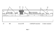
- the process of the present disclosure is illustrated for an example wherein a waveguide/grating coupler (FC), a raised grating coupler (RFC), a Ge-on-Si photodetector (PD), a Si MOSCAP modulator and a Si diode modulator are integrated on a silicon-based photonics platform.
- FC waveguide/grating coupler
- RLC raised grating coupler
- PD Ge-on-Si photodetector
- Si MOSCAP modulator Si MOSCAP modulator
- Si diode modulator Si diode modulator
- FIG. 1 shows a cross section of a planarized silicon based photonics substrate that has been processed in accordance with an existing silicon photonics platform, e.g. as reported by D. Vermeulen et al in "High-efficiency fiber-to-chip grating couplers realized using an advanced CMOS-compatible Silicon-On-Insulator platform", Optics Express, Vol. 18 No. 17, 16 August 2010, pp 18278-18283 .
- FIG. 1 shows a cross section of a planarized silicon based photonics substrate that has been processed in accordance with an existing silicon photonics platform, e.g. as reported by D. Vermeulen et al in "High-efficiency fiber-to-chip grating couplers realized using an advanced CMOS-compatible Silicon-On-Insulator platform", Optics Express, Vol. 18 No. 17, 16 August 2010, pp 18278-18283 .
- FIG. 1 shows a cross section of a planarized silicon based photonics substrate that has been
- FIG. 1 shows the 2000 nm BOX layer 1, a patterned (220 nm thick) silicon layer 2 that is doped where needed for realizing the photonics devices to be formed, with oxide regions 3 in between the silicon structures 2, a gate oxide layer 4, poly structures 5, and an oxide layer 6 having a planar surface.
- FIG. 2 illustrates etching of a trench 7 through the oxide layer 6 such that an underlying poly layer 5 is exposed, at the location where Ge growth for forming a Ge photodetector is to be initiated.
- FIG. 3 illustrates the resulting structure after etching through the poly layer 5 (stopping on the gate oxide layer 4), etching the gate oxide layer 4, and etching into the underlying crystalline silicon structure 2 to a depth e.g. in the range between 70 nm and 150 nm. In this way a template 8 for Ge growth is formed.
- a cleaning step is performed, followed by an HF dip and an in-situ H 2 bake at 850oC.
- in-situ HCI vapor etching of about 50 nm of silicon is performed in order to have a good seed layer surface.
- the photoresist (used for the patterning steps) is preferably removed after poly etching and before gate oxide etching, without exposing the silicon layer. This is advantageous for the cleanliness of the silicon seed layer surface.
- the next step in the process is the selective growth of a Ge layer 9, using the exposed silicon as a seed layer ( FIG. 4 ) and using the step-shaped trench 8 ( FIG. 3 ) as a template.
- the thickness of the Ge layer 9 can for example be in the order of 1 micrometer to 2 micrometer. For more advanced devices there may additionally be a need for silicon epitaxial growth and/or in-situ doping.
- Ge based dummy structures or Ge dummies can be provided that level out the density of Ge over the substrate. These Ge dummies can for example be formed at the location of silicon based dummy structures used in the fabrication process of the planarized silicon based photonics substrate shown in Figure 1 .
- the Ge dummies can be fabricated using the silicon based dummy structures as a seed layer for Ge growth.
- the thickness of the remaining Ge layer 10 is preferably in the order of 100 nm to 500 nm, preferably in the order of 250 nm to 300 nm.
- This step is followed by the growth of a 20 nm thick Si 0.50 Ge 0.50 cap 11 (selective with respect to the oxide 6) as illustrated in FIG. 6 , to enable in a later process step collective silicidation with the silicon devices.
- This is followed by the growth of a PECVD oxide liner 12 ( FIG. 7 ) having a thickness less than 100 nm, preferably less than 50 nm, e.g. about 30 nm.
- n+ implants 13 e.g. phosphorous
- p+ implants e.g. boron
- the Ge photodetector has an 'inverted rib' structure.
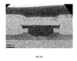
- a TEM cross section of such an 'inverted rib' structure is shown in Figure 10 .
- a planar structure comprising photonic devices and an integrated Ge photodetector on a silicon photonics platform is obtained.
- the top oxide layer 12 is thin, e.g. 30 nm thin, allowing further integration of e.g. III-V/Si hybrid lasers with good coupling to the underlying silicon photonics structures.
- FIG. 9 Integration of a III-V device is schematically illustrated in FIG. 9 , showing an integrated III-V layer 14 that allows good optical coupling to an underlying silicon waveguide structure 16. Further process steps, after bonding of the III-V layer, are mainly related to laser processing and forming contacts and interconnects.
- a single contact module can be used for forming the contacts to the silicon devices, Ge photodetectors and hybrid lasers ( FIG. 9 ).
- the shape of the Ge layer 10 is an 'inverted rib' Ge structure comprising thin laterally overhanging elements on which metal contacts 15 are provided.
- FIG. 11 illustrates a vertical p-i-n structure
- FIG. 11 (b) illustrates a lateral p-i-n structure
- FIG. 11 (c) illustrates a lateral Metal-Semiconductor-Metal structure.
- the metal contacts are provided on the thin laterally overhanging parts of the Ge structure, away from the optically active region such that optical losses at the metal contacts are strongly reduced, leading to a high responsivity of the Ge photodetector.
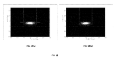
- FIG. 12 shows results of simulations performed for an 'inverted rib' Ge photodetector according to the present disclosure as described above ( FIG. 12(a) ) and for a prior art Ge waveguide-integrated photodetector with a metal contact on top of the optically active region of the Ge photodetector ( FIG. 12(b) ). Simulations were performed at a wavelength of 1.5 micrometer, assuming a Ge waveguide that is 1 micrometer wide and 0.21 micrometer thick. The simulations revealed that in the case of an 'inverted rib' Ge photodetector the absorption coefficient of the optical mode is about 4400/cm and that absorption mainly occurs in the germanium, leading to a maximum quantum efficiency approaching 100%.
- the simulation shows that the absorption coefficient of the optical mode is about 7400/cm, of which about 3000/cm is related to absorption in the metal, resulting in a maximum quantum efficiency of less than 60%.
- FIG. 13 schematically illustrates a fabrication process of the present disclosure, illustrating fabrication of an 'inverted rib' Ge waveguide-integrated photodetector according to the first aspect and fabrication of a 'laterally overgrown' Ge waveguide-integrated photodetector according to the second aspect.
- Fig. 13(a) The basis of Fig. 13(a) is a planarized silicon based photonics platform.
- the platform comprises a stack of gate oxide 4 / polycrystalline silicon 5 on a Silicon on Insulator (SOI) substrate (typical thicknesses: 160nm polycrystalline silicon 5 / 5nm gate oxide 4, on top of the SOI substrate with for instance 220 nm thick silicon 2 and 2 micron thick Buried oxide (Box) 1).
- SOI Silicon on Insulator
- Box Buried oxide
- Four or five levels of patterning have typically been performed, comprising for instance lithography and/or etching of polycrystalline silicon / silicon etching, to define advanced optical features or structures in the silicon.
- the process of fabricating the silicon based photonics platform further comprises a step of depositing an oxide and planarization of the deposited oxide, for instance by Chemical Mechanical Polishing (CMP).
- CMP Chemical Mechanical Polishing
- This CMP step can be stopped at a SiN layer on top of the patterned polycrystalline silicon.
- Preferably dummy polycrystalline silicon structures covered with SiN are provided across the substrate to level out the density of polycrystalline silicon structures accross the wafer, thus allowing good CMP process control.
- the SiN layer is removed and the oxide in between is etched back such that a planar surface if obtained.
- an oxide layer e.g. a 150 nm thick oxide layer is deposited on the entire surface.
- the resulting silicon based photonics platform is also illustrated in FIG. 1 .
- FIG. 13(a) shows a stage of the process just before the step of forming a template for Ge growth in the oxide layer.
- FIG. 13(a) illustrates providing a patterned resist layer 21 for defining the oxide template by means of for instance lithography techniques.
- FIG. 13(b) illustrates etching of trenches through the oxide layer 6 such that the underlying polycrystalline silicon layer 5 is exposed, at the location where Ge growth for forming a Ge photodetector is to be initiated.
- this is a timed oxide etch, exposing poly-silicon structures 5, wherein the etch time determines remaining oxide thickness on top of the silicon waveguide structures 2.
- FIG. 13(c) illustrates the step of etching through the polycrystalline silicon layer 5 (for instance stopping on the gate oxide 4). A step-like template in the oxide is thereby created, possibly running over underlying Si waveguide structures.
- the gate oxide layer is selectively etched ( FIG. 13(e) ), followed by in-situ cleaning and optional etching into the crystalline silicon layer to a depth e.g. in the range between 70 nm and 150 nm ( FIG.
- the next step in the process is the selective Ge growth, for instance to a thickness of 0.5 to 5 micron, using the exposed silicon as a seed layer ( FIG. 13(g) ) and using the step-shaped oxide trenches as a template.
- a post growth anneal to remove dislocation defects is performed. The removal of defects is thereby typically better for thicker layers than for thinner layers.
- Ge CMP is performed ( FIG. 13(h) ).
- the final thickness of the Ge layer is estimated to be within the range of 100 nm to 500 nm, typically about 300 nm. In the example illustrated, both an 'inverted rib' structure (left) and a 'laterally overgrown' structure (right) are obtained.
- the Ge CMP process control requires equal density of Ge islands across the wafer/design, which can be provided by providing Ge dummy structures across the wafer.
- a single, common back-end-of-line (BEOL) contacting process or strategy can be performed for Ge devices and other active Si optical devices on the same substrate.
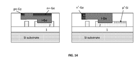
- FIG. 14 illustrates two different device configurations that may be used for the ⁇ laterally overgrown' Ge waveguide-integrated photodetector in embodiments of the present disclosure.
- the Ge active region laterally overgrown part
- the silicon waveguide structure underneath the Ge active region
- the left drawing shows a lateral p-i-n structure with both contacts to the Ge
- the right drawing shows a lateral p-i-n structure with one of the contacts (in the example shown the p+ contact) made to the silicon layer.
Landscapes
- Physics & Mathematics (AREA)
- Engineering & Computer Science (AREA)
- Microelectronics & Electronic Packaging (AREA)
- General Physics & Mathematics (AREA)
- Optics & Photonics (AREA)
- Optical Integrated Circuits (AREA)
- Light Receiving Elements (AREA)
Abstract
- providing a planarized silicon based photonics substrate comprising silicon devices including patterned silicon waveguide structures;
- depositing a dielectric layer on top of planarized silicon based photonics substrate;
- etching trenches into said dielectric layer with an appropriate etch depth, reby exposing a patterned silicon waveguide structure of said photonics substrate;
- selective etching of exposed waveguide structure, reby creating a template for Ge growth and leaving a silicon seed layer for Ge growth;
- selectively growing Ge from said seed layer, with a deliberate Ge overgrowth;
- planarizing Ge surface, leaving a Ge layer with a reduced thickness.
Description
- This disclosure relates to methods for the integration of high-performance waveguide-integrated photodetectors, e.g. Ge waveguide-integrated photodetectors, along with other photonic devices on a silicon photonics platform, e.g. a SOI based photonics platform.
- The realization of a complete silicon based photonics platform requires the co-integration of: advanced passive photonic devices, e.g. using poly-on-SOI, such as for example high-efficiency raised grating couplers, filters, polarization rotators and/or waveguides; advanced electro-optic modulators and switches, such as for example SOSCAP (semiconductor-oxide-semiconductor) modulators e.g. employing the gate-oxide capacitance between poly and SOI, and/or p-n diodes for carrier depletion and injection; hybrid III-V/Si lasers and amplifiers using bonding technology; and Ge-on Si waveguide photodetectors.
- In hybrid III-V/silicon lasers and amplifiers, optical gain is achieved in a low-defect III-V layer that is first grown epitaxially on a separate substrate and then bonded to e.g. a SOI substrate. In order to allow efficient evanescent coupling between the silicon layer and the III-V layer, both layers are in close proximity, preferably at a distance lower than 100 nm. Bonding of the III-V layer with thin interfacial layers requires a flat surface with a low topography.
- The co-integrated Ge-on-Si waveguide photodetectors preferably have a good perfomance, such as: a low dark current, requiring a low defect density of threading dislocations (less than 107 per cm2); a high responsivity in the order of 1 A/W, requiring efficient optical coupling between silicon and germanium, low parasitic absorption at the metal contacts and efficient carrier collection; and a high speed, e.g. in the range between 10 GHz and 40 GHz, requiring thin layers and a small footprint.
- Ge waveguide photodetectors can for example be integrated with a silicon photonics platform by transferring and wafer bonding a cystalline germanium film onto a silicon based (e,g, SOI) wafer, and then fabricating the photodetector in the transferred film. Using a wafer bonding approach is relatively expensive and makes co-integration with other opto-electronic components difficult, in particular the co-integration with hybrid III-V/silicon lasers, requiring bonding of III-V layers in close proximity to a silicon waveguide.
- Ge waveguide photodetectors can also be integrated with a silicon photonics platform by (e.g. epitaxially) growing a Ge layer on top of a silicon waveguide and then fabricating a Ge photodetector. In order to enable co-integration with other opto-electronic components and e.g. hybrid lasers, a planar topology is needed, requiring for example a thin germanium film for the photodetectors (preferably thinner than 300 nm). However, metal contacts on top of such a thin film are known to cause excessive optical absorption which doesn't contribute to the photocurrent, and as such negatively affects the photodetector responsivity. In addition, the negative effect on the photodetector responsivity of defects in a thin Ge layer epitaxially grown on top of silicon is much more pronounced than for a thicker Ge layer.
- It is an object of embodiments of the present disclosure to provide a method for the co-integration of photonic active and passive devices, high-performance Ge waveguide-integrated photodetectors and hybrid III-V/Si lasers on a silicon based photonics platform.
- The above objective is accomplished by a method and device according to the present disclosure.
- The present disclosure provides a method for the co-integration of advanced active and passive photonic devices, hybrid III-V/silicon lasers and Ge-on-Si waveguide detectors on a planarized silicon based photonics substrate comprising silicon devices including patterned silicon structures, e.g. waveguide structures, the method comprising: depositing a dielectric layer, e.g. a SiO2 layer, on top of the planarized silicon based photonics substrate; etching trenches into the dielectric layer with an appropriate etch depth, thereby exposing a patterned silicon waveguide structure of the photonics substrate; selective etching of the exposed waveguide structure, thereby creating a template for Ge growth and leaving a thin silicon layer as a seed layer for Ge growth; selectively growing Ge from the seed layer, with a deliberate Ge overgrowth, such as e.g. about 1 micrometer Ge overgrowth; optionally but advantageously a post-growth annealing to reduce the defect density in the Ge layer; and planarizing the Ge layer, for instance by CMP (Chemical Mechanical Polishing), thereby leaving a Ge layer with a thickness for example in the order of 100 to 500 nm, or for example in the order of 250 nm to 300 nm. The method of the present disclosure further comprises processing of the Ge photodetector, for instance comprising creating doped regions in the Ge layer, e.g. by implantation, and silicidation of both Ge and Si regions. Furthermore, III-V layers can be bonded to the substrate for the integration of hybrid III-V silicon lasers. After laser processing a common BEOL (Back-End Of Line) process can be performed to contact the lasers, Ge photodetectors and silicon devices.
- The silicon based photonics substrate or silicon based photonics platform comprises photonic structures and photonic devices, such as for example waveguide structures, grating couplers, filters and/or modulators, wherein a silicon / dielectric material system is used for realising the optical functionalities. It can for example be a Si / SiO2 material system, e.g. based on an SOI (Silicon On Insulator) wafer. This silicion based photonics substrate is preferably planarized, i.e. it has preferably a substantially planar surface.
- In embodiments of the present disclosure the template for Ge growth is selected such that it allows fabricating thin Ge photodetectors with a good performance, i.e. with a high responsivity, a low dark current, and a high speed. In a first aspect the template for Ge growth is selected such that an 'inverted rib' (T-shaped) Ge layer is obtained, for instance comprising a 100 nm to 500 nm, preferably 250 nm to 300 nm, thick optically active region with thinner (e.g. 50 nm thin) laterally overhanging parts on which metal contacts are provided. In operation, light is confined in the optically active region and is kept away from the metal contacts, thus substantially limiting absorption losses at the metal contacts. In a second aspect the template for Ge growth is selected such that a 'laterally overgrown' (L-shaped) Ge layer is obtained, wherein the optically active region (having e.g. a thickness in the order of 100nm to 500 nm, preferably 250 nm to 300 nm) in the Ge is formed by lateral overgrowth over a silicon waveguide, with a thin dielectric layer in between the silicon waveguide and the optically active region of the Ge photodetector. The optically active region of the Ge is laterally disposed, e.g. at a lateral distance (of for example 300 nm to 1000 nm) from the seed layer, and thus at a lateral distance from defects near the seed layer, e.g. resulting in a low dark current, such that the dark current is for instance below a predetermined threshold. The metal contacts to the Ge photodetector are preferably provided at a distance (of for example 50 nm or more) from the optically active region such that absorption losses at the contacts can be limited, for instance limited below a predetermined threshold.
- In a method of the present disclosure, after processing the Ge photodetectors, a planar topology is obtained. The method may further comprise bonding of III-V layers to the substrate for the integration of hybrid III-V silicon lasers. A thin dielectric layer having a thickness less than 100 nm, preferably less than 50 nm, e.g. a 30 nm thin oxide layer can be provided on this planar surface, after which for instance bonding of these III-V layers can be done, e.g. for fabricating III-V/Si hybrid lasers with good coupling to the underlying silicon structures. According to preferred embodiments of the present invention, the III-V layers are provided at a vertical distance from a silicon waveguide structure of the photonics substrate which is smaller than 100nm, or smaller than 50 nm or smaller than 30 nm.
- According to preferred embodiments, the method further comprises performing a single, common BEOL (Back-End Of Line) process to contact the III-V/silicon hybrid lasers, Ge photodetectors and silicon devices.
- According to preferred embodiments, providing the planarized silicon based photonics substrate comprises providing silicon based dummy structures on the silicon based photonics substrate and planarizing the silicon based photonics substrate by CMP. In such preferred embodiments at least a substantial amount of silicon based dummy structures can be used as a seed layer for Ge growth, thereby creating Ge based dummy structures (or Ge dummies) levelling out the density of Ge over the substrate, thus allowing good planarization of the Ge layer by means of CMP. It is an advantage that the silicon based dummy structures can be reused for creating Ge based dummy structures.
- It is an advantage of a method of the present disclosure that it fits within an existing framework, that it is CMOS compatible, and that it allows obtaining good high-performance Ge photodetectors combined with the integration of III-V/Si lasers. It is an advantage that after the integration of the Ge waveguide-integrated photodetector a planar topology is obtained, with only a thin dielectric layer (thickness less than 100 nm, preferably less than 50 nm) on top of the silicon waveguides. This allows subsequent integration of hybrid III-V/Si lasers, which rely on a thin interfacial dielectric layer between the silicon and the III-V layers to obtain optimum lasing performance.
- It is an advantage that the process of the present disclosure fits within an existing platform or framework for silicon based photonics processing, and that sharing of the contact module between all devices (lasers, Ge photodetectors, silicon devices) is enabled, potentially leading to a cost reduction.
- For purposes of summarizing the disclosure and the advantages achieved over the prior art, certain objects and advantages of the disclosure have been described herein above. Of course, it is to be understood that not necessarily all such objects or advantages may be achieved in accordance with any particular embodiment of the disclosure. Thus, for example. those skilled in the art will recognize that the disclosure may be embodied or carried out in a manner that achieves or optimizes one advantage or group of advantages as taught herein without necessarily achieving other objects or advantages as may be taught or suggested herein. Further, it is understood that this summary is merely an example and is not intended to limit the scope of the disclosure as claimed. The disclosure, both as to organization and method of operation, together with features and advantages thereof, may best be understood by reference to the following detailed description when read in conjunction with the accompanying drawings.
-
-
FIG. 1 to FIG. 8 schematically illustrate process steps of an example method according to the present disclosure. -
FIG. 9 illustrates the integration of a hybrid III-V/silicon laser according to the present disclosure. -
FIG. 10 shows a TEM cross section of an 'inverted rib' Ge structure. -
FIG. 11 illustrates different device configurations for an 'inverted rib' Ge waveguide-integrated photodetector that can be used in embodiments of the present disclosure. -
FIG. 12 shows simulation results for a prior art Ge waveguide-integrated photodetector (FIG. 12(b) ) and for an 'inverted rib' Ge waveguide-integrated photodetector according to an embodiment of the present disclosure (FIG. 12(a) ). -
FIG. 13 schematically illustrates process steps of an exemplary method according to the present disclosure. -
FIG. 14 illustrates different device configurations for a 'laterally overgrown' Ge waveguide-integrated photodetector that can be used in embodiments of the present disclosure. -
Fig. 15 andFig. 16 illustrate experimental results comparing a state of the art Ge photodetector with a Ge photodetector according to embodiments of the present invention. - Any reference signs in the claims shall not be construed as limiting the scope of the present disclosure.
- In the different drawings, the same reference signs refer to the same or analogous elements.
- In the following detailed description, numerous specific details are set forth in order to provide a thorough understanding of the disclosure and how it may be practiced in particular embodiments. However, it will be understood that the present disclosure may be practiced without these specific details. In other instances, well-known methods, procedures and techniques have not been described in detail, so as not to obscure the present disclosure. While the present disclosure will be described with respect to particular embodiments and with reference to certain drawings, the disclosure is not limited hereto. The drawings included and described herein are schematic and are not limiting the scope of the disclosure. It is also noted that in the drawings, the size of some elements may be exaggerated and, therefore, not drawn to scale for illustrative purposes.
- Furthermore, the terms first, second, third and the like in the description and in the claims, are used for distinguishing between similar elements and not necessarily for describing a sequence, either temporally, spatially, in ranking or in any other manner. It is to be understood that the terms so used are interchangeable under appropriate circumstances and that the embodiments of the disclosure described herein are capable of operation in other sequences than described or illustrated herein.
- Moreover, the terms top, bottom, over, under and the like in the description and the claims are used for descriptive purposes and not necessarily for describing relative positions. It is to be understood that the terms so used are interchangeable under appropriate circumstances and that the embodiments of the disclosure described herein are capable of operation in other orientations than described or illustrated herein.
- It is to be noticed that the term "comprising", used in the claims, should not be interpreted as being restricted to the means listed thereafter; it does not exclude other elements or steps. It is thus to be interpreted as specifying the presence of the stated features, integers, steps or components as referred to, but does not preclude the presence or addition of one or more other features, integers, steps or components, or groups thereof. Thus, the scope of the expression "a device comprising means A and B" should not be limited to devices consisting only of components A and B.
- The present disclosure provides an integration process, allowing the co-integration of photonic active and passive devices and high-performance waveguide-integrated photodetectors, e.g. high-performance Ge waveguide-integrated photodetectors and the hybrid integration of light sources, e.g. hybrid III-V/Si lasers on a single silicon based photonics platform.
- Such co-integration requires a planar technology, wherein the thickness of the Ge layers used for forming Ge photodetectors is preferably less than 300 nm.
- The method of the present disclosure comprises: depositing a dielectric layer on top of a planarized silicon based photonics substrate comprising patterned silicon structures; etching a trench into the dielectric layer with an appropriate etch depth, thereby exposing a patterned silicon waveguide structure of the photonics substrate; selectively etching the exposed waveguide structure, thereby creating a template for Ge growth and leaving a thin silicon layer as a seed layer for Ge growth; selectively growing a Ge layer using the exposed silicon of the etched waveguide as a seed layer, with a deliberate Ge overgrowth; post-growth annealing to reduce the defect density in the Ge layer; and CMP (Chemical Mechanical Polishing) of Ge to planarize the surface such that a planar structure is obtained and leaving a Ge layer with a thickness for example in the order of 250 nm to 300 nm. The method of the present disclosure further comprises processing of the Ge photodetector, comprising creating doped regions in the Ge layer, e.g. by implantation.
- In embodiments of the present disclosure the template for Ge growth is selected such that it allows fabricating thin Ge photodetectors with a good performance, i.e. with a high responsivity, a low dark current, and a high speed. In a first aspect, in order to avoid that metal contacts on such a thin Ge film cause excessive optical absorption losses, leading to a low performance of the Ge photodetectors, a design is proposed wherein the metal contacts are provided at a distance from the optically active region. This is obtained by providing an 'inverted rib' Ge photodetector, wherein the Ge is patterned such that it comprises an optically active region (e.g. 100 nm to 500 nm, preferably 250 nm to 300 nm thick) and laterally overhanging elements or parts (e.g. about 50 nm thick), resulting in a T-shape, and wherein metal contacts are provided on these overhanging elements. The laterally overhanging parts are thin, e.g. in the order of 50 nm, to confine the optical mode to the thicker, e.g. 250 nm to 300 nm thick, optically active region. The metal contacts are provided on these thin Ge layers that are laterally connected to the Ge optically active region. The light is mainly confined to the thicker Ge region and is thus kept away from the metal contacts, thereby strongly limiting absorption losses at the contacts. In a second aspect, in order to additionally minimize the influence of defects in the thin Ge layer grown on top of the silicon seed layer, a 'laterally overgrown' Ge waveguide-integrated photodetector on top of a silicon waveguide is provided. In this aspect, the optically active Ge region is formed by lateral overgrowth over a silicon waveguide, with a thin (less than 100 nm) dielectric layer in between the laterally overgrown Ge layer and the silicon waveguide layer. The optically active region of the Ge layer is at a predetermined lateral distance from the seed layer, and thus the optically active region is at a lateral distance from the defects near the seed layer. In addition, the metal contacts are preferably provided at a distance from the optically active region to minimize absorption losses at the metal contacts.
- According to the present disclosure, the 'inverted rib' Ge structure and the `laterally overgrown' Ge structure are formed by selective Ge growth seeded from a silicon layer at the bottom of an oxide trench with an appropriate etch depth and profile. As described above, the oxide trench thereby forms a template for the Ge growth and an etched silicon waveguide is used as a seed layer.
- After integration of the Ge photodetectors, a planar structure is obtained. In a later phase of the process, III-V layers can be bonded to this planar structure, e.g. for fabricating integrated III-V/silicon hybrid lasers. After laser processing a common BEOL (Back-End Of Line) approach can be used to contact the lasers, Ge photodetectors and silicon devices.
- A process of the present disclosure fits within an existing framework or platform for silicon photonics processing. It is CMOS compatible, and it allows obtaining good Ge photodetectors combined with the integration of III-V/Si lasers. After the integration of the Ge waveguide-integrated photodetectors a planar topology is obtained, with only a thin dielectric layer (thickness less than 100 nm, preferably less than 50 nm) on top of the silicon waveguides. This allows subsequent integration of hybrid III-V/Si lasers, which rely on a thin interfacial dielectric layer between the silicon and the III-V layers to obtain optimum lasing performance. In a process of the present disclosure sharing of the contact module between all devices (lasers, Ge photodetectors, silicon devices) is enabled, potentially leading to a low cost process.
- The method of the present disclosure is further described for an exemplary process flow, with a focus on the process steps for forming the Ge photodetectors. However, the present disclosure is not limited thereto. For example, in the different process steps other suitable materials, other suitable process parameters (such as temperatures, process times, ...) and other suitable dimensions can be used. Other devices than the ones illustrated can be integrated.
- Process steps of an exemplary process flow according to an embodiment of the present disclosure are schematically illustrated in
FIG. 1 to FIG. 8 . In these drawings, the process of the present disclosure is illustrated for an example wherein a waveguide/grating coupler (FC), a raised grating coupler (RFC), a Ge-on-Si photodetector (PD), a Si MOSCAP modulator and a Si diode modulator are integrated on a silicon-based photonics platform. - In the example shown, a photonics SOI wafer is used, the SOI wafer comprising a 2000 nm thick BOX (Buried Oxide) layer with a lightly p-doped, 220 nm thick silicon layer on top.
FIG. 1 shows a cross section of a planarized silicon based photonics substrate that has been processed in accordance with an existing silicon photonics platform, e.g. as reported by D. Vermeulen et al in "High-efficiency fiber-to-chip grating couplers realized using an advanced CMOS-compatible Silicon-On-Insulator platform", Optics Express, Vol. 18 No. 17, 16 August 2010, pp 18278-18283.FIG. 1 shows the 2000nm BOX layer 1, a patterned (220 nm thick)silicon layer 2 that is doped where needed for realizing the photonics devices to be formed, withoxide regions 3 in between thesilicon structures 2, agate oxide layer 4,poly structures 5, and anoxide layer 6 having a planar surface. - In the following steps, a template for Ge growth is formed.
FIG. 2 illustrates etching of atrench 7 through theoxide layer 6 such that anunderlying poly layer 5 is exposed, at the location where Ge growth for forming a Ge photodetector is to be initiated.FIG. 3 illustrates the resulting structure after etching through the poly layer 5 (stopping on the gate oxide layer 4), etching thegate oxide layer 4, and etching into the underlyingcrystalline silicon structure 2 to a depth e.g. in the range between 70 nm and 150 nm. In this way atemplate 8 for Ge growth is formed. Next a cleaning step is performed, followed by an HF dip and an in-situ H2 bake at 850ºC. Then in-situ HCI vapor etching of about 50 nm of silicon is performed in order to have a good seed layer surface. In this process, the photoresist (used for the patterning steps) is preferably removed after poly etching and before gate oxide etching, without exposing the silicon layer. This is advantageous for the cleanliness of the silicon seed layer surface. - The next step in the process is the selective growth of a Ge layer 9, using the exposed silicon as a seed layer (
FIG. 4 ) and using the step-shaped trench 8 (FIG. 3 ) as a template. The thickness of the Ge layer 9 can for example be in the order of 1 micrometer to 2 micrometer. For more advanced devices there may additionally be a need for silicon epitaxial growth and/or in-situ doping. - After a Ge post-growth anneal (e.g. 3 minutes at 850°C in a nitrogen atmosphere) to reduce the number of defects, a Ge CMP step, stopping on the
silicon oxide layer 6 is performed (FIG. 5 ). In order to be able to better control the Ge CMP process, Ge based dummy structures or Ge dummies can be provided that level out the density of Ge over the substrate. These Ge dummies can for example be formed at the location of silicon based dummy structures used in the fabrication process of the planarized silicon based photonics substrate shown inFigure 1 . For example, the Ge dummies can be fabricated using the silicon based dummy structures as a seed layer for Ge growth. After Ge CMP, the thickness of the remainingGe layer 10 is preferably in the order of 100 nm to 500 nm, preferably in the order of 250 nm to 300 nm. - This step is followed by the growth of a 20 nm thick Si0.50Ge0.50 cap 11 (selective with respect to the oxide 6) as illustrated in
FIG. 6 , to enable in a later process step collective silicidation with the silicon devices. This is followed by the growth of a PECVD oxide liner 12 (FIG. 7 ) having a thickness less than 100 nm, preferably less than 50 nm, e.g. about 30 nm. Next, n+ implants 13 (e.g. phosphorous) and/or p+ implants (e.g. boron) in the Ge layer are performed, followed by an activation anneal, for forming a photodetector structure (vertical p-i-n in the example shown inFIG. 8 ). In the example shown inFIG. 8 , the Ge photodetector has an 'inverted rib' structure. A TEM cross section of such an 'inverted rib' structure is shown inFigure 10 . - At this stage of the process, a planar structure comprising photonic devices and an integrated Ge photodetector on a silicon photonics platform is obtained. The
top oxide layer 12 is thin, e.g. 30 nm thin, allowing further integration of e.g. III-V/Si hybrid lasers with good coupling to the underlying silicon photonics structures. - Integration of a III-V device is schematically illustrated in
FIG. 9 , showing an integrated III-V layer 14 that allows good optical coupling to an underlyingsilicon waveguide structure 16. Further process steps, after bonding of the III-V layer, are mainly related to laser processing and forming contacts and interconnects. In a process of the present disclosure, a single contact module can be used for forming the contacts to the silicon devices, Ge photodetectors and hybrid lasers (FIG. 9 ). - As can be seen in
FIG. 9 , in the example shown the shape of theGe layer 10 is an 'inverted rib' Ge structure comprising thin laterally overhanging elements on whichmetal contacts 15 are provided. This is also illustrated inFIG. 11 for different electrical design variants of the Ge photodetector.FIG. 11 (a) illustrates a vertical p-i-n structure;FIG 11 (b) illustrates a lateral p-i-n structure andFIG. 11 (c) illustrates a lateral Metal-Semiconductor-Metal structure. The metal contacts are provided on the thin laterally overhanging parts of the Ge structure, away from the optically active region such that optical losses at the metal contacts are strongly reduced, leading to a high responsivity of the Ge photodetector. -
FIG. 12 shows results of simulations performed for an 'inverted rib' Ge photodetector according to the present disclosure as described above (FIG. 12(a) ) and for a prior art Ge waveguide-integrated photodetector with a metal contact on top of the optically active region of the Ge photodetector (FIG. 12(b) ). Simulations were performed at a wavelength of 1.5 micrometer, assuming a Ge waveguide that is 1 micrometer wide and 0.21 micrometer thick. The simulations revealed that in the case of an 'inverted rib' Ge photodetector the absorption coefficient of the optical mode is about 4400/cm and that absorption mainly occurs in the germanium, leading to a maximum quantum efficiency approaching 100%. In case of a prior art Ge photodetector, the simulation shows that the absorption coefficient of the optical mode is about 7400/cm, of which about 3000/cm is related to absorption in the metal, resulting in a maximum quantum efficiency of less than 60%. -
FIG. 13 schematically illustrates a fabrication process of the present disclosure, illustrating fabrication of an 'inverted rib' Ge waveguide-integrated photodetector according to the first aspect and fabrication of a 'laterally overgrown' Ge waveguide-integrated photodetector according to the second aspect. - The basis of
Fig. 13(a) is a planarized silicon based photonics platform. The platform comprises a stack ofgate oxide 4 /polycrystalline silicon 5 on a Silicon on Insulator (SOI) substrate (typical thicknesses: 160nmpolycrystalline silicon 5 /5nm gate oxide 4, on top of the SOI substrate with for instance 220 nmthick silicon FIG. 1 . -
FIG. 13(a) shows a stage of the process just before the step of forming a template for Ge growth in the oxide layer.FIG. 13(a) illustrates providing a patterned resistlayer 21 for defining the oxide template by means of for instance lithography techniques.FIG. 13(b) illustrates etching of trenches through theoxide layer 6 such that the underlyingpolycrystalline silicon layer 5 is exposed, at the location where Ge growth for forming a Ge photodetector is to be initiated. Preferably, this is a timed oxide etch, exposing poly-silicon structures 5, wherein the etch time determines remaining oxide thickness on top of thesilicon waveguide structures 2. In the example shown, the trench at the left is shaped to realize an 'inverted rib' Ge structure; the trench at the right is shaped such that it overlies a silicon waveguide, intended for realizing a 'laterally overgrown' Ge structure.FIG. 13(c) illustrates the step of etching through the polycrystalline silicon layer 5 (for instance stopping on the gate oxide 4). A step-like template in the oxide is thereby created, possibly running over underlying Si waveguide structures. After stripping the resist layer (FIG. 13(d) ) the gate oxide layer is selectively etched (FIG. 13(e) ), followed by in-situ cleaning and optional etching into the crystalline silicon layer to a depth e.g. in the range between 70 nm and 150 nm (FIG. 13(f) ). The next step in the process is the selective Ge growth, for instance to a thickness of 0.5 to 5 micron, using the exposed silicon as a seed layer (FIG. 13(g) ) and using the step-shaped oxide trenches as a template. Advantageously, a post growth anneal to remove dislocation defects is performed. The removal of defects is thereby typically better for thicker layers than for thinner layers. Afterwards,Ge CMP is performed (FIG. 13(h) ). The final thickness of the Ge layer is estimated to be within the range of 100 nm to 500 nm, typically about 300 nm. In the example illustrated, both an 'inverted rib' structure (left) and a 'laterally overgrown' structure (right) are obtained. The Ge CMP process control requires equal density of Ge islands across the wafer/design, which can be provided by providing Ge dummy structures across the wafer. A single, common back-end-of-line (BEOL) contacting process or strategy can be performed for Ge devices and other active Si optical devices on the same substrate. - As an example,
FIG. 14 illustrates two different device configurations that may be used for the `laterally overgrown' Ge waveguide-integrated photodetector in embodiments of the present disclosure. Note that in between (in vertical direction) the Ge active region (laterally overgrown part) and the silicon waveguide structure (underneath the Ge active region) there is a thin oxide layer. The left drawing shows a lateral p-i-n structure with both contacts to the Ge, while the right drawing shows a lateral p-i-n structure with one of the contacts (in the example shown the p+ contact) made to the silicon layer. - Experimental results with respect to the measured responsivity as a function of device width, both for 'regular' (
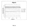
Fig. 15 ) and 'inverted rib' (Fig. 16 ) Ge photodetector structures, for a wavelength of 1.5 micrometer, are provided. The final thickness of the Ge layer was about 200 nm. Results are shown for devices with 10 micrometer length (L10) and for different widths (W=1.4 micron, 2 micron, 3 micron and 1 micron, 2 micron respectively). It can be concluded that for the same device size, a clearly better responsivity is obtained for the inverted rib structure according to aspects of the present invention as compared to a "regular" Ge photodetector. It can also be concluded that the responsivity is much less influenced by device width in the case of an inverted rib structure as compared to a regular structure. - Other variations to the disclosed embodiments can be understood and effected by those skilled in the art in practicing the claimed invention, from a study of the drawings, the disclosure and the appended claims. In the claims, the word "comprising" does not exclude other elements or steps, and the indefinite article "a" or "an" does not exclude a plurality. The mere fact that certain measures are recited in mutually different dependent claims does not indicate that a combination of these measures cannot be used to advantage. Any reference signs in the claims should not be construed as limiting the scope.
- The foregoing description details certain embodiments of the invention. It will be appreciated, however, that no matter how detailed the foregoing appears in text, the invention may be practiced in many ways. It should be noted that the use of particular terminology when describing certain features or aspects of the invention should not be taken to imply that the terminology is being re-defined herein to be restricted to include any specific characteristics of the features or aspects of the invention with which that terminology is associated.
Claims (14)
- A method for the co-integration of photonic devices, Ge waveguide-integrated photodetectors and hybrid III-V/Si lasers on a silicon based photonics platform, the method comprising:- providing a planarized silicon based photonics substrate comprising silicon devices including patterned silicon waveguide structures;- depositing a dielectric layer on top of the planarized silicon based photonics substrate;- etching trenches into said dielectric layer with an appropriate etch depth, thereby exposing a patterned silicon waveguide structure of said photonics substrate;- selective etching of the exposed waveguide structure, thereby creating a template for Ge growth and leaving a silicon seed layer for Ge growth;- selectively growing Ge from said seed layer, with a deliberate Ge overgrowth;- planarizing the Ge surface, leaving a Ge layer with a reduced thickness.
- Method according to claim 1, further comprising a post-growth annealing to reduce the defect density in the Ge layer, before planarizing said Ge surface.
- Method according to claim 1 or 2, wherein said Ge layer with a reduced thickness has a thickness between 100 and 500 nm.
- Method according to claim 1 to 3, wherein planarizing said Ge surface comprises a CMP process.
- Method according to any of the previous claims, further comprises processing of a Ge photodetector.
- Method according to any of the previous claims, further comprising providing metal contacts to the Ge photodetector at a distance from the optically active region such that absorption losses at the contacts are limited below a predetermined threshold.
- Method according to any of the previous claims, further comprising selecting the template for Ge growth such that an inverted rib, for instance T-shaped, Ge layer is obtained.
- A method according to claim 7, wherein said inverted rib comprises a 250 nm to 300 nm thick optically active region with thinner laterally overhanging parts on which metal contacts can be provided.
- A method according to any of the previous claims, wherein the template for Ge growth is selected such that a laterally overgrown, for instance L-shaped Ge layer is obtained, wherein the optically active region in the Ge is formed by lateral overgrowth over a silicon waveguide.
- Method according to claim 9, wherein the template for Ge growth is selected such that the optically active region of the Ge is laterally disposed from, e.g. is at a lateral distance of, the seed layer, and thus at a sufficiently large lateral distance from defects near the seed layer, in order to reduce a dark current below a predetermined threshold.
- Method according to any of the previous claims, further comprising bonding III-V layers to the substrate for the integration of hybrid III-V silicon lasers.
- Method according to claim 11, wherein said III-V layers are provided at a vertical distance from a silicon waveguide structure of said photonics substrate which is smaller than 100 nm.
- Method according to any of claims 11 or 12, further comprising performing a single, common Back-End-Of-Line process to contact the hybrid III-V silicon lasers, Ge photodetectors and silicon devices.
- Method according to any of the previous claims, wherein providing said planarized silicon based photonics substrate comprises providing dummy structures on said silicon based photonics substrate and planarizing said silicon based photonics substrate by CMP, and wherein said dummy structures are used as a seed layer for Ge growth, thereby creating Ge based dummy structures allowing good planarization of the Ge layer by means of CMP.
Applications Claiming Priority (1)
| Application Number | Priority Date | Filing Date | Title |
|---|---|---|---|
| US201161484064P | 2011-05-09 | 2011-05-09 |
Publications (2)
| Publication Number | Publication Date |
|---|---|
| EP2523026A1 true EP2523026A1 (en) | 2012-11-14 |
| EP2523026B1 EP2523026B1 (en) | 2016-04-27 |
Family
ID=46395454
Family Applications (1)
| Application Number | Title | Priority Date | Filing Date |
|---|---|---|---|
| EP12167332.1A Active EP2523026B1 (en) | 2011-05-09 | 2012-05-09 | Co-integration of photonic devices on a silicon photonics platform |
Country Status (3)
| Country | Link |
|---|---|
| US (1) | US8741684B2 (en) |
| EP (1) | EP2523026B1 (en) |
| JP (1) | JP5969811B2 (en) |
Cited By (8)
| Publication number | Priority date | Publication date | Assignee | Title |
|---|---|---|---|---|
| US9407066B2 (en) | 2013-07-24 | 2016-08-02 | GlobalFoundries, Inc. | III-V lasers with integrated silicon photonic circuits |
| US9461090B2 (en) | 2014-07-03 | 2016-10-04 | Globalfoundries Inc. | Photodetector and method of forming the photodetector on stacked trench isolation regions |
| US9864138B2 (en) | 2015-01-05 | 2018-01-09 | The Research Foundation For The State University Of New York | Integrated photonics including germanium |
| EP3349252A4 (en) * | 2016-02-29 | 2018-12-26 | Huawei Technologies Co., Ltd. | Optical waveguide detector and optical module |
| FR3078826A1 (en) * | 2018-03-07 | 2019-09-13 | Stmicroelectronics (Crolles 2) Sas | VERTICAL PHOTODIODE |
| CN113253490A (en) * | 2020-02-11 | 2021-08-13 | 台湾积体电路制造股份有限公司 | Semiconductor device and method of forming the same |
| EP4033279A1 (en) * | 2013-03-07 | 2022-07-27 | Aurrion, Inc. | Simultaneous processing of multiple photonic device layers |
| EP4456149A1 (en) * | 2023-04-28 | 2024-10-30 | Cisco Technology, Inc. | Waveguide integrated photodiode |
Families Citing this family (50)
| Publication number | Priority date | Publication date | Assignee | Title |
|---|---|---|---|---|
| US9368579B2 (en) | 2012-02-07 | 2016-06-14 | The Board Of Trustees Of The Leland Stanford Junior University | Selective area growth of germanium and silicon-germanium in silicon waveguides for on-chip optical interconnect applications |
| US20140270629A1 (en) * | 2013-03-15 | 2014-09-18 | Apic Corporation | Optical waveguide network of an interconnecting ic module |
| JP6020295B2 (en) * | 2013-03-28 | 2016-11-02 | 富士通株式会社 | Si optical integrated circuit device and manufacturing method thereof |
| US9048371B2 (en) * | 2013-10-03 | 2015-06-02 | Globalfoundries Singapore Pte. Ltd. | Semiconductor devices including avalanche photodetector diodes integrated on waveguides and methods for fabricating the same |
| JP2015111260A (en) | 2013-11-11 | 2015-06-18 | 住友電気工業株式会社 | Optical semiconductor device manufacturing method and optical semiconductor device |
| US9231131B2 (en) | 2014-01-07 | 2016-01-05 | International Business Machines Corporation | Integrated photodetector waveguide structure with alignment tolerance |
| US9766484B2 (en) | 2014-01-24 | 2017-09-19 | Cisco Technology, Inc. | Electro-optical modulator using waveguides with overlapping ridges |
| US9627575B2 (en) * | 2014-09-11 | 2017-04-18 | International Business Machines Corporation | Photodiode structures |
| US9372307B1 (en) * | 2015-03-30 | 2016-06-21 | International Business Machines Corporation | Monolithically integrated III-V optoelectronics with SI CMOS |
| US10288804B2 (en) | 2015-07-06 | 2019-05-14 | University Of Houston System | Method to fabricate chip-scale electronic photonic (plasmonic)-integrated circuits |
| JP2017022175A (en) * | 2015-07-07 | 2017-01-26 | ルネサスエレクトロニクス株式会社 | Semiconductor device and manufacturing method thereof |
| JP6641765B2 (en) | 2015-08-05 | 2020-02-05 | 富士通オプティカルコンポーネンツ株式会社 | Optical communication device and optical module |
| JP6533131B2 (en) * | 2015-09-04 | 2019-06-19 | ルネサスエレクトロニクス株式会社 | Semiconductor device manufacturing method |
| JP6545608B2 (en) * | 2015-11-30 | 2019-07-17 | ルネサスエレクトロニクス株式会社 | Semiconductor device and method of manufacturing the same |
| JP2017146364A (en) * | 2016-02-15 | 2017-08-24 | 富士通株式会社 | Optical semiconductor device and optical semiconductor module |
| US9711662B1 (en) * | 2016-04-21 | 2017-07-18 | Globalfoundries Singapore Pte. Ltd. | Integrated circuits with optical modulators and photodetectors and methods for producing the same |
| CN109642985B (en) * | 2016-07-13 | 2021-03-12 | 洛克利光子有限公司 | Mode converter and method of making the same |
| US10976491B2 (en) | 2016-11-23 | 2021-04-13 | The Research Foundation For The State University Of New York | Photonics interposer optoelectronics |
| US9927572B1 (en) | 2017-01-04 | 2018-03-27 | Hewlett Packard Enterprise Development Lp | Hybrid photonic device structures |
| US10698156B2 (en) | 2017-04-27 | 2020-06-30 | The Research Foundation For The State University Of New York | Wafer scale bonded active photonics interposer |
| FR3067866B1 (en) * | 2017-06-19 | 2022-01-14 | Commissariat Energie Atomique | HYBRID SEMICONDUCTOR LASER COMPONENT AND METHOD FOR MAKING SUCH A COMPONENT |
| CN108461629A (en) * | 2018-03-02 | 2018-08-28 | 福建省福芯电子科技有限公司 | Silicon substrate radio frequency capacitance and preparation method thereof |
| KR20220124298A (en) | 2018-04-04 | 2022-09-14 | 더 리서치 파운데이션 포 더 스테이트 유니버시티 오브 뉴욕 | Heterogeneous structures on integrated photonics platforms |
| US10816724B2 (en) | 2018-04-05 | 2020-10-27 | The Research Foundation For The State University Of New York | Fabricating photonics structure light signal transmission regions |
| FR3082354B1 (en) * | 2018-06-08 | 2020-07-17 | Commissariat A L'energie Atomique Et Aux Energies Alternatives | PHOTONIC CHIP CROSSED BY A VIA |
| US10690853B2 (en) | 2018-06-25 | 2020-06-23 | International Business Machines Corporation | Optoelectronics integration using semiconductor on insulator substrate |
| KR102601212B1 (en) | 2018-10-10 | 2023-11-10 | 삼성전자주식회사 | integrated circuit device including photoelectronic element |
| US11029466B2 (en) | 2018-11-21 | 2021-06-08 | The Research Foundation For The State University Of New York | Photonics structure with integrated laser |
| US11550099B2 (en) * | 2018-11-21 | 2023-01-10 | The Research Foundation For The State University Of New York | Photonics optoelectrical system |
| TWI851601B (en) | 2018-11-21 | 2024-08-11 | 紐約州立大學研究基金會 | Photonics optoelectrical system and method for fabricating same |
| CN114365039B (en) | 2019-06-10 | 2025-05-09 | 迈络思科技有限公司 | Photoelectric device and method for manufacturing the same |
| KR20220086548A (en) | 2019-06-18 | 2022-06-23 | 더 리서치 파운데이션 포 더 스테이트 유니버시티 오브 뉴욕 | Photonic Structure Conductive Light Path Fabrication |
| WO2021077104A1 (en) * | 2019-10-18 | 2021-04-22 | PsiQuantum Corp. | Electro-optical device fabricated on a substrate and comprising ferroelectric layer epitaxially grown on the substrate |
| US11810986B2 (en) * | 2019-11-15 | 2023-11-07 | Institute of Microelectronics, Chinese Academy of Sciences | Method for integrating surface-electrode ion trap and silicon photoelectronic device, integrated structure, and three-dimensional structure |
| US11233159B2 (en) | 2020-01-10 | 2022-01-25 | Newport Fab, Llc | Fabrication of semiconductor structure having group III-V device on group IV substrate with separately formed contacts using different metal liners |
| US11545587B2 (en) | 2020-01-10 | 2023-01-03 | Newport Fab, Llc | Semiconductor structure having group III-V device on group IV substrate and contacts with liner stacks |
| US11349280B2 (en) | 2020-01-10 | 2022-05-31 | Newport Fab, Llc | Semiconductor structure having group III-V device on group IV substrate |
| US11581452B2 (en) * | 2020-01-10 | 2023-02-14 | Newport Fab, Llc | Semiconductor structure having group III-V device on group IV substrate and contacts with precursor stacks |
| US11296482B2 (en) | 2020-01-10 | 2022-04-05 | Newport Fab, Llc | Semiconductor structure having group III-V chiplet on group IV substrate and cavity in proximity to heating element |
| US11929442B2 (en) | 2020-01-10 | 2024-03-12 | Newport Fab, Llc | Structure and method for process control monitoring for group III-V devices integrated with group IV substrate |
| US11764543B2 (en) | 2020-04-23 | 2023-09-19 | Mellanox Technologies, Ltd. | Integration of modulator and laser in a single chip |
| WO2021227912A1 (en) * | 2020-05-14 | 2021-11-18 | 上海新微技术研发中心有限公司 | Silicon-based optoelectronic device based on silicon photonics interposer technology, and preparation method therefor |
| CN112186075B (en) * | 2020-10-10 | 2023-05-23 | 中国科学院微电子研究所 | Waveguide type photoelectric detector and manufacturing method thereof |
| US12442979B2 (en) * | 2021-09-22 | 2025-10-14 | Intel Corporation | Optical waveguide formed within in a glass layer |
| US12298560B2 (en) * | 2021-11-10 | 2025-05-13 | Intel Corporation | Germanium waveguide photodetector with integrated heater |
| CN114400236B (en) * | 2022-01-16 | 2024-04-26 | Nano科技(北京)有限公司 | Silicon photonic integrated chip integrating silicon photonic modulator and silicon germanium detector and preparation method thereof |
| CN115632074A (en) * | 2022-10-20 | 2023-01-20 | 杭州光智元科技有限公司 | Photodetector and method for manufacturing same |
| US12560763B2 (en) | 2023-09-28 | 2026-02-24 | International Business Machines Corporation | Embedded SiGe optical waveguide with low defectivity |
| US12607887B2 (en) * | 2023-10-23 | 2026-04-21 | Hewlett Packard Enterprise Development Lp | Heterogeneous III-V/Si (de-) interleaver filters with non-volatile memristive functionality |
| CN119008758B (en) * | 2024-08-13 | 2025-12-12 | 中国科学院半导体研究所 | A waveguide-coupled photodetector and its fabrication method |
Citations (3)
| Publication number | Priority date | Publication date | Assignee | Title |
|---|---|---|---|---|
| US6075253A (en) * | 1997-04-15 | 2000-06-13 | Nec Corporation | Monocrystalline semiconductor photodetector |
| US20080153267A1 (en) * | 2006-12-21 | 2008-06-26 | Commissariat A L'energie Atomique | Method for manufacturing a soi substrate associating silicon based areas and gaas based areas |
| US20090108384A1 (en) * | 2007-10-26 | 2009-04-30 | Solomon Assefa | Optoelectronic Device with Germanium Photodetector |
Family Cites Families (12)
| Publication number | Priority date | Publication date | Assignee | Title |
|---|---|---|---|---|
| ATE202630T1 (en) * | 1996-08-16 | 2001-07-15 | Zeptosens Ag | OPTICAL DETECTION DEVICE |
| US7453132B1 (en) | 2002-06-19 | 2008-11-18 | Luxtera Inc. | Waveguide photodetector with integrated electronics |
| US7012314B2 (en) * | 2002-12-18 | 2006-03-14 | Agere Systems Inc. | Semiconductor devices with reduced active region defects and unique contacting schemes |
| US6897498B2 (en) | 2003-03-31 | 2005-05-24 | Sioptical, Inc. | Polycrystalline germanium-based waveguide detector integrated on a thin silicon-on-insulator (SOI) platform |
| US7209623B2 (en) | 2005-05-03 | 2007-04-24 | Intel Corporation | Semiconductor waveguide-based avalanche photodetector with separate absorption and multiplication regions |
| JP4621081B2 (en) * | 2005-07-07 | 2011-01-26 | Okiセミコンダクタ株式会社 | Manufacturing method of semiconductor device |
| FR2896337A1 (en) * | 2006-01-17 | 2007-07-20 | St Microelectronics Crolles 2 | METHOD FOR MAKING A MONOCRYSTALLINE LAYER ON A DIELECTRIC LAYER |
| US7613369B2 (en) | 2006-04-13 | 2009-11-03 | Luxtera, Inc. | Design of CMOS integrated germanium photodiodes |
| JP5232981B2 (en) | 2008-03-07 | 2013-07-10 | 日本電気株式会社 | SiGe photodiode |
| US7972922B2 (en) * | 2008-11-21 | 2011-07-05 | Freescale Semiconductor, Inc. | Method of forming a semiconductor layer |
| JP5204059B2 (en) * | 2009-09-04 | 2013-06-05 | 日本電信電話株式会社 | Photodetector manufacturing method |
| WO2011104317A1 (en) * | 2010-02-24 | 2011-09-01 | Universiteit Gent | Laser light coupling into soi cmos photonic integrated circuit |
-
2012
- 2012-05-08 JP JP2012106604A patent/JP5969811B2/en active Active
- 2012-05-08 US US13/466,766 patent/US8741684B2/en active Active
- 2012-05-09 EP EP12167332.1A patent/EP2523026B1/en active Active
Patent Citations (3)
| Publication number | Priority date | Publication date | Assignee | Title |
|---|---|---|---|---|
| US6075253A (en) * | 1997-04-15 | 2000-06-13 | Nec Corporation | Monocrystalline semiconductor photodetector |
| US20080153267A1 (en) * | 2006-12-21 | 2008-06-26 | Commissariat A L'energie Atomique | Method for manufacturing a soi substrate associating silicon based areas and gaas based areas |
| US20090108384A1 (en) * | 2007-10-26 | 2009-04-30 | Solomon Assefa | Optoelectronic Device with Germanium Photodetector |
Non-Patent Citations (1)
| Title |
|---|
| D. VERMEULEN ET AL.: "High-efficiency fiber-to-chip grating couplers realized using an advanced CMOS-compatible Silicon-On-Insulator platform", OPTICS EXPRESS, vol. 18, no. 17, 16 August 2010 (2010-08-16), pages 18278 - 18283, XP055263777 |
Cited By (20)
| Publication number | Priority date | Publication date | Assignee | Title |
|---|---|---|---|---|
| EP4033279A1 (en) * | 2013-03-07 | 2022-07-27 | Aurrion, Inc. | Simultaneous processing of multiple photonic device layers |
| US9966735B2 (en) | 2013-07-24 | 2018-05-08 | Globalfoundries Inc. | III-V lasers with integrated silicon photonic circuits |
| US9407066B2 (en) | 2013-07-24 | 2016-08-02 | GlobalFoundries, Inc. | III-V lasers with integrated silicon photonic circuits |
| US10163955B2 (en) | 2014-07-03 | 2018-12-25 | Globalfoundries Inc. | Photodetector and method of forming the photodetector on stacked trench isolation regions |
| US9461090B2 (en) | 2014-07-03 | 2016-10-04 | Globalfoundries Inc. | Photodetector and method of forming the photodetector on stacked trench isolation regions |
| US9799693B2 (en) | 2014-07-03 | 2017-10-24 | Globalfoundries Inc. | Photodetector and method of forming the photodetector on stacked trench isolation regions |
| US10295745B2 (en) | 2015-01-05 | 2019-05-21 | The Research Foundation For The State University Of New York | Integrated photonics including germanium |
| US9864138B2 (en) | 2015-01-05 | 2018-01-09 | The Research Foundation For The State University Of New York | Integrated photonics including germanium |
| US11703643B2 (en) | 2015-01-05 | 2023-07-18 | The Research Foundation For The State University Of New York | Integrated photonics including waveguiding material |
| US10571631B2 (en) | 2015-01-05 | 2020-02-25 | The Research Foundation For The State University Of New York | Integrated photonics including waveguiding material |
| US10830952B2 (en) | 2015-01-05 | 2020-11-10 | The Research Foundation For The State University Of New York | Integrated photonics including germanium |
| EP3349252A4 (en) * | 2016-02-29 | 2018-12-26 | Huawei Technologies Co., Ltd. | Optical waveguide detector and optical module |
| US10446707B2 (en) | 2016-02-29 | 2019-10-15 | Huawei Technologies Co., Ltd. | Optical waveguide detector and optical module |
| FR3078826A1 (en) * | 2018-03-07 | 2019-09-13 | Stmicroelectronics (Crolles 2) Sas | VERTICAL PHOTODIODE |
| US11107941B2 (en) | 2018-03-07 | 2021-08-31 | Stmicroelectronics (Crolles 2) Sas | Vertical photodiode |
| CN116014013A (en) * | 2018-03-07 | 2023-04-25 | 意法半导体(克洛尔2)公司 | vertical photodiode |
| CN110246915A (en) * | 2018-03-07 | 2019-09-17 | 意法半导体(克洛尔2)公司 | Vertical photodiode |
| US11784275B2 (en) | 2018-03-07 | 2023-10-10 | Stmicroelectronics (Crolles 2) Sas | Vertical photodiode |
| CN113253490A (en) * | 2020-02-11 | 2021-08-13 | 台湾积体电路制造股份有限公司 | Semiconductor device and method of forming the same |
| EP4456149A1 (en) * | 2023-04-28 | 2024-10-30 | Cisco Technology, Inc. | Waveguide integrated photodiode |
Also Published As
| Publication number | Publication date |
|---|---|
| US20120288971A1 (en) | 2012-11-15 |
| JP2012256869A (en) | 2012-12-27 |
| JP5969811B2 (en) | 2016-08-17 |
| EP2523026B1 (en) | 2016-04-27 |
| US8741684B2 (en) | 2014-06-03 |
Similar Documents
| Publication | Publication Date | Title |
|---|---|---|
| EP2523026B1 (en) | Co-integration of photonic devices on a silicon photonics platform | |
| US11029466B2 (en) | Photonics structure with integrated laser | |
| US10838240B2 (en) | Electro-absorption modulator | |
| US9413139B2 (en) | Hybrid waveguide lasers and methods for fabricating hybrid waveguide lasers | |
| US7217584B2 (en) | Bonded thin-film structures for optical modulators and methods of manufacture | |
| KR101952800B1 (en) | Vertical pn silicon modulator | |
| US8723125B1 (en) | Waveguide end-coupled infrared detector | |
| EP3471221B1 (en) | Active-passive waveguide photonic system | |
| US11075498B2 (en) | Method of fabricating an optoelectronic component | |
| JP2007300095A (en) | Method for manufacturing vertical sidewalls on a (110) silicon substrate for Si / SiGe photodetectors | |
| JP2013505485A (en) | Optical modulator using wafer bonding technology | |
| US8415185B2 (en) | Process for making a slot-type optical waveguide on silicon | |
| US10690852B2 (en) | III-V semiconductor waveguide nanoridge structure | |
| CN112204459B (en) | Electroabsorption modulator | |
| CN105556680A (en) | Microstructure-enhanced absorption photosensitive device | |
| JP2020500332A (en) | Photoelectric device | |
| US20200057198A1 (en) | Grating with plurality of layers | |
| US11256113B2 (en) | Optical structure and method of fabricating an optical structure | |
| US20050207704A1 (en) | Low loss contact structures for silicon based optical modulators and methods of manufacture | |
| CN109478764B (en) | Integrated photonic devices, methods and applications based on heterostructures | |
| GB2580264A (en) | Optical modulator and method of fabricating an optical modulator | |
| CN111816733B (en) | Pretreatment method for selective germanium epitaxy in waveguide germanium detector manufacturing process | |
| US7865053B2 (en) | Multi-semiconductor slab electro-optic modulator and process for using the same | |
| CN111987585A (en) | Silicon waveguide output laser | |
| US20190019902A1 (en) | Silicon waveguide integrated with germanium pin photodetector |
Legal Events
| Date | Code | Title | Description |
|---|---|---|---|
| PUAI | Public reference made under article 153(3) epc to a published international application that has entered the european phase |
Free format text: ORIGINAL CODE: 0009012 |
|
| AK | Designated contracting states |
Kind code of ref document: A1 Designated state(s): AL AT BE BG CH CY CZ DE DK EE ES FI FR GB GR HR HU IE IS IT LI LT LU LV MC MK MT NL NO PL PT RO RS SE SI SK SM TR |
|
| AX | Request for extension of the european patent |
Extension state: BA ME |
|
| 17P | Request for examination filed |
Effective date: 20130510 |
|
| GRAP | Despatch of communication of intention to grant a patent |
Free format text: ORIGINAL CODE: EPIDOSNIGR1 |
|
| INTG | Intention to grant announced |
Effective date: 20160126 |
|
| GRAS | Grant fee paid |
Free format text: ORIGINAL CODE: EPIDOSNIGR3 |
|
| GRAA | (expected) grant |
Free format text: ORIGINAL CODE: 0009210 |
|
| AK | Designated contracting states |
Kind code of ref document: B1 Designated state(s): AL AT BE BG CH CY CZ DE DK EE ES FI FR GB GR HR HU IE IS IT LI LT LU LV MC MK MT NL NO PL PT RO RS SE SI SK SM TR |
|
| REG | Reference to a national code |
Ref country code: GB Ref legal event code: FG4D |
|
| REG | Reference to a national code |
Ref country code: CH Ref legal event code: EP |
|
| REG | Reference to a national code |
Ref country code: AT Ref legal event code: REF Ref document number: 795400 Country of ref document: AT Kind code of ref document: T Effective date: 20160515 |
|
| REG | Reference to a national code |
Ref country code: IE Ref legal event code: FG4D |
|
| REG | Reference to a national code |
Ref country code: FR Ref legal event code: PLFP Year of fee payment: 5 |
|
| REG | Reference to a national code |
Ref country code: DE Ref legal event code: R096 Ref document number: 602012017540 Country of ref document: DE |
|
| REG | Reference to a national code |
Ref country code: LT Ref legal event code: MG4D |
|
| PG25 | Lapsed in a contracting state [announced via postgrant information from national office to epo] |
Ref country code: BE Free format text: LAPSE BECAUSE OF NON-PAYMENT OF DUE FEES Effective date: 20160531 |
|
| REG | Reference to a national code |
Ref country code: NL Ref legal event code: MP Effective date: 20160427 |
|
| REG | Reference to a national code |
Ref country code: AT Ref legal event code: MK05 Ref document number: 795400 Country of ref document: AT Kind code of ref document: T Effective date: 20160427 |
|
| PG25 | Lapsed in a contracting state [announced via postgrant information from national office to epo] |
Ref country code: NL Free format text: LAPSE BECAUSE OF FAILURE TO SUBMIT A TRANSLATION OF THE DESCRIPTION OR TO PAY THE FEE WITHIN THE PRESCRIBED TIME-LIMIT Effective date: 20160427 |
|
| PG25 | Lapsed in a contracting state [announced via postgrant information from national office to epo] |
Ref country code: NO Free format text: LAPSE BECAUSE OF FAILURE TO SUBMIT A TRANSLATION OF THE DESCRIPTION OR TO PAY THE FEE WITHIN THE PRESCRIBED TIME-LIMIT Effective date: 20160727 Ref country code: PL Free format text: LAPSE BECAUSE OF FAILURE TO SUBMIT A TRANSLATION OF THE DESCRIPTION OR TO PAY THE FEE WITHIN THE PRESCRIBED TIME-LIMIT Effective date: 20160427 Ref country code: LT Free format text: LAPSE BECAUSE OF FAILURE TO SUBMIT A TRANSLATION OF THE DESCRIPTION OR TO PAY THE FEE WITHIN THE PRESCRIBED TIME-LIMIT Effective date: 20160427 Ref country code: FI Free format text: LAPSE BECAUSE OF FAILURE TO SUBMIT A TRANSLATION OF THE DESCRIPTION OR TO PAY THE FEE WITHIN THE PRESCRIBED TIME-LIMIT Effective date: 20160427 |
|
| PG25 | Lapsed in a contracting state [announced via postgrant information from national office to epo] |
Ref country code: ES Free format text: LAPSE BECAUSE OF FAILURE TO SUBMIT A TRANSLATION OF THE DESCRIPTION OR TO PAY THE FEE WITHIN THE PRESCRIBED TIME-LIMIT Effective date: 20160427 Ref country code: HR Free format text: LAPSE BECAUSE OF FAILURE TO SUBMIT A TRANSLATION OF THE DESCRIPTION OR TO PAY THE FEE WITHIN THE PRESCRIBED TIME-LIMIT Effective date: 20160427 Ref country code: AT Free format text: LAPSE BECAUSE OF FAILURE TO SUBMIT A TRANSLATION OF THE DESCRIPTION OR TO PAY THE FEE WITHIN THE PRESCRIBED TIME-LIMIT Effective date: 20160427 Ref country code: GR Free format text: LAPSE BECAUSE OF FAILURE TO SUBMIT A TRANSLATION OF THE DESCRIPTION OR TO PAY THE FEE WITHIN THE PRESCRIBED TIME-LIMIT Effective date: 20160728 Ref country code: SE Free format text: LAPSE BECAUSE OF FAILURE TO SUBMIT A TRANSLATION OF THE DESCRIPTION OR TO PAY THE FEE WITHIN THE PRESCRIBED TIME-LIMIT Effective date: 20160427 Ref country code: PT Free format text: LAPSE BECAUSE OF FAILURE TO SUBMIT A TRANSLATION OF THE DESCRIPTION OR TO PAY THE FEE WITHIN THE PRESCRIBED TIME-LIMIT Effective date: 20160829 Ref country code: RS Free format text: LAPSE BECAUSE OF FAILURE TO SUBMIT A TRANSLATION OF THE DESCRIPTION OR TO PAY THE FEE WITHIN THE PRESCRIBED TIME-LIMIT Effective date: 20160427 Ref country code: LV Free format text: LAPSE BECAUSE OF FAILURE TO SUBMIT A TRANSLATION OF THE DESCRIPTION OR TO PAY THE FEE WITHIN THE PRESCRIBED TIME-LIMIT Effective date: 20160427 |
|
| PG25 | Lapsed in a contracting state [announced via postgrant information from national office to epo] |
Ref country code: BE Free format text: LAPSE BECAUSE OF FAILURE TO SUBMIT A TRANSLATION OF THE DESCRIPTION OR TO PAY THE FEE WITHIN THE PRESCRIBED TIME-LIMIT Effective date: 20160427 Ref country code: IT Free format text: LAPSE BECAUSE OF FAILURE TO SUBMIT A TRANSLATION OF THE DESCRIPTION OR TO PAY THE FEE WITHIN THE PRESCRIBED TIME-LIMIT Effective date: 20160427 |
|
| REG | Reference to a national code |
Ref country code: CH Ref legal event code: PL |
|
| REG | Reference to a national code |
Ref country code: DE Ref legal event code: R097 Ref document number: 602012017540 Country of ref document: DE |
|
| PG25 | Lapsed in a contracting state [announced via postgrant information from national office to epo] |
Ref country code: EE Free format text: LAPSE BECAUSE OF FAILURE TO SUBMIT A TRANSLATION OF THE DESCRIPTION OR TO PAY THE FEE WITHIN THE PRESCRIBED TIME-LIMIT Effective date: 20160427 Ref country code: LI Free format text: LAPSE BECAUSE OF NON-PAYMENT OF DUE FEES Effective date: 20160531 Ref country code: DK Free format text: LAPSE BECAUSE OF FAILURE TO SUBMIT A TRANSLATION OF THE DESCRIPTION OR TO PAY THE FEE WITHIN THE PRESCRIBED TIME-LIMIT Effective date: 20160427 Ref country code: CH Free format text: LAPSE BECAUSE OF NON-PAYMENT OF DUE FEES Effective date: 20160531 Ref country code: RO Free format text: LAPSE BECAUSE OF FAILURE TO SUBMIT A TRANSLATION OF THE DESCRIPTION OR TO PAY THE FEE WITHIN THE PRESCRIBED TIME-LIMIT Effective date: 20160427 Ref country code: CZ Free format text: LAPSE BECAUSE OF FAILURE TO SUBMIT A TRANSLATION OF THE DESCRIPTION OR TO PAY THE FEE WITHIN THE PRESCRIBED TIME-LIMIT Effective date: 20160427 Ref country code: SK Free format text: LAPSE BECAUSE OF FAILURE TO SUBMIT A TRANSLATION OF THE DESCRIPTION OR TO PAY THE FEE WITHIN THE PRESCRIBED TIME-LIMIT Effective date: 20160427 Ref country code: MC Free format text: LAPSE BECAUSE OF FAILURE TO SUBMIT A TRANSLATION OF THE DESCRIPTION OR TO PAY THE FEE WITHIN THE PRESCRIBED TIME-LIMIT Effective date: 20160427 |
|
| REG | Reference to a national code |
Ref country code: IE Ref legal event code: MM4A |
|
| PG25 | Lapsed in a contracting state [announced via postgrant information from national office to epo] |
Ref country code: SM Free format text: LAPSE BECAUSE OF FAILURE TO SUBMIT A TRANSLATION OF THE DESCRIPTION OR TO PAY THE FEE WITHIN THE PRESCRIBED TIME-LIMIT Effective date: 20160427 |
|
| PLBE | No opposition filed within time limit |
Free format text: ORIGINAL CODE: 0009261 |
|
| STAA | Information on the status of an ep patent application or granted ep patent |
Free format text: STATUS: NO OPPOSITION FILED WITHIN TIME LIMIT |
|
| 26N | No opposition filed |
Effective date: 20170130 |
|
| REG | Reference to a national code |
Ref country code: FR Ref legal event code: PLFP Year of fee payment: 6 |
|
| PG25 | Lapsed in a contracting state [announced via postgrant information from national office to epo] |
Ref country code: SI Free format text: LAPSE BECAUSE OF FAILURE TO SUBMIT A TRANSLATION OF THE DESCRIPTION OR TO PAY THE FEE WITHIN THE PRESCRIBED TIME-LIMIT Effective date: 20160427 Ref country code: IE Free format text: LAPSE BECAUSE OF NON-PAYMENT OF DUE FEES Effective date: 20160509 |
|
| REG | Reference to a national code |
Ref country code: FR Ref legal event code: PLFP Year of fee payment: 7 |
|
| PG25 | Lapsed in a contracting state [announced via postgrant information from national office to epo] |
Ref country code: HU Free format text: LAPSE BECAUSE OF FAILURE TO SUBMIT A TRANSLATION OF THE DESCRIPTION OR TO PAY THE FEE WITHIN THE PRESCRIBED TIME-LIMIT; INVALID AB INITIO Effective date: 20120509 Ref country code: CY Free format text: LAPSE BECAUSE OF FAILURE TO SUBMIT A TRANSLATION OF THE DESCRIPTION OR TO PAY THE FEE WITHIN THE PRESCRIBED TIME-LIMIT Effective date: 20160427 |
|
| PG25 | Lapsed in a contracting state [announced via postgrant information from national office to epo] |
Ref country code: MT Free format text: LAPSE BECAUSE OF NON-PAYMENT OF DUE FEES Effective date: 20160531 Ref country code: LU Free format text: LAPSE BECAUSE OF NON-PAYMENT OF DUE FEES Effective date: 20160509 Ref country code: MK Free format text: LAPSE BECAUSE OF FAILURE TO SUBMIT A TRANSLATION OF THE DESCRIPTION OR TO PAY THE FEE WITHIN THE PRESCRIBED TIME-LIMIT Effective date: 20160427 Ref country code: TR Free format text: LAPSE BECAUSE OF FAILURE TO SUBMIT A TRANSLATION OF THE DESCRIPTION OR TO PAY THE FEE WITHIN THE PRESCRIBED TIME-LIMIT Effective date: 20160427 Ref country code: IS Free format text: LAPSE BECAUSE OF FAILURE TO SUBMIT A TRANSLATION OF THE DESCRIPTION OR TO PAY THE FEE WITHIN THE PRESCRIBED TIME-LIMIT Effective date: 20160427 |
|
| PG25 | Lapsed in a contracting state [announced via postgrant information from national office to epo] |
Ref country code: BG Free format text: LAPSE BECAUSE OF FAILURE TO SUBMIT A TRANSLATION OF THE DESCRIPTION OR TO PAY THE FEE WITHIN THE PRESCRIBED TIME-LIMIT Effective date: 20160427 |
|
| PG25 | Lapsed in a contracting state [announced via postgrant information from national office to epo] |
Ref country code: AL Free format text: LAPSE BECAUSE OF FAILURE TO SUBMIT A TRANSLATION OF THE DESCRIPTION OR TO PAY THE FEE WITHIN THE PRESCRIBED TIME-LIMIT Effective date: 20160427 |
|
| P01 | Opt-out of the competence of the unified patent court (upc) registered |
Effective date: 20230513 |
|
| PGFP | Annual fee paid to national office [announced via postgrant information from national office to epo] |
Ref country code: DE Payment date: 20250423 Year of fee payment: 14 |
|
| PGFP | Annual fee paid to national office [announced via postgrant information from national office to epo] |
Ref country code: GB Payment date: 20250423 Year of fee payment: 14 |
|
| PGFP | Annual fee paid to national office [announced via postgrant information from national office to epo] |
Ref country code: FR Payment date: 20250423 Year of fee payment: 14 |