EP2522033B1 - Conversion of high-energy photons into electricity - Google Patents
Conversion of high-energy photons into electricity Download PDFInfo
- Publication number
- EP2522033B1 EP2522033B1 EP11732017.6A EP11732017A EP2522033B1 EP 2522033 B1 EP2522033 B1 EP 2522033B1 EP 11732017 A EP11732017 A EP 11732017A EP 2522033 B1 EP2522033 B1 EP 2522033B1
- Authority
- EP
- European Patent Office
- Prior art keywords
- layers
- energy
- photon
- converter
- layer
- Prior art date
- Legal status (The legal status is an assumption and is not a legal conclusion. Google has not performed a legal analysis and makes no representation as to the accuracy of the status listed.)
- Active
Links
- 230000005611 electricity Effects 0.000 title claims description 11
- 238000006243 chemical reaction Methods 0.000 title description 15
- 239000000463 material Substances 0.000 claims description 123
- 230000004907 flux Effects 0.000 claims description 29
- 238000009304 pastoral farming Methods 0.000 claims description 9
- 239000012212 insulator Substances 0.000 claims description 5
- 238000000034 method Methods 0.000 description 16
- 210000004027 cell Anatomy 0.000 description 11
- 239000002245 particle Substances 0.000 description 11
- 239000000446 fuel Substances 0.000 description 7
- 238000010521 absorption reaction Methods 0.000 description 6
- 238000001816 cooling Methods 0.000 description 6
- 210000002381 plasma Anatomy 0.000 description 6
- 230000002285 radioactive effect Effects 0.000 description 6
- 230000008901 benefit Effects 0.000 description 5
- 230000004992 fission Effects 0.000 description 5
- 239000004020 conductor Substances 0.000 description 4
- 239000002826 coolant Substances 0.000 description 4
- 230000010287 polarization Effects 0.000 description 4
- 230000008569 process Effects 0.000 description 4
- 238000001514 detection method Methods 0.000 description 3
- 238000005474 detonation Methods 0.000 description 3
- 239000002360 explosive Substances 0.000 description 3
- 238000010438 heat treatment Methods 0.000 description 3
- 230000005855 radiation Effects 0.000 description 3
- 238000000926 separation method Methods 0.000 description 3
- 239000011800 void material Substances 0.000 description 3
- VYPSYNLAJGMNEJ-UHFFFAOYSA-N Silicium dioxide Chemical compound O=[Si]=O VYPSYNLAJGMNEJ-UHFFFAOYSA-N 0.000 description 2
- 238000009825 accumulation Methods 0.000 description 2
- 238000009826 distribution Methods 0.000 description 2
- 230000005264 electron capture Effects 0.000 description 2
- 239000007789 gas Substances 0.000 description 2
- 239000001307 helium Substances 0.000 description 2
- 229910052734 helium Inorganic materials 0.000 description 2
- SWQJXJOGLNCZEY-UHFFFAOYSA-N helium atom Chemical compound [He] SWQJXJOGLNCZEY-UHFFFAOYSA-N 0.000 description 2
- 239000012774 insulation material Substances 0.000 description 2
- 230000003993 interaction Effects 0.000 description 2
- 230000005012 migration Effects 0.000 description 2
- 238000013508 migration Methods 0.000 description 2
- 230000004048 modification Effects 0.000 description 2
- 238000012986 modification Methods 0.000 description 2
- 230000000704 physical effect Effects 0.000 description 2
- 238000001228 spectrum Methods 0.000 description 2
- 230000005678 Seebeck effect Effects 0.000 description 1
- XUIMIQQOPSSXEZ-UHFFFAOYSA-N Silicon Chemical compound [Si] XUIMIQQOPSSXEZ-UHFFFAOYSA-N 0.000 description 1
- 230000001133 acceleration Effects 0.000 description 1
- 229910052782 aluminium Inorganic materials 0.000 description 1
- XAGFODPZIPBFFR-UHFFFAOYSA-N aluminium Chemical group [Al] XAGFODPZIPBFFR-UHFFFAOYSA-N 0.000 description 1
- 230000003321 amplification Effects 0.000 description 1
- 230000004888 barrier function Effects 0.000 description 1
- 230000005540 biological transmission Effects 0.000 description 1
- 239000006227 byproduct Substances 0.000 description 1
- 230000015556 catabolic process Effects 0.000 description 1
- 239000002800 charge carrier Substances 0.000 description 1
- 229910052681 coesite Inorganic materials 0.000 description 1
- 229910052906 cristobalite Inorganic materials 0.000 description 1
- 238000006731 degradation reaction Methods 0.000 description 1
- 230000001419 dependent effect Effects 0.000 description 1
- 238000010586 diagram Methods 0.000 description 1
- 230000000694 effects Effects 0.000 description 1
- 238000004146 energy storage Methods 0.000 description 1
- 230000006870 function Effects 0.000 description 1
- 239000011810 insulating material Substances 0.000 description 1
- 230000031700 light absorption Effects 0.000 description 1
- 238000004519 manufacturing process Methods 0.000 description 1
- 229910052751 metal Inorganic materials 0.000 description 1
- 239000002184 metal Substances 0.000 description 1
- 229910044991 metal oxide Inorganic materials 0.000 description 1
- 150000004706 metal oxides Chemical class 0.000 description 1
- 239000000203 mixture Substances 0.000 description 1
- 238000003199 nucleic acid amplification method Methods 0.000 description 1
- 230000003287 optical effect Effects 0.000 description 1
- 238000005381 potential energy Methods 0.000 description 1
- 230000001681 protective effect Effects 0.000 description 1
- 239000012857 radioactive material Substances 0.000 description 1
- 230000006798 recombination Effects 0.000 description 1
- 238000005215 recombination Methods 0.000 description 1
- 239000003870 refractory metal Substances 0.000 description 1
- 238000005204 segregation Methods 0.000 description 1
- 239000004065 semiconductor Substances 0.000 description 1
- 229910052710 silicon Inorganic materials 0.000 description 1
- 239000010703 silicon Substances 0.000 description 1
- 239000000377 silicon dioxide Substances 0.000 description 1
- 235000012239 silicon dioxide Nutrition 0.000 description 1
- 229910052682 stishovite Inorganic materials 0.000 description 1
- 230000005676 thermoelectric effect Effects 0.000 description 1
- 230000032258 transport Effects 0.000 description 1
- 229910052905 tridymite Inorganic materials 0.000 description 1
- WFKWXMTUELFFGS-UHFFFAOYSA-N tungsten Chemical compound [W] WFKWXMTUELFFGS-UHFFFAOYSA-N 0.000 description 1
- 229910052721 tungsten Inorganic materials 0.000 description 1
- 239000010937 tungsten Substances 0.000 description 1
Images


Classifications
-
- H—ELECTRICITY
- H01—ELECTRIC ELEMENTS
- H01L—SEMICONDUCTOR DEVICES NOT COVERED BY CLASS H10
- H01L31/00—Semiconductor devices sensitive to infrared radiation, light, electromagnetic radiation of shorter wavelength or corpuscular radiation and specially adapted either for the conversion of the energy of such radiation into electrical energy or for the control of electrical energy by such radiation; Processes or apparatus specially adapted for the manufacture or treatment thereof or of parts thereof; Details thereof
- H01L31/02—Details
-
- H—ELECTRICITY
- H01—ELECTRIC ELEMENTS
- H01L—SEMICONDUCTOR DEVICES NOT COVERED BY CLASS H10
- H01L31/00—Semiconductor devices sensitive to infrared radiation, light, electromagnetic radiation of shorter wavelength or corpuscular radiation and specially adapted either for the conversion of the energy of such radiation into electrical energy or for the control of electrical energy by such radiation; Processes or apparatus specially adapted for the manufacture or treatment thereof or of parts thereof; Details thereof
- H01L31/08—Semiconductor devices sensitive to infrared radiation, light, electromagnetic radiation of shorter wavelength or corpuscular radiation and specially adapted either for the conversion of the energy of such radiation into electrical energy or for the control of electrical energy by such radiation; Processes or apparatus specially adapted for the manufacture or treatment thereof or of parts thereof; Details thereof in which radiation controls flow of current through the device, e.g. photoresistors
- H01L31/085—Semiconductor devices sensitive to infrared radiation, light, electromagnetic radiation of shorter wavelength or corpuscular radiation and specially adapted either for the conversion of the energy of such radiation into electrical energy or for the control of electrical energy by such radiation; Processes or apparatus specially adapted for the manufacture or treatment thereof or of parts thereof; Details thereof in which radiation controls flow of current through the device, e.g. photoresistors the device being sensitive to very short wavelength, e.g. X-ray, Gamma-rays
-
- G—PHYSICS
- G01—MEASURING; TESTING
- G01T—MEASUREMENT OF NUCLEAR OR X-RADIATION
- G01T1/00—Measuring X-radiation, gamma radiation, corpuscular radiation, or cosmic radiation
- G01T1/16—Measuring radiation intensity
- G01T1/28—Measuring radiation intensity with secondary-emission detectors
-
- G—PHYSICS
- G21—NUCLEAR PHYSICS; NUCLEAR ENGINEERING
- G21H—OBTAINING ENERGY FROM RADIOACTIVE SOURCES; APPLICATIONS OF RADIATION FROM RADIOACTIVE SOURCES, NOT OTHERWISE PROVIDED FOR; UTILISING COSMIC RADIATION
- G21H1/00—Arrangements for obtaining electrical energy from radioactive sources, e.g. from radioactive isotopes, nuclear or atomic batteries
- G21H1/04—Cells using secondary emission induced by alpha radiation, beta radiation, or gamma radiation
-
- G—PHYSICS
- G21—NUCLEAR PHYSICS; NUCLEAR ENGINEERING
- G21H—OBTAINING ENERGY FROM RADIOACTIVE SOURCES; APPLICATIONS OF RADIATION FROM RADIOACTIVE SOURCES, NOT OTHERWISE PROVIDED FOR; UTILISING COSMIC RADIATION
- G21H1/00—Arrangements for obtaining electrical energy from radioactive sources, e.g. from radioactive isotopes, nuclear or atomic batteries
- G21H1/06—Cells wherein radiation is applied to the junction of different semiconductor materials
-
- H—ELECTRICITY
- H01—ELECTRIC ELEMENTS
- H01L—SEMICONDUCTOR DEVICES NOT COVERED BY CLASS H10
- H01L31/00—Semiconductor devices sensitive to infrared radiation, light, electromagnetic radiation of shorter wavelength or corpuscular radiation and specially adapted either for the conversion of the energy of such radiation into electrical energy or for the control of electrical energy by such radiation; Processes or apparatus specially adapted for the manufacture or treatment thereof or of parts thereof; Details thereof
- H01L31/02—Details
- H01L31/0232—Optical elements or arrangements associated with the device
-
- H—ELECTRICITY
- H01—ELECTRIC ELEMENTS
- H01L—SEMICONDUCTOR DEVICES NOT COVERED BY CLASS H10
- H01L31/00—Semiconductor devices sensitive to infrared radiation, light, electromagnetic radiation of shorter wavelength or corpuscular radiation and specially adapted either for the conversion of the energy of such radiation into electrical energy or for the control of electrical energy by such radiation; Processes or apparatus specially adapted for the manufacture or treatment thereof or of parts thereof; Details thereof
- H01L31/0248—Semiconductor devices sensitive to infrared radiation, light, electromagnetic radiation of shorter wavelength or corpuscular radiation and specially adapted either for the conversion of the energy of such radiation into electrical energy or for the control of electrical energy by such radiation; Processes or apparatus specially adapted for the manufacture or treatment thereof or of parts thereof; Details thereof characterised by their semiconductor bodies
- H01L31/0256—Semiconductor devices sensitive to infrared radiation, light, electromagnetic radiation of shorter wavelength or corpuscular radiation and specially adapted either for the conversion of the energy of such radiation into electrical energy or for the control of electrical energy by such radiation; Processes or apparatus specially adapted for the manufacture or treatment thereof or of parts thereof; Details thereof characterised by their semiconductor bodies characterised by the material
-
- H—ELECTRICITY
- H01—ELECTRIC ELEMENTS
- H01L—SEMICONDUCTOR DEVICES NOT COVERED BY CLASS H10
- H01L31/00—Semiconductor devices sensitive to infrared radiation, light, electromagnetic radiation of shorter wavelength or corpuscular radiation and specially adapted either for the conversion of the energy of such radiation into electrical energy or for the control of electrical energy by such radiation; Processes or apparatus specially adapted for the manufacture or treatment thereof or of parts thereof; Details thereof
- H01L31/0248—Semiconductor devices sensitive to infrared radiation, light, electromagnetic radiation of shorter wavelength or corpuscular radiation and specially adapted either for the conversion of the energy of such radiation into electrical energy or for the control of electrical energy by such radiation; Processes or apparatus specially adapted for the manufacture or treatment thereof or of parts thereof; Details thereof characterised by their semiconductor bodies
- H01L31/0352—Semiconductor devices sensitive to infrared radiation, light, electromagnetic radiation of shorter wavelength or corpuscular radiation and specially adapted either for the conversion of the energy of such radiation into electrical energy or for the control of electrical energy by such radiation; Processes or apparatus specially adapted for the manufacture or treatment thereof or of parts thereof; Details thereof characterised by their semiconductor bodies characterised by their shape or by the shapes, relative sizes or disposition of the semiconductor regions
-
- H—ELECTRICITY
- H01—ELECTRIC ELEMENTS
- H01L—SEMICONDUCTOR DEVICES NOT COVERED BY CLASS H10
- H01L31/00—Semiconductor devices sensitive to infrared radiation, light, electromagnetic radiation of shorter wavelength or corpuscular radiation and specially adapted either for the conversion of the energy of such radiation into electrical energy or for the control of electrical energy by such radiation; Processes or apparatus specially adapted for the manufacture or treatment thereof or of parts thereof; Details thereof
- H01L31/04—Semiconductor devices sensitive to infrared radiation, light, electromagnetic radiation of shorter wavelength or corpuscular radiation and specially adapted either for the conversion of the energy of such radiation into electrical energy or for the control of electrical energy by such radiation; Processes or apparatus specially adapted for the manufacture or treatment thereof or of parts thereof; Details thereof adapted as photovoltaic [PV] conversion devices
- H01L31/06—Semiconductor devices sensitive to infrared radiation, light, electromagnetic radiation of shorter wavelength or corpuscular radiation and specially adapted either for the conversion of the energy of such radiation into electrical energy or for the control of electrical energy by such radiation; Processes or apparatus specially adapted for the manufacture or treatment thereof or of parts thereof; Details thereof adapted as photovoltaic [PV] conversion devices characterised by potential barriers
- H01L31/072—Semiconductor devices sensitive to infrared radiation, light, electromagnetic radiation of shorter wavelength or corpuscular radiation and specially adapted either for the conversion of the energy of such radiation into electrical energy or for the control of electrical energy by such radiation; Processes or apparatus specially adapted for the manufacture or treatment thereof or of parts thereof; Details thereof adapted as photovoltaic [PV] conversion devices characterised by potential barriers the potential barriers being only of the PN heterojunction type
- H01L31/0725—Multiple junction or tandem solar cells
-
- H—ELECTRICITY
- H01—ELECTRIC ELEMENTS
- H01L—SEMICONDUCTOR DEVICES NOT COVERED BY CLASS H10
- H01L31/00—Semiconductor devices sensitive to infrared radiation, light, electromagnetic radiation of shorter wavelength or corpuscular radiation and specially adapted either for the conversion of the energy of such radiation into electrical energy or for the control of electrical energy by such radiation; Processes or apparatus specially adapted for the manufacture or treatment thereof or of parts thereof; Details thereof
- H01L31/08—Semiconductor devices sensitive to infrared radiation, light, electromagnetic radiation of shorter wavelength or corpuscular radiation and specially adapted either for the conversion of the energy of such radiation into electrical energy or for the control of electrical energy by such radiation; Processes or apparatus specially adapted for the manufacture or treatment thereof or of parts thereof; Details thereof in which radiation controls flow of current through the device, e.g. photoresistors
- H01L31/10—Semiconductor devices sensitive to infrared radiation, light, electromagnetic radiation of shorter wavelength or corpuscular radiation and specially adapted either for the conversion of the energy of such radiation into electrical energy or for the control of electrical energy by such radiation; Processes or apparatus specially adapted for the manufacture or treatment thereof or of parts thereof; Details thereof in which radiation controls flow of current through the device, e.g. photoresistors characterised by potential barriers, e.g. phototransistors
- H01L31/115—Devices sensitive to very short wavelength, e.g. X-rays, gamma-rays or corpuscular radiation
-
- Y—GENERAL TAGGING OF NEW TECHNOLOGICAL DEVELOPMENTS; GENERAL TAGGING OF CROSS-SECTIONAL TECHNOLOGIES SPANNING OVER SEVERAL SECTIONS OF THE IPC; TECHNICAL SUBJECTS COVERED BY FORMER USPC CROSS-REFERENCE ART COLLECTIONS [XRACs] AND DIGESTS
- Y02—TECHNOLOGIES OR APPLICATIONS FOR MITIGATION OR ADAPTATION AGAINST CLIMATE CHANGE
- Y02E—REDUCTION OF GREENHOUSE GAS [GHG] EMISSIONS, RELATED TO ENERGY GENERATION, TRANSMISSION OR DISTRIBUTION
- Y02E10/00—Energy generation through renewable energy sources
- Y02E10/50—Photovoltaic [PV] energy
- Y02E10/542—Dye sensitized solar cells
Definitions
- the embodiments described herein relate generally to photonic energy conversion and, more particularly, to systems and methods that facilitate the conversion of energy from high-energy photons into electricity.
- photovoltaic cells 'solar cells'
- These devices are generally made up of at least two materials (i.e. silicon-based semiconductors) with different physical properties, such as different electron affinities (see, P. Würfel, The Physics of Solar Cells, 1st Edition, Wiley-VCH (2004 )).
- silicon-based semiconductors i.e. silicon-based semiconductors
- electron affinities see, P. Würfel, The Physics of Solar Cells, 1st Edition, Wiley-VCH (2004 )
- solar photons excite photoelectrons from a valence band into a conduction band, which provides electric mobility.
- the energy gap between valence and conduction bands is typically on the order of an electron-volt, which is similar to the energy of the incident solar photons.
- the arrangement of two materials with different electron affinities gives rise to an electric voltage across the material boundary, which may be tapped for electric energy.
- Difficulties in providing such devices arise from the great penetrability of high-energy photons through matter, which is a consequence of much less interaction of such photons with matter when compared with visible light, and from the fact that for most materials the mean-free-path of electrons is typically many orders of magnitude shorter than the mean-free-path of high-energy photons.
- electrons emitted from an atom in a material used to trap the high-energy photons tend to succumb to recombination while their energy converts to heat within the high-energy photon trapping material.
- US2003019517-A1 discloses an apparatus and method for solar energy production comprising a multi-layer solid-state structure including a photosensitive layer, a thin conductor, a charge separation layer, and a back ohmic conductor, wherein light absorption occurs in a photosensitive layer and the charge carriers produced thereby are transported through the thin conductor through the adjacent potential energy barrier.
- the open circuit voltage of the solar cell can be manipulated by choosing from among a wide selection of materials making up the thin conductor, the charge separation layer, and the back ohmic layer.
- US5111099 discloses an apparatus and method for converting radioactive energy into electrical energy, with the apparatus including an outer radioactive protective shell and a radioactive fuel source located within that shell.
- three mutually perpendicular magnetic fields are provided to separate alpha and beta particles emitted from the radioactive fuel source and to direct the alpha particles to a first predetermined region of the shell while directing the beta particles to a second predetermined region.
- An alpha collector is situated adjacent the first region to collect the alpha particles directed to that region, while a beta collector is situated within the second region to collect beta particles directed thereto.
- Structure is provided to permit removal of gaseous by-product from within the shell, and output leads are provided to utilize the collected alpha and beta particles to create electric current.
- US2004163942-A1 discloses a plurality of metallic plates arranged alternately so that the main surface of one of the metallic plates is faced to the main surface of the adjacent one of the metallic plates.
- JPS63182870 discloses a laminated radiation detection element.
- the present application provides an energy converter system for converting high energy photon emissions into electrical energy in accordance with the claims which follow.
- the systems and methods described herein may be utilized in a wide range of applications - from energy detection and absorption, to energy conversion of high-energy photons in particle accelerators and from other extremely hot matter (such as high temperature plasmas) and/or detonation sources that emit copious high-energy photons (such as explosives), energy capture of emissions of radioactive nuclear wastes (such as spent fission fuel rods), and space applications (such as power sources, shielding, and the like), as well as other applications readily recognizable to one skilled in the art.
- energy detection and absorption to energy conversion of high-energy photons in particle accelerators and from other extremely hot matter (such as high temperature plasmas) and/or detonation sources that emit copious high-energy photons (such as explosives), energy capture of emissions of radioactive nuclear wastes (such as spent fission fuel rods), and space applications (such as power sources, shielding, and the like), as well as other applications readily recognizable to one skilled in the art.
- the embodiments described herein are directed to the conversion of energy from high-energy photons (such as, e.g., photons with energy preferably in a range of about 100 eV or greater) into electricity.
- the principle underlying the embodiments is based on the ejection of electrons from an atom (including the ejection of deep seated inner shell electrons from an atom of high atomic number (high-Z) materials) by high-energy photons.
- the ejected electrons carry kinetic energy, which can lead to the migration of the ejected electrons into different regions of a device where the accumulation of the ejected electrons can create an electric potential that can be tapped to drive an external electric circuit.
- the photon spectrum of interest includes photons preferably in the non-visible regime including, but not limited to, XUV rays, X-rays, gamma rays and the like.
- the energy of such photons is orders of magnitude larger and, thus, the margin for thermalization is much greater (the theoretical Carnot coefficient is near unity), than the energy of photons in the visible regime.
- the systems and methods described herein are capable of extraordinarily high efficiency of energy conversion, as compared with other standard energy converters of photons, such as photoelectric devices (e.g. solar cells), or devices based on the thermoelectric effect (e.g., Seebeck effect).
- the systems and methods used to harness this potentially high gain effectively channel the energies of the high-energy photons into an appropriate form of electric energy, which can then be tapped to drive an external circuit, and, thus, cover a wide range of applications, including those where strong magnetic fields are present (such that electron dynamics are characterized by gyromotion across the magnetic fields).
- the systems and methods described herein may be utilized in a wide range of applications - from energy detection and absorption, to energy conversion of high-energy photons in particle accelerators, direct energy conversion of high-energy photons from other extremely hot matter (such as high temperature plasmas) and/or detonation sources that emit copious high-energy photons (such as explosives), energy capture of emissions of radioactive nuclear wastes (such as spent fission fuel rods), and space applications (such as power sources, shielding, and the like), as well as other applications readily recognizable to one skilled in the art.
- energy detection and absorption to energy conversion of high-energy photons in particle accelerators
- direct energy conversion of high-energy photons from other extremely hot matter such as high temperature plasmas
- detonation sources that emit copious high-energy photons (such as explosives)
- energy capture of emissions of radioactive nuclear wastes such as spent fission fuel rods
- space applications such as power sources, shielding, and the like
- a high-energy photon converter preferably includes a linearly layered nanometric-scaled wafer made up of a first plurality of layers of materials for absorbing high energy photons and emitting electrons combined with a second plurality of layers of other materials for absorbing or collecting electrons emitted from the first plurality of layers.
- the materials of the second plurality of layers having an atomic charge number differing from the atomic charge numbers of the materials of the first plurality of layers.
- the nanometric-scaled layers are configured in a tubular or shell-like configuration.
- the nanometric layers facilitate the segregation of photoelectrons from donor atoms.
- the resultant converter may reduce the power flux incident on materials that would otherwise be directly exposed to high-energy photons, thereby reducing the amount of heating of these materials and may also ameliorate the degradation of the materials that are otherwise subject to severe high-energy photon irradiation damages.
- the converter device or devices are assumed to be embedded in strong magnetic fields that can decisively impact the electron orbits.
- the electron orbital properties are minimally affected by the magnetic fields (with strengths that are practically attainable) so that the embodiments are equally applicable to applications where there are little or no magnetic fields present, such as, e.g., spent fission fuel rod applications.
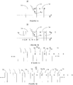
- the most basic building block or converter element 10 of a photon energy converter having a linear structure is comprised of a first layer 12 of type A material having a first atomic number Z 1 and preferably comprising a high atomic number component, such as, for example, a refractory metal or metal oxide.
- the first layer 12 is preferably sandwiched between two layers 14 of type B material having a second atomic number Z 2 differing from the atomic number of the first layer 12 of type A material, and preferably comprising a metal that is typically preferably characterized by a lower atomic number than the atomic number of the first layer 12 of type A material (i.e., Z 2 ⁇ Z 1 ).
- the basic building block 10 can optionally be enhanced by the addition of an insulator layer 16 of type C material.
- converters 11 and 13 include a series or an array of the basic building blocks stacked laterally side-by-side (i.e., face-to-face) until the theoretical maximum aggregate photon path-length spent by the photon in all type A layers 12 is comparable to or larger than the mean free path of the high energy photons v to be absorbed by the type A material.
- one or more layers 14 of type B material interpose adjacent layers 12 of type A material, and, optionally, a layer 16 of type C insulation material interposes adjacent layers 14 of type B material.
- Stacking the building blocks or converter elements 10 side-by-side provides a geometry for the overall structure that is well suited to effectively accommodate the electron emissions caused by the high energy photons v absorbed in the type A material. Because the polarization of photons E , as depicted in Figure 3 , is perpendicular to the direction of propagation of the photon v, the direction of the ejected electron e - is primarily in a plane P e (with an appropriately decaying angular distribution away from that plane, but peaking on that plane) perpendicular to the direction of the propagation of the photons v (but such plane contains the polarization of the photons v).
- the layers 12 and 14 of the converter elements 10 are stacked side-by-side in a direction such that the normal vector to the boundary surfaces between layers is generally orthogonal to the direction of the propagation of the photons v.
- the boundary surfaces between layers can be aligned at a grazing (shallow) angle with the direction of propagation of the incident high-energy photon v.
- each layer 12 of type A material is preferably smaller than or on the order of the length of the mean free path of electrons in such type A material.
- each layer 14 of type B material is preferably larger than or on the order of the length of the mean free path of electrons in the type B material.
- the nanometric arrangement of the layers of these embodiments is reflective of the intrinsic physical principles that the electron mean free path in the type A material, l e (Z 1 ), is not too different from the electron mean free path in the type B material, l e (Z 2 ), while at the same time the photon mean free path in the type A material is much less than its mean free path in the type B material, i.e., l p (Z 1 ) ⁇ l p (Z 2 ).
- typical layer thickness dimensions for these systems include l 1 for type A material equal to approximately 1 nm and l 2 for type B material equal to approximately 100 nm, with l 3 for the optional type C material adjusted to prevent arcing between neighboring layers where necessary.
- l 1 for type A material equal to approximately 1 nm
- l 2 for type B material equal to approximately 100 nm
- l 3 for the optional type C material adjusted to prevent arcing between neighboring layers where necessary.
- these dimensions are less than the gyroradius ⁇ e of the electrons. Therefore, on these length scales the electrons are not magnetized, but their dynamics are primarily in the collisional regime.
- the converter elements 10 or converters 11 and 13 discussed above are also applicable to applications where magnetic fields are absent or negligibly small.
- individual layers 12 and 14 can be connected in a fashion whereby each layer 12 of type A material is connected to one of the nearest layers 14 of type B material as depicted in Figure 1E , or each layer 12 of type A material can be connected to one of the nearest layers 14 of type B material that is separated from it by an insulating layer 16 of type C material as depicted in Figure 1F .
- the electrically coupled layers effectively form nano-batteries and the spontaneously formed electric potential difference is on the order of the kinetic energy of migrating electrons.
- the total voltage available to drive a load is equal to the voltage of an individual nano-battery cell 15 or the sum of the series of nano-battery cells 17 and 19.
- an external circuit 20 comprising a load 22 is coupled to the nano-battery cells 17 and 19, which are depicted as coupled in series but could be coupled in parallel.
- the load 22 may comprise an electrically drivable system or component, an energy storage system, an electrical grid, or the like.
- the steady state voltage can be externally controlled and the thickness of the insulating layer 16 sized accordingly.
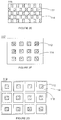
- the basic building block includes a cylindrical tube or shell configuration.
- a cylindrical converter element 110 comprises a cylindrical core 112 of type A material surrounded by a cylindrical tube or shell 114 of type B material.
- a cylindrical tube or shell 114 of type B material As depicted in Figure 2B , it is again possible to optionally surround each shell 114 of type B material with an insulating shell 116 of type C material.
- the same dimensional rules apply to the various thicknesses, i.e., the radius of the cylindrical cores 112 of type A material is less than or on the order of about half of the electron mean free path in type A material, about l e (Z 1 )/2, while the thickness of the shell 114 of type B material is on the order of the electron mean free path in material B, about l e (Z 2 ).
- the advantage of the cylindrical tube or shell arrangement of the converter element 110 is the higher efficiency it affords in capturing the emitted electrons as they are emitted with equal probability over an entire 360° azimuth.
- electrons e - are ejected in a direction primarily in a plane P c (with an appropriately decaying angular distribution away from that plane, but peaking on that plane) perpendicular to the direction of propagation of the photon v and parallel to the polarization ( E ⁇ ) of the photons.
- the ejected electron e - can be directed anywhere about the 360° azimuth and in such case the cylindrical arrangement of the cell leads to higher electron capture in type B material and effectively a higher electron capture efficiency as compared to the linear configurations depicted in Figure 1A through IF.
- the cylindrical building blocks 110 are bundled to form aggregate structures that conform to the same physical size constraints as the linear geometry converter.
- one particular stacking arrangement 111 is depicted in Figure 2C .
- insulating material 116 can fill the void spaces between adjacent converter elements or cells 110.
- Such void space can also serve as a conduit for circulating gas coolants, such as pressurized Helium. This forms an effective means of cooling because the photon absorption by He is negligible over the photon energies of interest.
- Electrical connections are again similar to the linear geometry configurations and likewise afford many different options in connecting the layers or shells 112 and 114 of the building blocks 110.
- Figures 2E, 2F and 2G Alternative geometric configurations are shown in Figures 2E, 2F and 2G.
- Figure 2E shows a staggered linear stacked layered arrangement in which layers 112 of type A material are offset to be positioned adjacent layers 114 of type B material.
- Figure 2F shows a plurality of cores 112 of type A material surround by type B material filing the void spaces 114 between the cores 112. Although shown square shaped, the cores 112 could be circular, oval, or the like.
- Figure 2G is similar to the configuration in Figure 2D with the exception of the core 112 and shell layer 114 being square shaped. In these cases the dimensioning of elements 112, 114 and 116 conforms to the same constraints discussed in Figures 1A through 1C and Figures 2A through 2D .
- the electron dynamics at the edges of the squares are different, but aside from these edge effects the other physical properties are generally similar to the cylindrical cases.
- the basic building block in either geometry, which as described above is made up of up to three kinds of materials, is suitable to spontaneously generate electron separation from the original site of donor atoms, which have been ionized by high-energy photons. This in turn gives rise to the generation of electric voltages between the layers and/or across the optional insulator.
- such an arrangement can be electrically connected to a circuit to do electric work or transmit power from the converter.
- an external voltage bias voltage
- the stacked layers 212 and 214 of type A and B materials, and the optional layer 216 of type C insulation material, of a converter tile or cell 200 are preferably tilted at a grazing (shallow) angle ⁇ to the direction of propagation of the incident high-energy photon v, which, for example, may be on the order of about 1/100 radian.
- Tilting the converter tile 200 also assures adequate cooling of the bombarded type A material and minimizes the thickness of each individual layer 212 of type A material (relative to the mean free path of electrons) as well as the aggregate effective thickness of all layers 212 of type A material in the entire converter assembly. Tilting the converter tile 200 at a grazing angle also causes the electrons to be ejected predominantly perpendicularly to the surface of the type A material. It also reduces the necessary number of repeated layers per tile 200 by a factor of approximately 1/ ⁇ , as the transmission distance in the type A material is enhanced by the same factor over the case where the orientation angle ⁇ of the surface of tile 200 is organized normal to the propagation direction of the incident high energy photon v. It also maximizes the escape of electrons into the adjacent layer of type B material.
- the converter tile 200 depicted in Figures 4A and 4B comprises a plurality of cylindrical converter elements 110 (shown in Figures 2A and 2B ) stacked side by side and tilted at a grazing angle ⁇ .
- the height H of the device needs to extend to orders of length of about one centimeter (1 cm) in the general direction of the predominant photon propagation. This is due to the desire to intercept the entire photon flux with type A material with sufficient aggregate thickness in the photon propagation direction.
- each layer of type B material is typically much greater than the thickness of each layer of type A material (l 1 ⁇ l 2 )
- the total height H of the complete stack of building blocks projected onto the direction of the photon flux needs to be much greater than the mean free path of the particular photons in the type A material to insure that high energy photons encounter type A material over an aggregate distance greater than their mean free path in such material.
- the height of the complete stack of building blocks therefore, should exceed the mean free path of photons in the type A material by a factor of at least l 2 / l 1 or, in the case of inclusion of the insulating layer, by a factor of at least (l 3 + l 2 )/ l 1 .
- the overall arrangement also provides effective cooling of the converter materials as they are heated by photon absorption as well as subsequent electron heating.
- the cooling is facilitated because the total surface area in the present embodiment, as depicted in Figure 4A , is enlarged compared to a simple arrangement of layering the stacks at an orientation angle ⁇ perpendicular to the direction of the incident photon flux by a factor of 1/ ⁇ .
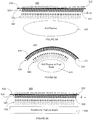
- An assembly 220 of the converter tiles 200 can be arranged along a conforming surface 230 that intercepts and is substantially perpendicular to the photon flux 242 emitted from a given photon flux source 240.
- This configuration provides flexibility and adaptability to a wide spectrum of applications that might require (or benefit from) energy generation from the emitted photon flux.
- Figure 6A shows a plasma containment system 300 that includes a cylindrical chamber 330 having a surface 334 that intercepts and is substantially perpendicular to a photon flux 342 emitted from a source 340 of photon flux shown as hot plasma.
- the containment system 300 further comprises a magnetic field generator 332 positioned along the cylindrical chamber 330 and an array 332 of converter tiles 200 affixed along the surface 334 of the chamber 330. Each of the tiles is oriented at a grazing angle to the direction of propagation of the incident high-energy photons v of the photon flux 342.
- Figure 6B shows a containment system 400 that includes a cylindrical container 430 having a surface 434 that intercepts and is substantially perpendicular to a photon flux 442 emitted from a source 440 of photon flux shown as hot plasma or expend fission fuel rods.
- the containment system 400 further comprises an array 432 of converter tiles 200 affixed about the surface 434 of the container 430. Each of the tiles is oriented at a grazing angle to the direction of propagation of the incident high-energy photons v of the photon flux 442.
- Figure 6C shows a particle acceleration system 500 that includes a cylindrical tube 530 having a surface 534 that intercepts and is substantially perpendicular to a photon flux 542 emitted from a source 540 of photon flux shown as an accelerated particle beam.
- the accelerator system 500 further comprises a magnetic field generator 532 positioned along the cylindrical tube 530 and an array 532 of converter tiles 200 affixed along the surface 534 of the tube 530. Each of the tiles is oriented at a grazing angle to the direction of propagation of the incident high-energy photons v of the photon flux 542.
- the emitted high energy photons encounter type A material over an aggregate distance greater than their mean free path in such material A. This assures their proper absorption by atoms within the type A layers and ultimately amplified conversion of photon current to electron current.
- the type A material densely covers all high energy photon flux exposed surface areas, while at the same time allowing for cooling and electrical connections.
- multiple electrons are emitted from a particular atom in the type A material due to absorption of high-energy photons. This is because an electron that is knocked out from a particular deep electronic inner shell state creates a vacancy, which is quickly filled by the Auger process, which in turn triggers secondary and tertiary Auger processes, or a cascade of processes.
- secondary photon re-emission can trigger further such processes in neighboring atoms. Accordingly, one photon can in principle trigger the aggregate emission of some 100 electrons (and sometimes more). Therefore, this multiple ionization provides double benefits.
- the voltage generated is manageable relative to break down concerns. This provides enhanced conversion of photon energy to electricity (its charge and current), while it also minimizes heating of the target.
- the system serves as an efficacious coolant means by removing most of the deposited photon energy (via electric energy) from the material that sits next to the photon source and readily transports the converted energy away to remote sites not in the vicinity of the radiation.
Landscapes
- Physics & Mathematics (AREA)
- Engineering & Computer Science (AREA)
- General Physics & Mathematics (AREA)
- Condensed Matter Physics & Semiconductors (AREA)
- Electromagnetism (AREA)
- Computer Hardware Design (AREA)
- Microelectronics & Electronic Packaging (AREA)
- Power Engineering (AREA)
- High Energy & Nuclear Physics (AREA)
- General Engineering & Computer Science (AREA)
- Life Sciences & Earth Sciences (AREA)
- Health & Medical Sciences (AREA)
- Molecular Biology (AREA)
- Spectroscopy & Molecular Physics (AREA)
- Sustainable Development (AREA)
- Sustainable Energy (AREA)
- Particle Accelerators (AREA)
- X-Ray Techniques (AREA)
- Optical Modulation, Optical Deflection, Nonlinear Optics, Optical Demodulation, Optical Logic Elements (AREA)
- Physical Or Chemical Processes And Apparatus (AREA)
- Surface Treatment Of Glass (AREA)
- Luminescent Compositions (AREA)
- Analysing Materials By The Use Of Radiation (AREA)
Description
- The embodiments described herein relate generally to photonic energy conversion and, more particularly, to systems and methods that facilitate the conversion of energy from high-energy photons into electricity.
- There exist many well-known devices that convert the energy of photons in the optical range into electricity, such as, e.g., photovoltaic cells ('solar cells'). These devices are generally made up of at least two materials (i.e. silicon-based semiconductors) with different physical properties, such as different electron affinities (see, P. Würfel, The Physics of Solar Cells, 1st Edition, Wiley-VCH (2004)). When one of the materials is illuminated by sunshine, solar photons excite photoelectrons from a valence band into a conduction band, which provides electric mobility. The energy gap between valence and conduction bands is typically on the order of an electron-volt, which is similar to the energy of the incident solar photons. The arrangement of two materials with different electron affinities gives rise to an electric voltage across the material boundary, which may be tapped for electric energy.
- There are, however, no known devices for conversion into electricity of energy from photons operating in the high-energy photon regime such as, e.g., XUV, X and gamma rays. Such devices could be used in a wide range of applications - for example, such devices could be used as energy converters for the conversion of high-energy photons emitted by radioactive materials such as, e.g., spent fission fuel rods, emitted from detonation sources such as, e.g., explosives, and emitted from high temperature plasmas and beams of accelerated particles, and as devices in space applications as power sources, shielding, and the like. Difficulties in providing such devices arise from the great penetrability of high-energy photons through matter, which is a consequence of much less interaction of such photons with matter when compared with visible light, and from the fact that for most materials the mean-free-path of electrons is typically many orders of magnitude shorter than the mean-free-path of high-energy photons. As a consequence of this disparity in mean-free-paths, electrons emitted from an atom in a material used to trap the high-energy photons tend to succumb to recombination while their energy converts to heat within the high-energy photon trapping material.
- Thus, it is desirable to provide systems and methods that would facilitate the conversion of energy from high-energy photons into electricity.
-
US2003019517-A1 discloses an apparatus and method for solar energy production comprising a multi-layer solid-state structure including a photosensitive layer, a thin conductor, a charge separation layer, and a back ohmic conductor, wherein light absorption occurs in a photosensitive layer and the charge carriers produced thereby are transported through the thin conductor through the adjacent potential energy barrier. The open circuit voltage of the solar cell can be manipulated by choosing from among a wide selection of materials making up the thin conductor, the charge separation layer, and the back ohmic layer.US5111099 discloses an apparatus and method for converting radioactive energy into electrical energy, with the apparatus including an outer radioactive protective shell and a radioactive fuel source located within that shell. In their preferred embodiment, three mutually perpendicular magnetic fields are provided to separate alpha and beta particles emitted from the radioactive fuel source and to direct the alpha particles to a first predetermined region of the shell while directing the beta particles to a second predetermined region. An alpha collector is situated adjacent the first region to collect the alpha particles directed to that region, while a beta collector is situated within the second region to collect beta particles directed thereto. Structure is provided to permit removal of gaseous by-product from within the shell, and output leads are provided to utilize the collected alpha and beta particles to create electric current.US2004163942-A1 discloses a plurality of metallic plates arranged alternately so that the main surface of one of the metallic plates is faced to the main surface of the adjacent one of the metallic plates. The metallic plates are classified into two kinds of plates with different thicknesses. Then, energy beams are irradiated perpendicularly onto the main surfaces of the metallic plates to generate an electric energy by interactions between the energy beams and the metallic plates. JPS63182870 discloses a laminated radiation detection element. - The present application provides an energy converter system for converting high energy photon emissions into electrical energy in accordance with the claims which follow.
- The systems and methods described herein may be utilized in a wide range of applications - from energy detection and absorption, to energy conversion of high-energy photons in particle accelerators and from other extremely hot matter (such as high temperature plasmas) and/or detonation sources that emit copious high-energy photons (such as explosives), energy capture of emissions of radioactive nuclear wastes (such as spent fission fuel rods), and space applications (such as power sources, shielding, and the like), as well as other applications readily recognizable to one skilled in the art.
- Other systems, methods, features and advantages of the example embodiments will be or will become apparent to one with skill in the art upon examination of the following figures and detailed description.
- The details of the example embodiments, including structure and operation, may be gleaned in part by study of the accompanying figures, in which like reference numerals refer to like parts. The components in the figures are not necessarily to scale, emphasis instead being placed upon illustrating the principles of the invention. Moreover, all illustrations are intended to convey concepts, where relative sizes, shapes and other detailed attributes may be illustrated schematically rather than literally or precisely.
-
FIGURE 1A is a schematic of a linearly layered nanometric-scaled high-energy photon converter element. -
FIGURE 1B is a schematic of an alternative linearly layered nanometric-scaled high-energy photon converter element. -
FIGURE 1C is a schematic of a high-energy photon converter comprising an array of linearly layered nanometric-scaled converter elements shown inFIGURE 1A . -
FIGURE 1D is a schematic of a high-energy photon converter comprising an array of linearly layered nanometric-scaled converter elements shown inFIGURE 1B . -
FIGURE 1E is a schematic of a high-energy photon converter circuit. -
FIGURE 1F is a schematic of an alternative high-energy photon converter circuit coupled to an external circuit comprising a load. -
FIGURE 2A is a perspective view of a cylindrically layered nanometric-scaled high-energy photon converter element. -
FIGURE 2B is a perspective view of an alternative cylindrically layered nanometric-scaled high-energy photon converter element. -
FIGURE 2C is a perspective view of a high-energy photon converter comprising an array of cylindrically layered nanometric-scaled converter elements shown inFIGURE 2A . -
FIGURE 2D is a end view of a high-energy photon converter comprising an array of cylindrically layered nanometric-scaled converter elements shown inFIGURE 2B . -
FIGURES 2E, 2F and 2G are end views of high-energy photon converters with alternative geometric configurations. -
FIGURE 3 is a diagram illustrating the propagation characteristics of incident high energy photons v and the migrating characteristics of electrons e- that are ejected from their atoms in a layer of material by the incident high-energy photons v. -
FIGURE 4A is a schematic of a converter tile comprising a plurality of linearly stacked layers. -
FIGURE 4B is a perspective view of a converter tile comprising a plurality of linearly stacked layers. -
FIGURE 5 is a schematic showing an assembly of the tiles depicted inFIGURES 4A and 4B arranged along a conforming surface that intercepts and is substantially perpendicular to a photon flux emitted from a photon flux source -
FIGURES 6A, 6B and 6C are schematics showing an assembly of the tiles depicted inFIGURES 4A and 4B arranged along conforming surfaces that intercept and are substantially perpendicular to photon fluxes emitted from photon flux sources. - It should be noted that elements of similar structures or functions are generally represented by like reference numerals for illustrative purpose throughout the figures. It should also be noted that the figures are only intended to facilitate the description of the preferred embodiments.
- Each of the additional features and teachings disclosed below can be utilized separately or in conjunction with other features and teachings to produce systems and methods to facilitate the conversion of energy from high-energy photons into electricity. Representative examples of the present invention, which examples utilize many of these additional features and teachings both separately and in combination, will now be described in further detail with reference to the attached drawings. This detailed description is merely intended to teach a person of skill in the art further details for practicing preferred aspects of the present teachings and is not intended to limit the scope of the invention. Therefore, combinations of features and steps disclosed in the following detail description may not be necessary to practice the invention in the broadest sense, and are instead taught merely to particularly describe representative examples of the present teachings.
- Moreover, the various features of the representative examples and the dependent claims may be combined in ways that are not specifically and explicitly enumerated in order to provide additional useful embodiments of the present teachings. In addition, it is expressly noted that all features disclosed in the description and/or the claims are intended to be disclosed separately and independently from each other for the purpose of original disclosure, as well as for the purpose of restricting the claimed subject matter independent of the compositions of the features in the embodiments and/or the claims. It is also expressly noted that all value ranges or indications of groups of entities disclose every possible intermediate value or intermediate entity for the purpose of original disclosure, as well as for the purpose of restricting the claimed subject matter.
- The embodiments described herein are directed to the conversion of energy from high-energy photons (such as, e.g., photons with energy preferably in a range of about 100 eV or greater) into electricity. The principle underlying the embodiments is based on the ejection of electrons from an atom (including the ejection of deep seated inner shell electrons from an atom of high atomic number (high-Z) materials) by high-energy photons. The ejected electrons carry kinetic energy, which can lead to the migration of the ejected electrons into different regions of a device where the accumulation of the ejected electrons can create an electric potential that can be tapped to drive an external electric circuit. The photon spectrum of interest includes photons preferably in the non-visible regime including, but not limited to, XUV rays, X-rays, gamma rays and the like. The energy of such photons is orders of magnitude larger and, thus, the margin for thermalization is much greater (the theoretical Carnot coefficient is near unity), than the energy of photons in the visible regime. Because of the high incident photon energy, generally 100 eV or greater, the systems and methods described herein are capable of extraordinarily high efficiency of energy conversion, as compared with other standard energy converters of photons, such as photoelectric devices (e.g. solar cells), or devices based on the thermoelectric effect (e.g., Seebeck effect).
- As discussed in further detail below, the systems and methods used to harness this potentially high gain effectively channel the energies of the high-energy photons into an appropriate form of electric energy, which can then be tapped to drive an external circuit, and, thus, cover a wide range of applications, including those where strong magnetic fields are present (such that electron dynamics are characterized by gyromotion across the magnetic fields). As a result, the systems and methods described herein may be utilized in a wide range of applications - from energy detection and absorption, to energy conversion of high-energy photons in particle accelerators, direct energy conversion of high-energy photons from other extremely hot matter (such as high temperature plasmas) and/or detonation sources that emit copious high-energy photons (such as explosives), energy capture of emissions of radioactive nuclear wastes (such as spent fission fuel rods), and space applications (such as power sources, shielding, and the like), as well as other applications readily recognizable to one skilled in the art.
- The systems and methods provided herein utilize a series of layers of materials with differing atomic charges to take advantage of the emission of a large multiplicity of electrons by a single high-energy photon via a cascade of Auger electron emissions. In one embodiment, a high-energy photon converter preferably includes a linearly layered nanometric-scaled wafer made up of a first plurality of layers of materials for absorbing high energy photons and emitting electrons combined with a second plurality of layers of other materials for absorbing or collecting electrons emitted from the first plurality of layers. The materials of the second plurality of layers having an atomic charge number differing from the atomic charge numbers of the materials of the first plurality of layers. In another embodiment, the nanometric-scaled layers are configured in a tubular or shell-like configuration. The nanometric layers facilitate the segregation of photoelectrons from donor atoms. Utilizing these structures, the resultant converter may reduce the power flux incident on materials that would otherwise be directly exposed to high-energy photons, thereby reducing the amount of heating of these materials and may also ameliorate the degradation of the materials that are otherwise subject to severe high-energy photon irradiation damages.
- Turning in detail to the figures, systems and methods for energy conversion of high-energy photons into electricity with high efficiency are illustrated. For purposes of the foregoing discussion, the converter device or devices are assumed to be embedded in strong magnetic fields that can decisively impact the electron orbits. However, as will be evident below, on the characteristic length scales of the device, the electron orbital properties are minimally affected by the magnetic fields (with strengths that are practically attainable) so that the embodiments are equally applicable to applications where there are little or no magnetic fields present, such as, e.g., spent fission fuel rod applications.
- Referring to
Figures 1A through 1F , embodiments of a photon energy converter having a linear structure is shown. As depicted inFigure 1A , the most basic building block orconverter element 10 of a photon energy converter having a linear structure is comprised of afirst layer 12 of type A material having a first atomic number Z1 and preferably comprising a high atomic number component, such as, for example, a refractory metal or metal oxide. Thefirst layer 12 is preferably sandwiched between twolayers 14 of type B material having a second atomic number Z2 differing from the atomic number of thefirst layer 12 of type A material, and preferably comprising a metal that is typically preferably characterized by a lower atomic number than the atomic number of thefirst layer 12 of type A material (i.e., Z2< Z1). As depicted inFigure 1B , thebasic building block 10 can optionally be enhanced by the addition of aninsulator layer 16 of type C material. An exemplary set of types A, B and C materials may include, but is not limited to: A = tungsten (W), B = aluminum (Al), C = insulator such as SiO2. Alternatively, the insulator layer might simply be free flowing Helium that can also act as a coolant. However, one skilled in the art will readily recognize that other materials can be substituted consistent with the present invention. - In preferred embodiments depicted in
Figures 1C and 1D ,converters Figures 1C and 1D , one ormore layers 14 of type B material interposeadjacent layers 12 of type A material, and, optionally, alayer 16 of type C insulation material interposesadjacent layers 14 of type B material. - Stacking the building blocks or
converter elements 10 side-by-side provides a geometry for the overall structure that is well suited to effectively accommodate the electron emissions caused by the high energy photons v absorbed in the type A material. Because the polarization of photonsE , as depicted inFigure 3 , is perpendicular to the direction of propagation of the photon v, the direction of the ejected electron e- is primarily in a plane Pe (with an appropriately decaying angular distribution away from that plane, but peaking on that plane) perpendicular to the direction of the propagation of the photons v (but such plane contains the polarization of the photons v). As depicted inFigures 1A and 1B , thelayers converter elements 10 are stacked side-by-side in a direction such that the normal vector to the boundary surfaces between layers is generally orthogonal to the direction of the propagation of the photons v. In one preferred configuration described below, the boundary surfaces between layers can be aligned at a grazing (shallow) angle with the direction of propagation of the incident high-energy photon v. As a result, the electrons e- that are ejected within thelayers 12 of the type A material from their atoms by the incident high-energy photons v are able to migrate generally orthogonally into the neighboringlayers 14 of type B material. - Central to the principle of each embodiment, and any variation thereof, is the requirement that the emitted photoelectrons e- not be trapped and/or absorbed in the
layer 12 of type A material, but rather be absorbed in thelayer 14 of type B material. To insure that the ejected electrons e- are not trapped within thelayer 12 of type A material and increase the likelihood that the ejected electrons e- escape or migrate from thelayer 12 of type A material into alayer 14 of type B material, the thickness, ℓ1, of eachlayer 12 of type A material is preferably smaller than or on the order of the length of the mean free path of electrons in such type A material. The thickness, ℓ2, of eachlayer 14 of type B material is preferably larger than or on the order of the length of the mean free path of electrons in the type B material. Preferably, the nanometric arrangement of the layers of these embodiments is reflective of the intrinsic physical principles that the electron mean free path in the type A material, ℓe(Z1), is not too different from the electron mean free path in the type B material, ℓe(Z2), while at the same time the photon mean free path in the type A material is much less than its mean free path in the type B material, i.e., ℓp(Z1) << ℓp(Z2). - For example for 100 keV incident photons, typical layer thickness dimensions for these systems include ℓ1 for type A material equal to approximately 1 nm and ℓ2 for type B material equal to approximately 100 nm, with ℓ3 for the optional type C material adjusted to prevent arcing between neighboring layers where necessary. For magnetic fields B up to 10 T, these dimensions are less than the gyroradius ρe of the electrons. Therefore, on these length scales the electrons are not magnetized, but their dynamics are primarily in the collisional regime. As a result, the
converter elements 10 orconverters - The migration into the neighboring
layers 14 of type B material of electrons e- ejected from atoms within thelayers 12 of type A material by the incident high-energy photons v leads to an accumulation of charge and ultimately generates a potential between thelayers Figures 1E and 1F , all type A and type B layers 12 and 14 are connected to circuits such that eachtype A layer 12 andtype B layer 14 acts as an individual electrode. As readily apparent to one skilled in the art, there exists an almost infinite number of options and alternatives to connect the layers or groupings of layers in parallel or serial fashion. The optimal arrangement of such circuitry is advantageously application determinable as a result. For example,individual layers layer 12 of type A material is connected to one of thenearest layers 14 of type B material as depicted inFigure 1E , or eachlayer 12 of type A material can be connected to one of thenearest layers 14 of type B material that is separated from it by an insulatinglayer 16 of type C material as depicted inFigure 1F . In these configurations, the electrically coupled layers effectively form nano-batteries and the spontaneously formed electric potential difference is on the order of the kinetic energy of migrating electrons. The total voltage available to drive a load is equal to the voltage of an individual nano-battery cell 15 or the sum of the series of nano-battery cells Figure 1F , anexternal circuit 20 comprising aload 22 is coupled to the nano-battery cells load 22 may comprise an electrically drivable system or component, an energy storage system, an electrical grid, or the like. - Alternatively, by adjusting the load resistance of the circuit between the electrode layers 12 and 14, the steady state voltage can be externally controlled and the thickness of the insulating
layer 16 sized accordingly. - In another embodiment, the basic building block includes a cylindrical tube or shell configuration. As illustrated in
Figure 2A , acylindrical converter element 110 comprises acylindrical core 112 of type A material surrounded by a cylindrical tube or shell 114 of type B material. As depicted inFigure 2B , it is again possible to optionally surround eachshell 114 of type B material with an insulatingshell 116 of type C material. In this cylindrical configuration the same dimensional rules apply to the various thicknesses, i.e., the radius of thecylindrical cores 112 of type A material is less than or on the order of about half of the electron mean free path in type A material, about ℓe(Z1)/2, while the thickness of theshell 114 of type B material is on the order of the electron mean free path in material B, about ℓe(Z2). - The advantage of the cylindrical tube or shell arrangement of the
converter element 110 is the higher efficiency it affords in capturing the emitted electrons as they are emitted with equal probability over an entire 360° azimuth. As depicted inFigure 3 and described above, electrons e- are ejected in a direction primarily in a plane Pc (with an appropriately decaying angular distribution away from that plane, but peaking on that plane) perpendicular to the direction of propagation of the photon v and parallel to the polarization (E̅ ) of the photons. Depending on the angle of polarization of the photon, the ejected electron e- can be directed anywhere about the 360° azimuth and in such case the cylindrical arrangement of the cell leads to higher electron capture in type B material and effectively a higher electron capture efficiency as compared to the linear configurations depicted inFigure 1A through IF. - Similar to the linear geometry converter described above, the
cylindrical building blocks 110 are bundled to form aggregate structures that conform to the same physical size constraints as the linear geometry converter. As an example, one particular stackingarrangement 111 is depicted inFigure 2C . Alternatively, as depicted inFigure 2D , in another stackingarrangement 113, insulatingmaterial 116 can fill the void spaces between adjacent converter elements orcells 110. Such void space can also serve as a conduit for circulating gas coolants, such as pressurized Helium. This forms an effective means of cooling because the photon absorption by He is negligible over the photon energies of interest. Electrical connections are again similar to the linear geometry configurations and likewise afford many different options in connecting the layers orshells - Alternative geometric configurations are shown in
Figures 2E, 2F and 2G. Figure 2E shows a staggered linear stacked layered arrangement in which layers 112 of type A material are offset to be positionedadjacent layers 114 of type B material.Figure 2F shows a plurality ofcores 112 of type A material surround by type B material filing thevoid spaces 114 between thecores 112. Although shown square shaped, thecores 112 could be circular, oval, or the like.Figure 2G is similar to the configuration inFigure 2D with the exception of thecore 112 andshell layer 114 being square shaped. In these cases the dimensioning ofelements Figures 1A through 1C andFigures 2A through 2D . The electron dynamics at the edges of the squares are different, but aside from these edge effects the other physical properties are generally similar to the cylindrical cases. - The basic building block in either geometry, which as described above is made up of up to three kinds of materials, is suitable to spontaneously generate electron separation from the original site of donor atoms, which have been ionized by high-energy photons. This in turn gives rise to the generation of electric voltages between the layers and/or across the optional insulator. As discussed above, such an arrangement can be electrically connected to a circuit to do electric work or transmit power from the converter. As a further variant, it should be noted that one can also apply an external voltage (bias voltage) between these layers, which provides further control over the electric properties and minimizes the potential for arching across any of the layers.
- Referring to
Figures 4A and 4B , in order to maximize the radiation exposed surface area to insure that the incident high energy photon v is captured by alayer 212 of type A material and does not simply pass through alayer 214 of type B material, thestacked layers optional layer 216 of type C insulation material, of a converter tile orcell 200 are preferably tilted at a grazing (shallow) angle θ to the direction of propagation of the incident high-energy photon v, which, for example, may be on the order of about 1/100 radian. Tilting theconverter tile 200 also assures adequate cooling of the bombarded type A material and minimizes the thickness of eachindividual layer 212 of type A material (relative to the mean free path of electrons) as well as the aggregate effective thickness of alllayers 212 of type A material in the entire converter assembly. Tilting theconverter tile 200 at a grazing angle also causes the electrons to be ejected predominantly perpendicularly to the surface of the type A material. It also reduces the necessary number of repeated layers pertile 200 by a factor of approximately 1/θ, as the transmission distance in the type A material is enhanced by the same factor over the case where the orientation angle Φ of the surface oftile 200 is organized normal to the propagation direction of the incident high energy photon v. It also maximizes the escape of electrons into the adjacent layer of type B material. - In an alternative embodiment, the
converter tile 200 depicted inFigures 4A and 4B comprises a plurality of cylindrical converter elements 110 (shown inFigures 2A and 2B ) stacked side by side and tilted at a grazing angle θ. - Referring to
Figure 4B , in order to effectively absorb most of the high-energy photons with energy on the order of about 100 keV, the height H of the device needs to extend to orders of length of about one centimeter (1 cm) in the general direction of the predominant photon propagation. This is due to the desire to intercept the entire photon flux with type A material with sufficient aggregate thickness in the photon propagation direction. Since the thickness of each layer of type B material is typically much greater than the thickness of each layer of type A material (ℓ1 << ℓ2), the total height H of the complete stack of building blocks projected onto the direction of the photon flux needs to be much greater than the mean free path of the particular photons in the type A material to insure that high energy photons encounter type A material over an aggregate distance greater than their mean free path in such material. The height of the complete stack of building blocks, therefore, should exceed the mean free path of photons in the type A material by a factor of at least ℓ2/ ℓ1 or, in the case of inclusion of the insulating layer, by a factor of at least (ℓ3 + ℓ2)/ ℓ1. - As mentioned above, the overall arrangement also provides effective cooling of the converter materials as they are heated by photon absorption as well as subsequent electron heating. The cooling is facilitated because the total surface area in the present embodiment, as depicted in
Figure 4A , is enlarged compared to a simple arrangement of layering the stacks at an orientation angle Φ perpendicular to the direction of the incident photon flux by a factor of 1/θ. It is also possible to flow pressurized gas coolant through pipes built into the structure or simply connect the stacks to heat sinks. One skilled in the art would readily recognize that there may be many other ways to enhance the cooling and that particular implementations will be dictated by the specific application. - An
assembly 220 of theconverter tiles 200, as depicted inFigure 5 , can be arranged along a conformingsurface 230 that intercepts and is substantially perpendicular to thephoton flux 242 emitted from a givenphoton flux source 240. This configuration provides flexibility and adaptability to a wide spectrum of applications that might require (or benefit from) energy generation from the emitted photon flux. - Other examples of overall geometries of typical applications are depicted in
Figures 6A, 6B and 6C. Figure 6A shows aplasma containment system 300 that includes acylindrical chamber 330 having asurface 334 that intercepts and is substantially perpendicular to aphoton flux 342 emitted from asource 340 of photon flux shown as hot plasma. Thecontainment system 300 further comprises amagnetic field generator 332 positioned along thecylindrical chamber 330 and anarray 332 ofconverter tiles 200 affixed along thesurface 334 of thechamber 330. Each of the tiles is oriented at a grazing angle to the direction of propagation of the incident high-energy photons v of thephoton flux 342.Figure 6B shows acontainment system 400 that includes acylindrical container 430 having asurface 434 that intercepts and is substantially perpendicular to aphoton flux 442 emitted from asource 440 of photon flux shown as hot plasma or expend fission fuel rods. Thecontainment system 400 further comprises an array 432 ofconverter tiles 200 affixed about thesurface 434 of thecontainer 430. Each of the tiles is oriented at a grazing angle to the direction of propagation of the incident high-energy photons v of thephoton flux 442.Figure 6C shows aparticle acceleration system 500 that includes acylindrical tube 530 having asurface 534 that intercepts and is substantially perpendicular to aphoton flux 542 emitted from asource 540 of photon flux shown as an accelerated particle beam. Theaccelerator system 500 further comprises amagnetic field generator 532 positioned along thecylindrical tube 530 and anarray 532 ofconverter tiles 200 affixed along thesurface 534 of thetube 530. Each of the tiles is oriented at a grazing angle to the direction of propagation of the incident high-energy photons v of thephoton flux 542. - In each case the emitted high energy photons encounter type A material over an aggregate distance greater than their mean free path in such material A. This assures their proper absorption by atoms within the type A layers and ultimately amplified conversion of photon current to electron current. Surrounding the flux emitting volume, the type A material densely covers all high energy photon flux exposed surface areas, while at the same time allowing for cooling and electrical connections.
- It should be noted that in accordance with the embodiments provided herein, multiple electrons are emitted from a particular atom in the type A material due to absorption of high-energy photons. This is because an electron that is knocked out from a particular deep electronic inner shell state creates a vacancy, which is quickly filled by the Auger process, which in turn triggers secondary and tertiary Auger processes, or a cascade of processes. In addition, secondary photon re-emission can trigger further such processes in neighboring atoms. Accordingly, one photon can in principle trigger the aggregate emission of some 100 electrons (and sometimes more). Therefore, this multiple ionization provides double benefits. First, it serves to multiply the amount of electrons per original incident photon by a factor of 100 to 1,000, which leads to high current amplification. Second, it serves to reduce the electron energies from tens of keV to mere tens of eV. Thus, the voltage generated is manageable relative to break down concerns. This provides enhanced conversion of photon energy to electricity (its charge and current), while it also minimizes heating of the target. In fact the system serves as an efficacious coolant means by removing most of the deposited photon energy (via electric energy) from the material that sits next to the photon source and readily transports the converted energy away to remote sites not in the vicinity of the radiation.
- The example embodiments provided herein, however, are merely intended as illustrative examples and not to be limiting in any way. Moreover, one skilled in the art will readily recognize that similar systems can be equally adapted to photons of different energies with appropriate modification of parameters.
- In the foregoing specification, the invention has been described with reference to specific embodiments thereof. It will, however, be evident that various modifications and changes may be made thereto without departing from the scope of the invention, which is defined in the appended claims.
Claims (10)
- An energy converter system for converting high energy photon emissions into electrical energy comprising:a high energy photon energy converter for converting high energy photon emissions into electrical energy comprisinga plurality of layers of a first material (12, 212) that is adapted to absorb high energy photons having energies in the range of about 100 eV or greater from a photon flux (242, 342, 442, 542), and to emit electrons ejected from an atom in the first layer of material by a high energy photon having an energy in the range of about 100 eV or greater and absorbed in a layer of the plurality of layers of a first material, each layer of the plurality of layers of a first material having a thickness along the direction of propagation of the ejected electrons that is less than the length of the mean free path of the ejected electrons in the first material, andwherein the plurality of layers of a first material having an aggregate thickness measured along the direction of propagation of a high energy photon that is greater than the length of a mean free path for the high energy photon in the first material, anda plurality of layers of a second material (14, 214) that collects electrons emitted from the plurality of layers of a first material and electrically coupled to the plurality of layers of a first material, each layer of the plurality of layers of a second material having a thickness greater than the length of the mean free path in the second material of the electrons emitted from the first material, wherein each layer of the plurality of layers of a first material interpose adjacent layers of the plurality layers of a second material, andwherein the layers are arranged such, that the direction of propagation of the high energy photons is at a grazing angle to a boundary surface between adjacent layers of the plurality of layers of first and second materials, anda wall (230, 330, 430, 530) surrounding a photon flux source 240, 340, 440, 540) and having a surface that intercepts and is substantially perpendicular to a direction of propagation of the photon flux (242, 342, 442, 542) emitted from the photon flux source, and a plurality of converter tiles (220, 320, 420, 520) covering the surface of the wall, the converter tiles providing the plurality of layers of the first material and the plurality of layers of the second material.
- The system of claim 1 further comprising a plurality of layers of a third material (16, 216) each coupled to an individual layer of the plurality of layers of a second material, the third material comprising an insulator material.
- The system of claim 1 wherein the plurality of layers of the first and second materials are stacked face to face.
- The system of claims 1 - 3 wherein the first material comprises a high atomic charge number component.
- The system of claim 4 wherein the atomic charge number of the second material differs from the atomic charge number of the first.
- The system of claims 1 - 5 wherein the atomic charge number of the second material is lower than the atomic charge number of the first material.
- The system of claims 1 - 6 wherein the first material is configured to absorb the high energy photons which include X, XUV or gamma rays.
- The system of claim 1 - 7 wherein the plurality of layers of the first and second materials are coupled to a circuit having a load (22).
- The converter of claim 8 wherein the load is an electrically drivable component, an electricity storage system or an electricity grid.
- The converter of claims 1 - 9 wherein the plurality of layers of the first and second materials are couplable to a surface (230, 334, 434, 534) that intercepts and is substantially perpendicular to a direction of propagation of a photon flux (242, 342, 442, 542) emitted from a photon flux source (240, 340, 440, 540) and wherein each layer of the the plurality of layers of the first and second materials is oriented at a grazing angle to the direction of propagation of the photon flux.
Applications Claiming Priority (2)
| Application Number | Priority Date | Filing Date | Title |
|---|---|---|---|
| US29328210P | 2010-01-08 | 2010-01-08 | |
| PCT/US2011/020001 WO2011084903A1 (en) | 2010-01-08 | 2011-01-01 | Conversion of high-energy photons into electricity |
Publications (3)
| Publication Number | Publication Date |
|---|---|
| EP2522033A1 EP2522033A1 (en) | 2012-11-14 |
| EP2522033A4 EP2522033A4 (en) | 2016-04-20 |
| EP2522033B1 true EP2522033B1 (en) | 2018-11-14 |
Family
ID=44305761
Family Applications (1)
| Application Number | Title | Priority Date | Filing Date |
|---|---|---|---|
| EP11732017.6A Active EP2522033B1 (en) | 2010-01-08 | 2011-01-01 | Conversion of high-energy photons into electricity |
Country Status (19)
| Country | Link |
|---|---|
| US (3) | US9324897B2 (en) |
| EP (1) | EP2522033B1 (en) |
| JP (3) | JP6097563B2 (en) |
| KR (1) | KR101962974B1 (en) |
| CN (2) | CN102859706B (en) |
| AR (1) | AR079858A1 (en) |
| AU (2) | AU2010339631B2 (en) |
| BR (1) | BR112012016873B1 (en) |
| CA (1) | CA2786590C (en) |
| EA (1) | EA025124B1 (en) |
| ES (1) | ES2705690T3 (en) |
| IL (2) | IL220819A (en) |
| MX (1) | MX2012007991A (en) |
| NZ (1) | NZ601448A (en) |
| SG (1) | SG182383A1 (en) |
| TW (2) | TWI552362B (en) |
| UA (1) | UA111585C2 (en) |
| WO (1) | WO2011084903A1 (en) |
| ZA (1) | ZA201205568B (en) |
Families Citing this family (26)
| Publication number | Priority date | Publication date | Assignee | Title |
|---|---|---|---|---|
| WO2010089670A1 (en) | 2009-02-04 | 2010-08-12 | General Fusion, Inc. | Systems and methods for compressing plasma |
| JP2012524374A (en) | 2009-04-16 | 2012-10-11 | エリック・エイチ・シルバー | Monochromatic X-ray method and apparatus |
| BR112012002147B1 (en) | 2009-07-29 | 2020-12-22 | General Fusion, Inc | systems and methods for plasma compression with projectile recycling |
| ES2705690T3 (en) | 2010-01-08 | 2019-03-26 | Tae Tech Inc | Conversion of high energy photons into electricity |
| EP2891389B1 (en) | 2012-08-29 | 2017-08-02 | General Fusion Inc. | Apparatus for accelerating and compressing plasma |
| KR20230056054A (en) * | 2014-03-03 | 2023-04-26 | 브릴리언트 라이트 파워, 인크. | Photovoltaic power generation systems and methods regarding same |
| US10722219B2 (en) | 2014-06-25 | 2020-07-28 | Mayo Foundation For Medical Education And Research | System and method for quantitative muscle ultrasound for diagnosis of neuromuscular disease |
| US9967963B2 (en) | 2014-08-19 | 2018-05-08 | General Fusion Inc. | System and method for controlling plasma magnetic field |
| US10269463B2 (en) * | 2015-02-03 | 2019-04-23 | The United States Of America As Represented By The Administrator Of Nasa | Nuclear thermionic avalanche cells with thermoelectric (NTAC-TE) generator in tandem mode |
| WO2022187176A1 (en) * | 2021-03-01 | 2022-09-09 | Tae Technologies, Inc. | Carbon negative reactors |
| US11063198B2 (en) | 2016-04-05 | 2021-07-13 | United States Of America As Represented By The Administrator Of Nasa | Metallic junction thermoelectric generator |
| KR20240055138A (en) | 2017-05-19 | 2024-04-26 | 이매진 싸이언티픽, 인크. | Monochromatic x-ray imaging systems and methods |
| CN107783170A (en) * | 2017-09-28 | 2018-03-09 | 摩瑞尔电器(昆山)有限公司 | Using the gamma ray detection equipment of composite structure shell |
| US10811144B2 (en) | 2017-11-06 | 2020-10-20 | General Fusion Inc. | System and method for plasma generation and compression |
| US10886452B2 (en) | 2018-01-25 | 2021-01-05 | United States Of America As Represented By The Administrator Of Nasa | Selective and direct deposition technique for streamlined CMOS processing |
| US10818467B2 (en) * | 2018-02-09 | 2020-10-27 | Imagine Scientific, Inc. | Monochromatic x-ray imaging systems and methods |
| AU2019218240B2 (en) | 2018-02-09 | 2024-09-19 | Imagine Scientific, Inc. | Monochromatic x-ray imaging systems and methods |
| US11037687B2 (en) | 2018-03-13 | 2021-06-15 | United States Of America As Represented By The Administrator Of Nasa | Co-60 breeding reactor tandem with thermionic avalanche cell |
| US11004666B2 (en) | 2018-03-15 | 2021-05-11 | United States Of America As Represented By The Administrator Of Nasa | Portable miniaturized thermionic power cell with multiple regenerative layers |
| US10985676B2 (en) | 2018-03-15 | 2021-04-20 | United States Of America As Represented By The Administrator Of Nasa | High performance electric generators boosted by nuclear electron avalanche (NEA) |
| US11257604B2 (en) | 2018-05-30 | 2022-02-22 | United States Of America As Represented By The Administrator Of Nasa | Multi-layered radio-isotope for enhanced photoelectron avalanche process |
| KR102091228B1 (en) * | 2018-06-05 | 2020-03-19 | 서울방사선서비스주식회사 | System and method for managing quality of dosimeter |
| WO2020056281A1 (en) | 2018-09-14 | 2020-03-19 | Imagine Scientific, Inc. | Monochromatic x-ray component systems and methods |
| US11581104B2 (en) | 2019-05-21 | 2023-02-14 | United States Of America As Represented By The Administrator Of Nasa | Multi-layer structure of nuclear thermionic avalanche cells |
| US20220108814A1 (en) * | 2020-10-01 | 2022-04-07 | Robert W Moses | Surface Flashover and Material Texturing for Multiplying and Collecting Electrons for Nuclear Thermal Avalanche Cells and Nuclear Battery Devices |
| US20220302331A1 (en) * | 2021-03-22 | 2022-09-22 | Matthew Ryan Hankla | Methods, systems, and apparatuses for producing, generating and utilizing power and energy |
Citations (1)
| Publication number | Priority date | Publication date | Assignee | Title |
|---|---|---|---|---|
| JPS63182870A (en) * | 1987-01-26 | 1988-07-28 | Nippon Mining Co Ltd | Laminated radiation detection element |
Family Cites Families (31)
| Publication number | Priority date | Publication date | Assignee | Title |
|---|---|---|---|---|
| US739987A (en) * | 1898-11-11 | 1903-09-29 | American Tobacco Co | Delivery mechanism for cigarette-machines. |
| US2847585A (en) * | 1952-10-31 | 1958-08-12 | Rca Corp | Radiation responsive voltage sources |
| GB761404A (en) * | 1953-06-30 | 1956-11-14 | Rca Corp | Improved methods of and means for converting the energy of nuclear radiations into useful electrical energy |
| US3284241A (en) * | 1962-02-13 | 1966-11-08 | Philco Corp | Photo-emissive device including emitter and insulator of less than mean free path dimensions |
| BE716262A (en) | 1967-07-25 | 1968-11-04 | ||
| US3591860A (en) * | 1968-07-22 | 1971-07-06 | Henry T Sampson | Gamma-electric cell |
| US3821556A (en) * | 1972-02-15 | 1974-06-28 | Nasa | Three mirror glancing incidence system for x ray telescope |
| CH539928A (en) * | 1972-05-26 | 1973-07-31 | Biviator Sa | Nuclear battery |
| US4178524A (en) * | 1976-09-01 | 1979-12-11 | Ritter James C | Radioisotope photoelectric generator |
| JPH065291B2 (en) | 1986-07-02 | 1994-01-19 | 株式会社日立製作所 | Radiation detector |
| US4873555A (en) * | 1987-06-08 | 1989-10-10 | University Of Pittsburgh Of The Commonwealth System Of Higher Education | Intraband quantum well photodetector and associated method |
| US5111099A (en) * | 1990-03-02 | 1992-05-05 | Genesis Energy Systems, Inc. | Apparatus and method for converting radioactive energy into electrical energy |
| JP3126158B2 (en) | 1991-04-10 | 2001-01-22 | 日本放送協会 | Thin film cold cathode |
| GB9415584D0 (en) | 1994-08-02 | 1994-09-21 | Imperial College | Photo detector |
| ATE249094T1 (en) | 1998-06-11 | 2003-09-15 | Petr Viscor | FLAT ELECTRON EMMITTER |
| FR2792418B1 (en) * | 1999-04-15 | 2001-06-01 | Commissariat Energie Atomique | TWO-DIMENSIONAL DETECTOR OF IONIZING RADIATION AND METHOD OF MANUFACTURING THE SAME |
| SE514471C2 (en) | 1999-04-30 | 2001-02-26 | Xcounter Ab | X-ray detector unit with fixed type converter |
| DE60039535D1 (en) * | 2000-10-20 | 2008-08-28 | Josuke Nakata | LICHTEMITTIERDENDE BZW. LIGHT-SENSITIVE SEMICONDUCTOR ARRANGEMENT AND ITS MANUFACTURING METHOD |
| US6774300B2 (en) * | 2001-04-27 | 2004-08-10 | Adrena, Inc. | Apparatus and method for photovoltaic energy production based on internal charge emission in a solid-state heterostructure |
| EP2219049A3 (en) | 2001-06-18 | 2017-12-20 | Wisconsin Alumni Research Foundation | Radiation detector with converters |
| US7485799B2 (en) * | 2002-05-07 | 2009-02-03 | John Michael Guerra | Stress-induced bandgap-shifted semiconductor photoelectrolytic/photocatalytic/photovoltaic surface and method for making same |
| JP3837528B2 (en) * | 2002-12-13 | 2006-10-25 | 国立大学法人名古屋大学 | Power generation method and battery |
| JP3861154B2 (en) | 2003-09-04 | 2006-12-20 | 国立大学法人名古屋大学 | Power generation method and battery |
| CN101042945A (en) * | 2006-07-20 | 2007-09-26 | 永州市健民射线防护设备有限公司 | Environment-friendly type radiation protection composite board |
| TW200812096A (en) * | 2006-08-25 | 2008-03-01 | Kinik Co | Amorphous diamond energy converter |
| CN100501924C (en) * | 2006-12-19 | 2009-06-17 | 华东师范大学 | A making method for the radiant energy conversion chip |
| JP2010517299A (en) * | 2007-01-30 | 2010-05-20 | ソーラスタ インコーポレイテッド | Photocell and method for producing the same |
| WO2008144414A1 (en) | 2007-05-15 | 2008-11-27 | Aeroflex Colorado Springs Inc. | Energy sensitive direct conversion radiation detector |
| WO2009036308A1 (en) | 2007-09-12 | 2009-03-19 | Sub-One Technology | Hybrid photovoltaically active layer and method for forming such a layer |
| FI121828B (en) | 2007-12-04 | 2011-04-29 | Finphys Oy | Radiation detector, method of producing a radiation detector and use of the detector for measuring radiation |
| ES2705690T3 (en) | 2010-01-08 | 2019-03-26 | Tae Tech Inc | Conversion of high energy photons into electricity |
-
2011
- 2011-01-01 ES ES11732017T patent/ES2705690T3/en active Active
- 2011-01-01 CA CA2786590A patent/CA2786590C/en active Active
- 2011-01-01 AU AU2010339631A patent/AU2010339631B2/en active Active
- 2011-01-01 SG SG2012049854A patent/SG182383A1/en unknown
- 2011-01-01 MX MX2012007991A patent/MX2012007991A/en active IP Right Grant
- 2011-01-01 CN CN201180012910.6A patent/CN102859706B/en active Active
- 2011-01-01 CN CN201610882742.0A patent/CN107123692B/en active Active
- 2011-01-01 BR BR112012016873-8A patent/BR112012016873B1/en active IP Right Grant
- 2011-01-01 JP JP2012548054A patent/JP6097563B2/en active Active
- 2011-01-01 NZ NZ601448A patent/NZ601448A/en unknown
- 2011-01-01 EP EP11732017.6A patent/EP2522033B1/en active Active
- 2011-01-01 WO PCT/US2011/020001 patent/WO2011084903A1/en active Application Filing
- 2011-01-01 US US13/521,220 patent/US9324897B2/en active Active
- 2011-01-01 EA EA201290620A patent/EA025124B1/en unknown
- 2011-01-01 KR KR1020127020707A patent/KR101962974B1/en active IP Right Grant
- 2011-01-01 UA UAA201209620A patent/UA111585C2/en unknown
- 2011-01-07 TW TW103137578A patent/TWI552362B/en active
- 2011-01-07 TW TW100100596A patent/TWI463681B/en active
- 2011-01-07 AR ARP110100050 patent/AR079858A1/en active IP Right Grant
-
2012
- 2012-07-08 IL IL220819A patent/IL220819A/en active IP Right Grant
- 2012-07-24 ZA ZA2012/05568A patent/ZA201205568B/en unknown
-
2016
- 2016-02-19 AU AU2016201030A patent/AU2016201030B2/en active Active
- 2016-03-31 US US15/087,283 patent/US9570644B2/en active Active
- 2016-05-24 JP JP2016103082A patent/JP6327722B2/en active Active
- 2016-12-28 US US15/392,769 patent/US9893226B2/en active Active
-
2017
- 2017-01-11 IL IL250054A patent/IL250054B/en active IP Right Grant
- 2017-10-23 JP JP2017204520A patent/JP2018028552A/en not_active Withdrawn
Patent Citations (1)
| Publication number | Priority date | Publication date | Assignee | Title |
|---|---|---|---|---|
| JPS63182870A (en) * | 1987-01-26 | 1988-07-28 | Nippon Mining Co Ltd | Laminated radiation detection element |
Also Published As
Similar Documents
| Publication | Publication Date | Title |
|---|---|---|
| US9893226B2 (en) | Conversion of high-energy photons into electricity | |
| JP2013516624A5 (en) | ||
| US20130015363A1 (en) | Detector, method for manufacturing a detector and imaging apparatus | |
| US4178524A (en) | Radioisotope photoelectric generator | |
| US20130154438A1 (en) | Power-Scalable Betavoltaic Battery | |
| JP5906088B2 (en) | Generator excited by ionizing radiation | |
| US5861701A (en) | Charged-particle powered battery | |
| US20040163942A1 (en) | Method for generating electric power and electric battery | |
| Lee et al. | Vacuum ultraviolet and ultrasoft x‐ray diode detectors for tokamak plasmas | |
| Ronen et al. | Conceptual design of americium nuclear battery for space power applications | |
| Popa-Samil | Meta-material based nuclear structure applications in beamed thrust and space energy harvesting | |
| Klose et al. | X-Ray Multi Camera Tomography System of Wendelstein 7-X | |
| Cho et al. | Characterization and interpretation of the quantum efficiencies of multilayer semiconductor detectors using a new theory | |
| SELMI | 3D sensors for the Insertable B-Layer of the ATLAS experiment at the CERN LHC |
Legal Events
| Date | Code | Title | Description |
|---|---|---|---|
| PUAI | Public reference made under article 153(3) epc to a published international application that has entered the european phase |
Free format text: ORIGINAL CODE: 0009012 |
|
| 17P | Request for examination filed |
Effective date: 20120724 |
|
| AK | Designated contracting states |
Kind code of ref document: A1 Designated state(s): AL AT BE BG CH CY CZ DE DK EE ES FI FR GB GR HR HU IE IS IT LI LT LU LV MC MK MT NL NO PL PT RO RS SE SI SK SM TR |
|
| DAX | Request for extension of the european patent (deleted) | ||
| RA4 | Supplementary search report drawn up and despatched (corrected) |
Effective date: 20160323 |
|
| RIC1 | Information provided on ipc code assigned before grant |
Ipc: H01L 31/00 20060101AFI20160317BHEP Ipc: H01L 31/0352 20060101ALI20160317BHEP Ipc: H01L 31/0725 20120101ALI20160317BHEP Ipc: G21H 1/06 20060101ALI20160317BHEP Ipc: G01T 1/28 20060101ALI20160317BHEP Ipc: G21H 1/04 20060101ALI20160317BHEP Ipc: H01L 31/115 20060101ALI20160317BHEP |
|
| STAA | Information on the status of an ep patent application or granted ep patent |
Free format text: STATUS: EXAMINATION IS IN PROGRESS |
|
| 17Q | First examination report despatched |
Effective date: 20170504 |
|
| RAP1 | Party data changed (applicant data changed or rights of an application transferred) |
Owner name: TAE TECHNOLOGIES, INC. |
|
| GRAP | Despatch of communication of intention to grant a patent |
Free format text: ORIGINAL CODE: EPIDOSNIGR1 |
|
| STAA | Information on the status of an ep patent application or granted ep patent |
Free format text: STATUS: GRANT OF PATENT IS INTENDED |
|
| INTG | Intention to grant announced |
Effective date: 20180607 |
|
| GRAS | Grant fee paid |
Free format text: ORIGINAL CODE: EPIDOSNIGR3 |
|
| GRAA | (expected) grant |
Free format text: ORIGINAL CODE: 0009210 |
|
| STAA | Information on the status of an ep patent application or granted ep patent |
Free format text: STATUS: THE PATENT HAS BEEN GRANTED |
|
| AK | Designated contracting states |
Kind code of ref document: B1 Designated state(s): AL AT BE BG CH CY CZ DE DK EE ES FI FR GB GR HR HU IE IS IT LI LT LU LV MC MK MT NL NO PL PT RO RS SE SI SK SM TR |
|
| REG | Reference to a national code |
Ref country code: GB Ref legal event code: FG4D |
|
| REG | Reference to a national code |
Ref country code: CH Ref legal event code: EP Ref country code: AT Ref legal event code: REF Ref document number: 1065861 Country of ref document: AT Kind code of ref document: T Effective date: 20181115 |
|
| REG | Reference to a national code |
Ref country code: DE Ref legal event code: R096 Ref document number: 602011053862 Country of ref document: DE |
|
| REG | Reference to a national code |
Ref country code: IE Ref legal event code: FG4D |
|
| REG | Reference to a national code |
Ref country code: CH Ref legal event code: NV Representative=s name: IP PARTNERS J. WENGER, CH |
|
| REG | Reference to a national code |
Ref country code: NL Ref legal event code: FP |
|
| REG | Reference to a national code |
Ref country code: LT Ref legal event code: MG4D |
|
| REG | Reference to a national code |
Ref country code: ES Ref legal event code: FG2A Ref document number: 2705690 Country of ref document: ES Kind code of ref document: T3 Effective date: 20190326 |
|
| REG | Reference to a national code |
Ref country code: AT Ref legal event code: MK05 Ref document number: 1065861 Country of ref document: AT Kind code of ref document: T Effective date: 20181114 |
|
| PG25 | Lapsed in a contracting state [announced via postgrant information from national office to epo] |
Ref country code: LV Free format text: LAPSE BECAUSE OF FAILURE TO SUBMIT A TRANSLATION OF THE DESCRIPTION OR TO PAY THE FEE WITHIN THE PRESCRIBED TIME-LIMIT Effective date: 20181114 Ref country code: FI Free format text: LAPSE BECAUSE OF FAILURE TO SUBMIT A TRANSLATION OF THE DESCRIPTION OR TO PAY THE FEE WITHIN THE PRESCRIBED TIME-LIMIT Effective date: 20181114 Ref country code: HR Free format text: LAPSE BECAUSE OF FAILURE TO SUBMIT A TRANSLATION OF THE DESCRIPTION OR TO PAY THE FEE WITHIN THE PRESCRIBED TIME-LIMIT Effective date: 20181114 Ref country code: BG Free format text: LAPSE BECAUSE OF FAILURE TO SUBMIT A TRANSLATION OF THE DESCRIPTION OR TO PAY THE FEE WITHIN THE PRESCRIBED TIME-LIMIT Effective date: 20190214 Ref country code: AT Free format text: LAPSE BECAUSE OF FAILURE TO SUBMIT A TRANSLATION OF THE DESCRIPTION OR TO PAY THE FEE WITHIN THE PRESCRIBED TIME-LIMIT Effective date: 20181114 Ref country code: LT Free format text: LAPSE BECAUSE OF FAILURE TO SUBMIT A TRANSLATION OF THE DESCRIPTION OR TO PAY THE FEE WITHIN THE PRESCRIBED TIME-LIMIT Effective date: 20181114 Ref country code: NO Free format text: LAPSE BECAUSE OF FAILURE TO SUBMIT A TRANSLATION OF THE DESCRIPTION OR TO PAY THE FEE WITHIN THE PRESCRIBED TIME-LIMIT Effective date: 20190214 Ref country code: IS Free format text: LAPSE BECAUSE OF FAILURE TO SUBMIT A TRANSLATION OF THE DESCRIPTION OR TO PAY THE FEE WITHIN THE PRESCRIBED TIME-LIMIT Effective date: 20190314 |
|
| PG25 | Lapsed in a contracting state [announced via postgrant information from national office to epo] |
Ref country code: RS Free format text: LAPSE BECAUSE OF FAILURE TO SUBMIT A TRANSLATION OF THE DESCRIPTION OR TO PAY THE FEE WITHIN THE PRESCRIBED TIME-LIMIT Effective date: 20181114 Ref country code: GR Free format text: LAPSE BECAUSE OF FAILURE TO SUBMIT A TRANSLATION OF THE DESCRIPTION OR TO PAY THE FEE WITHIN THE PRESCRIBED TIME-LIMIT Effective date: 20190215 Ref country code: PT Free format text: LAPSE BECAUSE OF FAILURE TO SUBMIT A TRANSLATION OF THE DESCRIPTION OR TO PAY THE FEE WITHIN THE PRESCRIBED TIME-LIMIT Effective date: 20190314 Ref country code: AL Free format text: LAPSE BECAUSE OF FAILURE TO SUBMIT A TRANSLATION OF THE DESCRIPTION OR TO PAY THE FEE WITHIN THE PRESCRIBED TIME-LIMIT Effective date: 20181114 Ref country code: SE Free format text: LAPSE BECAUSE OF FAILURE TO SUBMIT A TRANSLATION OF THE DESCRIPTION OR TO PAY THE FEE WITHIN THE PRESCRIBED TIME-LIMIT Effective date: 20181114 |
|
| PG25 | Lapsed in a contracting state [announced via postgrant information from national office to epo] |
Ref country code: CZ Free format text: LAPSE BECAUSE OF FAILURE TO SUBMIT A TRANSLATION OF THE DESCRIPTION OR TO PAY THE FEE WITHIN THE PRESCRIBED TIME-LIMIT Effective date: 20181114 Ref country code: PL Free format text: LAPSE BECAUSE OF FAILURE TO SUBMIT A TRANSLATION OF THE DESCRIPTION OR TO PAY THE FEE WITHIN THE PRESCRIBED TIME-LIMIT Effective date: 20181114 Ref country code: DK Free format text: LAPSE BECAUSE OF FAILURE TO SUBMIT A TRANSLATION OF THE DESCRIPTION OR TO PAY THE FEE WITHIN THE PRESCRIBED TIME-LIMIT Effective date: 20181114 |
|
| REG | Reference to a national code |
Ref country code: DE Ref legal event code: R097 Ref document number: 602011053862 Country of ref document: DE |
|
| PG25 | Lapsed in a contracting state [announced via postgrant information from national office to epo] |
Ref country code: SK Free format text: LAPSE BECAUSE OF FAILURE TO SUBMIT A TRANSLATION OF THE DESCRIPTION OR TO PAY THE FEE WITHIN THE PRESCRIBED TIME-LIMIT Effective date: 20181114 Ref country code: EE Free format text: LAPSE BECAUSE OF FAILURE TO SUBMIT A TRANSLATION OF THE DESCRIPTION OR TO PAY THE FEE WITHIN THE PRESCRIBED TIME-LIMIT Effective date: 20181114 Ref country code: SM Free format text: LAPSE BECAUSE OF FAILURE TO SUBMIT A TRANSLATION OF THE DESCRIPTION OR TO PAY THE FEE WITHIN THE PRESCRIBED TIME-LIMIT Effective date: 20181114 Ref country code: MC Free format text: LAPSE BECAUSE OF FAILURE TO SUBMIT A TRANSLATION OF THE DESCRIPTION OR TO PAY THE FEE WITHIN THE PRESCRIBED TIME-LIMIT Effective date: 20181114 Ref country code: RO Free format text: LAPSE BECAUSE OF FAILURE TO SUBMIT A TRANSLATION OF THE DESCRIPTION OR TO PAY THE FEE WITHIN THE PRESCRIBED TIME-LIMIT Effective date: 20181114 |
|
| PLBE | No opposition filed within time limit |
Free format text: ORIGINAL CODE: 0009261 |
|
| STAA | Information on the status of an ep patent application or granted ep patent |
Free format text: STATUS: NO OPPOSITION FILED WITHIN TIME LIMIT |
|
| PG25 | Lapsed in a contracting state [announced via postgrant information from national office to epo] |
Ref country code: LU Free format text: LAPSE BECAUSE OF NON-PAYMENT OF DUE FEES Effective date: 20190101 |
|
| REG | Reference to a national code |
Ref country code: BE Ref legal event code: MM Effective date: 20190131 |
|
| 26N | No opposition filed |
Effective date: 20190815 |
|
| PG25 | Lapsed in a contracting state [announced via postgrant information from national office to epo] |
Ref country code: SI Free format text: LAPSE BECAUSE OF FAILURE TO SUBMIT A TRANSLATION OF THE DESCRIPTION OR TO PAY THE FEE WITHIN THE PRESCRIBED TIME-LIMIT Effective date: 20181114 |
|
| PG25 | Lapsed in a contracting state [announced via postgrant information from national office to epo] |
Ref country code: BE Free format text: LAPSE BECAUSE OF NON-PAYMENT OF DUE FEES Effective date: 20190131 |
|
| PG25 | Lapsed in a contracting state [announced via postgrant information from national office to epo] |
Ref country code: TR Free format text: LAPSE BECAUSE OF FAILURE TO SUBMIT A TRANSLATION OF THE DESCRIPTION OR TO PAY THE FEE WITHIN THE PRESCRIBED TIME-LIMIT Effective date: 20181114 |
|
| PG25 | Lapsed in a contracting state [announced via postgrant information from national office to epo] |
Ref country code: MT Free format text: LAPSE BECAUSE OF NON-PAYMENT OF DUE FEES Effective date: 20190101 |
|
| PG25 | Lapsed in a contracting state [announced via postgrant information from national office to epo] |
Ref country code: CY Free format text: LAPSE BECAUSE OF FAILURE TO SUBMIT A TRANSLATION OF THE DESCRIPTION OR TO PAY THE FEE WITHIN THE PRESCRIBED TIME-LIMIT Effective date: 20181114 |
|
| PG25 | Lapsed in a contracting state [announced via postgrant information from national office to epo] |
Ref country code: HU Free format text: LAPSE BECAUSE OF FAILURE TO SUBMIT A TRANSLATION OF THE DESCRIPTION OR TO PAY THE FEE WITHIN THE PRESCRIBED TIME-LIMIT; INVALID AB INITIO Effective date: 20110101 |
|
| PG25 | Lapsed in a contracting state [announced via postgrant information from national office to epo] |
Ref country code: MK Free format text: LAPSE BECAUSE OF FAILURE TO SUBMIT A TRANSLATION OF THE DESCRIPTION OR TO PAY THE FEE WITHIN THE PRESCRIBED TIME-LIMIT Effective date: 20181114 |
|
| P01 | Opt-out of the competence of the unified patent court (upc) registered |
Effective date: 20230519 |
|
| PGFP | Annual fee paid to national office [announced via postgrant information from national office to epo] |
Ref country code: NL Payment date: 20231123 Year of fee payment: 14 |
|
| PGFP | Annual fee paid to national office [announced via postgrant information from national office to epo] |
Ref country code: GB Payment date: 20231116 Year of fee payment: 14 |
|
| PGFP | Annual fee paid to national office [announced via postgrant information from national office to epo] |
Ref country code: IE Payment date: 20231123 Year of fee payment: 14 Ref country code: FR Payment date: 20231122 Year of fee payment: 14 |
|
| PGFP | Annual fee paid to national office [announced via postgrant information from national office to epo] |
Ref country code: ES Payment date: 20240208 Year of fee payment: 14 |
|
| PGFP | Annual fee paid to national office [announced via postgrant information from national office to epo] |
Ref country code: DE Payment date: 20231121 Year of fee payment: 14 Ref country code: CH Payment date: 20240201 Year of fee payment: 14 |
|
| PGFP | Annual fee paid to national office [announced via postgrant information from national office to epo] |
Ref country code: IT Payment date: 20231212 Year of fee payment: 14 |