EP2521879B1 - Circuit board support structure having fixed circuit board connection device - Google Patents
Circuit board support structure having fixed circuit board connection device Download PDFInfo
- Publication number
- EP2521879B1 EP2521879B1 EP10810795.4A EP10810795A EP2521879B1 EP 2521879 B1 EP2521879 B1 EP 2521879B1 EP 10810795 A EP10810795 A EP 10810795A EP 2521879 B1 EP2521879 B1 EP 2521879B1
- Authority
- EP
- European Patent Office
- Prior art keywords
- circuit board
- connection device
- connection structure
- lighting unit
- support structure
- Prior art date
- Legal status (The legal status is an assumption and is not a legal conclusion. Google has not performed a legal analysis and makes no representation as to the accuracy of the status listed.)
- Active
Links
- 230000037361 pathway Effects 0.000 claims description 14
- 238000004891 communication Methods 0.000 claims description 11
- 238000000034 method Methods 0.000 description 14
- 239000000463 material Substances 0.000 description 8
- 230000008901 benefit Effects 0.000 description 7
- 238000009429 electrical wiring Methods 0.000 description 6
- 230000006870 function Effects 0.000 description 5
- 230000005855 radiation Effects 0.000 description 5
- 230000013011 mating Effects 0.000 description 3
- 239000004065 semiconductor Substances 0.000 description 3
- 239000000853 adhesive Substances 0.000 description 2
- 230000001070 adhesive effect Effects 0.000 description 2
- 238000005516 engineering process Methods 0.000 description 2
- 229920000642 polymer Polymers 0.000 description 2
- 230000004044 response Effects 0.000 description 2
- 238000012546 transfer Methods 0.000 description 2
- OKTJSMMVPCPJKN-UHFFFAOYSA-N Carbon Chemical compound [C] OKTJSMMVPCPJKN-UHFFFAOYSA-N 0.000 description 1
- CWYNVVGOOAEACU-UHFFFAOYSA-N Fe2+ Chemical compound [Fe+2] CWYNVVGOOAEACU-UHFFFAOYSA-N 0.000 description 1
- DGAQECJNVWCQMB-PUAWFVPOSA-M Ilexoside XXIX Chemical compound C[C@@H]1CC[C@@]2(CC[C@@]3(C(=CC[C@H]4[C@]3(CC[C@@H]5[C@@]4(CC[C@@H](C5(C)C)OS(=O)(=O)[O-])C)C)[C@@H]2[C@]1(C)O)C)C(=O)O[C@H]6[C@@H]([C@H]([C@@H]([C@H](O6)CO)O)O)O.[Na+] DGAQECJNVWCQMB-PUAWFVPOSA-M 0.000 description 1
- 238000003491 array Methods 0.000 description 1
- 229910052799 carbon Inorganic materials 0.000 description 1
- 238000006243 chemical reaction Methods 0.000 description 1
- 230000000694 effects Effects 0.000 description 1
- 229910052736 halogen Inorganic materials 0.000 description 1
- 150000002367 halogens Chemical class 0.000 description 1
- 238000005286 illumination Methods 0.000 description 1
- 238000002329 infrared spectrum Methods 0.000 description 1
- 238000002347 injection Methods 0.000 description 1
- 239000007924 injection Substances 0.000 description 1
- 238000012423 maintenance Methods 0.000 description 1
- QSHDDOUJBYECFT-UHFFFAOYSA-N mercury Chemical compound [Hg] QSHDDOUJBYECFT-UHFFFAOYSA-N 0.000 description 1
- 229910001507 metal halide Inorganic materials 0.000 description 1
- 150000005309 metal halides Chemical class 0.000 description 1
- 238000012986 modification Methods 0.000 description 1
- 230000004048 modification Effects 0.000 description 1
- 230000003287 optical effect Effects 0.000 description 1
- 230000008439 repair process Effects 0.000 description 1
- 235000019553 satiation Nutrition 0.000 description 1
- 229910052708 sodium Inorganic materials 0.000 description 1
- 239000011734 sodium Substances 0.000 description 1
- 238000005476 soldering Methods 0.000 description 1
- 239000007787 solid Substances 0.000 description 1
- 238000001228 spectrum Methods 0.000 description 1
- 238000002211 ultraviolet spectrum Methods 0.000 description 1
- 238000001429 visible spectrum Methods 0.000 description 1
- 238000003466 welding Methods 0.000 description 1
Images


Classifications
-
- F—MECHANICAL ENGINEERING; LIGHTING; HEATING; WEAPONS; BLASTING
- F21—LIGHTING
- F21V—FUNCTIONAL FEATURES OR DETAILS OF LIGHTING DEVICES OR SYSTEMS THEREOF; STRUCTURAL COMBINATIONS OF LIGHTING DEVICES WITH OTHER ARTICLES, NOT OTHERWISE PROVIDED FOR
- F21V19/00—Fastening of light sources or lamp holders
- F21V19/001—Fastening of light sources or lamp holders the light sources being semiconductors devices, e.g. LEDs
- F21V19/003—Fastening of light source holders, e.g. of circuit boards or substrates holding light sources
- F21V19/004—Fastening of light source holders, e.g. of circuit boards or substrates holding light sources by deformation of parts or snap action mountings, e.g. using clips
-
- F—MECHANICAL ENGINEERING; LIGHTING; HEATING; WEAPONS; BLASTING
- F21—LIGHTING
- F21V—FUNCTIONAL FEATURES OR DETAILS OF LIGHTING DEVICES OR SYSTEMS THEREOF; STRUCTURAL COMBINATIONS OF LIGHTING DEVICES WITH OTHER ARTICLES, NOT OTHERWISE PROVIDED FOR
- F21V19/00—Fastening of light sources or lamp holders
- F21V19/001—Fastening of light sources or lamp holders the light sources being semiconductors devices, e.g. LEDs
- F21V19/003—Fastening of light source holders, e.g. of circuit boards or substrates holding light sources
- F21V19/0055—Fastening of light source holders, e.g. of circuit boards or substrates holding light sources by screwing
-
- F—MECHANICAL ENGINEERING; LIGHTING; HEATING; WEAPONS; BLASTING
- F21—LIGHTING
- F21V—FUNCTIONAL FEATURES OR DETAILS OF LIGHTING DEVICES OR SYSTEMS THEREOF; STRUCTURAL COMBINATIONS OF LIGHTING DEVICES WITH OTHER ARTICLES, NOT OTHERWISE PROVIDED FOR
- F21V23/00—Arrangement of electric circuit elements in or on lighting devices
- F21V23/001—Arrangement of electric circuit elements in or on lighting devices the elements being electrical wires or cables
-
- F—MECHANICAL ENGINEERING; LIGHTING; HEATING; WEAPONS; BLASTING
- F21—LIGHTING
- F21V—FUNCTIONAL FEATURES OR DETAILS OF LIGHTING DEVICES OR SYSTEMS THEREOF; STRUCTURAL COMBINATIONS OF LIGHTING DEVICES WITH OTHER ARTICLES, NOT OTHERWISE PROVIDED FOR
- F21V23/00—Arrangement of electric circuit elements in or on lighting devices
- F21V23/06—Arrangement of electric circuit elements in or on lighting devices the elements being coupling devices, e.g. connectors
-
- F—MECHANICAL ENGINEERING; LIGHTING; HEATING; WEAPONS; BLASTING
- F21—LIGHTING
- F21V—FUNCTIONAL FEATURES OR DETAILS OF LIGHTING DEVICES OR SYSTEMS THEREOF; STRUCTURAL COMBINATIONS OF LIGHTING DEVICES WITH OTHER ARTICLES, NOT OTHERWISE PROVIDED FOR
- F21V27/00—Cable-stowing arrangements structurally associated with lighting devices, e.g. reels
-
- F—MECHANICAL ENGINEERING; LIGHTING; HEATING; WEAPONS; BLASTING
- F21—LIGHTING
- F21Y—INDEXING SCHEME ASSOCIATED WITH SUBCLASSES F21K, F21L, F21S and F21V, RELATING TO THE FORM OR THE KIND OF THE LIGHT SOURCES OR OF THE COLOUR OF THE LIGHT EMITTED
- F21Y2105/00—Planar light sources
- F21Y2105/10—Planar light sources comprising a two-dimensional array of point-like light-generating elements
- F21Y2105/14—Planar light sources comprising a two-dimensional array of point-like light-generating elements characterised by the overall shape of the two-dimensional array
-
- F—MECHANICAL ENGINEERING; LIGHTING; HEATING; WEAPONS; BLASTING
- F21—LIGHTING
- F21Y—INDEXING SCHEME ASSOCIATED WITH SUBCLASSES F21K, F21L, F21S and F21V, RELATING TO THE FORM OR THE KIND OF THE LIGHT SOURCES OR OF THE COLOUR OF THE LIGHT EMITTED
- F21Y2115/00—Light-generating elements of semiconductor light sources
- F21Y2115/10—Light-emitting diodes [LED]
Definitions
- the present invention is directed generally to a circuit board support structure having a circuit board connection device fixedly received thereon. More particularly, various inventive methods and apparatus disclosed herein relate to a circuit board support structure having a circuit board connection device fixedly received thereon, wherein the circuit board connection device is configured to be removably mated with a corresponding socket connection device of a circuit board.
- LEDs light-emitting diodes
- Functional advantages and benefits of LEDs include high energy conversion and optical efficiency, durability, lower operating costs, and many others. Recent advances in LED technology have provided efficient and robust full-spectrum lighting sources that enable a variety of lighting effects in many applications.
- lighting fixtures have been designed that implement LEDs to reap one or more of the advantages and benefits of LEDs.
- some lighting fixtures have been designed that implement a plurality of LEDs arranged on one or more circuit boards. Each circuit board is attached to a desired support structure in the lighting fixture. Electrical connections (e.g. connections from a power supply and/or a controller) to the circuit board are then made.
- the electrical connections may be made by mating a loose female connector extending from a power source and/or controller, for example, to a corresponding male connector fixed on the circuit board. While such lighting fixtures enable an electrical connection to the circuit board to be made, they require a user to manipulate wires and/or connectors in order to create the electrical connection.
- circuit board support structure having a circuit board connection device fixedly received thereon that is configured to be mated with a corresponding fixed socket connection device of a circuit board, thereby reducing the need for a user to manipulate wires when installing and/or removing the circuit board.
- US 2009/0146561 discloses a lighting unit comprising a mounting base comprising a socket connection device, and a LED package comprising a plug connection device.
- the present disclosure is directed to inventive methods and apparatus for a circuit board support structure having a circuit board connection device fixedly received thereon, and, more particularly, various inventive methods and apparatus disclosed herein relate to a circuit board support structure having a circuit board connection device fixedly received thereon that is configured to be removably mated with a corresponding socket connection device of a circuit board.
- the circuit board support structure may have a circuit board connection device fixedly received thereon.
- the circuit board connection device may be configured to mate with a corresponding socket connection device coupled to a circuit board and when the circuit board connection device mates with the socket connection device, the circuit board may be adjacent the circuit board support structure.
- the circuit board connection device may be configured to mate with a corresponding socket connection device coupled to a circuit board and when the circuit board connection device mates with the socket connection device, the circuit board may be adjacent the circuit board support structure.
- the circuit board connection device may be configured to mate with a corresponding socket connection device coupled to a circuit board and when the circuit board connection device mates
- the support structure may be implemented in a lighting unit having at least one circuit board having at least one light source coupled thereto.
- the light source may be a solid state light source such as, for example, an LED.
- the present disclosure may reduce the need for a user to manipulate wires when installing and/or removing a circuit board and may enable a circuit board to be appropriately aligned with respect to the circuit board support structure.
- a lighting unit is provided according to claim 1.
- circuit board connection structure is oriented substantially perpendicular to the circuit board when the socket connection structure is mated with the circuit board connection structure. In some versions of these embodiments the power supply connection structure is fully received in the connection device recess.
- the lighting unit further includes a wire pathway formed in the circuit board support structure and in communication with the power supply connection structure.
- the wire pathway is a recess extending from the connection device recess.
- at least a portion of the wire pathway extends beneath the printed circuit board when the socket connection structure is mated with the circuit board connection structure.
- the socket connection structure is accessible through a through-board opening provided in the circuit board.
- the socket connection structure includes at least two prongs extending into the through-board opening.
- at least a portion of the circuit board connection structure extends through the through-board opening when the socket connection structure is mated with the circuit board connection structure.
- the socket connection structure is accessible through a through-board opening provided in the circuit board.
- the power supply connection structure is oriented substantially perpendicular to the circuit board connection structure.
- a wire pathway is formed in the circuit board support structure and is in communication with the power supply connection structure.
- the term "LED” should be understood to include any electroluminescent diode or other type of carrier injection/junction-based system that is capable of generating radiation in response to an electric signal.
- the term LED includes, but is not limited to, various semiconductor-based structures that emit light in response to current, light emitting polymers, organic light emitting diodes (OLEDs), electroluminescent strips, and the like.
- the term LED refers to light emitting diodes of all types (including semi-conductor and organic light emitting diodes) that may be configured to generate radiation in one or more of the infrared spectrum, ultraviolet spectrum, and various portions of the visible spectrum (generally including radiation wavelengths from approximately 400 nanometers to approximately 700 nanometers). It should also be understood that the term LED does not limit the physical and/or electrical package type of an LED.
- light source should be understood to refer to any one or more of a variety of radiation sources, including, but not limited to, LED-based sources (including one or more LEDs as defined above), incandescent sources (e.g., filament lamps, halogen lamps), fluorescent sources, phosphorescent sources, high-intensity discharge sources (e.g., sodium vapor, mercury vapor, and metal halide lamps), lasers, other types of electroluminescent sources, pyro-luminescent sources (e.g., flames), candle-luminescent sources (e.g., gas mantles, carbon arc radiation sources), photo-luminescent sources (e.g., gaseous discharge sources), cathode luminescent sources using electronic satiation, galvano-luminescent sources, crystallo-luminescent sources, kine-luminescent sources, thermo-luminescent sources, triboluminescent sources, sonoluminescent sources, radioluminescent sources, and luminescent polymers.
- LED-based sources including one or more
- the term "lighting fixture” is used herein to refer to an implementation or arrangement of one or more lighting units in a particular form factor, assembly, or package.
- the term “lighting unit” is used herein to refer to an apparatus including one or more light sources of same or different types.
- a given lighting unit may have any one of a variety of mounting arrangements for the light source(s), enclosure/housing arrangements and shapes, and/or electrical and mechanical connection configurations. Additionally, a given lighting unit optionally may be associated with (e.g., include, be coupled to and/or packaged together with) various other components (e.g., control circuitry) relating to the operation of the light source(s).
- An "LED-based lighting unit” refers to a lighting unit that includes one or more LED-based light sources as discussed above, alone or in combination with other non LED-based light sources.
- controller is used herein generally to describe various apparatus relating to the operation of one or more light sources.
- a controller can be implemented in numerous ways (e.g., such as with dedicated hardware) to perform various functions discussed herein.
- a "processor” is one example of a controller which employs one or more microprocessors that may be programmed using software (e.g., microcode) to perform various functions discussed herein.
- a controller may be implemented with or without employing a processor, and also may be implemented as a combination of dedicated hardware to perform some functions and a processor (e.g., one or more programmed microprocessors and associated circuitry) to perform other functions. Examples of controller components that may be employed in various embodiments of the present disclosure include, but are not limited to, conventional microprocessors, application specific integrated circuits (ASICs), and field-programmable gate arrays (FPGAs).
- ASICs application specific integrated circuits
- FPGAs field-programmable gate arrays
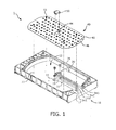
- FIG. 1 through FIG. 4 various aspects of a first embodiment of a lighting unit 1 having a first embodiment of a circuit board support structure 10 are shown.
- a circuit board connection device 20 of the circuit board support structure 10 is shown exploded away from the circuit board support structure 10 in FIG. 1 and is shown unexploded and in a fixed position in FIG. 2 .
- the circuit board support structure 10 may be attached to or placed within a separate housing to create a lighting fixture. Alternatively, the circuit board support structure 10 may form all or part of a lighting fixture housing.
- the circuit board support structure 10 includes a substantially planar circuit board support area 12. Sidewalls surround the circuit board support area 12 and include heat dissipating structure extending therefrom.
- connection device recess 14 is formed in the circuit board support area 12 and includes a pair of fastener apertures 15.
- the circuit board connection device 20 may be fixedly received in the connection device recess 14 by inserting fasteners 25 through fastener openings 26A and 26B (see FIG. 3 ) of circuit board connection device 20 and securing the fasteners 25 in fastener apertures 15.
- the circuit board connection device 20 may be otherwise fixedly received in the connection device recess 14.
- the connection device 20 may be attached using mechanical affixation methods, including, but not limited to adhesives, welding, soldering, prongs, fasteners, and/or structure that may extend from connection device 20 and/or circuit board support area 12.
- a wire pathway 16 extends from the connection device recess 14 toward an opening 17 provided through the circuit board support structure 10.
- the wire pathway 16 is sized to allow wires 34A-D to pass thethrough.
- the wires 34A-D are in electrical communication with the circuit board connection device 20 and may be placed in electrical communication with one or more power supplies and/or controllers.
- the circuit board support structure 10 may be coupled to a housing in communication with opening 17.
- the housing may optionally be coupled to circuit board support structure 10.
- the wires 34A-D may pass through the opening 17 and into the housing where they may be connected to one or more power supplies and/or controllers within the housing.
- wires 34A-B may be coupled to a first LED driver within the housing and wires 34C-D may be coupled to a second LED driver within the housing.
- wires 34A-B may be coupled to a first LED driver within the housing and wires 34C-D may be coupled to a controller that sends electrical signals to alter one or more characteristics of the LEDs 46.
- more or less than four wires 34A-D may be provided and circuit board connection device 20 may optionally be modified to accommodate more or less wires.
- a circuit board 40 of the lighting unit 1 is shown exploded away from the circuit board support structure 10 in both FIG. 1 and FIG. 2 .
- the circuit board 40 has a through-board socket connection device 50 that is shown exploded away from a through-board opening 44 of the circuit board 40 in FIG. 1 and unexploded in a fixed position over the through-board opening 44 in FIG. 2 .
- the circuit board 40 includes a first side 41, a second side opposite the first side 41, and a plurality of LEDs 46.
- the LEDs 46 are mounted to the first side 41 of the circuit board 40 and are in electrical connectivity with the socket connection device 50.
- the socket connection device 50 of the circuit board 40 is removably mateable with the circuit board connection device 20 of the circuit board support structure 10.
- the circuit board 40 When the socket connection device 50 is mated with the circuit board connection device 20, the circuit board 40 is adjacent the circuit board support area 12 of the circuit board support structure 10 and is appropriately aligned with respect to the circuit board support structure 10. Additionally, when the socket connection device 50 is mated with the circuit board connection device 20, they are electrically connected with one another. As a result, LEDs 46 and/or other electronics of circuit board 40 may be electrically connected to a power supply and/or controller via the connection between the socket connection device 50 (which may be electrically connected to LEDs 46 or other electronics of the circuit board 40) and circuit board connection device 20 (which may be electrically connected to a power supply and/or a controller).
- the circuit board 40 may contact the circuit board support area 12 of the circuit board support structure 10 when the socket connection device 50 is mated with the circuit board connection device 20. Contact between the circuit board 40 and the circuit board support area 12 may, in some embodiments, enable heat transfer between the circuit board 40 and the circuit board support area 12 and/or may help reduce movement of the circuit board 40. In some embodiments a material, such as, for example, a heat transfer material may be interposed between the circuit board 40 and the support area 12. In some embodiments the support area 12 may take on alternative configurations.
- the support area 12 may contain one or more recesses in addition to the connection device recess 14 and/or the wire pathway 16 such as, for example, a plurality of troughs extending underneath the circuit board 40, a trough extending along the periphery of the circuit board 40, a trough extending under a majority of the circuit board 40, and/or a plurality of selectively placed recesses.
- the support area 12 may contain one or more protrusions extending therefrom such as, for example, a plurality of bumps extending therefrom and/or one or more alignment notches extending therefrom.
- fasteners 43 may be inserted through apertures in the circuit board 40 and fastened into corresponding fastener apertures 13 of the circuit board support structure 10 to further secure circuit board 40 to the circuit board support structure 10.
- the circuit board 40 may be secured to the circuit board support structure 10 solely via mating between the socket connection device 50 and the circuit board connection device 20.
- the circuit board 40 may be further secured to the circuit board support structure 10 using alternative fixation methods.
- alternative mechanical affixation apparatus may be used, including, but not limited to, prongs, fasteners, clips, depending structure and the like that extend from circuit board 40 and/or circuit board support structure 10 and interface with corresponding structure of the other of circuit board 40 and/or circuit board support structure 10.
- alternative mechanical affixation apparatus may include one or more magnets in or coupled to circuit board 40 and/or circuit board support structure 10 that interact with one or more corresponding magnets or ferrous material in or coupled to the other of circuit board 40 and/or circuit board support structure 10.
- the circuit board connection device 20 has circuit board connection structure that includes female circuit board connection apertures 22A-D that are configured to receive and be electrically connected with corresponding male protrusions such as, for example, male protrusions 52A-D (shown in FIG. 4 ) of socket connection device 50.
- the circuit board connection device 20 also has power supply connection structure that includes female power supply connection apertures 24A-D that are in electrical communication with respective of circuit board connection apertures 22A-D.
- the power supply connection apertures 24A-D are configured to receive and be electrically connected with electrical wiring such as, for example, electrical wiring 34A-D (shown in FIG.
- the power supply connection apertures 24A-D are oriented substantially perependicular to the circuit board connection apertures 22A-D.
- the depicted power supply connection apertures 22A-D may employ any desired apparatus and method for securing electrical wires thereto.
- one or more quick connection apparatus e.g. one or more arms that engage the electrical wire when inserted, a spring loaded contact point that engages the electrical wire
- a crimped connection e.g. one or more arms that engage the electrical wire when inserted, a spring loaded contact point that engages the electrical wire
- a soldered connection e.g. one or more crimped connection, and/or a soldered connection
- Fastener openings 26A and 26B are provided through respective of support wings 25A and 25B and, as described in additional detail herein, may be used in conjunction with fasteners to fixedly secure the circuit board connection device 20.
- Alignment protrusions 28A and 28B are provided on opposed sides of the circuit board connection device 20 and interact with alignment slots 58A and 58B (shown in FIG. 4 ) of socket connection device 50 to help provide proper alignment between circuit board connection device 20 and socket connection device 50.
- the depicted circuit board connection apertures 22A-D are oriented substantially perpendicular to the support surface 12 and to the circuit board 40 when the socket connection device 50 is mated with the circuit board connection device 20.
- the circuit board connection apertures 22A-D extend above a plane generally defined by the support surface 12 and will extend into and through the through-board opening 44 when the socket connection device 20 is mated with the circuit board connection device 20.
- the circuit board connection device 20 may be designed such that the circuit board connection apertures 22A-D do not extend through (and potentially not even into) the through the through-board opening 44 when the socket connection device 50 is mated with the circuit board connection device 20.
- the power supply connection apertures 24A-D are oriented substantially parallel to the support surface 12 and the direction of the wire pathway 16.
- the power supply connection apertures 24A-D are also oriented substantially parallel to the circuit board 40 when the socket connection device 50 is mated with the circuit board connection device 20.
- the socket connection device 50 of the circuit board 40 is shown in additional detail.
- the socket connection device 50 is a through-board connection device, meaning that it connects with the circuit board connection device 20 via an opening provided through a circuit board such as, for example, the through-board opening 44 through circuit board 40.
- the through-board opening 44 may be non-centrally provided on the circuit board 40 and may optionally be provided along the periphery of the circuit board 40.
- Connection structure of the socket connection device 50 and/or connection structure of the circuit board connection device 20 may extend into and/or through the through-board opening 44 to create the mated connection between the two.
- the socket connection device 50 has male socket connecting prongs 52A-D extending downwardly therefrom that are in electrical communication with corresponding of circuit board leads 54A-D.
- the socket connecting prongs 52A-D are configured to be received in and in electrical connectivity with corresponding circuit board connection apertures 22A-D of circuit board connection device 20.
- Circuit board leads 54A-D are configured to be soldered to and in electrical connectivity with corresponding leads of the circuit board 40 that are in electrical communication with one or more LEDs 46 of the circuit board 40.
- the circuit board leads 54A-D may be configured to be otherwise be connected with corresponding leads of the circuit board 40.
- a wall 53 is provided about socket connecting prongs 52A-D and may help minimize unintended contact between socket connecting prongs 52A-D and other items and/or may help align socket connection device 50 with the circuit board connection device 20.
- Side flange 55 and front flange 56 extend perpendicularly from the shielding wall 53 and are substantially coplanar with one another. The side flange 55 and/or the front flange 56 may interact with first side 41 of the circuit board 40 to help align and/or secure the socket connection device 50 to the circuit board 40.
- the side flange 55 and front flange 56 may contact the first side 41 of the circuit board 40 to ensure the socket connecting prongs 52A-D are at a desired location with respect to the through-board opening 44.
- an adhesive may be interposed between the side flange 55 and/or the front flange 56 and the first side 41 of the circuit board 40 to thereby fix the socket connection device 50 to the circuit board 40.
- the socket connecting prongs 52A-D extend into the through-board opening 44 when the socket connection device 50 is mated with the circuit board connection device 20, but not completely through the through-board opening 44.
- the socket connection device 50 may be designed such that the socket connecting prongs 52A-D would not extend into the through-board opening 44 when the socket connection device 50 is mated with the circuit board connection device 20 or, alternatively may be designed such that the socket connecting prongs 52A-D would extend completely through through-board opening 44.
- connection structure depicted in conjunction with circuit board connection device 20 is female connection structure and the connection structure depicted in conjunction with socket connection device 50 is shown as being male connection structure.
- connection structure of circuit board connection device 20 may be male connection structure and/or some or all of the connection structure of socket connection device 50 may be female connection structure.
- FIG. 5 and FIG. 6 illustrate a perspective section view of a portion of a second embodiment of a circuit board support structure 110 having a circuit board support area 112 and a connection device recess 114.
- a circuit board connection device 120 is fixedly rececived in the connection device recess 114.
- Female circuit board connection apertures 122A-C are visible in the section view and are in electrical communication with respective of female power supply connection apertures, of which power supply connection aperture 124C is visible.
- the power supply connection apertures are electrically connected with respective of electrical wiring 134A-C and are also in electrical connectivity with circuit board connection apertures 22A-C. Electrical wiring 134C is visible extending into power supply connection aperture 124C.
- structure may optionally be included in power supply connection aperture 124C to contact and/or retain electrical wiring 134C.
- a circuit board 140 is also shown and includes a first side 141, a second side 142, and a through-board opening 144.
- a socket connection device 150 is in a fixed position over the through-board opening 144 and extends into, but not completely through the through-board opening 144.
- the socket connection device 150 includes male prongs 152A-C that are in electrical connectivity with circuit board leads 154A-C.
- the circuit board leads 154A-C are in electrical communication with electronics of the circuit board 140 via corresponding leads of the circuit board 140.
- the socket connection device 150 of the circuit board 140 is removably mateable with the circuit board connection device 120 of the circuit board support structure 110.
- the socket connection device 150 and the circuit board connection device 120 are shown unattached and spaced apart from one another in FIG. 5 .
- socket connection device 150 and the circuit board connection device 120 are shown mated with one another.
- the circuit board 140 is adjacent the circuit board support area 112 of the circuit board support structure 110.
- the circuit board connection apertures 122A-C extend into and through the through board opening 144.
- FIG. 7 illustrates a second embodiment of a socket connection device 250.
- Socket connection device 250 and socket connection device 50 are similar to one another and like reference numerals refer to like parts of the two.
- Socket connection device 250 does differ from socket connection device 50 in that it features a socket connection hood 259 that is provided atop circuit board leads 254A-D.
- Socket connection hood 259 minimizes the likelihood of unintended electrical contact with circuit board leads 254A-D.
- FIG. 8 illustrates an exploded view of an additional embodiment of a lighting unit 801.
- Lighting unit 801 is similar to lighting unit 1 and like reference numerals refer to like parts of the two.
- lighting unit 801 varies from lighting unit 1 in several respects.
- circuit board 840 is approximately half the size of circuit board 40 and features approximately half the amount of LEDs 846.
- socket connection device 850 is provided through a through-board opening along the periphery of the circuit board 840.
- no fastener apertures are provided in circuit board support structure 810 and circuit board 840 will be secured solely through the mating of socket connection device 850 and circuit board connection device 820.
- wires 834A-D do not extend through a hole in circuit board support structure 810, but, rather, remain in wire pathway 816 until reaching respective electrical connections with an LED driver 877 and a controller 878 that are mounted to the circuit board support structure 810. Also, for example, wires 834A-D and wire pathway 816 do not extend underneath of circuit board 840 after socket connection device 850 is mated with circuit board connection device 820.
- inventive embodiments are presented by way of example only and that, within the scope of the appended claims and equivalents thereto, inventive embodiments may be practiced otherwise than as specifically described and claimed.
- inventive embodiments of the present disclosure are directed to each individual feature, system, article, material, kit, and/or method described herein.
- a reference to "A and/or B", when used in conjunction with open-ended language such as “comprising” can refer, in one embodiment, to A only (optionally including elements other than B); in another embodiment, to B only (optionally including elements other than A); in yet another embodiment, to both A and B (optionally including other elements); etc.
- the phrase "at least one,” in reference to a list of one or more elements, should be understood to mean at least one element selected from any one or more of the elements in the list of elements, but not necessarily including at least one of each and every element specifically listed within the list of elements and not excluding any combinations of elements in the list of elements.
- This definition also allows that elements may optionally be present other than the elements specifically identified within the list of elements to which the phrase "at least one" refers, whether related or unrelated to those elements specifically identified.
- At least one of A and B can refer, in one embodiment, to at least one, optionally including more than one, A, with no B present (and optionally including elements other than B); in another embodiment, to at least one, optionally including more than one, B, with no A present (and optionally including elements other than A); in yet another embodiment, to at least one, optionally including more than one, A, and at least one, optionally including more than one, B (and optionally including other elements); etc.
Landscapes
- Engineering & Computer Science (AREA)
- General Engineering & Computer Science (AREA)
- Non-Portable Lighting Devices Or Systems Thereof (AREA)
- Arrangement Of Elements, Cooling, Sealing, Or The Like Of Lighting Devices (AREA)
- Fastening Of Light Sources Or Lamp Holders (AREA)
- Combinations Of Printed Boards (AREA)
- Coupling Device And Connection With Printed Circuit (AREA)
Applications Claiming Priority (2)
| Application Number | Priority Date | Filing Date | Title |
|---|---|---|---|
| US29235110P | 2010-01-05 | 2010-01-05 | |
| PCT/IB2010/055780 WO2011083382A1 (en) | 2010-01-05 | 2010-12-13 | Circuit board support structure having fixed circuit board connection device |
Publications (2)
| Publication Number | Publication Date |
|---|---|
| EP2521879A1 EP2521879A1 (en) | 2012-11-14 |
| EP2521879B1 true EP2521879B1 (en) | 2015-04-29 |
Family
ID=43857772
Family Applications (1)
| Application Number | Title | Priority Date | Filing Date |
|---|---|---|---|
| EP10810795.4A Active EP2521879B1 (en) | 2010-01-05 | 2010-12-13 | Circuit board support structure having fixed circuit board connection device |
Country Status (10)
| Country | Link |
|---|---|
| US (1) | US8827494B2 (ko) |
| EP (1) | EP2521879B1 (ko) |
| JP (1) | JP2013516728A (ko) |
| KR (1) | KR20120112733A (ko) |
| CN (1) | CN102686940B (ko) |
| CA (1) | CA2786358A1 (ko) |
| MX (1) | MX2012007799A (ko) |
| RU (1) | RU2533210C2 (ko) |
| TW (1) | TW201139926A (ko) |
| WO (1) | WO2011083382A1 (ko) |
Families Citing this family (5)
| Publication number | Priority date | Publication date | Assignee | Title |
|---|---|---|---|---|
| JP5828079B2 (ja) * | 2011-08-30 | 2015-12-02 | パナソニックIpマネジメント株式会社 | 照明装置及び照明システム |
| CN103322472A (zh) * | 2013-06-04 | 2013-09-25 | 中山市迪克力照明电器有限公司 | 一种高压ac ic照明灯 |
| US10310173B2 (en) | 2015-05-18 | 2019-06-04 | Sharp Kabushiki Kaisha | Lighting device and display device |
| CN115803562A (zh) | 2020-06-11 | 2023-03-14 | 昕诺飞控股有限公司 | 包括led模块的灯或灯具 |
| CN111795370A (zh) * | 2020-07-04 | 2020-10-20 | 泰兴市龙腾电子有限公司 | 一种具有固定的电路板连接装置的电路板支撑结构 |
Family Cites Families (8)
| Publication number | Priority date | Publication date | Assignee | Title |
|---|---|---|---|---|
| CN1464953A (zh) * | 2001-08-09 | 2003-12-31 | 松下电器产业株式会社 | Led照明装置和卡型led照明光源 |
| JP2007059930A (ja) * | 2001-08-09 | 2007-03-08 | Matsushita Electric Ind Co Ltd | Led照明装置およびカード型led照明光源 |
| JP3989794B2 (ja) * | 2001-08-09 | 2007-10-10 | 松下電器産業株式会社 | Led照明装置およびled照明光源 |
| US7766518B2 (en) * | 2005-05-23 | 2010-08-03 | Philips Solid-State Lighting Solutions, Inc. | LED-based light-generating modules for socket engagement, and methods of assembling, installing and removing same |
| JP2009117228A (ja) * | 2007-11-08 | 2009-05-28 | Aitec System:Kk | 照明装置 |
| CN101459162B (zh) * | 2007-12-11 | 2010-12-08 | 富士迈半导体精密工业(上海)有限公司 | 固态发光器件 |
| KR101584726B1 (ko) * | 2008-09-01 | 2016-01-13 | 삼성전자주식회사 | 발광모듈 |
| FR2938047A1 (fr) | 2008-10-31 | 2010-05-07 | Mpe Solutions | Dispositif de connexion pour une source lumineuse utilisant des leds |
-
2010
- 2010-12-13 TW TW099143555A patent/TW201139926A/zh unknown
- 2010-12-13 RU RU2012133435/12A patent/RU2533210C2/ru active
- 2010-12-13 MX MX2012007799A patent/MX2012007799A/es active IP Right Grant
- 2010-12-13 US US13/519,422 patent/US8827494B2/en active Active
- 2010-12-13 WO PCT/IB2010/055780 patent/WO2011083382A1/en active Application Filing
- 2010-12-13 KR KR1020127020485A patent/KR20120112733A/ko not_active Application Discontinuation
- 2010-12-13 EP EP10810795.4A patent/EP2521879B1/en active Active
- 2010-12-13 CA CA2786358A patent/CA2786358A1/en not_active Abandoned
- 2010-12-13 CN CN201080060690.XA patent/CN102686940B/zh active Active
- 2010-12-13 JP JP2012546528A patent/JP2013516728A/ja active Pending
Also Published As
| Publication number | Publication date |
|---|---|
| TW201139926A (en) | 2011-11-16 |
| RU2533210C2 (ru) | 2014-11-20 |
| JP2013516728A (ja) | 2013-05-13 |
| CN102686940A (zh) | 2012-09-19 |
| US20120300462A1 (en) | 2012-11-29 |
| CN102686940B (zh) | 2016-12-21 |
| CA2786358A1 (en) | 2011-07-14 |
| EP2521879A1 (en) | 2012-11-14 |
| KR20120112733A (ko) | 2012-10-11 |
| WO2011083382A1 (en) | 2011-07-14 |
| US8827494B2 (en) | 2014-09-09 |
| RU2012133435A (ru) | 2014-02-20 |
| MX2012007799A (es) | 2012-08-03 |
Similar Documents
| Publication | Publication Date | Title |
|---|---|---|
| US8235549B2 (en) | Solid state lighting assembly | |
| EP2333405B1 (en) | Socket assembly with a thermal management structure | |
| JP5682953B2 (ja) | Ledソケット組立体 | |
| US20160123569A1 (en) | Modular luminaire system | |
| EP2521879B1 (en) | Circuit board support structure having fixed circuit board connection device | |
| EP2423570A2 (en) | LED light module | |
| JP5968299B2 (ja) | 点灯装置及び他の電気装置のためのインタフェイス及び製造方法 | |
| US9997909B2 (en) | Surge protection device | |
| JP2012022987A (ja) | 光源モジュール及び照明装置 | |
| CN207635030U (zh) | 快装光源模组及灯具 | |
| JP6471887B2 (ja) | 発光装置およびそれを用いた照明器具 | |
| US9000672B2 (en) | Connector with surge protection structure | |
| EP3111136B1 (en) | Fixture and led system with same | |
| KR101791149B1 (ko) | Led 조명 램프 | |
| JP2017174568A (ja) | 光源ユニット及び照明器具 | |
| JP2017174569A (ja) | 光源ユニット及び照明器具 | |
| KR101544907B1 (ko) | Led 조명 장치 및 이에 적용되는 커넥팅 구조 | |
| US20190331324A1 (en) | Clamping bracket for a driver of a lighting fixture | |
| CN206073000U (zh) | 安装件及安装组件 | |
| US8498098B2 (en) | System for removably retaining a voltage converting device | |
| KR20230119485A (ko) | 등기구용 광원 모듈 | |
| JP2018010734A (ja) | 端子装置、端子部材、光源ユニット及び照明器具 |
Legal Events
| Date | Code | Title | Description |
|---|---|---|---|
| PUAI | Public reference made under article 153(3) epc to a published international application that has entered the european phase |
Free format text: ORIGINAL CODE: 0009012 |
|
| 17P | Request for examination filed |
Effective date: 20120806 |
|
| AK | Designated contracting states |
Kind code of ref document: A1 Designated state(s): AL AT BE BG CH CY CZ DE DK EE ES FI FR GB GR HR HU IE IS IT LI LT LU LV MC MK MT NL NO PL PT RO RS SE SI SK SM TR |
|
| DAX | Request for extension of the european patent (deleted) | ||
| RAP1 | Party data changed (applicant data changed or rights of an application transferred) |
Owner name: KONINKLIJKE PHILIPS N.V. |
|
| GRAP | Despatch of communication of intention to grant a patent |
Free format text: ORIGINAL CODE: EPIDOSNIGR1 |
|
| INTG | Intention to grant announced |
Effective date: 20141124 |
|
| GRAS | Grant fee paid |
Free format text: ORIGINAL CODE: EPIDOSNIGR3 |
|
| GRAA | (expected) grant |
Free format text: ORIGINAL CODE: 0009210 |
|
| AK | Designated contracting states |
Kind code of ref document: B1 Designated state(s): AL AT BE BG CH CY CZ DE DK EE ES FI FR GB GR HR HU IE IS IT LI LT LU LV MC MK MT NL NO PL PT RO RS SE SI SK SM TR |
|
| REG | Reference to a national code |
Ref country code: GB Ref legal event code: FG4D |
|
| REG | Reference to a national code |
Ref country code: CH Ref legal event code: EP |
|
| REG | Reference to a national code |
Ref country code: AT Ref legal event code: REF Ref document number: 724641 Country of ref document: AT Kind code of ref document: T Effective date: 20150515 |
|
| REG | Reference to a national code |
Ref country code: IE Ref legal event code: FG4D |
|
| REG | Reference to a national code |
Ref country code: DE Ref legal event code: R096 Ref document number: 602010024362 Country of ref document: DE Effective date: 20150611 |
|
| REG | Reference to a national code |
Ref country code: NL Ref legal event code: VDEP Effective date: 20150429 |
|
| REG | Reference to a national code |
Ref country code: AT Ref legal event code: MK05 Ref document number: 724641 Country of ref document: AT Kind code of ref document: T Effective date: 20150429 |
|
| REG | Reference to a national code |
Ref country code: LT Ref legal event code: MG4D |
|
| PG25 | Lapsed in a contracting state [announced via postgrant information from national office to epo] |
Ref country code: NL Free format text: LAPSE BECAUSE OF FAILURE TO SUBMIT A TRANSLATION OF THE DESCRIPTION OR TO PAY THE FEE WITHIN THE PRESCRIBED TIME-LIMIT Effective date: 20150429 |
|
| PG25 | Lapsed in a contracting state [announced via postgrant information from national office to epo] |
Ref country code: FI Free format text: LAPSE BECAUSE OF FAILURE TO SUBMIT A TRANSLATION OF THE DESCRIPTION OR TO PAY THE FEE WITHIN THE PRESCRIBED TIME-LIMIT Effective date: 20150429 Ref country code: LT Free format text: LAPSE BECAUSE OF FAILURE TO SUBMIT A TRANSLATION OF THE DESCRIPTION OR TO PAY THE FEE WITHIN THE PRESCRIBED TIME-LIMIT Effective date: 20150429 Ref country code: PT Free format text: LAPSE BECAUSE OF FAILURE TO SUBMIT A TRANSLATION OF THE DESCRIPTION OR TO PAY THE FEE WITHIN THE PRESCRIBED TIME-LIMIT Effective date: 20150831 Ref country code: NO Free format text: LAPSE BECAUSE OF FAILURE TO SUBMIT A TRANSLATION OF THE DESCRIPTION OR TO PAY THE FEE WITHIN THE PRESCRIBED TIME-LIMIT Effective date: 20150729 Ref country code: ES Free format text: LAPSE BECAUSE OF FAILURE TO SUBMIT A TRANSLATION OF THE DESCRIPTION OR TO PAY THE FEE WITHIN THE PRESCRIBED TIME-LIMIT Effective date: 20150429 Ref country code: HR Free format text: LAPSE BECAUSE OF FAILURE TO SUBMIT A TRANSLATION OF THE DESCRIPTION OR TO PAY THE FEE WITHIN THE PRESCRIBED TIME-LIMIT Effective date: 20150429 |
|
| PG25 | Lapsed in a contracting state [announced via postgrant information from national office to epo] |
Ref country code: LV Free format text: LAPSE BECAUSE OF FAILURE TO SUBMIT A TRANSLATION OF THE DESCRIPTION OR TO PAY THE FEE WITHIN THE PRESCRIBED TIME-LIMIT Effective date: 20150429 Ref country code: GR Free format text: LAPSE BECAUSE OF FAILURE TO SUBMIT A TRANSLATION OF THE DESCRIPTION OR TO PAY THE FEE WITHIN THE PRESCRIBED TIME-LIMIT Effective date: 20150730 Ref country code: AT Free format text: LAPSE BECAUSE OF FAILURE TO SUBMIT A TRANSLATION OF THE DESCRIPTION OR TO PAY THE FEE WITHIN THE PRESCRIBED TIME-LIMIT Effective date: 20150429 Ref country code: IS Free format text: LAPSE BECAUSE OF FAILURE TO SUBMIT A TRANSLATION OF THE DESCRIPTION OR TO PAY THE FEE WITHIN THE PRESCRIBED TIME-LIMIT Effective date: 20150829 Ref country code: RS Free format text: LAPSE BECAUSE OF FAILURE TO SUBMIT A TRANSLATION OF THE DESCRIPTION OR TO PAY THE FEE WITHIN THE PRESCRIBED TIME-LIMIT Effective date: 20150429 |
|
| REG | Reference to a national code |
Ref country code: FR Ref legal event code: PLFP Year of fee payment: 6 |
|
| PG25 | Lapsed in a contracting state [announced via postgrant information from national office to epo] |
Ref country code: EE Free format text: LAPSE BECAUSE OF FAILURE TO SUBMIT A TRANSLATION OF THE DESCRIPTION OR TO PAY THE FEE WITHIN THE PRESCRIBED TIME-LIMIT Effective date: 20150429 Ref country code: DK Free format text: LAPSE BECAUSE OF FAILURE TO SUBMIT A TRANSLATION OF THE DESCRIPTION OR TO PAY THE FEE WITHIN THE PRESCRIBED TIME-LIMIT Effective date: 20150429 |
|
| REG | Reference to a national code |
Ref country code: DE Ref legal event code: R097 Ref document number: 602010024362 Country of ref document: DE |
|
| PG25 | Lapsed in a contracting state [announced via postgrant information from national office to epo] |
Ref country code: PL Free format text: LAPSE BECAUSE OF FAILURE TO SUBMIT A TRANSLATION OF THE DESCRIPTION OR TO PAY THE FEE WITHIN THE PRESCRIBED TIME-LIMIT Effective date: 20150429 Ref country code: RO Free format text: LAPSE BECAUSE OF NON-PAYMENT OF DUE FEES Effective date: 20150429 Ref country code: SK Free format text: LAPSE BECAUSE OF FAILURE TO SUBMIT A TRANSLATION OF THE DESCRIPTION OR TO PAY THE FEE WITHIN THE PRESCRIBED TIME-LIMIT Effective date: 20150429 Ref country code: CZ Free format text: LAPSE BECAUSE OF FAILURE TO SUBMIT A TRANSLATION OF THE DESCRIPTION OR TO PAY THE FEE WITHIN THE PRESCRIBED TIME-LIMIT Effective date: 20150429 |
|
| PLBE | No opposition filed within time limit |
Free format text: ORIGINAL CODE: 0009261 |
|
| STAA | Information on the status of an ep patent application or granted ep patent |
Free format text: STATUS: NO OPPOSITION FILED WITHIN TIME LIMIT |
|
| 26N | No opposition filed |
Effective date: 20160201 |
|
| PG25 | Lapsed in a contracting state [announced via postgrant information from national office to epo] |
Ref country code: IT Free format text: LAPSE BECAUSE OF FAILURE TO SUBMIT A TRANSLATION OF THE DESCRIPTION OR TO PAY THE FEE WITHIN THE PRESCRIBED TIME-LIMIT Effective date: 20150429 |
|
| PG25 | Lapsed in a contracting state [announced via postgrant information from national office to epo] |
Ref country code: BE Free format text: LAPSE BECAUSE OF NON-PAYMENT OF DUE FEES Effective date: 20151231 Ref country code: SI Free format text: LAPSE BECAUSE OF FAILURE TO SUBMIT A TRANSLATION OF THE DESCRIPTION OR TO PAY THE FEE WITHIN THE PRESCRIBED TIME-LIMIT Effective date: 20150429 |
|
| PG25 | Lapsed in a contracting state [announced via postgrant information from national office to epo] |
Ref country code: MC Free format text: LAPSE BECAUSE OF FAILURE TO SUBMIT A TRANSLATION OF THE DESCRIPTION OR TO PAY THE FEE WITHIN THE PRESCRIBED TIME-LIMIT Effective date: 20150429 Ref country code: LU Free format text: LAPSE BECAUSE OF FAILURE TO SUBMIT A TRANSLATION OF THE DESCRIPTION OR TO PAY THE FEE WITHIN THE PRESCRIBED TIME-LIMIT Effective date: 20151213 |
|
| REG | Reference to a national code |
Ref country code: CH Ref legal event code: PL |
|
| PG25 | Lapsed in a contracting state [announced via postgrant information from national office to epo] |
Ref country code: BE Free format text: LAPSE BECAUSE OF FAILURE TO SUBMIT A TRANSLATION OF THE DESCRIPTION OR TO PAY THE FEE WITHIN THE PRESCRIBED TIME-LIMIT Effective date: 20150429 |
|
| REG | Reference to a national code |
Ref country code: IE Ref legal event code: MM4A |
|
| PG25 | Lapsed in a contracting state [announced via postgrant information from national office to epo] |
Ref country code: LI Free format text: LAPSE BECAUSE OF NON-PAYMENT OF DUE FEES Effective date: 20151231 Ref country code: CH Free format text: LAPSE BECAUSE OF NON-PAYMENT OF DUE FEES Effective date: 20151231 Ref country code: IE Free format text: LAPSE BECAUSE OF NON-PAYMENT OF DUE FEES Effective date: 20151213 |
|
| REG | Reference to a national code |
Ref country code: GB Ref legal event code: 732E Free format text: REGISTERED BETWEEN 20161006 AND 20161012 |
|
| REG | Reference to a national code |
Ref country code: FR Ref legal event code: PLFP Year of fee payment: 7 |
|
| REG | Reference to a national code |
Ref country code: DE Ref legal event code: R081 Ref document number: 602010024362 Country of ref document: DE Owner name: SIGNIFY HOLDING B.V., NL Free format text: FORMER OWNER: KONINKLIJKE PHILIPS N.V., EINDHOVEN, NL Ref country code: DE Ref legal event code: R082 Ref document number: 602010024362 Country of ref document: DE Representative=s name: MEISSNER BOLTE PATENTANWAELTE RECHTSANWAELTE P, DE Ref country code: DE Ref legal event code: R081 Ref document number: 602010024362 Country of ref document: DE Owner name: PHILIPS LIGHTING HOLDING B.V., NL Free format text: FORMER OWNER: KONINKLIJKE PHILIPS N.V., EINDHOVEN, NL |
|
| PG25 | Lapsed in a contracting state [announced via postgrant information from national office to epo] |
Ref country code: BG Free format text: LAPSE BECAUSE OF FAILURE TO SUBMIT A TRANSLATION OF THE DESCRIPTION OR TO PAY THE FEE WITHIN THE PRESCRIBED TIME-LIMIT Effective date: 20150429 Ref country code: SM Free format text: LAPSE BECAUSE OF FAILURE TO SUBMIT A TRANSLATION OF THE DESCRIPTION OR TO PAY THE FEE WITHIN THE PRESCRIBED TIME-LIMIT Effective date: 20150429 Ref country code: HU Free format text: LAPSE BECAUSE OF FAILURE TO SUBMIT A TRANSLATION OF THE DESCRIPTION OR TO PAY THE FEE WITHIN THE PRESCRIBED TIME-LIMIT; INVALID AB INITIO Effective date: 20101213 |
|
| PG25 | Lapsed in a contracting state [announced via postgrant information from national office to epo] |
Ref country code: CY Free format text: LAPSE BECAUSE OF FAILURE TO SUBMIT A TRANSLATION OF THE DESCRIPTION OR TO PAY THE FEE WITHIN THE PRESCRIBED TIME-LIMIT Effective date: 20150429 Ref country code: SE Free format text: LAPSE BECAUSE OF FAILURE TO SUBMIT A TRANSLATION OF THE DESCRIPTION OR TO PAY THE FEE WITHIN THE PRESCRIBED TIME-LIMIT Effective date: 20150429 |
|
| PG25 | Lapsed in a contracting state [announced via postgrant information from national office to epo] |
Ref country code: MT Free format text: LAPSE BECAUSE OF FAILURE TO SUBMIT A TRANSLATION OF THE DESCRIPTION OR TO PAY THE FEE WITHIN THE PRESCRIBED TIME-LIMIT Effective date: 20150429 |
|
| REG | Reference to a national code |
Ref country code: FR Ref legal event code: PLFP Year of fee payment: 8 |
|
| PG25 | Lapsed in a contracting state [announced via postgrant information from national office to epo] |
Ref country code: TR Free format text: LAPSE BECAUSE OF FAILURE TO SUBMIT A TRANSLATION OF THE DESCRIPTION OR TO PAY THE FEE WITHIN THE PRESCRIBED TIME-LIMIT Effective date: 20150429 Ref country code: MK Free format text: LAPSE BECAUSE OF FAILURE TO SUBMIT A TRANSLATION OF THE DESCRIPTION OR TO PAY THE FEE WITHIN THE PRESCRIBED TIME-LIMIT Effective date: 20150429 |
|
| PG25 | Lapsed in a contracting state [announced via postgrant information from national office to epo] |
Ref country code: AL Free format text: LAPSE BECAUSE OF FAILURE TO SUBMIT A TRANSLATION OF THE DESCRIPTION OR TO PAY THE FEE WITHIN THE PRESCRIBED TIME-LIMIT Effective date: 20150429 |
|
| RIC2 | Information provided on ipc code assigned after grant |
Ipc: F21V 23/06 20060101ALI20110725BHEP Ipc: F21V 19/00 20060101AFI20110725BHEP Ipc: F21Y 101/02 20000101ALI20110725BHEP |
|
| REG | Reference to a national code |
Ref country code: DE Ref legal event code: R082 Ref document number: 602010024362 Country of ref document: DE Representative=s name: MEISSNER BOLTE PATENTANWAELTE RECHTSANWAELTE P, DE Ref country code: DE Ref legal event code: R081 Ref document number: 602010024362 Country of ref document: DE Owner name: SIGNIFY HOLDING B.V., NL Free format text: FORMER OWNER: PHILIPS LIGHTING HOLDING B.V., EINDHOVEN, NL |
|
| P01 | Opt-out of the competence of the unified patent court (upc) registered |
Effective date: 20230421 |
|
| PGFP | Annual fee paid to national office [announced via postgrant information from national office to epo] |
Ref country code: GB Payment date: 20231219 Year of fee payment: 14 |
|
| PGFP | Annual fee paid to national office [announced via postgrant information from national office to epo] |
Ref country code: FR Payment date: 20231226 Year of fee payment: 14 |
|
| PGFP | Annual fee paid to national office [announced via postgrant information from national office to epo] |
Ref country code: DE Payment date: 20240228 Year of fee payment: 14 |