EP2520571A1 - 2-azatriphenylene materials for organic light emitting diodes - Google Patents
2-azatriphenylene materials for organic light emitting diodes Download PDFInfo
- Publication number
- EP2520571A1 EP2520571A1 EP20120178748 EP12178748A EP2520571A1 EP 2520571 A1 EP2520571 A1 EP 2520571A1 EP 20120178748 EP20120178748 EP 20120178748 EP 12178748 A EP12178748 A EP 12178748A EP 2520571 A1 EP2520571 A1 EP 2520571A1
- Authority
- EP
- European Patent Office
- Prior art keywords
- compound
- group
- heteroaryl
- aryl
- compounds
- Prior art date
- Legal status (The legal status is an assumption and is not a legal conclusion. Google has not performed a legal analysis and makes no representation as to the accuracy of the status listed.)
- Granted
Links
- 0 *c(cc12)ccc1-c1ccc(CN=C=*)cc1C21c(cc(*(C2)C2=N)cc2)c2-c2ccc(*3CC3)cc12 Chemical compound *c(cc12)ccc1-c1ccc(CN=C=*)cc1C21c(cc(*(C2)C2=N)cc2)c2-c2ccc(*3CC3)cc12 0.000 description 12
- IODGXPDDZJNWCI-UHFFFAOYSA-N C(C1)C=Cc(c(cccc2)c2c2c3)c1c2cnc3-c1ccc2[s]c3ccccc3c2c1 Chemical compound C(C1)C=Cc(c(cccc2)c2c2c3)c1c2cnc3-c1ccc2[s]c3ccccc3c2c1 IODGXPDDZJNWCI-UHFFFAOYSA-N 0.000 description 1
- DHDHJYNTEFLIHY-UHFFFAOYSA-N c(cc1)ccc1-c1c(ccc(c2ncc3)c3-c3ccccc3)c2ncc1 Chemical compound c(cc1)ccc1-c1c(ccc(c2ncc3)c3-c3ccccc3)c2ncc1 DHDHJYNTEFLIHY-UHFFFAOYSA-N 0.000 description 1
Images



Classifications
-
- C—CHEMISTRY; METALLURGY
- C07—ORGANIC CHEMISTRY
- C07D—HETEROCYCLIC COMPOUNDS
- C07D221/00—Heterocyclic compounds containing six-membered rings having one nitrogen atom as the only ring hetero atom, not provided for by groups C07D211/00 - C07D219/00
- C07D221/02—Heterocyclic compounds containing six-membered rings having one nitrogen atom as the only ring hetero atom, not provided for by groups C07D211/00 - C07D219/00 condensed with carbocyclic rings or ring systems
- C07D221/04—Ortho- or peri-condensed ring systems
- C07D221/18—Ring systems of four or more rings
-
- C—CHEMISTRY; METALLURGY
- C07—ORGANIC CHEMISTRY
- C07D—HETEROCYCLIC COMPOUNDS
- C07D401/00—Heterocyclic compounds containing two or more hetero rings, having nitrogen atoms as the only ring hetero atoms, at least one ring being a six-membered ring with only one nitrogen atom
- C07D401/02—Heterocyclic compounds containing two or more hetero rings, having nitrogen atoms as the only ring hetero atoms, at least one ring being a six-membered ring with only one nitrogen atom containing two hetero rings
- C07D401/10—Heterocyclic compounds containing two or more hetero rings, having nitrogen atoms as the only ring hetero atoms, at least one ring being a six-membered ring with only one nitrogen atom containing two hetero rings linked by a carbon chain containing aromatic rings
-
- C—CHEMISTRY; METALLURGY
- C07—ORGANIC CHEMISTRY
- C07D—HETEROCYCLIC COMPOUNDS
- C07D405/00—Heterocyclic compounds containing both one or more hetero rings having oxygen atoms as the only ring hetero atoms, and one or more rings having nitrogen as the only ring hetero atom
- C07D405/02—Heterocyclic compounds containing both one or more hetero rings having oxygen atoms as the only ring hetero atoms, and one or more rings having nitrogen as the only ring hetero atom containing two hetero rings
- C07D405/10—Heterocyclic compounds containing both one or more hetero rings having oxygen atoms as the only ring hetero atoms, and one or more rings having nitrogen as the only ring hetero atom containing two hetero rings linked by a carbon chain containing aromatic rings
-
- C—CHEMISTRY; METALLURGY
- C07—ORGANIC CHEMISTRY
- C07D—HETEROCYCLIC COMPOUNDS
- C07D409/00—Heterocyclic compounds containing two or more hetero rings, at least one ring having sulfur atoms as the only ring hetero atoms
- C07D409/02—Heterocyclic compounds containing two or more hetero rings, at least one ring having sulfur atoms as the only ring hetero atoms containing two hetero rings
- C07D409/10—Heterocyclic compounds containing two or more hetero rings, at least one ring having sulfur atoms as the only ring hetero atoms containing two hetero rings linked by a carbon chain containing aromatic rings
-
- C—CHEMISTRY; METALLURGY
- C07—ORGANIC CHEMISTRY
- C07D—HETEROCYCLIC COMPOUNDS
- C07D421/00—Heterocyclic compounds containing two or more hetero rings, at least one ring having selenium, tellurium, or halogen atoms as ring hetero atoms
- C07D421/02—Heterocyclic compounds containing two or more hetero rings, at least one ring having selenium, tellurium, or halogen atoms as ring hetero atoms containing two hetero rings
- C07D421/10—Heterocyclic compounds containing two or more hetero rings, at least one ring having selenium, tellurium, or halogen atoms as ring hetero atoms containing two hetero rings linked by a carbon chain containing aromatic rings
-
- C—CHEMISTRY; METALLURGY
- C07—ORGANIC CHEMISTRY
- C07D—HETEROCYCLIC COMPOUNDS
- C07D495/00—Heterocyclic compounds containing in the condensed system at least one hetero ring having sulfur atoms as the only ring hetero atoms
- C07D495/02—Heterocyclic compounds containing in the condensed system at least one hetero ring having sulfur atoms as the only ring hetero atoms in which the condensed system contains two hetero rings
- C07D495/04—Ortho-condensed systems
-
- C—CHEMISTRY; METALLURGY
- C07—ORGANIC CHEMISTRY
- C07F—ACYCLIC, CARBOCYCLIC OR HETEROCYCLIC COMPOUNDS CONTAINING ELEMENTS OTHER THAN CARBON, HYDROGEN, HALOGEN, OXYGEN, NITROGEN, SULFUR, SELENIUM OR TELLURIUM
- C07F15/00—Compounds containing elements of Groups 8, 9, 10 or 18 of the Periodic Table
- C07F15/0006—Compounds containing elements of Groups 8, 9, 10 or 18 of the Periodic Table compounds of the platinum group
- C07F15/0033—Iridium compounds
-
- C—CHEMISTRY; METALLURGY
- C09—DYES; PAINTS; POLISHES; NATURAL RESINS; ADHESIVES; COMPOSITIONS NOT OTHERWISE PROVIDED FOR; APPLICATIONS OF MATERIALS NOT OTHERWISE PROVIDED FOR
- C09K—MATERIALS FOR MISCELLANEOUS APPLICATIONS, NOT PROVIDED FOR ELSEWHERE
- C09K11/00—Luminescent materials, e.g. electroluminescent or chemiluminescent
- C09K11/06—Luminescent materials, e.g. electroluminescent or chemiluminescent containing organic luminescent materials
-
- H—ELECTRICITY
- H05—ELECTRIC TECHNIQUES NOT OTHERWISE PROVIDED FOR
- H05B—ELECTRIC HEATING; ELECTRIC LIGHT SOURCES NOT OTHERWISE PROVIDED FOR; CIRCUIT ARRANGEMENTS FOR ELECTRIC LIGHT SOURCES, IN GENERAL
- H05B33/00—Electroluminescent light sources
- H05B33/10—Apparatus or processes specially adapted to the manufacture of electroluminescent light sources
-
- H—ELECTRICITY
- H10—SEMICONDUCTOR DEVICES; ELECTRIC SOLID-STATE DEVICES NOT OTHERWISE PROVIDED FOR
- H10K—ORGANIC ELECTRIC SOLID-STATE DEVICES
- H10K85/00—Organic materials used in the body or electrodes of devices covered by this subclass
- H10K85/30—Coordination compounds
- H10K85/341—Transition metal complexes, e.g. Ru(II)polypyridine complexes
- H10K85/342—Transition metal complexes, e.g. Ru(II)polypyridine complexes comprising iridium
-
- H—ELECTRICITY
- H10—SEMICONDUCTOR DEVICES; ELECTRIC SOLID-STATE DEVICES NOT OTHERWISE PROVIDED FOR
- H10K—ORGANIC ELECTRIC SOLID-STATE DEVICES
- H10K85/00—Organic materials used in the body or electrodes of devices covered by this subclass
- H10K85/60—Organic compounds having low molecular weight
- H10K85/649—Aromatic compounds comprising a hetero atom
- H10K85/657—Polycyclic condensed heteroaromatic hydrocarbons
- H10K85/6572—Polycyclic condensed heteroaromatic hydrocarbons comprising only nitrogen in the heteroaromatic polycondensed ring system, e.g. phenanthroline or carbazole
-
- H—ELECTRICITY
- H10—SEMICONDUCTOR DEVICES; ELECTRIC SOLID-STATE DEVICES NOT OTHERWISE PROVIDED FOR
- H10K—ORGANIC ELECTRIC SOLID-STATE DEVICES
- H10K85/00—Organic materials used in the body or electrodes of devices covered by this subclass
- H10K85/60—Organic compounds having low molecular weight
- H10K85/649—Aromatic compounds comprising a hetero atom
- H10K85/657—Polycyclic condensed heteroaromatic hydrocarbons
- H10K85/6576—Polycyclic condensed heteroaromatic hydrocarbons comprising only sulfur in the heteroaromatic polycondensed ring system, e.g. benzothiophene
-
- C—CHEMISTRY; METALLURGY
- C09—DYES; PAINTS; POLISHES; NATURAL RESINS; ADHESIVES; COMPOSITIONS NOT OTHERWISE PROVIDED FOR; APPLICATIONS OF MATERIALS NOT OTHERWISE PROVIDED FOR
- C09K—MATERIALS FOR MISCELLANEOUS APPLICATIONS, NOT PROVIDED FOR ELSEWHERE
- C09K2211/00—Chemical nature of organic luminescent or tenebrescent compounds
- C09K2211/10—Non-macromolecular compounds
- C09K2211/1003—Carbocyclic compounds
- C09K2211/1007—Non-condensed systems
-
- C—CHEMISTRY; METALLURGY
- C09—DYES; PAINTS; POLISHES; NATURAL RESINS; ADHESIVES; COMPOSITIONS NOT OTHERWISE PROVIDED FOR; APPLICATIONS OF MATERIALS NOT OTHERWISE PROVIDED FOR
- C09K—MATERIALS FOR MISCELLANEOUS APPLICATIONS, NOT PROVIDED FOR ELSEWHERE
- C09K2211/00—Chemical nature of organic luminescent or tenebrescent compounds
- C09K2211/10—Non-macromolecular compounds
- C09K2211/1003—Carbocyclic compounds
- C09K2211/1011—Condensed systems
-
- C—CHEMISTRY; METALLURGY
- C09—DYES; PAINTS; POLISHES; NATURAL RESINS; ADHESIVES; COMPOSITIONS NOT OTHERWISE PROVIDED FOR; APPLICATIONS OF MATERIALS NOT OTHERWISE PROVIDED FOR
- C09K—MATERIALS FOR MISCELLANEOUS APPLICATIONS, NOT PROVIDED FOR ELSEWHERE
- C09K2211/00—Chemical nature of organic luminescent or tenebrescent compounds
- C09K2211/10—Non-macromolecular compounds
- C09K2211/1018—Heterocyclic compounds
- C09K2211/1025—Heterocyclic compounds characterised by ligands
- C09K2211/1029—Heterocyclic compounds characterised by ligands containing one nitrogen atom as the heteroatom
-
- C—CHEMISTRY; METALLURGY
- C09—DYES; PAINTS; POLISHES; NATURAL RESINS; ADHESIVES; COMPOSITIONS NOT OTHERWISE PROVIDED FOR; APPLICATIONS OF MATERIALS NOT OTHERWISE PROVIDED FOR
- C09K—MATERIALS FOR MISCELLANEOUS APPLICATIONS, NOT PROVIDED FOR ELSEWHERE
- C09K2211/00—Chemical nature of organic luminescent or tenebrescent compounds
- C09K2211/10—Non-macromolecular compounds
- C09K2211/1018—Heterocyclic compounds
- C09K2211/1025—Heterocyclic compounds characterised by ligands
- C09K2211/1088—Heterocyclic compounds characterised by ligands containing oxygen as the only heteroatom
-
- C—CHEMISTRY; METALLURGY
- C09—DYES; PAINTS; POLISHES; NATURAL RESINS; ADHESIVES; COMPOSITIONS NOT OTHERWISE PROVIDED FOR; APPLICATIONS OF MATERIALS NOT OTHERWISE PROVIDED FOR
- C09K—MATERIALS FOR MISCELLANEOUS APPLICATIONS, NOT PROVIDED FOR ELSEWHERE
- C09K2211/00—Chemical nature of organic luminescent or tenebrescent compounds
- C09K2211/10—Non-macromolecular compounds
- C09K2211/1018—Heterocyclic compounds
- C09K2211/1025—Heterocyclic compounds characterised by ligands
- C09K2211/1092—Heterocyclic compounds characterised by ligands containing sulfur as the only heteroatom
-
- C—CHEMISTRY; METALLURGY
- C09—DYES; PAINTS; POLISHES; NATURAL RESINS; ADHESIVES; COMPOSITIONS NOT OTHERWISE PROVIDED FOR; APPLICATIONS OF MATERIALS NOT OTHERWISE PROVIDED FOR
- C09K—MATERIALS FOR MISCELLANEOUS APPLICATIONS, NOT PROVIDED FOR ELSEWHERE
- C09K2211/00—Chemical nature of organic luminescent or tenebrescent compounds
- C09K2211/10—Non-macromolecular compounds
- C09K2211/1018—Heterocyclic compounds
- C09K2211/1025—Heterocyclic compounds characterised by ligands
- C09K2211/1096—Heterocyclic compounds characterised by ligands containing other heteroatoms
-
- C—CHEMISTRY; METALLURGY
- C09—DYES; PAINTS; POLISHES; NATURAL RESINS; ADHESIVES; COMPOSITIONS NOT OTHERWISE PROVIDED FOR; APPLICATIONS OF MATERIALS NOT OTHERWISE PROVIDED FOR
- C09K—MATERIALS FOR MISCELLANEOUS APPLICATIONS, NOT PROVIDED FOR ELSEWHERE
- C09K2211/00—Chemical nature of organic luminescent or tenebrescent compounds
- C09K2211/18—Metal complexes
- C09K2211/185—Metal complexes of the platinum group, i.e. Os, Ir, Pt, Ru, Rh or Pd
-
- H—ELECTRICITY
- H10—SEMICONDUCTOR DEVICES; ELECTRIC SOLID-STATE DEVICES NOT OTHERWISE PROVIDED FOR
- H10K—ORGANIC ELECTRIC SOLID-STATE DEVICES
- H10K2101/00—Properties of the organic materials covered by group H10K85/00
- H10K2101/10—Triplet emission
-
- H—ELECTRICITY
- H10—SEMICONDUCTOR DEVICES; ELECTRIC SOLID-STATE DEVICES NOT OTHERWISE PROVIDED FOR
- H10K—ORGANIC ELECTRIC SOLID-STATE DEVICES
- H10K50/00—Organic light-emitting devices
- H10K50/10—OLEDs or polymer light-emitting diodes [PLED]
- H10K50/11—OLEDs or polymer light-emitting diodes [PLED] characterised by the electroluminescent [EL] layers
-
- H—ELECTRICITY
- H10—SEMICONDUCTOR DEVICES; ELECTRIC SOLID-STATE DEVICES NOT OTHERWISE PROVIDED FOR
- H10K—ORGANIC ELECTRIC SOLID-STATE DEVICES
- H10K50/00—Organic light-emitting devices
- H10K50/10—OLEDs or polymer light-emitting diodes [PLED]
- H10K50/18—Carrier blocking layers
Definitions
- the claimed invention was made by, on behalf of, and/or in connection with one or more of the following parties to a joint university corporation research agreement: Regents of the University of Michigan, Princeton University, The University of Southern California, and the Universal Display Corporation. The agreement was in effect on and before the date the claimed invention was made, and the claimed invention was made as a result of activities undertaken within the scope of the agreement.
- the present invention relates to novel organic materials that may be advantageously used in organic light emitting devices. More particularly, the present invention relates to novel 2-azatriphenylene containing compounds and devices containing such compounds.
- Opto-electronic devices that make use of organic materials are becoming increasingly desirable for a number of reasons. Many of the materials used to make such devices are relatively inexpensive, so organic opto-electronic devices have the potential for cost advantages over inorganic devices. In addition, the inherent properties of organic materials, such as their flexibility, may make them well suited for particular applications such as fabrication on a flexible substrate. Examples of organic opto-electronic devices include organic light emitting devices (OLEDs), organic phototransistors, organic photovoltaic cells, and organic photodetectors. For OLEDs, the organic materials may have performance advantages over conventional materials. For example, the wavelength at which an organic emissive layer emits light may generally be readily tuned with appropriate dopants.
- OLEDs organic light emitting devices
- the wavelength at which an organic emissive layer emits light may generally be readily tuned with appropriate dopants.
- OLEDs make use of thin organic films that emit light when voltage is applied across the device. OLEDs are becoming an increasingly interesting technology for use in applications such as flat panel displays, illumination, and backlighting. Several OLED materials and configurations are described in U.S. Pat. Nos. 5,844,363 , 6,303,238 , and 5,707,745 , which are incorporated herein by reference in their entirety.
- phosphorescent emissive molecules is a full color display.
- Industry standards for such a display call for pixels adapted to emit particular colors, referred to as "saturated" colors.
- these standards call for saturated red, green, and blue pixels. Color may be measured using CIE coordinates, which are well known to the art.
- a green emissive molecule is tris(2-phenylpyridine) iridium, denoted Ir(ppy) 3 , which has the structure:
- organic includes polymeric materials as well as small molecule organic materials that may be used to fabricate organic opto-electronic devices.
- Small molecule refers to any organic material that is not a polymer, and "small molecules” may actually be quite large. Small molecules may include repeat units in some circumstances. For example, using a long chain alkyl group as a substituent does not remove a molecule from the "small molecule class. Small molecules may also be incorporated into polymers, for example as a pendent group on a polymer backbone or as a part of the backbone. Small molecules may also serve as the core moiety of a dendrimer, which consists of a series of chemical shells built on the core moiety.
- the core moiety of a dendrimer may be a fluorescent or phosphorescent small molecule emitter.
- a dendrimer may be a "small molecule, and it is believed that all dendrimers currently used in the field of OLEDs are small molecules.
- top means furthest away from the substrate, while “bottom” means closest to the substrate.
- first layer is described as “disposed over” a second layer, the first layer is disposed further away from substrate. There may be other layers between the first and second layer, unless it is specified that the first layer is “in contact with” the second layer.
- a cathode may be described as “disposed over” an anode, even though there are various organic layers in between.
- solution processible means capable of being dissolved, dispersed, or transported in and/or deposited from a liquid medium, either in solution or suspension form.
- a ligand may be referred to as "photoactive” when it is believed that the ligand directly contributes to the photoactive properties of an emissive material.
- a ligand may be referred to as "ancillary” when it is believed that the ligand does not contribute to the photoactive properties of an emissive material, although an ancillary ligand may alter the properties of a photoactive ligand.
- a first "Highest Occupied Molecular Orbital” (HOMO) or “Lowest Unoccupied Molecular Orbital” (LUMO) energy level is “greater than” or "higher than” a second HOMO or LUMO energy level if the first energy level is closer to the vacuum energy level.
- IP ionization potentials
- a higher HOMO energy level corresponds to an IP having a smaller absolute value (an IP that is less negative).
- a higher LUMO energy level corresponds to an electron affinity (EA) having a smaller absolute value (an EA that is less negative).
- the LUMO energy level of a material is higher than the HOMO energy level of the same material.
- a "higher” HOMO or LUMO energy level appears closer to the top of such a diagram than a "lower” HOMO or LUMO energy level.
- a first work function is "greater than” or “higher than” a second work function if the first work function has a higher absolute value. Because work functions are generally measured as negative numbers relative to vacuum level, this means that a "higher” work function is more negative. On a conventional energy level diagram, with the vacuum level at the top, a “higher” work function is illustrated as further away from the vacuum level in the downward direction. Thus, the definitions of HOMO and LUMO energy levels follow a different convention than work functions.
- Novel organic compounds are provided.
- the compounds comprise 2-azatriphenylene containing compounds that may be advantageously used in OLEDs.
- these compounds may be used as a host material, hole blocking material, or ligand for an emissive metal complex.
- Devices containing a 2-azatriphenylene compounds provided herein may have improved stability and efficiency.
- Novel compounds are provided, the compounds including the structure:
- R 1 , R 2 , and R 3 may represent mono, di, tri, or tetra substitutions.
- R 1 , R 2 , and R 3 are independently selected from the group consisting of hydrogen, alkyl, alkoxy, amino, alkenyl, alkynyl, arylkyl, aryl, and heteroaryl. At least one of R 1 , R 2 , and R 3 is an aryl or heteroaryl. Preferably, R 3 is a substitution ortho to the nitrogen.
- One group of compounds are provided wherein the compound has the formula FORMULA I and the compound is not coordinated to a metal.
- these compounds may be used as host materials in the emissive layer or as non-emitting materials in various other non-emissive layers in OLEDs.
- R 1 is selected from the group consisting of alkyl, alkoxy, amino, alkenyl, alkynyl, arylkyl, aryl, and heteroaryl. More preferably, R 1 is an aryl or heteroaryl.
- R 2 is selected from the group consisting of alkyl, alkoxy, amino, alkenyl, alkynyl, arylkyl, aryl, and heteroaryl. More preferably, R 2 is an aryl or heteroaryl.
- R 3 is selected from the group consisting of alkyl, alkoxy, amino, alkenyl, alkynyl, arylkyl, aryl, and heteroaryl. More preferably, R 3 is an aryl or heteroaryl.
- each of R 1 , R 2 , and R 3 is an aryl or heteroaryl.
- Particular compounds having FORMULA I are provided including compounds selected from the group consisting of Compound 1G - Compound 70G.
- R' 3 , R 5 , R 6 , R 7 , and R 8 may represent mono, di, tri, tetra, or penta substitutions.
- R' 3 , R 5 , R 6 are independently selected from the group consisting of hydrogen, alkyl, alkoxy, amino, alkenyl, alkynyl, arylkyl, aryl, and heteroaryl.
- Specific compounds having FORMULA I are also provided.
- Each of R 1 , R 2 , R 3 , R 4 , R 5 , R 6 , R 7 , and R 8 is hydrogen, such as compounds selected from the group consisting of Compound 1 - Compound 70.
- the compounds comprise a ligand L having the formula:
- R A is a 5-membered or 6-membered aryl or heteroaryl ring.
- R A may represent a mono, di, tri, or tetra substitution.
- R A is selected from the group consisting of hydrogen, alkyl, alkoxy, amino, alkenyl, alkynyl, arylkyl, aryl, and heteroaryl.
- the ligand L is coordinated to a metal having an atomic number greater than 40.
- the metal is Ir.
- These compounds may be used as emitting materials because the cyclometallated complex of such compounds as ligands is expected to provide emissive properties.
- these compounds may be used as emitting dopants in the emissive layer of an OLED.
- These compounds may also be used as non-emitting materials.
- the compounds may be used in parts of a device where the emissive properties of the compound are not used, such as the hole blocking layer.
- compounds are provided wherein the ligand L is included in a homoleptic compound. In another aspect, compounds are provided wherein the ligand L is included in a heteroleptic compound. In particular, compounds are provided wherein the compound has the formula (L) n (L') 3-n Ir. n is 1 or 2. In one aspect, preferably n is 1. In another aspect, preferably n is 2. L' is selected from the group consisting of:
- R' 1 and R' 2 may represent a mono, di, tri, or tetra substitutions.
- R' 1 and R' 2 is selected from the group consisting of hydrogen, alkyl, alkoxy, amino, alkenyl, alkynyl, arylkyl, aryl, and heteroaryl.
- L has a different structure than L'.
- Compounds comprising particular ligands are also provided, including compounds having a ligand L selected from the group consisting of Compound 71G - Compound 78G.
- R 4 and R 5 may represent mono, di, tri, tetra, or penta substitutions.
- R 4 and R 5 are independently selected from the group consisting of hydrogen, alkyl, alkoxy, amino, alkenyl, alkynyl, arylkyl, aryl, and heteroaryl.
- Specific ligands are also provided, including ligands L selected from the group consisting of Compound 71 - Compound 78 (i.e., R 1 , R 2 , R 3 , R 4 , and R 5 are each hydrogen).
- Particular compounds comprising an Ir complex containing a 2-azatriphenylene ligand are also provided, including compounds selected from the group consisting of Compound 79G - Compound 96G.
- R 4 and R 5 are independently selected from the group consisting of hydrogen, alkyl, alkoxy, amino, alkenyl, alkynyl, arylkyl, aryl, and heteroaryl.
- Specific compounds comprising an Ir complex containing a 2-azatriphenylene ligand are also provided, including compounds selected from the group consisting of Compound 79 - Compound 96 (i.e., R 1 , R 2 , R 3 , R 4 , R 5 , R' 1 , and R' 2 are each hydrogen).
- an organic light emitting device comprising an anode, a cathode, and a first organic layer, disposed between the anode and the cathode.
- the first organic layer further comprising a compound that includes the structure: as described above. Selections for the substituents described as preferred for the compounds including the structure FORMULA I are also preferred for use in a device that comprises a compound including the structure FORMULA I. These selections include those described for R 1 , R 2 , R 3 , and A.
- R 1 , R 2 , and R 3 may represent mono, di, tri, or tetra substitutions.
- R 1 , R 2 , and R 3 are independently selected from the group consisting of hydrogen, alkyl, alkoxy, amino, alkenyl, alkynyl, arylkyl, aryl, and heteroaryl. At least one of R 1 , R 2 , and R 3 is an aryl or heteroaryl.
- the device comprises a compound having the formula FORMULA I wherein the compound is not coordinated to a metal.
- Particular compounds that may be used in such devices include compounds selected from the group consisting of Compound 1G - Compound 70G.
- R' 3 , R 4 , R 5 , R 6 , R 7 , and R 8 may represent mono, di, tri, tetra, or penta substitutions.
- R' 3 , R 4 , R 5 , R 6 , R 7 , and R 8 are independently selected from the group consisting of hydrogen, alkyl, alkoxy, amino, alkenyl, alkynyl, arylkyl, aryl, and heteroaryl.
- Certain devices which contain a compound selected from the group consisting of Compound 1 - Compound 70 (i.e., each of R 1 , R 2 , R 3 , R 4 , R 5 , R 6 , R 7 , and R 8 is hydrogen).
- the first organic layer is an emissive layer and the compound including the structure FORMULA I is a host.
- the first organic layer may further comprise an emitting dopant.
- the emitting dopant has the formula: R x and R y may represent mono, di, tri, or tetra substitutions. R x and R y are independently selected from the group consisting of hydrogen, alkyl, and aryl.
- devices comprising a compound comprising a ligand L having the formula:
- R A is a 5-membered or 6-membered aryl or heteroaryl ring.
- R A may represent a mono, di, tri, or tetra substitution.
- R A is selected from the group consisting of hydrogen, alkyl, alkoxy, amino, alkenyl, alkynyl, arylkyl, aryl, and heteroaryl.
- Particular ligands for use in such devices include ligands L selected from the group consisting of Compound 71G - Compound 78G.
- R 4 and R 5 may represent mono, di, tri, tetra, or penta substitutions.
- R 4 and R 5 are independently selected from the group consisting of hydrogen, alkyl, alkoxy, amino, alkenyl, alkynyl, aryl, and heteroaryl. Certain devices are provided which contain a compound having a ligand L selected from the group consisting of Compound 71 - Compound 78 (i.e., R 1 , R 2 , R 3 , R 4 , and R 5 are each hydrogen).
- Particular compounds for use in such devices include compounds selected from the group consisting of Compound 79G - Compound 96G.
- R 4 and R 5 may represent mono, di, tri, tetra, or penta substitutions.
- R 4 and R 5 are independently selected from the group consisting of hydrogen, alkyl, alkoxy, amino, alkenyl, alkynyl, aryl, and heteroaryl.
- Certain devices are provided which contain a compound selected from the group consisting of Compound 79 - Compound 96 (i.e., R 1 , R 2 , R 3 , R 4 , R 5 , R' 1 , and R' 2 are each hydrogen).
- the first organic layer is an emissive layer and the compound including the structure FORMULA II is an emitting dopant.
- the first organic layer further comprises a host material.
- devices wherein the device comprises a second organic layer that is a non-emissive layer.
- the compound including the structure FORMULA II is a non-emissive material in the second organic layer.
- the second organic layer is a hole injection or transport layer and the compound including the structure FORMULA II is a hole injection or transport material.
- a consumer product comprising a device.
- the device further comprises an anode, a cathode, and a first organic layer disposed between the anode and the cathode.
- the first organic layer further comprises a compound including the structure FORMULA I, as described above. Selections for the substituents described as preferred for the compounds including the structure FORMULA I are also preferred for use in a device that comprises a compound including the structure FORMULA I. These selections include those described for R 1 , R 2 , R 3 , and A.
- R 1 , R 2 , and R 3 may represent mono, di, tri, or tetra substitutions.
- R 1 , R 2 , and R 3 are independently selected from the group consisting of alkyl, alkoxy, amino, alkenyl, alkynyl, arylkyl, aryl, heteroaryl and hydrogen. At least one of R 1 , R 2 , and R 3 is an aryl or heteroaryl.
- the device of the consumer product may contain a 2-azatriphenylene compound having FORMULA II.
- the device of the consumer product may contain a compound comprising a ligand including 2-azatriphenylene coordinated to a metal having an atomic number greater than 40.
- an OLED comprises at least one organic layer disposed between and electrically connected to an anode and a cathode.
- the anode injects holes and the cathode injects electrons into the organic layer(s).
- the injected holes and electrons each migrate toward the oppositely charged electrode.
- an "exciton” which is a localized electron-hole pair having an excited energy state, is formed.
- Light is emitted when the exciton relaxes via a photoemissive mechanism.
- the exciton may be localized on an excimer or an exciplex. Non-radiative mechanisms, such as thermal relaxation, may also occur, but are generally considered undesirable.
- the initial OLEDs used emissive molecules that emitted light from their singlet states ("fluorescence") as disclosed, for example, in U.S. Pat. No. 4,769,292 . Fluorescent emission generally occurs in a time frame of less than 10 nanoseconds.
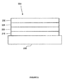
- FIG. 1 shows an organic light emitting device 100.
- Device 100 may include a substrate 110, an anode 115, a hole injection layer 120, a hole transport layer 125, an electron blocking layer 130, an emissive layer 135, a hole blocking layer 140, an electron transport layer 145, an electron injection layer 150, a protective layer 155, and a cathode 160.
- Cathode 160 is a compound cathode having a first conductive layer 162 and a second conductive layer 164.
- Device 100 may be fabricated by depositing the layers described, in order. The properties and functions of these various layers, as well as example materials, are described in more detail in US 7,279,704 at cols. 6-10.
- a flexible and transparent substrate-anode combination is disclosed in U.S. Pat. No. 5,844,363 .
- An example of a p-doped hole transport layer is m-MTDATA doped with F.sub.4-TCNQ at a molar ratio of 50:1, as disclosed in U.S. Patent Application Publication No. 2003/0230980 .
- Examples of emissive and host materials are disclosed in U.S. Pat. No. 6,303,238 to Thompson et al.
- An example of an n-doped electron transport layer is BPhen doped with Li at a molar ratio of 1:1, as disclosed in U.S. Patent Application Publication No. 2003/0230980 .
- U.S. Pat. Nos. 5,703,436 and 5,707,745 disclose examples of cathodes including compound cathodes having a thin layer of metal such as Mg:Ag with an overlying transparent, electrically-conductive, sputter-deposited ITO layer.
- the theory and use of blocking layers is described in more detail in U.S. Pat. No. 6,097,147 and U.S. Patent Application Publication No. 2003/0230980 .
- Examples of injection layers are provided in U.S. Patent Application Publication No. 2004/0174116 .
- a description of protective layers may be found in U.S. Patent Application Publication No. 2004/0174116 .
- FIG. 2 shows an inverted OLED 200.
- the device includes a substrate 210, a cathode 215, an emissive layer 220, a hole transport layer 225, and an anode 230.
- Device 200 may be fabricated by depositing the layers described, in order. Because the most common OLED configuration has a cathode disposed over the anode, and device 200 has cathode 215 disposed under anode 230, device 200 may be referred to as an "inverted" OLED. Materials similar to those described with respect to device 100 may be used in the corresponding layers of device 200.
- FIG. 2 provides one example of how some layers may be omitted from the structure of device 100.
- FIGS. 1 and 2 The simple layered structure illustrated in FIGS. 1 and 2 is provided by way of non-limiting example, and it is understood that embodiments of the invention may be used in connection with a wide variety of other structures.
- the specific materials and structures described are exemplary in nature, and other materials and structures may be used.
- Functional OLEDs may be achieved by combining the various layers described in different ways, or layers may be omitted entirely, based on design, performance, and cost factors. Other layers not specifically described may also be included. Materials other than those specifically described may be used. Although many of the examples provided herein describe various layers as comprising a single material, it is understood that combinations of materials, such as a mixture of host and dopant, or more generally a mixture, may be used. Also, the layers may have various sublayers.
- hole transport layer 225 transports holes and injects holes into emissive layer 220, and may be described as a hole transport layer or a hole injection layer.
- an OLED may be described as having an "organic layer" disposed between a cathode and an anode. This organic layer may comprise a single layer, or may further comprise multiple layers of different organic materials as described, for example, with respect to FIGS. 1 and 2 .
- OLEDs comprised of polymeric materials (PLEDs) such as disclosed in U.S. Pat. No. 5,247,190 to Friend et al.
- PLEDs polymeric materials
- OLEDs having a single organic layer may be used.
- OLEDs may be stacked, for example as described in U.S. Pat. No. 5,707,745 to Forrest et al.
- the OLED structure may deviate from the simple layered structure illustrated in FIGS. 1 and 2 .
- the substrate may include an angled reflective surface to improve out-coupling, such as a mesa structure as described in U.S. Pat. No. 6,091,195 to Forrest et al. , and/or a pit structure as described in U.S. Pat. No. 5,834,893 to Bulovic et al.
- any of the layers of the various embodiments may be deposited by any suitable method.
- preferred methods include thermal evaporation, ink-jet, such as described in U.S. Pat. Nos. 6,013,982 and 6,087,196 , organic vapor phase deposition (OVPD), such as described in U.S. Pat. No. 6,337,102 to Forrest et al ., and deposition by organic vapor jet printing (OVJP), such as described in U.S. patent application Ser. No. 10/233,470 .
- OVPD organic vapor phase deposition
- OJP organic vapor jet printing
- Other suitable deposition methods include spin coating and other solution based processes. Solution based processes are preferably carried out in nitrogen or an inert atmosphere.
- preferred methods include thermal evaporation.
- Preferred patterning methods include deposition through a mask, cold welding such as described in U.S. Pat. Nos. 6,294,398 and 6,468,819 , and patterning associated with some of the deposition methods such as ink-jet and OVJD. Other methods may also be used.
- the materials to be deposited may be modified to make them compatible with a particular deposition method.
- substituents such as alkyl and aryl groups, branched or unbranched, and preferably containing at least 3 carbons, may be used in small molecules to enhance their ability to undergo solution processing. Substituents having 20 carbons or more may be used, and 3-20 carbons is a preferred range. Materials with asymmetric structures may have better solution processibility than those having symmetric structures, because asymmetric materials may have a lower tendency to recrystallize. Dendrimer substituents may be used to enhance the ability of small molecules to undergo solution processing.
- Devices fabricated in accordance with embodiments of the invention may be incorporated into a wide variety of consumer products, including flat panel displays, computer monitors, televisions, billboards, lights for interior or exterior illumination and/or signaling, heads up displays, fully transparent displays, flexible displays, laser printers, telephones, cell phones, personal digital assistants (PDAs), laptop computers, digital cameras, camcorders, viewfinders, micro-displays, vehicles, a large area wall, theater or stadium screen, or a sign.
- PDAs personal digital assistants
- Various control mechanisms may be used to control devices fabricated in accordance with the present invention, including passive matrix and active matrix. Many of the devices are intended for use in a temperature range comfortable to humans, such as 18°C to 30°C., and more preferably at room temperature (20-25°C.).
- the materials and structures described herein may have applications in devices other than OLEDs.
- other optoelectronic devices such as organic solar cells and organic photodetectors may employ the materials and structures.
- organic devices such as organic transistors, may employ the materials and structures.
- halo, halogen, alkyl, cycloalkyl, alkenyl, alkynyl, arylkyl, heterocyclic group, aryl, aromatic group, and heteroaryl are known to the art, and are defined in US 7,279,704 at cols. 31-32.
- Novel compounds are provided, the compounds including 2-azatriphenylene (illustrated in FIG. 3 ).
- the compounds include 2-azatriphenylene having an additional aromatic substituent (i.e., aryl or heteroaryl). These compounds may be advantageously used in OLEDs to provide devices having improved stability and efficiency.
- One group of novel compounds include compounds having the formula of
- FORMULA I without a coordinated metal.
- these compounds are used as non-emitting compounds such as host materials and/or hole blocking layer materials.
- Another group of novel compounds are provided which include compounds wherein the 2-azatriphenylene structure is incorporated into a ligand coordinated to a metal (illustrated in FIG. 4 ). These compounds may be expected to demonstrate phosphorescent emissive properties because of the cyclometallated ligand. Thus, these compounds may be preferably used as emitting materials. In addition, these compounds may also be used as non-emitting materials in layers of a device which do not require the emissive properties of such compounds (e.g., hole blocking layer).
- Particular 2-azatriphenylene ligands include in a compound are provided.
- 1-azatriphenylene containing compounds have been reported in the literature ( see, JP2007189001 ). However, the class of compounds provided herein contain novel structures. The synthesis provided is directed to making 1-azatriphenylene compounds rather than a synthetic method for making 2-azatriphenylene compounds. Moreover, the 1-azatriphenylene synthetic methods are not necessarily applicable to making 2-azatriphenylene compounds.
- the methods provided herein are directed to 2-azatriphenylene compounds.
- 2-azatriphenylene compounds At least one example of 2-azatriphenylene compounds is reported in the literature ( see, Hewline, M. et al., Synthesis, 14: 2157-2163, 2007 ). However, the reference does not provide compounds having the additional aromatic substituent as provided herein and does not suggest 2-azatriphenylene compounds in the context of an OLED. 2-azatriphenylene compounds lacking the additional aromatic substituent may not be suitable for use in OLEDs.
- the additional aromatic group substituent at R 1 , R 2 , and/or R 3 on the 2-azatriphenylene core of the compound provides a novel structure and may also provide beneficial properties.
- the additional aromatic substituent i.e., an aryl or a heteroaryl
- the compounds provided herein may be particularly desirable.
- the beneficial properties of the compounds may apply to both emissive and non-emissive compounds.
- Triphenylene is a polyaromatic hydrocarbon with high triplet energy, yet high ⁇ -conjugation and a relatively small energy difference between the first singlet and first triplet levels. This would indicate that triphenylene has relatively easily accessible HOMO and LUMO levels compared to other aromatic compounds with similar triplet energy (e.g., biphenyl). Triphenylene and its derivatives may be especially good hosts at least because these compounds can accommodate red, green and even blue phosphorescent dopants to give high efficiency without energy quenching. High efficiency and high stability PHOLEDs with triphenylene hosts were demonstrated from previous work ( see , US2006/0280965 and PCT/US2008/072499 ).
- azatriphenylene has a lower LUMO than triphenylene (i.e., a LUMO more accessible than that of triphenylene) and thus azatriphenylene may improve electron transport in OLED devices.
- azatriphenylene may offer an improved charge balance that results in improvements in device performance in terms of lifetime, efficiency and low voltage.
- nitrogen in the 2 position of other host materials e.g., aza-dibenzothiophene
- nitrogen in the 2 position in azatriphenylene containing compounds i.e., 2-azatriphenylene
- nitrogen in the 2 position in azatriphenylene containing compounds i.e., 2-azatriphenylene
- the compounds provided may be particularly advantageous because the 2-azatriphenylene containing compounds may be more easily reduced than previously reported triphenylene compounds and derivatives.
- Table 1 provides the DFT calculation properties of triphenylene and its derivates.
- Table 1 contains the LUMO level as calculated for triphenylene, 1-azatriphenylene, and 2-azatriphenylene.
- the DFT calculation results shown in Table 1 demonstrate that 2-azatriphenylene has a LUMO of -1.34 eV notably lower than triphenylene and 1-azatriphenylene which have LUMO levels of -0.93 eV and -1.23 eV, respectively.
- Novel 2-azatriphenylene containing compounds are provided herein. These compounds provide a new type of materials which may be advantageously used in OLEDs. In particular, these compounds may be used in OLEDs fabricated by both vapor deposition or solution processing methods, thereby giving stable and efficient devices.
- Novel compounds are provided, the compounds include the structure:
- R 1 , R 2 , and R 3 may represent mono, di, tri, or tetra substitutions, and each of R 1 , R 2 , and R 3 are independently selected from the group consisting of hydrogen, alkyl, alkoxy, amino, alkenyl, alkynyl, arylkyl, aryl, and heteroaryl. At least one of R 1 , R 2 and R 3 is an aryl or a heteroaryl.
- R 1 is selected from the group consisting of alkyl, alkoxy, amino, alkenyl, alkynyl, arylkyl, aryl, and heteroaryl.
- R 1 is an aryl or heteroaryl.
- R 2 is selected from the group consisting of alkyl, alkoxy, amino, alkenyl, alkynyl, arylkyl, aryl, and heteroaryl.
- R 2 is an aryl or heteroaryl.
- R 3 is selected from the group consisting of alkyl, alkoxy, amino, alkenyl, alkynyl, arylkyl, aryl, and heteroaryl.
- R 3 is an aryl or heteroaryl.
- each of R 1 , R 2 , and R 3 is an aryl or a heteroaryl.
- One group of compounds provided include compounds having the formula:
- the compound is not coordinated to a metal.
- Such compounds may be further substituted at R 1 , R 2 and R 3 , as described above.
- These compounds may be used in a variety of layers, both emissive and non-emissive, within the device structure. Preferably, these compounds may be used as hosts in the emissive layer of an OLED. Such compounds may also be preferably used as non-emitting materials in other non-emissive layers of an OLED (e.g., hole blocking layer).
- R 3 is a substitution ortho to the nitrogen.
- R 3 substituent at the carbon next to the nitrogen i.e., ortho to the nitrogen
- the stability of the compound may be improved.
- the pyridine ring lacking substituents at the positions ortho to the nitrogen atom may be especially vulnerable to degradation and thus less stable.
- nitrogen bonds exposed in the absence of a substitution ortho to the nitrogen may be the weak link in possible degradation pathways.
- a substitution ortho to the nitrogen may provide steric protection to the pyridine ring thereby improving stability of the compound. Therefore, a compound having R 3 as an substitution ortho to the nitrogen may improve the stability of the 2-azatriphenylene compound.
- R' 3 , R 5 , R 6 , R 7 , and R 8 may represent mono, di, tri, tetra, or penta substitutions.
- R' 3 , R 4 , R 5 , R 6 , R 7 , and R 8 are independently selected from the group consisting of hydrogen, alkyl, alkoxy, amino, alkenyl, alkynyl, arylkyl, aryl, and heteroaryl.
- the compounds discussed above are not phosphorescent at room temperature. These compounds may be used as non-emitting materials in a device. Preferably, these compounds may be used as a host in the emissive layer of an OLED. More preferably, these compounds may be used as a host in the emissive layer of a phosphorescent OLED. These compounds may also be used as materials in a variety of other non-emissive layers within the device structure, such as a hole blocking material within a hole blocking layer.
- 2-azatriphenylene compounds which comprise a cyclometallated ligand. These compounds may be expected to have emissive properties as a result of the coordinated metal. Preferably, these compounds may be used as emitting materials within the emissive layer of OLEDs. These compounds may also be used an non-emitting materials in other layers of a device that do not require the emissive properties of the compounds. In particular, these compounds may be used as materials in a hole injection or transport layer.
- the compounds comprise a ligand L having the formula:
- the ligand L contains the 2-azatriphenylene structure, described in FORMULA I, with an aromatic substituent A positioned ortho to the nitrogen atom in the aza ring of the compound.
- R A is a 5-membered or 6-membered aryl or heteroaryl ring.
- R A may represent a mono, di, tri, or tetra substitution.
- R A is selected from the group consisting of hydrogen, alkyl, alkoxy, amino, alkenyl, alkynyl, arylkyl, aryl, and heteroaryl.
- the ligand L is coordinated to a metal having an atomic number greater than 40.
- the metal is Ir.
- homoleptic Ir complexes comprising 2-azatriphenylene are provided.
- compounds are provided wherein the ligand L is included in a homoleptic compound.
- heteroleptic Ir complexes are provided.
- compounds are provided wherein the ligand L is included in a heteroleptic compound.
- compounds having the formula (L) n (L') 3-n Ir are provided. n is 1 or 2. In one aspect, preferably n is 1. In another aspect, preferably n is 2. L' is selected from the group consisting of:
- R' 1 and R' 2 may represent mono, di, tri, or tetra substitutions.
- R' 1 and R' 2 are selected from the group consisting of hydrogen, alkyl, alkoxy, amino, alkenyl; alkynyl, arylkyl, aryl, and heteroaryl.
- L has a different structure than L' .
- R 4 and R 5 may represent mono, di, tri, or tetra substitutions.
- R 4 and R 5 are selected from the group consisting of hydrogen, alkyl, alkoxy, amino, alkenyl, alkynyl, arylkyl, aryl, and heteroaryl.
- ligand L is selected from the group consisting of:
- Particular compounds comprising an Ir complex containing a 2-azatriphenylene ligand are provided, including compounds selected from the group consisting of:
- R 4 , R 5 , R' 1, and R' 2 may represent, mono, di, tri, tetra, or substitutions.
- R 4 , R 5 , R' 1 , and R' 2 are independently selected from the group consisting of hydrogen, alkyl, alkoxy, amino, alkenyl, alkynyl, arylkyl, aryl, and heteroaryl.
- An organic light emitting device comprises an anode, a cathode, and a first organic emissive layer disposed between the anode and the cathode.
- the first organic emissive layer comprises a compound including the structure FORMULA I, as discussed above. Selections for the substituents described as preferred for the compounds including the structure FORMULA I are also preferred for use in a device that comprises a compound including the structure FORMULA I. These selections include those described for R 1 , R 2 , R 3 , and A.
- R 1 R 2 , and R 3 may represent mono, di, tri, or tetra substitution.
- R 1 , R 2 , and R 3 are independently selected from the group consisting of hydrogen, alkyl, alkoxy, amino, alkenyl, alkynyl, aryl, and heteroaryl. At least one of R 1 , R 2 , and R 3 is an aryl or heteroaryl.
- devices which contain a compound wherein R 1 is selected from the group consisting of alkyl, alkoxy, amino, alkenyl, alkynyl, aryl, and heteroaryl.
- R 1 is an aryl or a heteroaryl.
- devices are provided which contain a compound wherein R 2 is selected from the group consisting of alkyl, alkoxy, amino, alkenyl, alkynyl, aryl, and heteroaryl.
- R 2 is an aryl or a heteroaryl.
- devices which contain a compound wherein R 3 is selected from the group consisting of alkyl, alkoxy, amino, alkenyl, alkynyl, aryl, and heteroaryl.
- R 3 is an aryl or a heteroaryl.
- devices are provided which contain a compound wherein R 1 , R 2 , and R 3 are an aryl or a heteroaryl.
- Devices wherein the device includes a compound having the formula:
- the compound is not coordinated to a metal.
- Particular devices are provided, the device comprising a compound selected from the group consisting of Compound 1G - Compound 70G.
- R' 3 , R 4 , R 5 , R 6 , R7, and R 8 may represent mono, di, tri, tetra, or penta substitutions.
- R' 3 , R 4 , R 5 , R 6 , R 7 , and R 8 are independently selected from the group consisting of hydrogen, alkyl, alkoxy, amino, alkenyl, alkynyl, arylkyl, aryl and heteroaryl.
- Certain devices may contain a compound selected from the group consisting of Compound 1 - Compound 70 (i.e., R 1 , R 2 , R 3 , R 4 , R 5 , R 6 , R 7 , and R 8 are hydrogen).
- R 3 is a substitution ortho to the nitrogen.
- the first organic layer is an emissive layer and the compound including the structure FORMULA I is a host.
- the first organic layer of such a device may further comprise an emitting dopant.
- the first organic layer may comprise an emitting dopant having the formula:
- R x and R y may represent mono, di, tri, or tetra substitutions.
- R x and R y are independently selected from the group consisting of hydrogen, alkyl, and aryl.
- first organic layer is an emissive layer and the compound including the structure FORMULA II is an emitting dopant.
- the first organic layer of such a device may further comprise a host material.
- devices are also provided wherein the device comprises a second organic layer that is a non-emissive layer and the compound including the structure FORMULA II is a non-emissive material in the second organic layer.
- the second organic layer is a hole injection or transport layer and the compound including the structure FORMULA II is a hole injection or transport material.
- devices wherein the device includes a compound comprising a ligand L having the formula:
- R A is a 5-membered or 6-membered aryl or heteroaryl ring.
- R A may represent a mono, di, tri, or tetra substitution.
- R A is selected from the group consisting of hydrogen, alkyl, alkoxy, amino, alkenyl, alkynyl, arylkyl, aryl, and heteroaryl.
- the ligand L is coordinated to a metal having an atomic number greater than 40.
- the metal is Ir.
- ligand L is selected from the group consisting of:
- R 4 and R 5 may represent mono, di, tri, tetra, or penta substitutions.
- R 4 and R 5 are independently selected from hydrogen, alkyl, alkoxy, amino, alkenyl, alkynyl, aryl and heteroaryl.
- Devices containing a compound comprising a ligand selected from the group consisting of Compound 71 - Compound 78 are also provided.
- Devices containing a compound comprising an Ir complex containing a 2-azatriphenylene ligand are also provided, including devices containing a compound selected from the group consisting of Compound 79G - Compound 96G.
- Devices containing a specific compound are also provided, including devices containing a compound selected from the group consisting of Compound 79 - Compound 96.
- a consumer product comprising a device.
- the device further comprises an anode, a cathode, and a first organic layer disposed between the anode and the cathode.
- the first organic layer further comprises a compound that includes the structure FORMULA I, as described above. Selections for the substituents described as preferred for compounds having FORMULA I are also preferred for use in a device that includes a compound including the structure FORMULA I. These selections include those described for R 1 , R 2 , R 3 , R 4 , R 5 , R 6 , R 7 , R 8 , R' 1 , R' 2 , and A.
- R 1 , R 2 , and R 3 may represent mono, di, tri, or tetra substitution.
- R 1 , R 2 , and R 3 are independently selected from the group consisting of hydrogen, alkyl, alkoxy, amino, alkenyl, alkynyl, aryl, and heteroaryl. At least one of R 1 , R 2 , and R 3 is an aryl or heteroaryl.
- the materials described herein as useful for a particular layer in an organic light emitting device may be used in combination with a wide variety of other materials present in the device.
- emissive dopants disclosed herein may be used in conjunction with a wide variety of hosts, transport layers, blocking layers, injection layers, electrodes and other layers that may be present.
- the materials described or referred to below are non-limiting examples of materials that may be useful in combination with the compounds disclosed herein, and one of skill in the art can readily consult the literature to identify other materials that may be useful in combination.
- hole injection materials In addition to and / or in combination with the materials disclosed herein, many hole injection materials, hole transporting materials, host materials, dopant materials, exiton/hole blocking layer materials, electron transporting and electron injecting materials may be used in an OLED.
- Non-limiting examples of the materials that may be used in an OLED in combination with materials disclosed herein are listed in Table 2 below. Table 2 lists non-limiting classes of materials, non-limiting examples of compounds for each class, and references that disclose the materials. TABLE 2 MATERIAL EXAMPLES OF MATERIAL PUBLICATIONS Hole injection materials Phthalocyanine and porphryin compounds Appl. Phys. Lett. 69, 2160 (1996 ) Starburst triarylamines J. Lumin.
- Metal 8-hydroxyquinolates e.g., BAlq
- Electron transporting materials Anthracene-benzoimidazole compounds WO03060956
- Anthracene-benzothiazole compounds Appl. Phys. Lett.
- Step 1 Synthesis of 4-(biphenyl-2-yl)-2-metoxypyridine.
- Step 2 Synthesis of 3-methoxydibenzo[f,h]isoquinoline: 4-(biphenyl-2-yl)-2-methoxypyridine (2.9 g, 10.9 mmol), iodine (281 mg, 1.1 mmol) and toluene were charged into a double-walled quartz photochemical reactor equipped with magnetic stirring, an air bubbler and an ultraviolet lamp. Gentle air was bubbled through the solvent while it was irradiated for 15 h. The reaction mixture was purified by flash chromatography on silica (hexane: ethyl acetate) and sonicated in MeOH to give 3-methoxydibenzo[f,h]isoquinoline (0.5 g, 17%).
- Step 3 Synthesis of dibenzo[ f,h ]isoquinolin-3-ol.
- 3-methoxydibenzo[ f , h ]isoquinoline (1.0 g, 3.9 mmol) and pyridine hydrochloride (4.5 g, 39 mmol) were heated at ca. 220°C for 1.5 h.
- the reaction was cooled and water was added.
- the resulting solids were filtered, wash with water and dried in vacuum to give dibenzo[f,h]isoquinolin-3-ol (0.91 g, 95%).
- Step 4 Synthesis of dibenzo[ f,h ]isoquinolin-3-yl trifluoromethanesulfonate.
- Trifluoromethanesulfonic anhydride (5.2 g, 19 mmol) was added to a mixture of dibenzo[f,h]isoquinolin-3-ol (0.91 g, 3.7 mmol), pyridine (1.2 g, 15 mmol) and dichloromethane 100 mL under nitrogen at 0 °C and stirred overnight at room temperature. The reaction was quenched with saturated NaHCO 3 The organic layer was washed with water and dried on Na 2 SO4. The residue was purified by flash chromatography on silica (hexane: ethyl acetate) to give (1.1 g, 79%).
- Step 5 Synthesis of 4-(3-bromophenyl)dibenzo[ b,d ]thiophene.
- Step 6 Synthesis of 2-(3-(Dibenzo[ b,d ]thiophen-4-yl)phenyl)-4,4,5,5-tetramethyl-1,3,2-dioxaborolane.
- Step 7 Synthesis of 3-(3-(dibenzo[b,d]thiophen-4-yl)phenyl)dibenzo[f,h]isoquinoline.
- potassium phosphate tribasic monohydrate 2.0 g, 8.8 mmol
- 150 mL toluene and 15 mL water was prepared and bubbled with nitrogen for 20 minutes.
- All example devices were fabricated by high vacuum ( ⁇ 10 -7 Torr) thermal evaporation.
- the anode electrode is approximately 800 ⁇ or 1200 ⁇ of indium tin oxide (ITO).
- the cathode consisted of 10 ⁇ of LiF followed by 1000 ⁇ of A1. All devices are encapsulated with a glass lid sealed with an epoxy resin in a nitrogen glove box ( ⁇ 1ppm of H 2 O and O 2 ) immediately after fabrication, and a moisture getter was incorporated inside the package.
- an invention compound is the host material and the blocking layer material and E1 is the emitting dopant.
- the organic stack of Device Examples 1-4 consisted of sequentially, from the ITO surface, 100 ⁇ of E1 as the hole injecting layer (HIL), 300 ⁇ of 4,4'-bis-[N-(1-napthyl)-N-phenylamino]biphenyl ( ⁇ -NPD) as the hole transport layer (HTL), 300 ⁇ of Compound 1 doped with 10-15 % of E1, an Ir phosphorescent compound, as the emissive layer (EML), no blocking layer (0 ⁇ ) or 50 ⁇ of Compound 1 as the blocking layer (BL) and 450 ⁇ or 500 ⁇ of Alq 3 (tris-8-hydroxyquinoline aluminum) as the electron transport layer (ETL).
- HIL hole injecting layer
- ⁇ -NPD 4,4'-bis-[N-(1-napthyl)-N-phenylamino]biphenyl
- HTL hole
- Comparative Examples 1 and 2 were fabricated similarly to the Device Examples except that the CBP is used as the host and HPT was used as the BL material or there was no blocking layer.
- Table 3 shows the device structures and Table 4 shows the corresponding measured results for those devices.
- Comp. Ex. is an abbreviation for Comparative example.
- Ex. is an abbreviation for example.
- Cmpd. is an abbreviation for Compound.
- LE luminous efficiency, which is defined as the luminance divided by the driving current density of the OLED.
- EQE is external quantum efficiency, which is defined as the ratio of measured number of photons to the electrons passed across the junction.
- PE is power efficiency, which is defined as the total luminous flux emitted divided by the total power input.
- L 0 is the initial luminance, which is defined as the initial brightness at a certain current density.
- RT 80% is a measure of lifetime, which is defined as the time required for the initial luminance, L 0 , to decay to 80% of its value, at a constant current density of 40 mA/cm 2 at room temperature.
- Comparative Example 1 and Comparative Example 2 use thicknesses and dopant concentrations that were optimized for combinations of materials used in previous device studies.
- Device Example 1 and Device Example 2 have the same device structure and concentration of materials as used in Comparative Example 1 and Comparative Example 2, but the novel 2-azatriphenylene compounds provided herein have been substituted in place of CBP as the host material and HPT as the blocking layer material.
- Compound 1 as a host in green phosphorescent OLEDs gives high device efficiency (LE>40 cd/A at 1000 cd/m 2 ), indicating the azatriphenylenes linked with dibenzothiophenes, have triplet energy high enough for efficient green electrophosphorescence. This is consistent with the experimental results that the triplet energy of Compound 1 (T1 476 nm), which is high enough to accommodate a green phosphorescent dopant.
- Device Examples 1 and 2 were not optimized for lifetime analysis.
- the dopant concentration was adjusted as appropriate for these materials to measure device lifetime.
- the 2-azatriphenylene compounds significantly improve lifetime, as compared to Comparative Example 1 and Comparative Example 2 respectively.
- the Device Examples 3 and 4 improve lifetime while maintaining good efficiency.
- the high stability of devices incorporating Compound 1 as the host is notable in Device Example 3 and 4.
- the lifetime, T 80% (defined as the time required for the initial luminance, L 0 , to decay to 80% of its value, at a constant current density of 40 mA/cm 2 at room temperature) for Device Example 3 and Comparative 1 are 136 hours and 105 hours respectively, with Device Example 1 having a slightly higher L 0 .
- hosts containing azatriphenylenes are good host and enhancement layer materials for phosphorescent OLEDs, providing as least the similar efficiency and improvement in stability compared to the commonly used CBP as the host.
- More conjugated versions of triphenylene containing benzoselenophenes for example triphenylene and dibenzoselenophene units linked via p-phenylene (such as 4,4'-biphenyl) may be very suitable for lower energy (yellow to red) phosphorescent OLEDs.
Landscapes
- Chemical & Material Sciences (AREA)
- Organic Chemistry (AREA)
- Engineering & Computer Science (AREA)
- Materials Engineering (AREA)
- Physics & Mathematics (AREA)
- Spectroscopy & Molecular Physics (AREA)
- Inorganic Chemistry (AREA)
- Crystallography & Structural Chemistry (AREA)
- Manufacturing & Machinery (AREA)
- Optics & Photonics (AREA)
- Electroluminescent Light Sources (AREA)
- Other In-Based Heterocyclic Compounds (AREA)
- Plural Heterocyclic Compounds (AREA)
- Heterocyclic Carbon Compounds Containing A Hetero Ring Having Oxygen Or Sulfur (AREA)
Abstract
Description
- This application claims priority to
U.S. Provisional Application Serial No. 61/177,435, filed May 12, 2009 - The claimed invention was made by, on behalf of, and/or in connection with one or more of the following parties to a joint university corporation research agreement: Regents of the University of Michigan, Princeton University, The University of Southern California, and the Universal Display Corporation. The agreement was in effect on and before the date the claimed invention was made, and the claimed invention was made as a result of activities undertaken within the scope of the agreement.
- The present invention relates to novel organic materials that may be advantageously used in organic light emitting devices. More particularly, the present invention relates to novel 2-azatriphenylene containing compounds and devices containing such compounds.
- Opto-electronic devices that make use of organic materials are becoming increasingly desirable for a number of reasons. Many of the materials used to make such devices are relatively inexpensive, so organic opto-electronic devices have the potential for cost advantages over inorganic devices. In addition, the inherent properties of organic materials, such as their flexibility, may make them well suited for particular applications such as fabrication on a flexible substrate. Examples of organic opto-electronic devices include organic light emitting devices (OLEDs), organic phototransistors, organic photovoltaic cells, and organic photodetectors. For OLEDs, the organic materials may have performance advantages over conventional materials. For example, the wavelength at which an organic emissive layer emits light may generally be readily tuned with appropriate dopants.
- OLEDs make use of thin organic films that emit light when voltage is applied across the device. OLEDs are becoming an increasingly interesting technology for use in applications such as flat panel displays, illumination, and backlighting. Several OLED materials and configurations are described in
U.S. Pat. Nos. 5,844,363 ,6,303,238 , and5,707,745 , which are incorporated herein by reference in their entirety. - One application for phosphorescent emissive molecules is a full color display. Industry standards for such a display call for pixels adapted to emit particular colors, referred to as "saturated" colors. In particular, these standards call for saturated red, green, and blue pixels. Color may be measured using CIE coordinates, which are well known to the art.
- One example of a green emissive molecule is tris(2-phenylpyridine) iridium, denoted Ir(ppy)3, which has the structure:

- In this, and later figures herein, we depict the dative bond from nitrogen to metal (here, Ir) as a straight line.
- As used herein, the term "organic" includes polymeric materials as well as small molecule organic materials that may be used to fabricate organic opto-electronic devices. "Small molecule" refers to any organic material that is not a polymer, and "small molecules" may actually be quite large. Small molecules may include repeat units in some circumstances. For example, using a long chain alkyl group as a substituent does not remove a molecule from the "small molecule class. Small molecules may also be incorporated into polymers, for example as a pendent group on a polymer backbone or as a part of the backbone. Small molecules may also serve as the core moiety of a dendrimer, which consists of a series of chemical shells built on the core moiety. The core moiety of a dendrimer may be a fluorescent or phosphorescent small molecule emitter. A dendrimer may be a "small molecule, and it is believed that all dendrimers currently used in the field of OLEDs are small molecules.
- As used herein, "top" means furthest away from the substrate, while "bottom" means closest to the substrate. Where a first layer is described as "disposed over" a second layer, the first layer is disposed further away from substrate. There may be other layers between the first and second layer, unless it is specified that the first layer is "in contact with" the second layer. For example, a cathode may be described as "disposed over" an anode, even though there are various organic layers in between. As used herein, "solution processible" means capable of being dissolved, dispersed, or transported in and/or deposited from a liquid medium, either in solution or suspension form.
- A ligand may be referred to as "photoactive" when it is believed that the ligand directly contributes to the photoactive properties of an emissive material. A ligand may be referred to as "ancillary" when it is believed that the ligand does not contribute to the photoactive properties of an emissive material, although an ancillary ligand may alter the properties of a photoactive ligand.
- As used herein, and as would be generally understood by one skilled in the art, a first "Highest Occupied Molecular Orbital" (HOMO) or "Lowest Unoccupied Molecular Orbital" (LUMO) energy level is "greater than" or "higher than" a second HOMO or LUMO energy level if the first energy level is closer to the vacuum energy level. Since ionization potentials (IP) are measured as a negative energy relative to a vacuum level, a higher HOMO energy level corresponds to an IP having a smaller absolute value (an IP that is less negative). Similarly, a higher LUMO energy level corresponds to an electron affinity (EA) having a smaller absolute value (an EA that is less negative). On a conventional energy level diagram, with the vacuum level at the top, the LUMO energy level of a material is higher than the HOMO energy level of the same material. A "higher" HOMO or LUMO energy level appears closer to the top of such a diagram than a "lower" HOMO or LUMO energy level.
- As used herein, and as would be generally understood by one skilled in the art, a first work function is "greater than" or "higher than" a second work function if the first work function has a higher absolute value. Because work functions are generally measured as negative numbers relative to vacuum level, this means that a "higher" work function is more negative. On a conventional energy level diagram, with the vacuum level at the top, a "higher" work function is illustrated as further away from the vacuum level in the downward direction. Thus, the definitions of HOMO and LUMO energy levels follow a different convention than work functions.
- More details on OLEDs, and the definitions described above, can be found in
US Pat. No. 7,279,704 . - Novel organic compounds are provided. The compounds comprise 2-azatriphenylene containing compounds that may be advantageously used in OLEDs. In particular, these compounds may be used as a host material, hole blocking material, or ligand for an emissive metal complex. Devices containing a 2-azatriphenylene compounds provided herein may have improved stability and efficiency. Novel compounds are provided, the compounds including the structure:

- R1, R2, and R3 may represent mono, di, tri, or tetra substitutions. R1, R2, and R3 are independently selected from the group consisting of hydrogen, alkyl, alkoxy, amino, alkenyl, alkynyl, arylkyl, aryl, and heteroaryl. At least one of R1, R2, and R3 is an aryl or heteroaryl. Preferably, R3 is a substitution ortho to the nitrogen.
- One group of compounds are provided wherein the compound has the formula FORMULA I and the compound is not coordinated to a metal. Preferably, these compounds may be used as host materials in the emissive layer or as non-emitting materials in various other non-emissive layers in OLEDs.
- Preferably, R1 is selected from the group consisting of alkyl, alkoxy, amino, alkenyl, alkynyl, arylkyl, aryl, and heteroaryl. More preferably, R1 is an aryl or heteroaryl. Preferably, R2 is selected from the group consisting of alkyl, alkoxy, amino, alkenyl, alkynyl, arylkyl, aryl, and heteroaryl. More preferably, R2 is an aryl or heteroaryl. Preferably, R3 is selected from the group consisting of alkyl, alkoxy, amino, alkenyl, alkynyl, arylkyl, aryl, and heteroaryl. More preferably, R3 is an aryl or heteroaryl. Preferably, each of R1, R2, and R3 is an aryl or heteroaryl.
- Particular compounds having FORMULA I are provided including compounds selected from the group consisting of Compound 1G - Compound 70G. R'3, R5, R6, R7, and R8 may represent mono, di, tri, tetra, or penta substitutions. R'3, R5, R6 are independently selected from the group consisting of hydrogen, alkyl, alkoxy, amino, alkenyl, alkynyl, arylkyl, aryl, and heteroaryl. Specific compounds having FORMULA I are also provided. Each of R1, R2, R3, R4, R5, R6, R7, and R8 is hydrogen, such as compounds selected from the group consisting of Compound 1 - Compound 70.
- Another group of compounds containing a cyclometallated ligand are provided. The compounds comprise a ligand L having the formula:

- A is a 5-membered or 6-membered aryl or heteroaryl ring. RA may represent a mono, di, tri, or tetra substitution. RA is selected from the group consisting of hydrogen, alkyl, alkoxy, amino, alkenyl, alkynyl, arylkyl, aryl, and heteroaryl. The ligand L is coordinated to a metal having an atomic number greater than 40. Preferably, the metal is Ir.
- These compounds may be used as emitting materials because the cyclometallated complex of such compounds as ligands is expected to provide emissive properties. Preferably, these compounds may be used as emitting dopants in the emissive layer of an OLED. These compounds may also be used as non-emitting materials. In particular, the compounds may be used in parts of a device where the emissive properties of the compound are not used, such as the hole blocking layer.
- In one aspect, compounds are provided wherein the ligand L is included in a homoleptic compound. In another aspect, compounds are provided wherein the ligand L is included in a heteroleptic compound. In particular, compounds are provided wherein the compound has the formula (L)n(L')3-nIr. n is 1 or 2. In one aspect, preferably n is 1. In another aspect, preferably n is 2. L' is selected from the group consisting of:

- R'1 and R'2 may represent a mono, di, tri, or tetra substitutions. R'1 and R'2 is selected from the group consisting of hydrogen, alkyl, alkoxy, amino, alkenyl, alkynyl, arylkyl, aryl, and heteroaryl. L has a different structure than L'.
- Compounds comprising particular ligands are also provided, including compounds having a ligand L selected from the group consisting of Compound 71G - Compound 78G. R4 and R5 may represent mono, di, tri, tetra, or penta substitutions. R4 and R5 are independently selected from the group consisting of hydrogen, alkyl, alkoxy, amino, alkenyl, alkynyl, arylkyl, aryl, and heteroaryl. Specific ligands are also provided, including ligands L selected from the group consisting of Compound 71 - Compound 78 (i.e., R1, R2, R3, R4, and R5 are each hydrogen).
- Particular compounds comprising an Ir complex containing a 2-azatriphenylene ligand are also provided, including compounds selected from the group consisting of Compound 79G - Compound 96G. R4 and R5 are independently selected from the group consisting of hydrogen, alkyl, alkoxy, amino, alkenyl, alkynyl, arylkyl, aryl, and heteroaryl. Specific compounds comprising an Ir complex containing a 2-azatriphenylene ligand are also provided, including compounds selected from the group consisting of Compound 79 - Compound 96 (i.e., R1, R2, R3, R4, R5, R'1, and R'2 are each hydrogen).
- Additionally, an organic light emitting device is also provided. The device comprising an anode, a cathode, and a first organic layer, disposed between the anode and the cathode. The first organic layer further comprising a compound that includes the structure:

- R1, R2, and R3 may represent mono, di, tri, or tetra substitutions. R1, R2, and R3 are independently selected from the group consisting of hydrogen, alkyl, alkoxy, amino, alkenyl, alkynyl, arylkyl, aryl, and heteroaryl. At least one of R1, R2, and R3 is an aryl or heteroaryl.
- In one aspect, the device comprises a compound having the formula FORMULA I wherein the compound is not coordinated to a metal. Particular compounds that may be used in such devices include compounds selected from the group consisting of Compound 1G - Compound 70G. R'3, R4, R5, R6, R7, and R8 may represent mono, di, tri, tetra, or penta substitutions. R'3, R4, R5, R6, R7, and R8 are independently selected from the group consisting of hydrogen, alkyl, alkoxy, amino, alkenyl, alkynyl, arylkyl, aryl, and heteroaryl. Certain devices are provided which contain a compound selected from the group consisting of Compound 1 - Compound 70 (i.e., each of R1, R2, R3, R4, R5, R6, R7, and R8 is hydrogen).
- In another aspect, devices are provided wherein the first organic layer is an emissive layer and the compound including the structure FORMULA I is a host. Moreover, the first organic layer may further comprise an emitting dopant. Preferably, the emitting dopant has the formula:

- Additionally, devices are provided wherein the device comprises a compound comprising a ligand L having the formula:

- A is a 5-membered or 6-membered aryl or heteroaryl ring. RA may represent a mono, di, tri, or tetra substitution. RA is selected from the group consisting of hydrogen, alkyl, alkoxy, amino, alkenyl, alkynyl, arylkyl, aryl, and heteroaryl. Particular ligands for use in such devices include ligands L selected from the group consisting of Compound 71G - Compound 78G. R4 and R5 may represent mono, di, tri, tetra, or penta substitutions. R4 and R5 are independently selected from the group consisting of hydrogen, alkyl, alkoxy, amino, alkenyl, alkynyl, aryl, and heteroaryl. Certain devices are provided which contain a compound having a ligand L selected from the group consisting of Compound 71 - Compound 78 (i.e., R1, R2, R3, R4, and R5 are each hydrogen).
- Particular compounds for use in such devices include compounds selected from the group consisting of Compound 79G - Compound 96G. R4 and R5 may represent mono, di, tri, tetra, or penta substitutions. R4 and R5 are independently selected from the group consisting of hydrogen, alkyl, alkoxy, amino, alkenyl, alkynyl, aryl, and heteroaryl. Certain devices are provided which contain a compound selected from the group consisting of Compound 79 - Compound 96 (i.e., R1, R2, R3, R4, R5, R'1, and R'2 are each hydrogen).
- In one aspect, devices are provided wherein the first organic layer is an emissive layer and the compound including the structure FORMULA II is an emitting dopant. Preferably, the first organic layer further comprises a host material.
- In another aspect, devices are provided wherein the device comprises a second organic layer that is a non-emissive layer. The compound including the structure FORMULA II is a non-emissive material in the second organic layer. Preferably, the second organic layer is a hole injection or transport layer and the compound including the structure FORMULA II is a hole injection or transport material.
- Additionally, a consumer product comprising a device is also provided. The device further comprises an anode, a cathode, and a first organic layer disposed between the anode and the cathode. The first organic layer further comprises a compound including the structure FORMULA I, as described above. Selections for the substituents described as preferred for the compounds including the structure FORMULA I are also preferred for use in a device that comprises a compound including the structure FORMULA I. These selections include those described for R1, R2, R3, and A.
- R1, R2, and R3 may represent mono, di, tri, or tetra substitutions. R1, R2, and R3 are independently selected from the group consisting of alkyl, alkoxy, amino, alkenyl, alkynyl, arylkyl, aryl, heteroaryl and hydrogen. At least one of R1, R2, and R3 is an aryl or heteroaryl.
- In one aspect, the device of the consumer product may contain a 2-azatriphenylene compound having FORMULA II. In another aspect, the device of the consumer product may contain a compound comprising a ligand including 2-azatriphenylene coordinated to a metal having an atomic number greater than 40.
-
-
FIG. 1 shows an organic light emitting device. -
FIG. 2 shows an inverted organic light emitting device that does not have a separate electron transport layer. -
FIG. 3 shows a 2-azatriphenylene compound. -
FIG. 4 shows a ligand containing 2-azatriphenylene. - Generally, an OLED comprises at least one organic layer disposed between and electrically connected to an anode and a cathode. When a current is applied, the anode injects holes and the cathode injects electrons into the organic layer(s). The injected holes and electrons each migrate toward the oppositely charged electrode. When an electron and hole localize on the same molecule, an "exciton," which is a localized electron-hole pair having an excited energy state, is formed. Light is emitted when the exciton relaxes via a photoemissive mechanism. In some cases, the exciton may be localized on an excimer or an exciplex. Non-radiative mechanisms, such as thermal relaxation, may also occur, but are generally considered undesirable.
- The initial OLEDs used emissive molecules that emitted light from their singlet states ("fluorescence") as disclosed, for example, in
U.S. Pat. No. 4,769,292 . Fluorescent emission generally occurs in a time frame of less than 10 nanoseconds. - More recently, OLEDs having emissive materials that emit light from triplet states ("phosphorescence") have been demonstrated. Baldo et al., "Highly Efficient Phosphorescent Emission from Organic Electroluminescent Devices," Nature, vol. 395, 151-154, 1998; ("Baldo-I") and Baldo et al., "Very high-efficiency green organic light-emitting devices based on electrophosphorescence," Appl. Phys. Lett., vol. 75, No. 3, 4-6 (1999) ("Baldo-II"). Phosphorescence is described in more detail in
US Pat. No. 7,279,704 at cols. 5-6. -
FIG. 1 shows an organiclight emitting device 100. The figures are not necessarily drawn to scale.Device 100 may include asubstrate 110, ananode 115, ahole injection layer 120, ahole transport layer 125, anelectron blocking layer 130, anemissive layer 135, ahole blocking layer 140, anelectron transport layer 145, anelectron injection layer 150, aprotective layer 155, and acathode 160.Cathode 160 is a compound cathode having a firstconductive layer 162 and a secondconductive layer 164.Device 100 may be fabricated by depositing the layers described, in order. The properties and functions of these various layers, as well as example materials, are described in more detail inUS 7,279,704 at cols. 6-10. - More examples for each of these layers are available. For example, a flexible and transparent substrate-anode combination is disclosed in
U.S. Pat. No. 5,844,363 . An example of a p-doped hole transport layer is m-MTDATA doped with F.sub.4-TCNQ at a molar ratio of 50:1, as disclosed inU.S. Patent Application Publication No. 2003/0230980 . Examples of emissive and host materials are disclosed inU.S. Pat. No. 6,303,238 to Thompson et al. An example of an n-doped electron transport layer is BPhen doped with Li at a molar ratio of 1:1, as disclosed inU.S. Patent Application Publication No. 2003/0230980 .U.S. Pat. Nos. 5,703,436 and5,707,745 disclose examples of cathodes including compound cathodes having a thin layer of metal such as Mg:Ag with an overlying transparent, electrically-conductive, sputter-deposited ITO layer. The theory and use of blocking layers is described in more detail inU.S. Pat. No. 6,097,147 andU.S. Patent Application Publication No. 2003/0230980 . Examples of injection layers are provided inU.S. Patent Application Publication No. 2004/0174116 . A description of protective layers may be found inU.S. Patent Application Publication No. 2004/0174116 . -
FIG. 2 shows aninverted OLED 200. The device includes asubstrate 210, acathode 215, anemissive layer 220, ahole transport layer 225, and ananode 230.Device 200 may be fabricated by depositing the layers described, in order. Because the most common OLED configuration has a cathode disposed over the anode, anddevice 200 hascathode 215 disposed underanode 230,device 200 may be referred to as an "inverted" OLED. Materials similar to those described with respect todevice 100 may be used in the corresponding layers ofdevice 200.FIG. 2 provides one example of how some layers may be omitted from the structure ofdevice 100. - The simple layered structure illustrated in
FIGS. 1 and2 is provided by way of non-limiting example, and it is understood that embodiments of the invention may be used in connection with a wide variety of other structures. The specific materials and structures described are exemplary in nature, and other materials and structures may be used. Functional OLEDs may be achieved by combining the various layers described in different ways, or layers may be omitted entirely, based on design, performance, and cost factors. Other layers not specifically described may also be included. Materials other than those specifically described may be used. Although many of the examples provided herein describe various layers as comprising a single material, it is understood that combinations of materials, such as a mixture of host and dopant, or more generally a mixture, may be used. Also, the layers may have various sublayers. The names given to the various layers herein are not intended to be strictly limiting. For example, indevice 200,hole transport layer 225 transports holes and injects holes intoemissive layer 220, and may be described as a hole transport layer or a hole injection layer. In one embodiment, an OLED may be described as having an "organic layer" disposed between a cathode and an anode. This organic layer may comprise a single layer, or may further comprise multiple layers of different organic materials as described, for example, with respect toFIGS. 1 and2 . - Structures and materials not specifically described may also be used, such as OLEDs comprised of polymeric materials (PLEDs) such as disclosed in
U.S. Pat. No. 5,247,190 to Friend et al. By way of further example, OLEDs having a single organic layer may be used. OLEDs may be stacked, for example as described inU.S. Pat. No. 5,707,745 to Forrest et al. The OLED structure may deviate from the simple layered structure illustrated inFIGS. 1 and2 . For example, the substrate may include an angled reflective surface to improve out-coupling, such as a mesa structure as described inU.S. Pat. No. 6,091,195 to Forrest et al. , and/or a pit structure as described inU.S. Pat. No. 5,834,893 to Bulovic et al. - Unless otherwise specified, any of the layers of the various embodiments may be deposited by any suitable method. For the organic layers, preferred methods include thermal evaporation, ink-jet, such as described in
U.S. Pat. Nos. 6,013,982 and6,087,196 , organic vapor phase deposition (OVPD), such as described inU.S. Pat. No. 6,337,102 to Forrest et al ., and deposition by organic vapor jet printing (OVJP), such as described inU.S. patent application Ser. No. 10/233,470 . Other suitable deposition methods include spin coating and other solution based processes. Solution based processes are preferably carried out in nitrogen or an inert atmosphere. For the other layers, preferred methods include thermal evaporation. Preferred patterning methods include deposition through a mask, cold welding such as described inU.S. Pat. Nos. 6,294,398 and6,468,819 , and patterning associated with some of the deposition methods such as ink-jet and OVJD. Other methods may also be used. The materials to be deposited may be modified to make them compatible with a particular deposition method. For example, substituents such as alkyl and aryl groups, branched or unbranched, and preferably containing at least 3 carbons, may be used in small molecules to enhance their ability to undergo solution processing. Substituents having 20 carbons or more may be used, and 3-20 carbons is a preferred range. Materials with asymmetric structures may have better solution processibility than those having symmetric structures, because asymmetric materials may have a lower tendency to recrystallize. Dendrimer substituents may be used to enhance the ability of small molecules to undergo solution processing. - Devices fabricated in accordance with embodiments of the invention may be incorporated into a wide variety of consumer products, including flat panel displays, computer monitors, televisions, billboards, lights for interior or exterior illumination and/or signaling, heads up displays, fully transparent displays, flexible displays, laser printers, telephones, cell phones, personal digital assistants (PDAs), laptop computers, digital cameras, camcorders, viewfinders, micro-displays, vehicles, a large area wall, theater or stadium screen, or a sign. Various control mechanisms may be used to control devices fabricated in accordance with the present invention, including passive matrix and active matrix. Many of the devices are intended for use in a temperature range comfortable to humans, such as 18°C to 30°C., and more preferably at room temperature (20-25°C.).
- The materials and structures described herein may have applications in devices other than OLEDs. For example, other optoelectronic devices such as organic solar cells and organic photodetectors may employ the materials and structures. More generally, organic devices, such as organic transistors, may employ the materials and structures.
- The terms halo, halogen, alkyl, cycloalkyl, alkenyl, alkynyl, arylkyl, heterocyclic group, aryl, aromatic group, and heteroaryl are known to the art, and are defined in
US 7,279,704 at cols. 31-32. - Novel compounds are provided, the compounds including 2-azatriphenylene (illustrated in
FIG. 3 ). In particular, the compounds include 2-azatriphenylene having an additional aromatic substituent (i.e., aryl or heteroaryl). These compounds may be advantageously used in OLEDs to provide devices having improved stability and efficiency. - One group of novel compounds include compounds having the formula of
- FORMULA I without a coordinated metal. Preferably, these compounds are used as non-emitting compounds such as host materials and/or hole blocking layer materials. Another group of novel compounds are provided which include compounds wherein the 2-azatriphenylene structure is incorporated into a ligand coordinated to a metal (illustrated in
FIG. 4 ). These compounds may be expected to demonstrate phosphorescent emissive properties because of the cyclometallated ligand. Thus, these compounds may be preferably used as emitting materials. In addition, these compounds may also be used as non-emitting materials in layers of a device which do not require the emissive properties of such compounds (e.g., hole blocking layer). Particular 2-azatriphenylene ligands include in a compound are provided. - 1-azatriphenylene containing compounds have been reported in the literature (see,
JP2007189001 - The methods provided herein are directed to 2-azatriphenylene compounds.
- At least one example of 2-azatriphenylene compounds is reported in the literature (see, Hewline, M. et al., Synthesis, 14: 2157-2163, 2007). However, the reference does not provide compounds having the additional aromatic substituent as provided herein and does not suggest 2-azatriphenylene compounds in the context of an OLED. 2-azatriphenylene compounds lacking the additional aromatic substituent may not be suitable for use in OLEDs. The additional aromatic group substituent at R1, R2, and/or R3 on the 2-azatriphenylene core of the compound provides a novel structure and may also provide beneficial properties. In particular, the additional aromatic substituent (i.e., an aryl or a heteroaryl) may provide a further improvement in the stability of the compound via the additional conjugation. In addition, there are no known references providing synthetic methods for making 2-azatriphenylene compounds. Thus, for at least these reasons, the compounds provided herein may be particularly desirable. The beneficial properties of the compounds may apply to both emissive and non-emissive compounds.
- Moreover, most of the azatriphenylene compounds previously reported are 1-azatriphenylene compounds. While the synthesis of 1-azatriphenylenes is believed to be well known, the synthetic methods for making 1-azatriphenylenes do not necessarily apply to making 2-azatriphenylene compounds. Despite previous reports of azatriphenylene compounds, there have been no reports regarding the synthetic methods for making such 2-azatriphenylene compounds as provided herein. Many of the novel 2-azatriphenylene compounds provided can be synthesized using the methods described herein.
- Triphenylene is a polyaromatic hydrocarbon with high triplet energy, yet high π-conjugation and a relatively small energy difference between the first singlet and first triplet levels. This would indicate that triphenylene has relatively easily accessible HOMO and LUMO levels compared to other aromatic compounds with similar triplet energy (e.g., biphenyl). Triphenylene and its derivatives may be especially good hosts at least because these compounds can accommodate red, green and even blue phosphorescent dopants to give high efficiency without energy quenching. High efficiency and high stability PHOLEDs with triphenylene hosts were demonstrated from previous work (see,
US2006/0280965 andPCT/US2008/072499 ). - Compounds containing the triphenylene derivative azatriphenylene may be especially beneficial. Azatriphenylene has a lower LUMO than triphenylene (i.e., a LUMO more accessible than that of triphenylene) and thus azatriphenylene may improve electron transport in OLED devices. In addition, azatriphenylene may offer an improved charge balance that results in improvements in device performance in terms of lifetime, efficiency and low voltage. Moreover, previous work has shown that nitrogen in the 2 position of other host materials (e.g., aza-dibenzothiophene) may provide improvements. Without being limited to any theory as to how the invention works, it is thought that nitrogen in the 2 position in azatriphenylene containing compounds (i.e., 2-azatriphenylene) may also provide beneficial properties.
- In addition, the compounds provided may be particularly advantageous because the 2-azatriphenylene containing compounds may be more easily reduced than previously reported triphenylene compounds and derivatives. Table 1 provides the DFT calculation properties of triphenylene and its derivates. In particular, Table 1 contains the LUMO level as calculated for triphenylene, 1-azatriphenylene, and 2-azatriphenylene. The DFT calculation results shown in Table 1 demonstrate that 2-azatriphenylene has a LUMO of -1.34 eV notably lower than triphenylene and 1-azatriphenylene which have LUMO levels of -0.93 eV and -1.23 eV, respectively. Additionally, the DFT calculations shown in Table 1 suggest that the triplet energy of 2-azatriphenylene is similar to the triplet energy of triphenylene and 1-azatriphenylene, which was confirmed by the experimental results of Compound 1. Therefore, 2-azatriphenylene containing compounds may be more easily reduced and thus provide devices with low operating voltage.
TABLE 1 Compound HOMO (ev) LUMO (ev) Gap (ev) Dipole (debye) Calc. T1 (nm) 
-5.85 -0.93 -4.92 0.00 434 
-5.97 -1.23 -4.75 1.76 429 
-6.08 -1.43 -4.74 2.82 430 - Novel 2-azatriphenylene containing compounds are provided herein. These compounds provide a new type of materials which may be advantageously used in OLEDs. In particular, these compounds may be used in OLEDs fabricated by both vapor deposition or solution processing methods, thereby giving stable and efficient devices.
- Novel compounds are provided, the compounds include the structure:

- R1, R2, and R3 may represent mono, di, tri, or tetra substitutions, and each of R1, R2, and R3 are independently selected from the group consisting of hydrogen, alkyl, alkoxy, amino, alkenyl, alkynyl, arylkyl, aryl, and heteroaryl. At least one of R1, R2 and R3 is an aryl or a heteroaryl.
- In one aspect, R1 is selected from the group consisting of alkyl, alkoxy, amino, alkenyl, alkynyl, arylkyl, aryl, and heteroaryl. Preferably, R1 is an aryl or heteroaryl. In another aspect, R2 is selected from the group consisting of alkyl, alkoxy, amino, alkenyl, alkynyl, arylkyl, aryl, and heteroaryl. Preferably, R2 is an aryl or heteroaryl. In yet another aspect, R3 is selected from the group consisting of alkyl, alkoxy, amino, alkenyl, alkynyl, arylkyl, aryl, and heteroaryl. Preferably, R3 is an aryl or heteroaryl. In a further aspect, each of R1, R2, and R3 is an aryl or a heteroaryl.
- One group of compounds provided include compounds having the formula:

- The compound is not coordinated to a metal. Such compounds may be further substituted at R1, R2 and R3, as described above. These compounds may be used in a variety of layers, both emissive and non-emissive, within the device structure. Preferably, these compounds may be used as hosts in the emissive layer of an OLED. Such compounds may also be preferably used as non-emitting materials in other non-emissive layers of an OLED (e.g., hole blocking layer).
- Preferably, R3 is a substitution ortho to the nitrogen. By adding the R3 substituent at the carbon next to the nitrogen (i.e., ortho to the nitrogen), the stability of the compound may be improved. Without being bound by theory, it is thought that that the pyridine ring lacking substituents at the positions ortho to the nitrogen atom may be especially vulnerable to degradation and thus less stable. In particular, without being bound by theory, it is believed that nitrogen bonds exposed in the absence of a substitution ortho to the nitrogen may be the weak link in possible degradation pathways. Thus, a substitution ortho to the nitrogen may provide steric protection to the pyridine ring thereby improving stability of the compound. Therefore, a compound having R3 as an substitution ortho to the nitrogen may improve the stability of the 2-azatriphenylene compound.
- Particular compounds having the formula of FORMULA I are provided, wherein the compound is selected from the group consisting of:


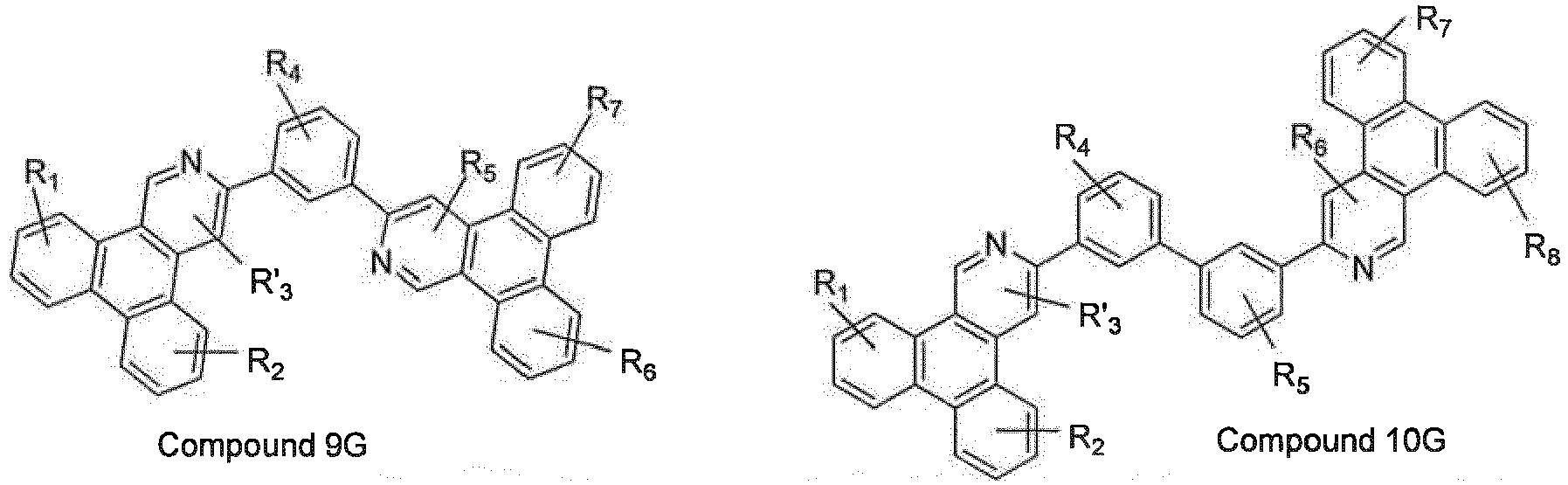


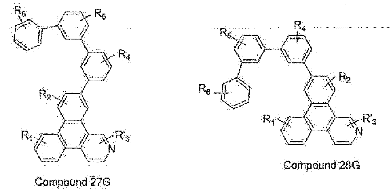


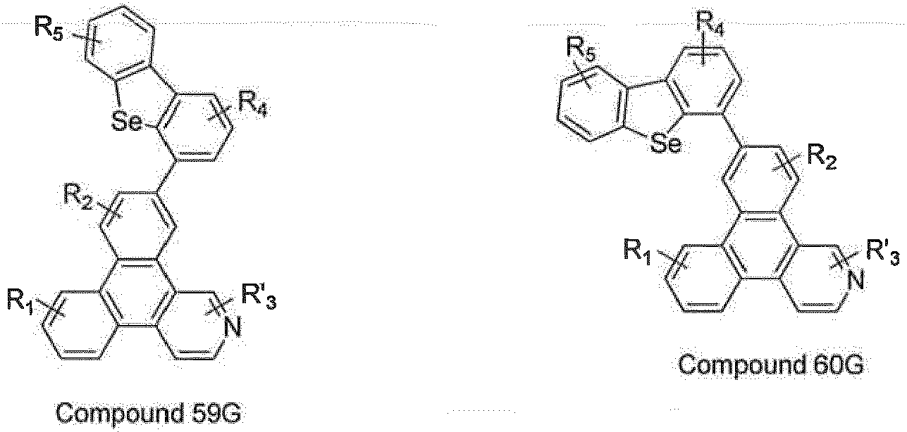

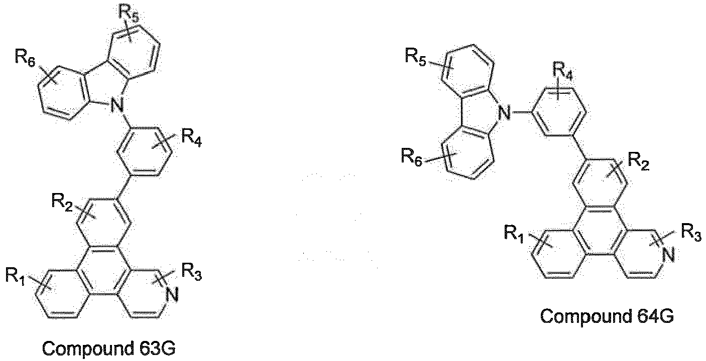


- R'3, R5, R6, R7, and R8 may represent mono, di, tri, tetra, or penta substitutions. R'3, R4, R5, R6, R7, and R8 are independently selected from the group consisting of hydrogen, alkyl, alkoxy, amino, alkenyl, alkynyl, arylkyl, aryl, and heteroaryl.
- In addition, specific examples of compounds having the formula of FORMULA I also are provided. Each of the substituents R1, R2, R3, R'3, R4, R5, R6, R7, and R8 is hydrogen. Specific compounds provided include compounds selected from the group consisting of:


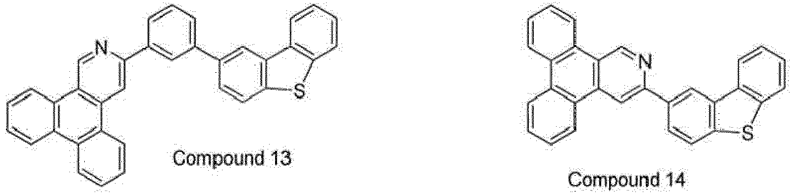


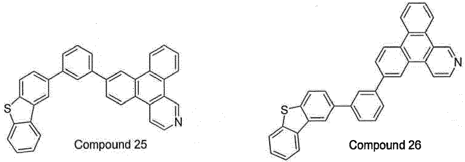


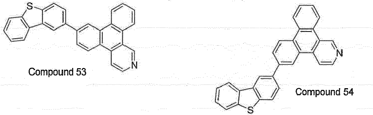


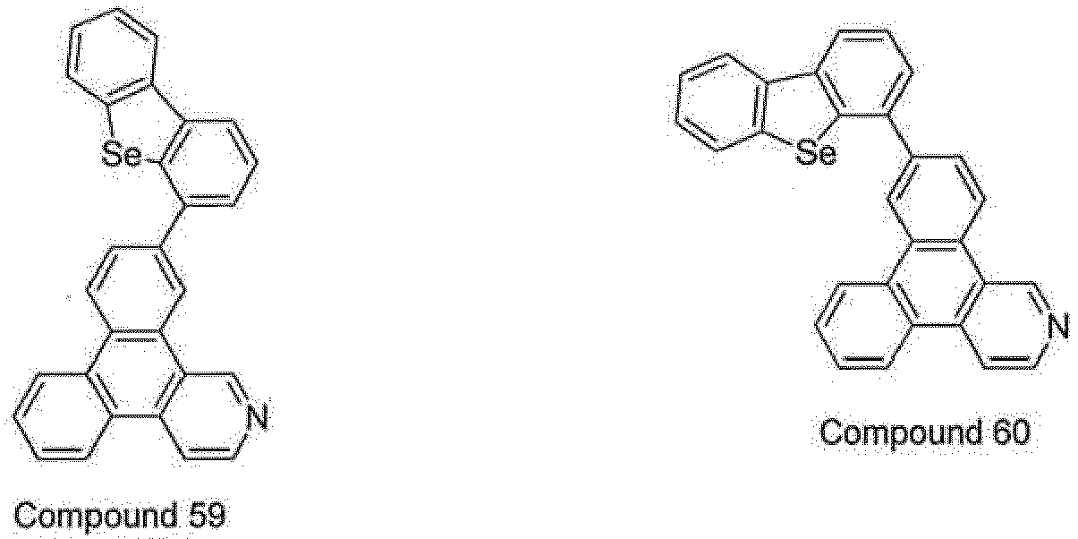


- The compounds discussed above (i.e, having the formula of FORMULA I without a coordinated metal) are not phosphorescent at room temperature. These compounds may be used as non-emitting materials in a device. Preferably, these compounds may be used as a host in the emissive layer of an OLED. More preferably, these compounds may be used as a host in the emissive layer of a phosphorescent OLED. These compounds may also be used as materials in a variety of other non-emissive layers within the device structure, such as a hole blocking material within a hole blocking layer.
- Another group of novel compounds provided herein are 2-azatriphenylene compounds which comprise a cyclometallated ligand. These compounds may be expected to have emissive properties as a result of the coordinated metal. Preferably, these compounds may be used as emitting materials within the emissive layer of OLEDs. These compounds may also be used an non-emitting materials in other layers of a device that do not require the emissive properties of the compounds. In particular, these compounds may be used as materials in a hole injection or transport layer.
- The compounds comprise a ligand L having the formula:

- The ligand L contains the 2-azatriphenylene structure, described in FORMULA I, with an aromatic substituent A positioned ortho to the nitrogen atom in the aza ring of the compound.
- A is a 5-membered or 6-membered aryl or heteroaryl ring. RA may represent a mono, di, tri, or tetra substitution. RA is selected from the group consisting of hydrogen, alkyl, alkoxy, amino, alkenyl, alkynyl, arylkyl, aryl, and heteroaryl. The ligand L is coordinated to a metal having an atomic number greater than 40. Preferably, the metal is Ir.
- In one aspect, homoleptic Ir complexes comprising 2-azatriphenylene are provided. In particular, compounds are provided wherein the ligand L is included in a homoleptic compound. In another aspect, heteroleptic Ir complexes are provided. In particular, compounds are provided wherein the ligand L is included in a heteroleptic compound. In yet another aspect, compounds having the formula (L)n(L')3-nIr are provided. n is 1 or 2. In one aspect, preferably n is 1. In another aspect, preferably n is 2. L' is selected from the group consisting of:
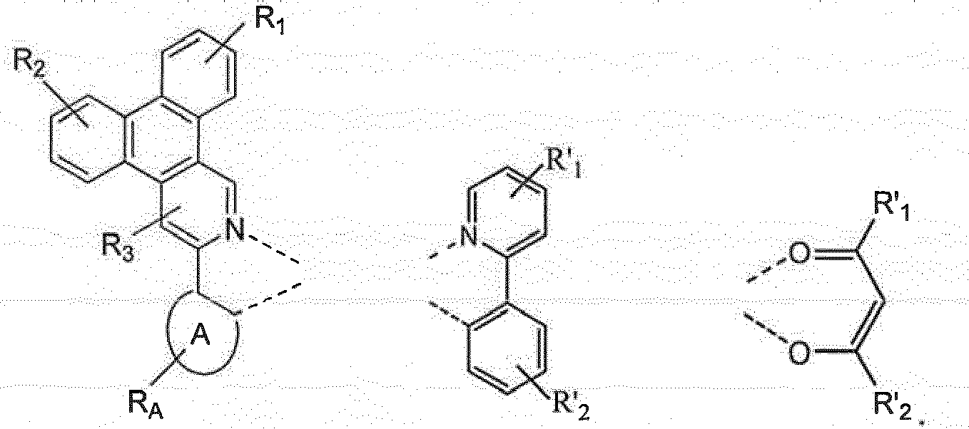
- R'1 and R'2 may represent mono, di, tri, or tetra substitutions. R'1 and R'2 are selected from the group consisting of hydrogen, alkyl, alkoxy, amino, alkenyl; alkynyl, arylkyl, aryl, and heteroaryl.
- L has a different structure than L' .
- Compounds including particular 2-azatriphenylene ligands are provided. The compound containing a ligand L selected from the group consisting of:


- R4 and R5 may represent mono, di, tri, or tetra substitutions. R4 and R5 are selected from the group consisting of hydrogen, alkyl, alkoxy, amino, alkenyl, alkynyl, arylkyl, aryl, and heteroaryl.
- In addition, compounds containing a specific 2-azatriphenylene ligand are provided. The ligand L is selected from the group consisting of:
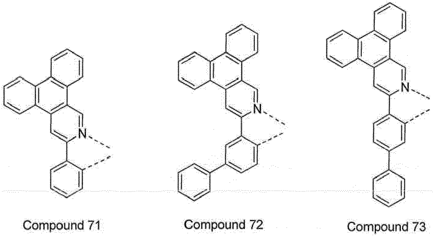


- Particular compounds comprising an Ir complex containing a 2-azatriphenylene ligand are provided, including compounds selected from the group consisting of:


- R4, R5, R'1, and R'2 may represent, mono, di, tri, tetra, or substitutions. R4, R5, R'1, and R'2 are independently selected from the group consisting of hydrogen, alkyl, alkoxy, amino, alkenyl, alkynyl, arylkyl, aryl, and heteroaryl.
- In addition, specific iridium complexes containing 2-azatriphenylene are also provided, including compounds selected from the group consisting of:


- An organic light emitting device is also provided. The device comprises an anode, a cathode, and a first organic emissive layer disposed between the anode and the cathode. The first organic emissive layer comprises a compound including the structure FORMULA I, as discussed above. Selections for the substituents described as preferred for the compounds including the structure FORMULA I are also preferred for use in a device that comprises a compound including the structure FORMULA I. These selections include those described for R1, R2, R3, and A.
- R1 R2, and R3 may represent mono, di, tri, or tetra substitution. R1, R2, and R3 are independently selected from the group consisting of hydrogen, alkyl, alkoxy, amino, alkenyl, alkynyl, aryl, and heteroaryl. At least one of R1, R2, and R3 is an aryl or heteroaryl.
- In one aspect, devices are provided which contain a compound wherein R1 is selected from the group consisting of alkyl, alkoxy, amino, alkenyl, alkynyl, aryl, and heteroaryl. Preferably, R1 is an aryl or a heteroaryl. In another aspect, devices are provided which contain a compound wherein R2 is selected from the group consisting of alkyl, alkoxy, amino, alkenyl, alkynyl, aryl, and heteroaryl. Preferably, R2 is an aryl or a heteroaryl. In yet another aspect, devices are provided which contain a compound wherein R3 is selected from the group consisting of alkyl, alkoxy, amino, alkenyl, alkynyl, aryl, and heteroaryl. Preferably, R3 is an aryl or a heteroaryl. In a further aspect, devices are provided which contain a compound wherein R1, R2, and R3 are an aryl or a heteroaryl.
- Devices are provided wherein the device includes a compound having the formula:

- The compound is not coordinated to a metal. Particular devices are provided, the device comprising a compound selected from the group consisting of Compound 1G - Compound 70G. R'3, R4, R5, R6, R7, and R8 may represent mono, di, tri, tetra, or penta substitutions. R'3, R4, R5, R6, R7, and R8 are independently selected from the group consisting of hydrogen, alkyl, alkoxy, amino, alkenyl, alkynyl, arylkyl, aryl and heteroaryl. Certain devices are provided which may contain a compound selected from the group consisting of Compound 1 - Compound 70 (i.e., R1, R2, R3, R4, R5, R6, R7, and R8 are hydrogen).
- Preferably, R3 is a substitution ortho to the nitrogen.
- Additionally, devices are provided wherein the first organic layer is an emissive layer and the compound including the structure FORMULA I is a host. Moreover, the first organic layer of such a device may further comprise an emitting dopant. In particular, the first organic layer may comprise an emitting dopant having the formula:

- Rx and Ry may represent mono, di, tri, or tetra substitutions. Rx and Ry are independently selected from the group consisting of hydrogen, alkyl, and aryl.
- Additionally, devices are also provided wherein the first organic layer is an emissive layer and the compound including the structure FORMULA II is an emitting dopant. Moreover, the first organic layer of such a device may further comprise a host material.
- Moreover, devices are also provided wherein the device comprises a second organic layer that is a non-emissive layer and the compound including the structure FORMULA II is a non-emissive material in the second organic layer. Preferably, the second organic layer is a hole injection or transport layer and the compound including the structure FORMULA II is a hole injection or transport material.
- In another aspect, devices are provided wherein the device includes a compound comprising a ligand L having the formula:

- A is a 5-membered or 6-membered aryl or heteroaryl ring. RA may represent a mono, di, tri, or tetra substitution. RA is selected from the group consisting of hydrogen, alkyl, alkoxy, amino, alkenyl, alkynyl, arylkyl, aryl, and heteroaryl. The ligand L is coordinated to a metal having an atomic number greater than 40. Preferably, the metal is Ir.
- Particular devices are provided wherein the ligand L is selected from the group consisting of:


- R4 and R5 may represent mono, di, tri, tetra, or penta substitutions. R4 and R5 are independently selected from hydrogen, alkyl, alkoxy, amino, alkenyl, alkynyl, aryl and heteroaryl.
- Devices containing a compound comprising a ligand selected from the group consisting of Compound 71 - Compound 78 are also provided.
- Devices containing a compound comprising an Ir complex containing a 2-azatriphenylene ligand are also provided, including devices containing a compound selected from the group consisting of Compound 79G - Compound 96G. Devices containing a specific compound are also provided, including devices containing a compound selected from the group consisting of Compound 79 - Compound 96.
- Additionally, a consumer product comprising a device is also provided. The device further comprises an anode, a cathode, and a first organic layer disposed between the anode and the cathode. The first organic layer further comprises a compound that includes the structure FORMULA I, as described above. Selections for the substituents described as preferred for compounds having FORMULA I are also preferred for use in a device that includes a compound including the structure FORMULA I. These selections include those described for R1, R2, R3, R4, R5, R6, R7, R8, R'1, R'2, and A.
- R1, R2, and R3 may represent mono, di, tri, or tetra substitution. R1, R2, and R3 are independently selected from the group consisting of hydrogen, alkyl, alkoxy, amino, alkenyl, alkynyl, aryl, and heteroaryl. At least one of R1, R2, and R3 is an aryl or heteroaryl.
- The materials described herein as useful for a particular layer in an organic light emitting device may be used in combination with a wide variety of other materials present in the device. For example, emissive dopants disclosed herein may be used in conjunction with a wide variety of hosts, transport layers, blocking layers, injection layers, electrodes and other layers that may be present. The materials described or referred to below are non-limiting examples of materials that may be useful in combination with the compounds disclosed herein, and one of skill in the art can readily consult the literature to identify other materials that may be useful in combination.
- In addition to and / or in combination with the materials disclosed herein, many hole injection materials, hole transporting materials, host materials, dopant materials, exiton/hole blocking layer materials, electron transporting and electron injecting materials may be used in an OLED. Non-limiting examples of the materials that may be used in an OLED in combination with materials disclosed herein are listed in Table 2 below. Table 2 lists non-limiting classes of materials, non-limiting examples of compounds for each class, and references that disclose the materials.
TABLE 2 MATERIAL EXAMPLES OF MATERIAL PUBLICATIONS Hole injection materials Phthalocyanine and porphryin compounds 
Appl. Phys. Lett. 69, 2160 (1996) Starburst triarylamines 
J. Lumin. 72-74, 985 (1997) CFx Fluorohydrocarbon polymer 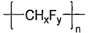
Appl. Phys. Lett. 78, 673 (2001) Conducting polymers (e.g., PEDOT:PSS, polyaniline, polypthiophene) 
Synth. Met. 87, 171 (1997) Arylamines complexed with metal oxides such as molybdenum and tungsten oxides 
SID Symposium Digest, 37, 923 (2006) Hole transporting materials Triarylamines (e.g., TPD, α-NPD) 
Appl. Phys. Lett. 51, 913 (1987) 
US5061569 
EP650955 
J. Mater. Chem. 3, 319 (1993) 
Appl. Phys. Lett. 90, 183503 (2007) 
Appl. Phys. Lett. 90, 183503 (2007) Triaylamine on spirofluorene core 
Synth. Met. 91, 209 (1997) Arylamine carbazole compounds 
Adv. Mater. 6, 677 (1994) Indolocarbazoles 
Synth. Met. 111,421 (2000) Isoindole compounds 
Chem. Mater. 15, 3148 (2003) Phosphorescent OLED host materials Red hosts Arylcarbazoles 
Appl. Phys. Lett. 78, 1622(2001) Metal 8-hydroxyquinolates (e.g., Alq3, BAlq) 
Nature 395, 151 (1998) 
US20060202194 
WO2005014551 Metal phenoxybenzothiazole compounds 
Appl. Phys. Lett. 90, 123509(2007) Conjugated oligomers and polymers (e.g., polyfluorene) 
Org. Electron. 1,15 (2000) Green hosts Arylcarbazoles 
Appl. Phys. Lett. 78, 1622 (2001) 
US2003175553 
WO2001039234 Aryltriphenylene compounds 
US20060280965 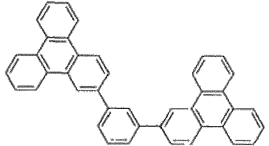
US20060280965 Polymers (e.g., PVK) 
Appl. Phys. Lett. 77, 2280 (2000) Spirofluorene compounds 
WO2004093207 Metal phenoxybenzooxazole compounds 
WO050890 
WO06132173 
JP200511610 Spirofluorene-carbazole compounds 
JP2007254297 
JP2007254297 Indolocabazoles 
WO07063796 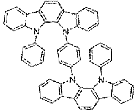
WO07063754 5-member ring electron deficient heterocycles (e.g., triazole, oxadiazole) 
J. Appl. Phys. 90, 5048 (2001) 
WO04107822 Metal phenoxypyridine compounds 
WO05030900 Blue hosts Arylcarbazoles 
Appl. Phys. Lett, 82, 2422 (2003) 
US20070190359 Dibenzothiophene-carbazole compounds 
WO2006114966 Phosphorescent dopants Red dopants Heavy metal porphyrins (e.g., PtOEP) 
Nature 395, 151 (1998) Iridium(III) organometallic complexes 
Appl. Phys. Lett. 78, 1622 (2001) 
US06835469 
US06835469 
US20060202194 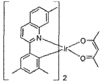
US20060202194 
US07087321 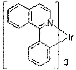
US07087321 
Adv. Mater.19,739 (2007) Platinum(II) organometallic complexes 
WO2003040257 Osminum(III) complexes 
Chem.Mater.17.3532 (2005) Ruthenium(II) complexes 
Adv. Mater. 17, 1059 (2005) Green dopants Iridium(III) organometallic complexes 
Inorg.Chem.40, 1704 (2001) 
US2002034656 
US06687266 
Chem. Mater. 16,2480 (2004) 
US2007190359 
US 2006008670 JP2007123392 
Adv. Mater. 16, 2003 (2004) 
Angew. Chem. Int. Ed. 2006,45,7800 Pt(II) organometallic complexes 
Appl. Phys. Lett. 86, 153505 (2005) 
Appl. Phys. Lett. 86, 153505 (2005) 
Chem. Lett. 34, 592 (2005) Gold complexes 
Chem. Commun. 2906 (2005) Rhenium(III) complexes 
Inorg. Chem. 42, 1248 (2003) Blue dopants Iridium(III) organometallic complexes 
WO2002002714 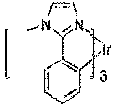
WO2006009024 
US2006251923 
WO2006056418 ,US2005260441 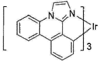
US2007190359 
US2002134984 
Angew. Chem. Int. Ed. 47, 1 (2008) 
Chem. Mater. 18, 5119 (2006) 
Inorg. Chem. 46, 4308 (2007) 
WO05123873 
WO05123873 
WO07004380 
WO06082742 Osmium(II) complexes 
US2005260449 
Organometallics 23, 3745 (2004) Gold complexes 
Appl. Phys. Lett.74,1361 (1999) Platinum(II) complexes 
WO06098120 WO06103874 Exciton/hole blocking layer materials Bathocuprine compounds (e.g., BCP, BPhen) 
Appl. Phys. Lett. 75, 4 (1999) 
Appl. Phys. Lett. 79, 449 (2001) Metal 8-hydroxyquinolates (e.g., BAlq) 
Appl. Phys. Lett. 81, 162(2002) 5-member ring electron deficient heterocycles such as triazole, oxadiozole, imidazole, benzoimidazole 
Appl. Phys. Lett. 81, 162(2002) Triphenylene compounds 
US20050025993 Fluorinated aromatic compounds 
Appl. Phys. Lett. 79, 156(2001) Electron transporting materials Anthracene-benzoimidazole compounds 
WO03060956 Anthracene-benzothiazole compounds 
Appl. Phys. Lett. 89, 063504 (2006) Metal 8-hydroxyquinolates (e.g., Alq3) 
Appl. Phys. Lett. 51, 913 (1987) Metal hydroxybenoquinolates 
Chem. Lett. 5, 905 (1993) Bathocuprine compounds such as BCP, BPhen, etc 
Appl. Phys. Lett. 91, 263503(2007) 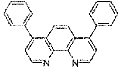
Appl. Phys. Lett. 79, 449 (2001) 5-member ring electron deficient heterocycles (e.g.,triazole, oxadiazole, imidazole, benzoimidazole) 
Appl. Phys. Lett. 74, 865 (1999) 
Appl. Phys. Lett. 55, 1489 (1989) 
Jpn. J. Apply. Phys. 32, L917 (1993) Silole compounds 
Org. Electron. 4, 113 (2003) Arylborane compounds 
J. Am. Chem. Soc. 120, 9714 (1998) Fluorinated aromatic compounds 
J. Am. Chem. Soc. 122, 1832 (2000) -

- Step 1. Synthesis of 4-(biphenyl-2-yl)-2-metoxypyridine. A nitrogen flushed mixture of 4-chloro-2-methoxypyridine (3.0 g, 21.03 mmol), 2-biphenylboronic acid 5.0 g, 25.23 mmol), Pd2(dba)3 (381 mg, 0.414 mmol), 2-dicyclohexylphosphino-2',6'-dimethoxybiphenyl (681 mg, 1.66 mmol), toluene (250 mL) and a slurry of K3PO4H2O (14.57 g, 63.09 mmol) in water (25 mL) were refluxed for 18 h. After the mixture cooled to room temperature the organic layer was dried over anhydrous Na2SO4, filtered, and concentrated in vacuum. The residue was purified by flash chromatography on silica (hexane: ethyl acetate) and recrystallized from ethyl acetate to give 4-(biphenyl-2-yl)-2-methoxypyridine (4.2 g, 76.5%).

- Step 2. Synthesis of 3-methoxydibenzo[f,h]isoquinoline: 4-(biphenyl-2-yl)-2-methoxypyridine (2.9 g, 10.9 mmol), iodine (281 mg, 1.1 mmol) and toluene were charged into a double-walled quartz photochemical reactor equipped with magnetic stirring, an air bubbler and an ultraviolet lamp. Gentle air was bubbled through the solvent while it was irradiated for 15 h. The reaction mixture was purified by flash chromatography on silica (hexane: ethyl acetate) and sonicated in MeOH to give 3-methoxydibenzo[f,h]isoquinoline (0.5 g, 17%).
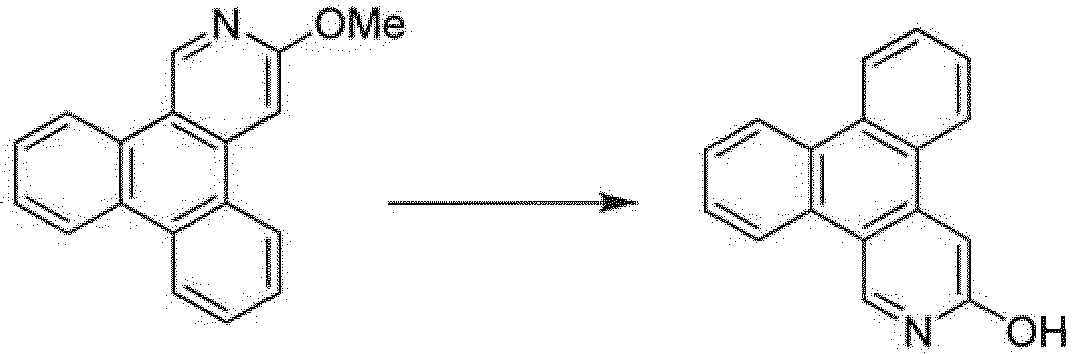
- Step 3. Synthesis of dibenzo[f,h]isoquinolin-3-ol. 3-methoxydibenzo[f,h]isoquinoline (1.0 g, 3.9 mmol) and pyridine hydrochloride (4.5 g, 39 mmol) were heated at ca. 220°C for 1.5 h. The reaction was cooled and water was added. The resulting solids were filtered, wash with water and dried in vacuum to give dibenzo[f,h]isoquinolin-3-ol (0.91 g, 95%).

- Step 4. Synthesis of dibenzo[f,h]isoquinolin-3-yl trifluoromethanesulfonate. Trifluoromethanesulfonic anhydride (5.2 g, 19 mmol) was added to a mixture of dibenzo[f,h]isoquinolin-3-ol (0.91 g, 3.7 mmol), pyridine (1.2 g, 15 mmol) and
dichloromethane 100 mL under nitrogen at 0 °C and stirred overnight at room temperature. The reaction was quenched with saturated NaHCO3 The organic layer was washed with water and dried on Na2SO4. The residue was purified by flash chromatography on silica (hexane: ethyl acetate) to give (1.1 g, 79%).
- Step 5. Synthesis of 4-(3-bromophenyl)dibenzo[b,d]thiophene. A nitrogen flushed mixture of 1, 3-dibromobenzene (18.63 g, 78.92 mmol), dibenzo{b,d}thiophen-4-ylboronic acid (6.0 g, 26.3 mmol), Pd(PPh3)4 (304 mg, 0.414 mmol), toluene (200 mL) and a slurry of K2CO3 (10.9 g, 78.92 mmol) in water (20 mL) were refluxed for 23 h. After the mixture cooled to room temperature the organic layer was washed with water, dried over anhydrous Na2SO4, filtered, and concentrated in vacuo. The residue was purified by vacuum distillation (Kugelrohr) followed by flash chromatography on silica (hexane: dichloromethane) to give 4-(3-bromophenyl)dibenzo[b,d]thiophene (3.5 g 39.2 %).

- Step 6. Synthesis of 2-(3-(Dibenzo[b,d]thiophen-4-yl)phenyl)-4,4,5,5-tetramethyl-1,3,2-dioxaborolane. A nitrogen flushed mixture of 4-(3-bromophenyl)dibenzo[b,d]thiophene (2.4 g 7.07 mmol), 4,4,4',4',5,5,5',5'-octamethyl-2,2'-bi(1,3,2-dioxaborolane (3.58 g, 14 mmol), Pd(dppf)Cl2 (114 mg, 0.14 mmol) and KOAc (2.08g, 21.2 mmol) was heated in dioxane (100 mL) at 90°C for 18 h. After the mixture cooled to room temperature, ethyl acetate was added and the organic layer was washed with water, washed with brine, dried over anhydrous Na2SO4 and filtered. Celite was added to the filtrate and then concentrated by vacuum. The residue was purified by flash chromatography on silica (hexane: dichloromethane) followed by vacuum distillation (Kugelrohr) to remove the excess 4,4,4',4',5,5,5',5'-octamethyl-2,2'-bi(1,3,2-dioxaborolane and then crystallized from hexanes: ethyl acetate to give 2-(3-(dibenzo[b,d]thiophen-4-yl)phenyl)-4,4,5,5-tetramethyl-1,3,2-dioxaborolane (1.62 g, 59%).

- Step 7. Synthesis of 3-(3-(dibenzo[b,d]thiophen-4-yl)phenyl)dibenzo[f,h]isoquinoline. The mixture of Step 4 product dibenzo[f,h]isoquinolin-3-yl trifluoromethanesulfonate (1.1g, 2.9 mmol), Step 6 product 2-(3-(dibenzo[b,d]thiophen-4-yl)phenyl)-4,4,5,5-tetramethyl-1,3,2-dioxaborolane (1.5 g, 3.8 mmol), potassium phosphate tribasic monohydrate (2.0 g, 8.8 mmol), 150 mL toluene and 15 mL water was prepared and bubbled with nitrogen for 20 minutes. Then tris(dibenzylideneacetone)dipalladium(0) (27 mg, 0.029 mmol) and 2-dicyclohexylphosphino-2',6'-dimethoxybiphenyl (48 mg, 0.12 mmol) were added to the mixture. The reaction mixture was bubbled with nitrogen for another 20 minutes and then refluxed overnight. After cooled to room temperature, 2-(3-(dibenzo[b,d]thiophen-4-yl)phenyl)-4,4,5,5-tetramethyl-1,3,2-dioxaborolane (1.3 g, 3.4 mmol), tris(dibenzylideneacetone)dipalladium(0) (60 mg, 0.066 mmol) and 2-dicyclohexylphosphino-2',6'-dimethoxybiphenyl (100 mg, 0.24 mmol) were added to the mixture. The reaction mixture was bubbled with nitrogen for 30 minutes and then refluxed overnight. The mixture then was cooled to room temperature. The organic layer was collected and dried by MgSO4. The crude product was purified by silica gel column to give white solid Compound 1 (1.0 g, 71% yield).
- Synthesis of ligand 3-phenyldibenzo[f,h]isoquinoline. Dibenzo[f,h]isoquinolin-3-yl trifluoromethanesulfonate compound as synthesized in above Step 4 of Compound 1 synthesis reacts with phenylboronic acid under Suzuki reaction condition as described in Step 7 of Compound 1 synthesis to give the ligand 3-phenyldibenzo [f,h] isoquinoline.

- Synthesis of Iridium complex Compound 79. 3-Phenyldibenzo[f,h]isoquinoline ligand mixed with Ir(acac)3 in ethylene glycol are heated up to reflux under nitrogen overnight to give Compound 79. The molar ratio of ligand and Ir(acac)3 is about 3.5 to 1.
- All example devices were fabricated by high vacuum (<10-7 Torr) thermal evaporation. The anode electrode is approximately 800 Å or 1200 Å of indium tin oxide (ITO). The cathode consisted of 10 Å of LiF followed by 1000 Å of A1. All devices are encapsulated with a glass lid sealed with an epoxy resin in a nitrogen glove box (<1ppm of H2O and O2) immediately after fabrication, and a moisture getter was incorporated inside the package.
- Particular devices are provided wherein an invention compound, Compound 1, is the host material and the blocking layer material and E1 is the emitting dopant. The organic stack of Device Examples 1-4 consisted of sequentially, from the ITO surface, 100 Å of E1 as the hole injecting layer (HIL), 300 Å of 4,4'-bis-[N-(1-napthyl)-N-phenylamino]biphenyl (α-NPD) as the hole transport layer (HTL), 300 Å of Compound 1 doped with 10-15 % of E1, an Ir phosphorescent compound, as the emissive layer (EML), no blocking layer (0 Å) or 50 Å of Compound 1 as the blocking layer (BL) and 450 Å or 500 Å of Alq3 (tris-8-hydroxyquinoline aluminum) as the electron transport layer (ETL).
- Comparative Examples 1 and 2 were fabricated similarly to the Device Examples except that the CBP is used as the host and HPT was used as the BL material or there was no blocking layer.
- As used herein, the following compounds have the following structures:


- The device structures and device data are summarized below in Table 3 and Table 4.
- Table 3 shows the device structures and Table 4 shows the corresponding measured results for those devices.
- The following terms are used in Tables 3 and 4, and are defined herein:
Comp. Ex. is an abbreviation for Comparative example. Ex. is an abbreviation for example. Cmpd. is an abbreviation for Compound. LE is luminous efficiency, which is defined as the luminance divided by the driving current density of the OLED. EQE is external quantum efficiency, which is defined as the ratio of measured number of photons to the electrons passed across the junction. PE is power efficiency, which is defined as the total luminous flux emitted divided by the total power input. L0 is the initial luminance, which is defined as the initial brightness at a certain current density. RT80% is a measure of lifetime, which is defined as the time required for the initial luminance, L0, to decay to 80% of its value, at a constant current density of 40 mA/cm2 at room temperature.TABLE 3 Device Example Host Dopant % BL (Å) ETL (Å) ITO thickness (nm) Comp. Ex. 1 CBP E1 10% HPT (50) Alq3 (450) 120 Comp. Ex. 2 CBP E1 10% None (0) Alq3(500) 120 Ex. 1 Cmpd. 1 E1 10% Cmpd. 1 (50) Alq3 (450) 120 Ex. 2 Cmpd.1 E1 10% None (0) Alq3 (500) 120 Ex. 3 Cmpd. 1 E1 15% Cmpd. 1 (50) Alq3 (450) 120 Ex. 4 Cmpd. 1 E1 15% None (0) Alq3 (500) 120 TABLE 4 Example CIE At L=1000 cd/m2 At J=40 mA/cm2 X Y V (V) LE (cd/A) EQE (%) PE (lm/W) L0 (cd/m2) LT80% (hr) Comp. Ex. 1 0.346 0.613 6.2 57.0 16.0 28.9 13,304 105 Comp. Ex. 2 0.340 0.619 7.3 11.1 3.0 4.8 7,916 100 Ex. 1 0.357 0.606 5.9 56 15.4 29.6 15,423 92 Ex. 2 0.358 0.605 5.7 46.4 12.8 25.5 14,467 83 Ex. 3 0.367 0.599 5.7 58.1 16.1 31.9 16,393 136 Ex. 4 0.370 0.597 6.1 32.5 9.0 16.7 13,101 120 - The devices of Comparative Example 1 and Comparative Example 2 use thicknesses and dopant concentrations that were optimized for combinations of materials used in previous device studies. Device Example 1 and Device Example 2 have the same device structure and concentration of materials as used in Comparative Example 1 and Comparative Example 2, but the novel 2-azatriphenylene compounds provided herein have been substituted in place of CBP as the host material and HPT as the blocking layer material. It can be seen from these device examples that Compound 1 as a host in green phosphorescent OLEDs gives high device efficiency (LE>40 cd/A at 1000 cd/m2), indicating the azatriphenylenes linked with dibenzothiophenes, have triplet energy high enough for efficient green electrophosphorescence. This is consistent with the experimental results that the triplet energy of Compound 1 (T1 476 nm), which is high enough to accommodate a green phosphorescent dopant.
- Device Example 2 and Comparative Example 2 results suggest that, as predicted, the Compound 1 host can significantly increase efficiency without a hole blocking layer because it is more electron transporting material as indicated by the relatively low LUMO of the 2-azatriphenylene moiety.
- While demonstrating generally favorable properties of the novel 2-azatriphenylene compounds provided herein, Device Examples 1 and 2 were not optimized for lifetime analysis. In Device Example 3 and Device Example 4 the dopant concentration was adjusted as appropriate for these materials to measure device lifetime. In Device Examples 3 and 4, it can be seen that the 2-azatriphenylene compounds significantly improve lifetime, as compared to Comparative Example 1 and Comparative Example 2 respectively. In addition, the Device Examples 3 and 4 improve lifetime while maintaining good efficiency.
- The high stability of devices incorporating Compound 1 as the host is notable in Device Example 3 and 4. The lifetime, T80% (defined as the time required for the initial luminance, L0, to decay to 80% of its value, at a constant current density of 40 mA/cm2 at room temperature) for Device Example 3 and Comparative 1 are 136 hours and 105 hours respectively, with Device Example 1 having a slightly higher L0.
- The data suggest that hosts containing azatriphenylenes are good host and enhancement layer materials for phosphorescent OLEDs, providing as least the similar efficiency and improvement in stability compared to the commonly used CBP as the host. More conjugated versions of triphenylene containing benzoselenophenes, for example triphenylene and dibenzoselenophene units linked via p-phenylene (such as 4,4'-biphenyl) may be very suitable for lower energy (yellow to red) phosphorescent OLEDs.
- It is understood that the various embodiments described herein are by way of example only, and are not intended to limit the scope of the invention. For example, many of the materials and structures described herein may be substituted with other materials and structures without deviating from the spirit of the invention. The present invention as claimed may therefore includes variations from the particular examples and preferred embodiments described herein, as will be apparent to one of skill in the art. It is understood that various theories as to why the invention works are not intended to be limiting.
- In view of the above, some aspects of the invention relate to:
- 1. A compound including the structure:
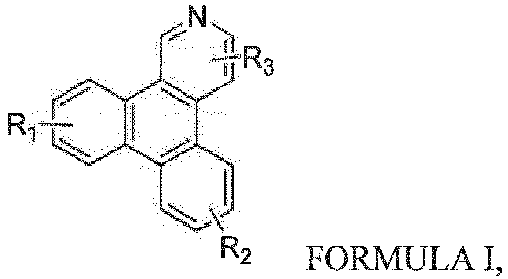
wherein R1, R2, and R3 are independently selected from the group consisting of hydrogen, alkyl, alkoxy, amino, alkenyl, alkynyl, arylkyl, aryl, and heteroaryl; and
wherein at least one of R1, R2, and R3 is an aryl or heteroaryl. - 2. The compound of aspect 1, wherein the compound has the formula:

wherein the compound is not coordinated to a metal. - 3. The compound of aspect 1, wherein R3 is a substitution ortho to the nitrogen.
- 4. The compound of aspect 1, wherein R1 is selected from the group consisting of alkyl, alkoxy, amino, alkenyl, alkynyl, arylkyl, aryl, and heteroaryl.
- 5. The compound of aspect 1, wherein R1 is an aryl or a heteroaryl.
- 6. The compound of aspect 1, wherein R2 is selected from the group consisting of alkyl, alkoxy, amino, alkenyl, alkynyl, arylkyl, aryl, and heteroaryl.
- 7. The compound of aspect 1, wherein R2 is an aryl of heteroaryl.
- 8. The compound of aspect 1, wherein R3 is selected from the group consisting of alkyl, alkoxy, amino, alkenyl, alkynyl, arylkyl, aryl, and heteroaryl.
- 9. The compound of aspect 1, wherein R3 is an aryl or heteroaryl.
- 10. The compound of aspect 1, wherein each of R1, R2, and R3 is an aryl or heteroaryl.
- 11. The compound of aspect 1, wherein the compound is selected from the group consisting of Compounds 1G to 70G defined above,
wherein R'3, R4, R5, R6, R7, and R8 may represent mono, di, tri, tetra, or penta substitutions; and
wherein R'3, R4, R5, R6, R7, and R8 are independently selected from the group consisting of hydrogen, alkyl, alkoxy, amino, alkenyl, alkynyl, arylkyl, aryl, and heteroaryl. - 12. The compound of aspect 1, wherein R1, R2, R3, R4, R5, R6, R7, and R8 are hydrogen.
- 13. The compound of aspect 1, wherein the compound comprises a ligand L having the formula:

wherein RA may represent a mono, di, tri, or tetra substitution;
wherein RA is selected from the group consisting of hydrogen, alkyl, alkoxy, amino, alkenyl, alkynyl, arylkyl, aryl, and heteroaryl; and
wherein the ligand L is coordinated to a metal having an atomic number greater than 40. - 14. The compound of aspect 13, wherein the metal is Ir.
- 15. The compound of aspect 14, wherein the ligand L is included in a homoleptic compound.
- 16. The compound of aspect 14, wherein the ligand L is included in a heteroleptic compound.
- 17. The compound of aspect 16, wherein the compound has the formula (L)n(L')3-nIr:
- wherein n is 1 or 2;
- wherein L' is selected from the group consisting of:

wherein R'1 and R'2 is selected from the group consisting of hydrogen, alkyl, alkoxy, amino, alkenyl, alkynyl, arylkyl, aryl, and heteroaryl; and
wherein-L has a different structure than L'.
- 18. The compound of aspect 17, wherein n is 1.
- 19. The compound of aspect 17, wherein n is 2.
- 20. The compound of aspect 13, wherein the ligand L is selected from the group consisting of Compounds 71 G to 78G defined above,
wherein R4 and R5 may represent mono, di, tri, tetra, or penta substitutions; and
wherein R4 and R5 are independently selected from the group consisting of hydrogen, alkyl, alkoxy, amino, alkenyl, alkynyl, arylkyl, aryl, and heteroaryl. - 21. The compound of aspect 1, wherein the ligand L is selected from the group consisting of:


- 22. The compound of aspect 1, wherein the compound is selected from the group consisting of:


- 23. The compound of aspect 1, wherein the compound is selected from the group consisting of:
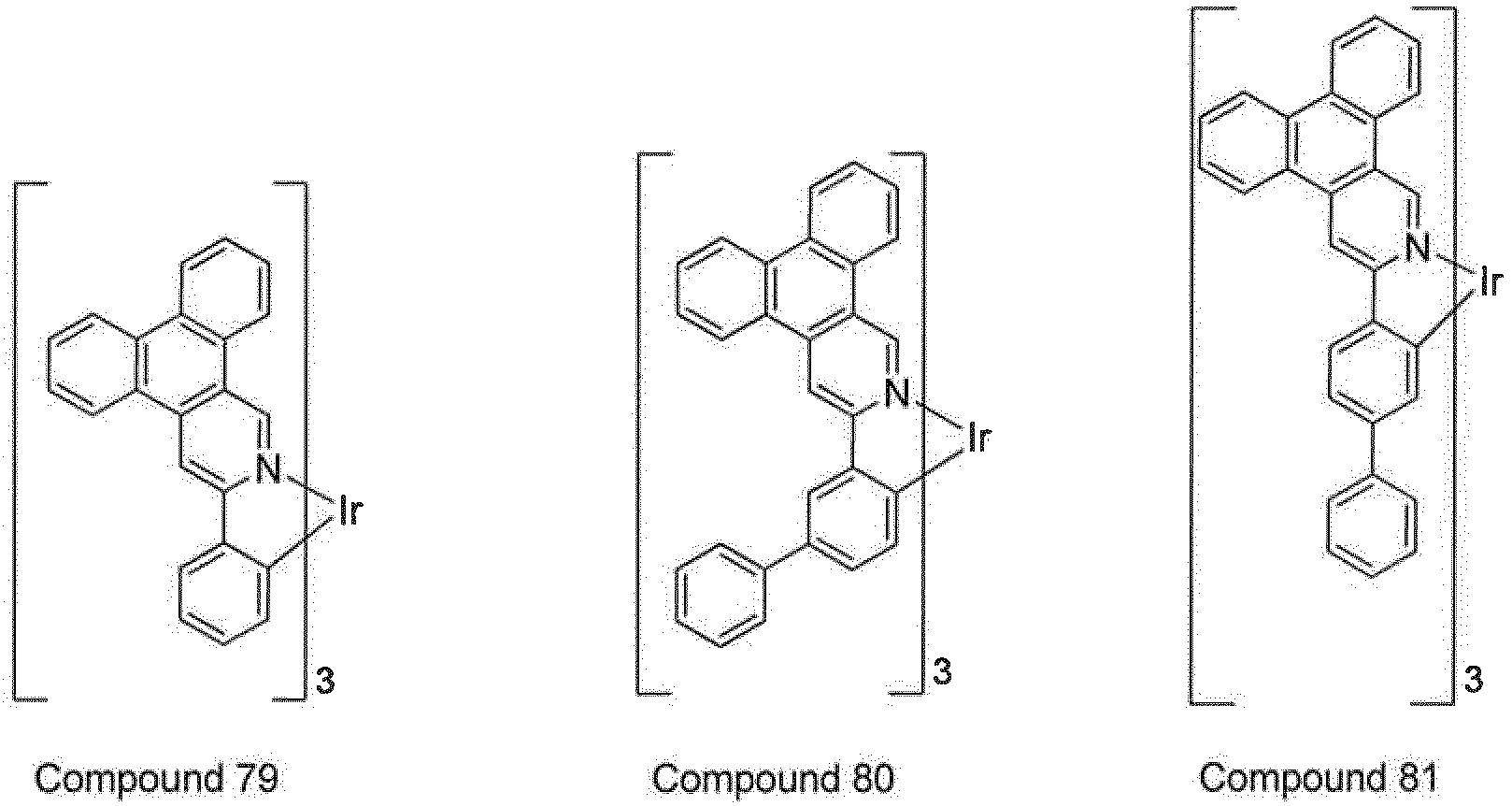


- 24. An organic light emitting device, comprising:
- an anode;
- a cathode; and
- a first organic layer, disposed between the anode and the cathode, the first organic layer further comprising a compound that includes the structure:

wherein R1, R2, and R3 are independently selected from the group consisting of hydrogen, alkyl, alkoxy, amino, alkenyl, alkynyl, arylkyl, aryl, and heteroaryl; and
wherein at least one of R1, R2, and R3 is an aryl or heteroaryl.
- 25. The device of aspect 24, wherein the compound has the formula:

wherein the compound is not coordinated to a metal. - 26. The device of aspect 25, wherein the compound is selected from the group consisting of Compounds 1 G to 70G defined above,
wherein R'3, R5, R6, R7, and R8 may represent mono, di, tri, tetra, or penta substitutions; and
wherein R'3, R4, R5, R6, R7, and R8 are independently selected from the group consisting of hydrogen, alkyl, alkoxy, amino, alkenyl, alkynyl, arylkyl, aryl, and heteroaryl. - 27. The device of aspect 24, wherein the first organic layer is an emissive layer and the compound including the structure FORMULA I is a host.
- 28. The device of aspect 27, wherein the first organic layer further comprises an emitting dopant.
- 29. The device of aspect 28, wherein the emitting dopant has the formula:

wherein Rx and Ry are independently selected from the group consisting of hydrogen, alkyl, and aryl. - 30. The device of aspect 24, wherein the compound comprises a ligand L having the formula:

wherein RA may represent a mono, di, tri, or tetra substitution;
wherein RA is selected from the group consisting of hydrogen, alkyl, alkoxy, amino, alkenyl, alkynyl, arylkyl, aryl, and heteroaryl; and
wherein the ligand L is coordinated to a metal having an atomic number greater than 40. - 31. The aspect of claim 30; wherein the ligand L is selected from the group consisting of Compounds 71G to 78G defined above,
wherein R4 and R5 may represent mono, di, tri, tetra, or penta substitutions; and
wherein R4 and R5 are independently selected from the group consisting of hydrogen, alkyl, alkoxy, amino, alkenyl, alkynyl, aryl, and heteroaryl. - 32. The device of aspect 30, wherein the compound is selected from the group consisting of:
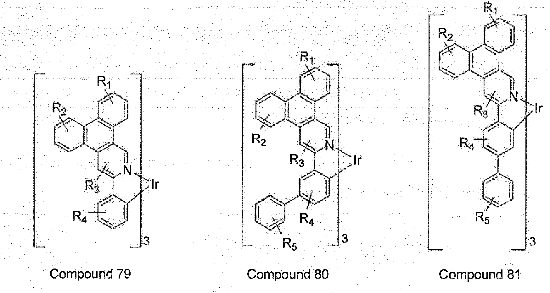


- 33. The device of aspect 30, wherein the first organic layer is an emissive layer and the compound including the structure FORMULA II is an emitting dopant.
- 34. The device of aspect 33, wherein the first organic layer further comprises a host material.
- 35. The device of aspect 24, wherein the device has a second organic layer that is a non-emissive layer and the compound including the structure FORMULA II is a non-emissive material in the second organic layer.
- 36. The device of aspect 35, wherein the second organic layer is a hole injection or transport layer and the compound including the structure FORMULA II is a hole injection or transport material in the second organic layer.
- 37. A consumer product comprising a device, the device further comprising:
- an anode;
- a cathode; and
- a first organic layer, disposed between the anode and the cathode, the first organic layer further comprising a compound that includes the structure:

wherein R1, R2, and R3 are independently selected from the group consisting of alkyl, alkoxy, amino, alkenyl, alkynyl, arylkyl, aryl, heteroaryl and hydrogen; and
wherein at least one of R1, R2, and R3 is an aryl or heteroaryl,
Claims (23)
- A compound including the structure:

wherein R1, R2, and R3 are independently selected from the group consisting of hydrogen, alkyl, alkoxy, amino, alkenyl, alkynyl, arylkyl, aryl, and heteroaryl; and
wherein at least one of R1, R2, and R3 is an aryl or heteroaryl. - The compound of claim 1, wherein the compound has the formula:

wherein the compound is not coordinated to a metal. - The compound of claim 1 or 2, wherein R3 is a substitution ortho to the nitrogen.
- The compound of any of the preceding claims, wherein R1 is selected from the group consisting of alkyl, alkoxy, amino, alkenyl, alkynyl, arylkyl, aryl, and heteroaryl, preferably R1 is an aryl or heteroaryl.
- The compound of any of the preceding claims, wherein R2 is selected from the group consisting of alkyl, alkoxy, amino, alkenyl, alkynyl, arylkyl, aryl, and heteroaryl, preferably R2 is an aryl of heteroaryl.
- The compound of any of the preceding claims, wherein R3 is selected from the group consisting of alkyl, alkoxy, amino, alkenyl, alkynyl, arylkyl, aryl, and heteroaryl, preferably R3 is an aryl or heteroaryl.
- The compound of any of the preceding claims, wherein each of R1, R2, and R3 is an aryl or heteroaryl.
- The compound of any of the preceding claims, wherein the compound is selected from the group consisting of:


wherein R'3, R4, R5, R7, and R8 are independently selected from the group consisting of alkyl, alkoxy, amino, alkenyl, alkynyl, arylkyl, aryl, and heteroaryl. - The compound of claim 1, wherein the compound comprises a ligand L having the formula:

wherein RA may represent a mono, di, tri, or tetra substitution;
wherein RA is selected from the group consisting of hydrogen, alkyl, alkoxy, amino, alkenyl, alkynyl, arylkyl, aryl, and heteroaryl; and
wherein the ligand L is coordinated to a metal having an atomic number greater than 40. - The compound of claim 9, wherein the metal is Ir, and preferably the ligand L is included in a homoleptic compound or in a heteroleptic compound.
- The compound of claim 10, wherein the compound has the formula. (L)n(L')3-nIr:wherein n is 1 or 2;wherein L' is selected from the group consisting of:
 wherein R'1 and R'2 may represent a mono, di, tri, or tetra substitution;wherein R'1 and R'2 is selected, from the group consisting of hydrogen, alkyl, alkoxy, amino, alkenyl, alkynyl, arylkyl, aryl, and heteroaryl; andwherein L has a different structure than L'.
 - The compound of claim 9, wherein the ligand L is selected from the group consisting of:


wherein and R5 are independently selected from the group consisting of hydrogen, alkyl, alkoxy, amino, alkenyl, alkynyl, arylkyl, aryl, and heteroaryl,
preferably the ligand L is selected from the group consisting of:


- The compound of claim 1, wherein the compound is selected from the group consisting of:


- An organic light emitting device, comprising:an anode;a cathode; anda first organic layer, disposed between the anode and the cathode, the first organic layer further comprising a compound that includes the structure:
 wherein R1, R2, and R3 may represent mono, di, tri, or tetra substitutions;wherein R1, R2, and R3 are independently selected from the group consisting of hydrogen, alkyl, alkoxy, amino, alkenyl, alkynyl, arylkyl, aryl, and heteroaryl; andwherein at least one of R1, R2, and R3 is an aryl or heteroaryl.
 - The device of claim 14, wherein the compound has the formula:

wherein the compound is not coordinated to a metal,
preferably the compound is selected from the group consisting of:


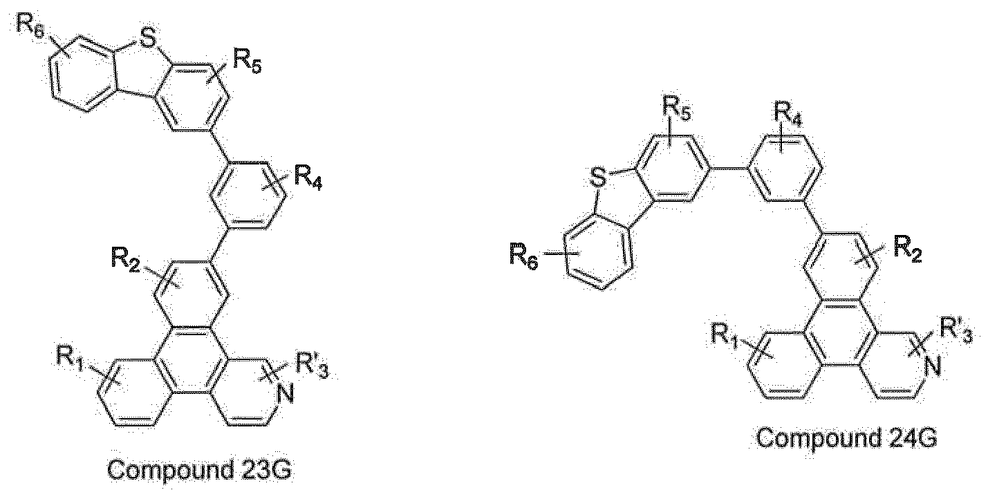


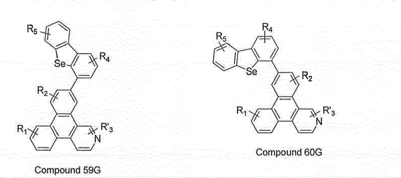


wherein R'3, R4, R5, R6, R7, and R8 are independently selected from the group consisting of alkyl, alkoxy, amino, alkenyl, alkynyl, arylkyl, aryl, and heteroaryl. - The device of claim 14, wherein the first organic layer is an emissive layer and the compound including the structure FORMULA I is a host.
- The device of claim 16, wherein the first organic layer further comprises an emitting dopant,
preferably the emitting dopant has the formula:
wherein Rx and Ry are independently selected from the group consisting of hydrogen, alkyl, and aryl. - The device, of claim 14, wherein the compound, comprises a ligand L having the formula:

wherein RA may represent a mono, di, tri, or terra substitution;
wherein RA is selected from the group consisting of hydrogen, alkyl, alkoxy, amino, alkenyl, alkynyl, arylkyl, aryl, and heteroaryl; and
wherein the ligand L is coordinated to a metal having an atomic number greater than 40. - The device of claim 18, wherein the ligand L is selected from the group consisting of:


wherein R4 and R5 are independently selected from the group consisting of hydrogen, alkyl, alkoxy, amino, alkenyl, alkynyl, aryl, and heteroaryl. - The device of claim 18; wherein the compound is selected from the group consisting of:


- The device of claim 18, wherein the first organic layer is an emissive layer and the compound including the structure FORMULA II is an emitting dopant,
wherein preferably the first organic layer further comprises a host material. - The device of claim 14, wherein the device has a second organic layer that is a non-emissive layer and the compound including the structure FORMULA II is a non-emissive material in the second organic layer,
wherein preferably the second organic layer is a hole injection or transport layer and the compound including the structure FORMULA II is a hole injection or transport material in the second organic layer. - A consumer product comprising a device, the device further comprising:an anode;a cathode; anda first organic layer, disposed between the anode and the cathode, the first organic layer further comprising a compound according to any one of claims 1 to 13.
Applications Claiming Priority (3)
| Application Number | Priority Date | Filing Date | Title |
|---|---|---|---|
| US17743509P | 2009-05-12 | 2009-05-12 | |
| EP10720077.6A EP2429997B1 (en) | 2009-05-12 | 2010-05-12 | 2-azatriphenylene materials for organic light emitting diodes |
| US12/778,362 US9005771B2 (en) | 2009-05-12 | 2010-05-12 | 2-azatriphenylene materials for organic light emitting diodes |
Related Parent Applications (3)
| Application Number | Title | Priority Date | Filing Date |
|---|---|---|---|
| EP10720077.6A Division-Into EP2429997B1 (en) | 2009-05-12 | 2010-05-12 | 2-azatriphenylene materials for organic light emitting diodes |
| EP10720077.6A Division EP2429997B1 (en) | 2009-05-12 | 2010-05-12 | 2-azatriphenylene materials for organic light emitting diodes |
| EP10720077.6 Division | 2010-05-12 |
Publications (2)
| Publication Number | Publication Date |
|---|---|
| EP2520571A1 true EP2520571A1 (en) | 2012-11-07 |
| EP2520571B1 EP2520571B1 (en) | 2016-08-17 |
Family
ID=42246255
Family Applications (2)
| Application Number | Title | Priority Date | Filing Date |
|---|---|---|---|
| EP12178748.5A Active EP2520571B1 (en) | 2009-05-12 | 2010-05-12 | 2-azatriphenylene materials for organic light emitting diodes |
| EP10720077.6A Active EP2429997B1 (en) | 2009-05-12 | 2010-05-12 | 2-azatriphenylene materials for organic light emitting diodes |
Family Applications After (1)
| Application Number | Title | Priority Date | Filing Date |
|---|---|---|---|
| EP10720077.6A Active EP2429997B1 (en) | 2009-05-12 | 2010-05-12 | 2-azatriphenylene materials for organic light emitting diodes |
Country Status (7)
| Country | Link |
|---|---|
| US (1) | US9005771B2 (en) |
| EP (2) | EP2520571B1 (en) |
| JP (2) | JP5937002B2 (en) |
| KR (2) | KR101884581B1 (en) |
| CN (2) | CN107325089B (en) |
| TW (1) | TWI541234B (en) |
| WO (1) | WO2010132524A1 (en) |
Cited By (3)
| Publication number | Priority date | Publication date | Assignee | Title |
|---|---|---|---|---|
| US9309223B2 (en) | 2011-07-08 | 2016-04-12 | Semiconductor Energy Laboratory Co., Ltd. | Heterocyclic compound, light-emitting element, light-emitting device, electronic device, and lighting device |
| US9899608B2 (en) | 2010-03-01 | 2018-02-20 | Semiconductor Energy Laboratory Co., Ltd. | Heterocyclic compound, light-emitting element, light-emitting device, electronic device, and lighting device |
| US9960368B2 (en) | 2011-02-01 | 2018-05-01 | Semiconductor Energy Laboratory Co., Ltd. | Heterocyclic compound |
Families Citing this family (42)
| Publication number | Priority date | Publication date | Assignee | Title |
|---|---|---|---|---|
| JP5305637B2 (en) | 2007-11-08 | 2013-10-02 | キヤノン株式会社 | Organometallic complex, organic light emitting device using the same, and display device |
| JP5604848B2 (en) * | 2009-10-19 | 2014-10-15 | コニカミノルタ株式会社 | ORGANIC ELECTROLUMINESCENT ELEMENT MATERIAL, ORGANIC ELECTROLUMINESCENT ELEMENT, LIGHTING DEVICE AND DISPLAY DEVICE |
| DE102010048608A1 (en) | 2010-10-15 | 2012-04-19 | Merck Patent Gmbh | Materials for organic electroluminescent devices |
| CN102127015B (en) * | 2011-01-13 | 2013-06-19 | 北京交通大学 | Perylene ring bridged benzophenanthrene compound and preparation method thereof |
| US8415031B2 (en) * | 2011-01-24 | 2013-04-09 | Universal Display Corporation | Electron transporting compounds |
| US9067916B2 (en) * | 2011-02-01 | 2015-06-30 | Semiconductor Energy Laboratory Co., Ltd. | Heterocyclic compound |
| KR20130007162A (en) * | 2011-06-29 | 2013-01-18 | 삼성디스플레이 주식회사 | Novel heterocyclic compound and organic light emitting device containing same |
| DE112012003638B4 (en) * | 2011-08-31 | 2023-01-19 | Semiconductor Energy Laboratory Co., Ltd. | Light-emitting element, light-emitting device, electronic device, lighting device, and heterocyclic compound |
| JP2013063963A (en) | 2011-08-31 | 2013-04-11 | Semiconductor Energy Lab Co Ltd | Heterocyclic compound, light-emitting element, light-emitting element, electronic device and lighting device |
| US9096578B2 (en) * | 2011-11-04 | 2015-08-04 | Semiconductor Energy Laboratory Co., Ltd. | Dibenzol[f,h]quinoxaline compound, light-emitting element, light-emitting device, electronic device, and lighting device |
| US8766531B1 (en) * | 2012-12-14 | 2014-07-01 | Universal Display Corporation | Wearable display |
| JP5818870B2 (en) * | 2012-12-27 | 2015-11-18 | キヤノン株式会社 | Organic light emitting device and display device |
| JP6253971B2 (en) * | 2012-12-28 | 2017-12-27 | 株式会社半導体エネルギー研究所 | LIGHT EMITTING ELEMENT, LIGHT EMITTING DEVICE, ELECTRONIC DEVICE, AND LIGHTING DEVICE |
| JP6071569B2 (en) * | 2013-01-17 | 2017-02-01 | キヤノン株式会社 | Organic light emitting device |
| JP6222931B2 (en) * | 2013-01-21 | 2017-11-01 | キヤノン株式会社 | Organic light emitting device |
| JP5984689B2 (en) | 2013-01-21 | 2016-09-06 | キヤノン株式会社 | Organometallic complex and organic light emitting device using the same |
| KR102162793B1 (en) | 2013-03-05 | 2020-10-08 | 삼성디스플레이 주식회사 | Compound and organic light emitting device comprising the same |
| US9537106B2 (en) * | 2013-05-09 | 2017-01-03 | Universal Display Corporation | Organic electroluminescent materials and devices |
| KR102188028B1 (en) | 2013-06-18 | 2020-12-08 | 삼성디스플레이 주식회사 | Organic light emitting device |
| JP6386299B2 (en) | 2013-08-30 | 2018-09-05 | 株式会社半導体エネルギー研究所 | Organic compounds for light emitting devices |
| KR102167048B1 (en) * | 2013-12-03 | 2020-10-19 | 삼성디스플레이 주식회사 | Compound and organic light emitting device comprising same |
| US9755159B2 (en) * | 2014-01-23 | 2017-09-05 | Universal Display Corporation | Organic materials for OLEDs |
| KR102326623B1 (en) | 2014-03-18 | 2021-11-16 | 메르크 파텐트 게엠베하 | Organic electroluminescent device |
| DE102015017428B4 (en) | 2014-07-25 | 2025-10-09 | Semiconductor Energy Laboratory Co.,Ltd. | Light-emitting element, light-emitting device, electronic device and lighting device |
| CN105399749B (en) * | 2015-10-21 | 2017-10-10 | 中节能万润股份有限公司 | A kind of new OLED electron transport materials and its application |
| CN108137633A (en) * | 2015-12-04 | 2018-06-08 | 广州华睿光电材料有限公司 | Metal organic complex, high polymer, mixture, composition and organic electronic device |
| US12082500B2 (en) | 2015-12-21 | 2024-09-03 | Samsung Display Co., Ltd. | Condensed cyclic compound and organic light-emitting device including the same |
| KR102008895B1 (en) * | 2016-05-31 | 2019-08-08 | 삼성에스디아이 주식회사 | Organic compound for optoelectric device and organic optoelectric device and display device |
| KR102138823B1 (en) * | 2017-12-27 | 2020-07-28 | 삼성에스디아이 주식회사 | Organic optoelectric device and display device |
| US11515493B2 (en) | 2018-01-11 | 2022-11-29 | Universal Display Corporation | Organic electroluminescent materials and devices |
| US11557733B2 (en) | 2018-03-12 | 2023-01-17 | Universal Display Corporation | Organic electroluminescent materials and devices |
| US12291540B2 (en) | 2019-03-29 | 2025-05-06 | Samsung Electronics Co., Ltd. | Organometallic compound, organic light-emitting device including the same, and electronic apparatus including the organic light-emitting device |
| EP3715352B1 (en) * | 2019-03-29 | 2025-07-30 | Samsung Electronics Co., Ltd. | Organometallic compound, organic light-emitting device including the same, and electronic apparatus including the organic light-emitting device |
| CN112250667B (en) * | 2019-07-22 | 2024-03-08 | 固安鼎材科技有限公司 | Organic compound, application thereof and organic electroluminescent device using same |
| CN110698517B (en) * | 2019-09-27 | 2022-05-20 | 吉林奥来德光电材料股份有限公司 | Iridium metal complex and its preparation method and organic electroluminescent device |
| CN112592371A (en) * | 2019-10-02 | 2021-04-02 | 环球展览公司 | Organic electroluminescent material and device |
| US12486296B2 (en) * | 2019-10-02 | 2025-12-02 | Universal Display Corporation | Organic electroluminescent materials and devices |
| CN110759950B (en) * | 2019-10-31 | 2022-03-15 | 吉林奥来德光电材料股份有限公司 | Organic phosphorus luminescent material, preparation method thereof and organic electroluminescent device prepared from organic phosphorus luminescent material |
| KR102761436B1 (en) * | 2019-12-20 | 2025-02-03 | 삼성전자주식회사 | Organometallic compound and organic light emitting device including the same |
| US12152042B2 (en) | 2020-05-14 | 2024-11-26 | Samsung Electronics Co., Ltd. | Organometallic compound, organic light-emitting device including the same, and electronic apparatus including the organic light-emitting device |
| CN111825723A (en) * | 2020-07-15 | 2020-10-27 | 奥来德(上海)光电材料科技有限公司 | Organic iridium metal complex and preparation method and application thereof |
| CN111690019A (en) * | 2020-07-15 | 2020-09-22 | 奥来德(上海)光电材料科技有限公司 | Organic iridium metal complex and preparation method and application thereof |
Citations (22)
| Publication number | Priority date | Publication date | Assignee | Title |
|---|---|---|---|---|
| US4769292A (en) | 1987-03-02 | 1988-09-06 | Eastman Kodak Company | Electroluminescent device with modified thin film luminescent zone |
| US5247190A (en) | 1989-04-20 | 1993-09-21 | Cambridge Research And Innovation Limited | Electroluminescent devices |
| US5703436A (en) | 1994-12-13 | 1997-12-30 | The Trustees Of Princeton University | Transparent contacts for organic devices |
| US5707745A (en) | 1994-12-13 | 1998-01-13 | The Trustees Of Princeton University | Multicolor organic light emitting devices |
| US5834893A (en) | 1996-12-23 | 1998-11-10 | The Trustees Of Princeton University | High efficiency organic light emitting devices with light directing structures |
| US5844363A (en) | 1997-01-23 | 1998-12-01 | The Trustees Of Princeton Univ. | Vacuum deposited, non-polymeric flexible organic light emitting devices |
| US6013982A (en) | 1996-12-23 | 2000-01-11 | The Trustees Of Princeton University | Multicolor display devices |
| US6087196A (en) | 1998-01-30 | 2000-07-11 | The Trustees Of Princeton University | Fabrication of organic semiconductor devices using ink jet printing |
| US6091195A (en) | 1997-02-03 | 2000-07-18 | The Trustees Of Princeton University | Displays having mesa pixel configuration |
| US6097147A (en) | 1998-09-14 | 2000-08-01 | The Trustees Of Princeton University | Structure for high efficiency electroluminescent device |
| US6294398B1 (en) | 1999-11-23 | 2001-09-25 | The Trustees Of Princeton University | Method for patterning devices |
| US6303238B1 (en) | 1997-12-01 | 2001-10-16 | The Trustees Of Princeton University | OLEDs doped with phosphorescent compounds |
| US6337102B1 (en) | 1997-11-17 | 2002-01-08 | The Trustees Of Princeton University | Low pressure vapor phase deposition of organic thin films |
| US20030230980A1 (en) | 2002-06-18 | 2003-12-18 | Forrest Stephen R | Very low voltage, high efficiency phosphorescent oled in a p-i-n structure |
| US20040174116A1 (en) | 2001-08-20 | 2004-09-09 | Lu Min-Hao Michael | Transparent electrodes |
| EP1555269A1 (en) * | 2004-01-13 | 2005-07-20 | LG Electronics Inc. | Phenyl pyridine-iridium metal complex compounds for organic electroluminescent device, process for preparing the compounds, and organic electroluminescent device using the compounds |
| US20060280965A1 (en) | 2005-05-31 | 2006-12-14 | Raymond Kwong | Triphenylene hosts in phosphorescent light emitting diodes |
| JP2007189001A (en) | 2006-01-12 | 2007-07-26 | Konica Minolta Holdings Inc | ORGANIC ELECTROLUMINESCENT ELEMENT MATERIAL, ORGANIC ELECTROLUMINESCENT ELEMENT, DISPLAY DEVICE AND LIGHTING DEVICE |
| US7279704B2 (en) | 2004-05-18 | 2007-10-09 | The University Of Southern California | Complexes with tridentate ligands |
| WO2009021126A2 (en) * | 2007-08-08 | 2009-02-12 | Universal Display Corporation | Benzo-fused thiophene or benzo-fused furan compounds comprising a triphenylene group |
| WO2009060995A1 (en) * | 2007-11-08 | 2009-05-14 | Canon Kabushiki Kaisha | Organic metal complex, and organic light emitting device and display apparatus using the same |
| EP2103665A1 (en) * | 2008-03-19 | 2009-09-23 | Gracel Display Inc. | Novel organic electroluminescent compounds and organic electroluminescent device using the same |
Family Cites Families (42)
| Publication number | Priority date | Publication date | Assignee | Title |
|---|---|---|---|---|
| US5061569A (en) | 1990-07-26 | 1991-10-29 | Eastman Kodak Company | Electroluminescent device with organic electroluminescent medium |
| DE69412567T2 (en) | 1993-11-01 | 1999-02-04 | Hodogaya Chemical Co., Ltd., Tokio/Tokyo | Amine compound and electroluminescent device containing it |
| AU681934B2 (en) | 1995-03-14 | 1997-09-11 | Kalford Pty Ltd | A hinge |
| US6830828B2 (en) | 1998-09-14 | 2004-12-14 | The Trustees Of Princeton University | Organometallic complexes as phosphorescent emitters in organic LEDs |
| US6458475B1 (en) | 1999-11-24 | 2002-10-01 | The Trustee Of Princeton University | Organic light emitting diode having a blue phosphorescent molecule as an emitter |
| US20020121638A1 (en) | 2000-06-30 | 2002-09-05 | Vladimir Grushin | Electroluminescent iridium compounds with fluorinated phenylpyridines, phenylpyrimidines, and phenylquinolines and devices made with such compounds |
| JP3812730B2 (en) | 2001-02-01 | 2006-08-23 | 富士写真フイルム株式会社 | Transition metal complex and light emitting device |
| US7431968B1 (en) | 2001-09-04 | 2008-10-07 | The Trustees Of Princeton University | Process and apparatus for organic vapor jet deposition |
| US6835469B2 (en) | 2001-10-17 | 2004-12-28 | The University Of Southern California | Phosphorescent compounds and devices comprising the same |
| US7166368B2 (en) | 2001-11-07 | 2007-01-23 | E. I. Du Pont De Nemours And Company | Electroluminescent platinum compounds and devices made with such compounds |
| US6863997B2 (en) | 2001-12-28 | 2005-03-08 | The Trustees Of Princeton University | White light emitting OLEDs from combined monomer and aggregate emission |
| KR100691543B1 (en) | 2002-01-18 | 2007-03-09 | 주식회사 엘지화학 | New material for electron transport and organic light emitting device using the same |
| US6687266B1 (en) | 2002-11-08 | 2004-02-03 | Universal Display Corporation | Organic light emitting materials and devices |
| US7345301B2 (en) | 2003-04-15 | 2008-03-18 | Merck Patent Gmbh | Mixtures of matrix materials and organic semiconductors capable of emission, use of the same and electronic components containing said mixtures |
| US7029765B2 (en) | 2003-04-22 | 2006-04-18 | Universal Display Corporation | Organic light emitting devices having reduced pixel shrinkage |
| CN100483779C (en) | 2003-05-29 | 2009-04-29 | 新日铁化学株式会社 | organic electroluminescent element |
| JP2005011610A (en) | 2003-06-18 | 2005-01-13 | Nippon Steel Chem Co Ltd | Organic electroluminescence device |
| US20050025993A1 (en) | 2003-07-25 | 2005-02-03 | Thompson Mark E. | Materials and structures for enhancing the performance of organic light emitting devices |
| TWI390006B (en) | 2003-08-07 | 2013-03-21 | Nippon Steel Chemical Co | Organic EL materials with aluminum clamps |
| US20060269780A1 (en) | 2003-09-25 | 2006-11-30 | Takayuki Fukumatsu | Organic electroluminescent device |
| TW200531592A (en) | 2004-03-15 | 2005-09-16 | Nippon Steel Chemical Co | Organic electroluminescent device |
| US7491823B2 (en) | 2004-05-18 | 2009-02-17 | The University Of Southern California | Luminescent compounds with carbene ligands |
| WO2005123873A1 (en) | 2004-06-17 | 2005-12-29 | Konica Minolta Holdings, Inc. | Organic electroluminescent device material, organic electroluminescent device, display and illuminating device |
| US20060008670A1 (en) | 2004-07-06 | 2006-01-12 | Chun Lin | Organic light emitting materials and devices |
| EP2178348B1 (en) | 2004-07-23 | 2012-11-21 | Konica Minolta Holdings, Inc. | Organic electroluminescent element, display and illuminator |
| DE102004057072A1 (en) | 2004-11-25 | 2006-06-01 | Basf Ag | Use of Transition Metal Carbene Complexes in Organic Light Emitting Diodes (OLEDs) |
| JPWO2006082742A1 (en) | 2005-02-04 | 2008-06-26 | コニカミノルタホールディングス株式会社 | ORGANIC ELECTROLUMINESCENT ELEMENT MATERIAL, ORGANIC ELECTROLUMINESCENT ELEMENT, DISPLAY DEVICE AND LIGHTING DEVICE |
| KR100803125B1 (en) | 2005-03-08 | 2008-02-14 | 엘지전자 주식회사 | Red phosphorescent compound and organic light emitting device using the same |
| JP5125502B2 (en) | 2005-03-16 | 2013-01-23 | コニカミノルタホールディングス株式会社 | Organic electroluminescence element material, organic electroluminescence element |
| WO2006103874A1 (en) | 2005-03-29 | 2006-10-05 | Konica Minolta Holdings, Inc. | Organic electroluminescent device material, organic electroluminescent device, display and illuminating device |
| GB2439030B (en) | 2005-04-18 | 2011-03-02 | Konica Minolta Holdings Inc | Organic electroluminescent device, display and illuminating device |
| US9051344B2 (en) | 2005-05-06 | 2015-06-09 | Universal Display Corporation | Stability OLED materials and devices |
| CN101193875B (en) | 2005-06-07 | 2011-05-11 | 新日铁化学株式会社 | Organic metal complex and organic electroluminescent device using same |
| US20090039771A1 (en) | 2005-07-01 | 2009-02-12 | Konica Minolta Holdings, Inc. | Organic electroluminescent element material, organic electroluminescent element, display device and lighting device |
| JP4887731B2 (en) | 2005-10-26 | 2012-02-29 | コニカミノルタホールディングス株式会社 | Organic electroluminescence element, display device and lighting device |
| WO2007063796A1 (en) | 2005-12-01 | 2007-06-07 | Nippon Steel Chemical Co., Ltd. | Organic electroluminescent device |
| EP1956022B1 (en) | 2005-12-01 | 2012-07-25 | Nippon Steel Chemical Co., Ltd. | Compound for organic electroluminescent element and organic electroluminescent element |
| CN101415718B (en) | 2006-02-10 | 2013-05-29 | 通用显示公司 | Cyclometallated imidazo[1,2-f]phenanthridine and diimidazo[1,2-a:1',2'-c]quinazoline ligands and their isoelectronic and benzocyclization analogs metal complexes |
| JP4823730B2 (en) | 2006-03-20 | 2011-11-24 | 新日鐵化学株式会社 | Luminescent layer compound and organic electroluminescent device |
| JP2010515255A (en) * | 2006-12-28 | 2010-05-06 | ユニバーサル ディスプレイ コーポレイション | Long-life phosphorescent organic light-emitting device (OLED) structure |
| ATE522588T1 (en) * | 2007-04-04 | 2011-09-15 | Basf Se | IRIDIUM-TRIPHENYLENE COMPLEXES AND THEIR USE IN OLEDS |
| KR20090010883A (en) * | 2007-07-23 | 2009-01-30 | 소니 가부시끼가이샤 | Organic electroluminescent device and display device |
-
2010
- 2010-05-11 TW TW099114982A patent/TWI541234B/en active
- 2010-05-12 KR KR1020177013084A patent/KR101884581B1/en active Active
- 2010-05-12 CN CN201710274122.3A patent/CN107325089B/en active Active
- 2010-05-12 EP EP12178748.5A patent/EP2520571B1/en active Active
- 2010-05-12 EP EP10720077.6A patent/EP2429997B1/en active Active
- 2010-05-12 JP JP2012510966A patent/JP5937002B2/en active Active
- 2010-05-12 KR KR1020117029712A patent/KR101738534B1/en active Active
- 2010-05-12 WO PCT/US2010/034479 patent/WO2010132524A1/en not_active Ceased
- 2010-05-12 CN CN2010800280229A patent/CN102482222A/en active Pending
- 2010-05-12 US US12/778,362 patent/US9005771B2/en active Active
-
2015
- 2015-12-08 JP JP2015239185A patent/JP6025959B2/en active Active
Patent Citations (23)
| Publication number | Priority date | Publication date | Assignee | Title |
|---|---|---|---|---|
| US4769292A (en) | 1987-03-02 | 1988-09-06 | Eastman Kodak Company | Electroluminescent device with modified thin film luminescent zone |
| US5247190A (en) | 1989-04-20 | 1993-09-21 | Cambridge Research And Innovation Limited | Electroluminescent devices |
| US5703436A (en) | 1994-12-13 | 1997-12-30 | The Trustees Of Princeton University | Transparent contacts for organic devices |
| US5707745A (en) | 1994-12-13 | 1998-01-13 | The Trustees Of Princeton University | Multicolor organic light emitting devices |
| US5834893A (en) | 1996-12-23 | 1998-11-10 | The Trustees Of Princeton University | High efficiency organic light emitting devices with light directing structures |
| US6013982A (en) | 1996-12-23 | 2000-01-11 | The Trustees Of Princeton University | Multicolor display devices |
| US5844363A (en) | 1997-01-23 | 1998-12-01 | The Trustees Of Princeton Univ. | Vacuum deposited, non-polymeric flexible organic light emitting devices |
| US6091195A (en) | 1997-02-03 | 2000-07-18 | The Trustees Of Princeton University | Displays having mesa pixel configuration |
| US6337102B1 (en) | 1997-11-17 | 2002-01-08 | The Trustees Of Princeton University | Low pressure vapor phase deposition of organic thin films |
| US6303238B1 (en) | 1997-12-01 | 2001-10-16 | The Trustees Of Princeton University | OLEDs doped with phosphorescent compounds |
| US6087196A (en) | 1998-01-30 | 2000-07-11 | The Trustees Of Princeton University | Fabrication of organic semiconductor devices using ink jet printing |
| US6097147A (en) | 1998-09-14 | 2000-08-01 | The Trustees Of Princeton University | Structure for high efficiency electroluminescent device |
| US6294398B1 (en) | 1999-11-23 | 2001-09-25 | The Trustees Of Princeton University | Method for patterning devices |
| US6468819B1 (en) | 1999-11-23 | 2002-10-22 | The Trustees Of Princeton University | Method for patterning organic thin film devices using a die |
| US20040174116A1 (en) | 2001-08-20 | 2004-09-09 | Lu Min-Hao Michael | Transparent electrodes |
| US20030230980A1 (en) | 2002-06-18 | 2003-12-18 | Forrest Stephen R | Very low voltage, high efficiency phosphorescent oled in a p-i-n structure |
| EP1555269A1 (en) * | 2004-01-13 | 2005-07-20 | LG Electronics Inc. | Phenyl pyridine-iridium metal complex compounds for organic electroluminescent device, process for preparing the compounds, and organic electroluminescent device using the compounds |
| US7279704B2 (en) | 2004-05-18 | 2007-10-09 | The University Of Southern California | Complexes with tridentate ligands |
| US20060280965A1 (en) | 2005-05-31 | 2006-12-14 | Raymond Kwong | Triphenylene hosts in phosphorescent light emitting diodes |
| JP2007189001A (en) | 2006-01-12 | 2007-07-26 | Konica Minolta Holdings Inc | ORGANIC ELECTROLUMINESCENT ELEMENT MATERIAL, ORGANIC ELECTROLUMINESCENT ELEMENT, DISPLAY DEVICE AND LIGHTING DEVICE |
| WO2009021126A2 (en) * | 2007-08-08 | 2009-02-12 | Universal Display Corporation | Benzo-fused thiophene or benzo-fused furan compounds comprising a triphenylene group |
| WO2009060995A1 (en) * | 2007-11-08 | 2009-05-14 | Canon Kabushiki Kaisha | Organic metal complex, and organic light emitting device and display apparatus using the same |
| EP2103665A1 (en) * | 2008-03-19 | 2009-09-23 | Gracel Display Inc. | Novel organic electroluminescent compounds and organic electroluminescent device using the same |
Non-Patent Citations (4)
| Title |
|---|
| BALDO ET AL.: "Highly Efficient Phosphorescent Emission from Organic Electroluminescent Devices", NATURE, vol. 395, 1998, pages 151 - 154, XP001002103, DOI: doi:10.1038/25954 |
| BALDO ET AL.: "Very high-efficiency green organic light-emitting devices based on electrophosphorescence", APPL. PHYS. LETT., vol. 75, no. 3, 1999, pages 4 - 6, XP012023409, DOI: doi:10.1063/1.124258 |
| HEWLINE, M. ET AL., SYNTHESIS, vol. 14, 2007, pages 2157 - 2163 |
| MCIVER A ET AL: "A general approach to triphenylenes and azatriphenylenes: total synthesis of dehydrotylophorine and tylophorine", CHEMICAL COMMUNICATIONS, no. 39, 21 October 2008 (2008-10-21), pages 4750 - 4652, XP009135250, ISSN: 1359-7345, DOI: 10.1039/b811068a * |
Cited By (5)
| Publication number | Priority date | Publication date | Assignee | Title |
|---|---|---|---|---|
| US9899608B2 (en) | 2010-03-01 | 2018-02-20 | Semiconductor Energy Laboratory Co., Ltd. | Heterocyclic compound, light-emitting element, light-emitting device, electronic device, and lighting device |
| US10224490B2 (en) | 2010-03-01 | 2019-03-05 | Semiconductor Energy Laboratory Co., Ltd. | Heterocyclic compound, light-emitting element, light-emitting device, electronic device, and lighting device |
| US9960368B2 (en) | 2011-02-01 | 2018-05-01 | Semiconductor Energy Laboratory Co., Ltd. | Heterocyclic compound |
| US9309223B2 (en) | 2011-07-08 | 2016-04-12 | Semiconductor Energy Laboratory Co., Ltd. | Heterocyclic compound, light-emitting element, light-emitting device, electronic device, and lighting device |
| US9843000B2 (en) | 2011-07-08 | 2017-12-12 | Semiconductor Energy Laboratory Co., Ltd. | Heterocyclic compound, light-emitting element, light-emitting device, electronic device, and lighting device |
Also Published As
| Publication number | Publication date |
|---|---|
| KR20170056035A (en) | 2017-05-22 |
| EP2429997A1 (en) | 2012-03-21 |
| CN107325089B (en) | 2021-07-13 |
| EP2429997B1 (en) | 2014-01-15 |
| US9005771B2 (en) | 2015-04-14 |
| KR101884581B1 (en) | 2018-08-01 |
| KR20120023780A (en) | 2012-03-13 |
| JP5937002B2 (en) | 2016-06-22 |
| CN102482222A (en) | 2012-05-30 |
| TWI541234B (en) | 2016-07-11 |
| TW201111347A (en) | 2011-04-01 |
| KR101738534B1 (en) | 2017-05-23 |
| JP2012526833A (en) | 2012-11-01 |
| CN107325089A (en) | 2017-11-07 |
| US20100289406A1 (en) | 2010-11-18 |
| JP2016104745A (en) | 2016-06-09 |
| EP2520571B1 (en) | 2016-08-17 |
| JP6025959B2 (en) | 2016-11-16 |
| WO2010132524A1 (en) | 2010-11-18 |
Similar Documents
| Publication | Publication Date | Title |
|---|---|---|
| EP2429997B1 (en) | 2-azatriphenylene materials for organic light emitting diodes | |
| US20230309376A1 (en) | Organic electroluminescent materials and devices | |
| EP2542644B1 (en) | Phosphorescent materials | |
| US9735377B2 (en) | Phosphorescent emitters and host materials with improved stability | |
| JP6316351B2 (en) | Pyridylcarbene phosphor photoluminescent material | |
| EP3081617B1 (en) | Blue emitter with high efficiency based on imidazo [1,2-f] phenanthridine iridium complexes | |
| JP6219466B2 (en) | Phosphorescent substance | |
| EP2703405B1 (en) | New materials with aza-dibenzothiophene or aza-dibenzofuran core for pholed | |
| EP2342305B1 (en) | Phosphorescent materials | |
| EP2424953B1 (en) | Iridium complex with methyl-d3 substitution | |
| EP2574613B1 (en) | Cyclometallated tetradentate Pt (II) complexes comprised of one or two imidazole rings with a twisted aryl group bonded to N-1 | |
| EP3401974B1 (en) | Host materials for phosphorescent oleds |
Legal Events
| Date | Code | Title | Description |
|---|---|---|---|
| PUAI | Public reference made under article 153(3) epc to a published international application that has entered the european phase |
Free format text: ORIGINAL CODE: 0009012 |
|
| 17P | Request for examination filed |
Effective date: 20120731 |
|
| AC | Divisional application: reference to earlier application |
Ref document number: 2429997 Country of ref document: EP Kind code of ref document: P |
|
| AK | Designated contracting states |
Kind code of ref document: A1 Designated state(s): AL AT BE BG CH CY CZ DE DK EE ES FI FR GB GR HR HU IE IS IT LI LT LU LV MC MK MT NL NO PL PT RO SE SI SK SM TR |
|
| 17Q | First examination report despatched |
Effective date: 20140124 |
|
| GRAP | Despatch of communication of intention to grant a patent |
Free format text: ORIGINAL CODE: EPIDOSNIGR1 |
|
| RIC1 | Information provided on ipc code assigned before grant |
Ipc: C07D 401/10 20060101ALI20150930BHEP Ipc: H01L 51/50 20060101ALI20150930BHEP Ipc: C07F 15/00 20060101ALI20150930BHEP Ipc: C07D 495/04 20060101ALI20150930BHEP Ipc: C07D 421/10 20060101ALI20150930BHEP Ipc: C09K 11/06 20060101ALI20150930BHEP Ipc: H01L 51/00 20060101ALI20150930BHEP Ipc: C07D 221/18 20060101AFI20150930BHEP Ipc: H05B 33/10 20060101ALI20150930BHEP Ipc: C07D 409/10 20060101ALI20150930BHEP Ipc: C07D 405/10 20060101ALI20150930BHEP |
|
| INTG | Intention to grant announced |
Effective date: 20151029 |
|
| GRAP | Despatch of communication of intention to grant a patent |
Free format text: ORIGINAL CODE: EPIDOSNIGR1 |
|
| INTG | Intention to grant announced |
Effective date: 20160315 |
|
| GRAS | Grant fee paid |
Free format text: ORIGINAL CODE: EPIDOSNIGR3 |
|
| GRAA | (expected) grant |
Free format text: ORIGINAL CODE: 0009210 |
|
| AC | Divisional application: reference to earlier application |
Ref document number: 2429997 Country of ref document: EP Kind code of ref document: P |
|
| AK | Designated contracting states |
Kind code of ref document: B1 Designated state(s): AL AT BE BG CH CY CZ DE DK EE ES FI FR GB GR HR HU IE IS IT LI LT LU LV MC MK MT NL NO PL PT RO SE SI SK SM TR |
|
| REG | Reference to a national code |
Ref country code: GB Ref legal event code: FG4D |
|
| REG | Reference to a national code |
Ref country code: CH Ref legal event code: EP |
|
| REG | Reference to a national code |
Ref country code: IE Ref legal event code: FG4D |
|
| REG | Reference to a national code |
Ref country code: AT Ref legal event code: REF Ref document number: 820924 Country of ref document: AT Kind code of ref document: T Effective date: 20160915 |
|
| REG | Reference to a national code |
Ref country code: DE Ref legal event code: R096 Ref document number: 602010035729 Country of ref document: DE |
|
| REG | Reference to a national code |
Ref country code: CH Ref legal event code: NV Representative=s name: GOTTSCHALK MAIWALD PATENTANWALTS- UND RECHTSAN, CH |
|
| REG | Reference to a national code |
Ref country code: NL Ref legal event code: MP Effective date: 20160817 |
|
| REG | Reference to a national code |
Ref country code: LT Ref legal event code: MG4D |
|
| REG | Reference to a national code |
Ref country code: AT Ref legal event code: MK05 Ref document number: 820924 Country of ref document: AT Kind code of ref document: T Effective date: 20160817 |
|
| PG25 | Lapsed in a contracting state [announced via postgrant information from national office to epo] |
Ref country code: IT Free format text: LAPSE BECAUSE OF FAILURE TO SUBMIT A TRANSLATION OF THE DESCRIPTION OR TO PAY THE FEE WITHIN THE PRESCRIBED TIME-LIMIT Effective date: 20160817 Ref country code: HR Free format text: LAPSE BECAUSE OF FAILURE TO SUBMIT A TRANSLATION OF THE DESCRIPTION OR TO PAY THE FEE WITHIN THE PRESCRIBED TIME-LIMIT Effective date: 20160817 Ref country code: NO Free format text: LAPSE BECAUSE OF FAILURE TO SUBMIT A TRANSLATION OF THE DESCRIPTION OR TO PAY THE FEE WITHIN THE PRESCRIBED TIME-LIMIT Effective date: 20161117 Ref country code: NL Free format text: LAPSE BECAUSE OF FAILURE TO SUBMIT A TRANSLATION OF THE DESCRIPTION OR TO PAY THE FEE WITHIN THE PRESCRIBED TIME-LIMIT Effective date: 20160817 Ref country code: FI Free format text: LAPSE BECAUSE OF FAILURE TO SUBMIT A TRANSLATION OF THE DESCRIPTION OR TO PAY THE FEE WITHIN THE PRESCRIBED TIME-LIMIT Effective date: 20160817 Ref country code: LT Free format text: LAPSE BECAUSE OF FAILURE TO SUBMIT A TRANSLATION OF THE DESCRIPTION OR TO PAY THE FEE WITHIN THE PRESCRIBED TIME-LIMIT Effective date: 20160817 |
|
| PG25 | Lapsed in a contracting state [announced via postgrant information from national office to epo] |
Ref country code: GR Free format text: LAPSE BECAUSE OF FAILURE TO SUBMIT A TRANSLATION OF THE DESCRIPTION OR TO PAY THE FEE WITHIN THE PRESCRIBED TIME-LIMIT Effective date: 20161118 Ref country code: LV Free format text: LAPSE BECAUSE OF FAILURE TO SUBMIT A TRANSLATION OF THE DESCRIPTION OR TO PAY THE FEE WITHIN THE PRESCRIBED TIME-LIMIT Effective date: 20160817 Ref country code: SE Free format text: LAPSE BECAUSE OF FAILURE TO SUBMIT A TRANSLATION OF THE DESCRIPTION OR TO PAY THE FEE WITHIN THE PRESCRIBED TIME-LIMIT Effective date: 20160817 Ref country code: PL Free format text: LAPSE BECAUSE OF FAILURE TO SUBMIT A TRANSLATION OF THE DESCRIPTION OR TO PAY THE FEE WITHIN THE PRESCRIBED TIME-LIMIT Effective date: 20160817 Ref country code: PT Free format text: LAPSE BECAUSE OF FAILURE TO SUBMIT A TRANSLATION OF THE DESCRIPTION OR TO PAY THE FEE WITHIN THE PRESCRIBED TIME-LIMIT Effective date: 20161219 Ref country code: ES Free format text: LAPSE BECAUSE OF FAILURE TO SUBMIT A TRANSLATION OF THE DESCRIPTION OR TO PAY THE FEE WITHIN THE PRESCRIBED TIME-LIMIT Effective date: 20160817 Ref country code: AT Free format text: LAPSE BECAUSE OF FAILURE TO SUBMIT A TRANSLATION OF THE DESCRIPTION OR TO PAY THE FEE WITHIN THE PRESCRIBED TIME-LIMIT Effective date: 20160817 |
|
| REG | Reference to a national code |
Ref country code: FR Ref legal event code: PLFP Year of fee payment: 8 |
|
| PG25 | Lapsed in a contracting state [announced via postgrant information from national office to epo] |
Ref country code: EE Free format text: LAPSE BECAUSE OF FAILURE TO SUBMIT A TRANSLATION OF THE DESCRIPTION OR TO PAY THE FEE WITHIN THE PRESCRIBED TIME-LIMIT Effective date: 20160817 Ref country code: RO Free format text: LAPSE BECAUSE OF FAILURE TO SUBMIT A TRANSLATION OF THE DESCRIPTION OR TO PAY THE FEE WITHIN THE PRESCRIBED TIME-LIMIT Effective date: 20160817 |
|
| REG | Reference to a national code |
Ref country code: DE Ref legal event code: R097 Ref document number: 602010035729 Country of ref document: DE |
|
| PG25 | Lapsed in a contracting state [announced via postgrant information from national office to epo] |
Ref country code: SK Free format text: LAPSE BECAUSE OF FAILURE TO SUBMIT A TRANSLATION OF THE DESCRIPTION OR TO PAY THE FEE WITHIN THE PRESCRIBED TIME-LIMIT Effective date: 20160817 Ref country code: DK Free format text: LAPSE BECAUSE OF FAILURE TO SUBMIT A TRANSLATION OF THE DESCRIPTION OR TO PAY THE FEE WITHIN THE PRESCRIBED TIME-LIMIT Effective date: 20160817 Ref country code: BG Free format text: LAPSE BECAUSE OF FAILURE TO SUBMIT A TRANSLATION OF THE DESCRIPTION OR TO PAY THE FEE WITHIN THE PRESCRIBED TIME-LIMIT Effective date: 20161117 Ref country code: BE Free format text: LAPSE BECAUSE OF FAILURE TO SUBMIT A TRANSLATION OF THE DESCRIPTION OR TO PAY THE FEE WITHIN THE PRESCRIBED TIME-LIMIT Effective date: 20160817 Ref country code: SM Free format text: LAPSE BECAUSE OF FAILURE TO SUBMIT A TRANSLATION OF THE DESCRIPTION OR TO PAY THE FEE WITHIN THE PRESCRIBED TIME-LIMIT Effective date: 20160817 Ref country code: CZ Free format text: LAPSE BECAUSE OF FAILURE TO SUBMIT A TRANSLATION OF THE DESCRIPTION OR TO PAY THE FEE WITHIN THE PRESCRIBED TIME-LIMIT Effective date: 20160817 |
|
| PLBE | No opposition filed within time limit |
Free format text: ORIGINAL CODE: 0009261 |
|
| STAA | Information on the status of an ep patent application or granted ep patent |
Free format text: STATUS: NO OPPOSITION FILED WITHIN TIME LIMIT |
|
| 26N | No opposition filed |
Effective date: 20170518 |
|
| PG25 | Lapsed in a contracting state [announced via postgrant information from national office to epo] |
Ref country code: LU Free format text: LAPSE BECAUSE OF NON-PAYMENT OF DUE FEES Effective date: 20170531 Ref country code: SI Free format text: LAPSE BECAUSE OF FAILURE TO SUBMIT A TRANSLATION OF THE DESCRIPTION OR TO PAY THE FEE WITHIN THE PRESCRIBED TIME-LIMIT Effective date: 20160817 |
|
| GBPC | Gb: european patent ceased through non-payment of renewal fee |
Effective date: 20170512 |
|
| PG25 | Lapsed in a contracting state [announced via postgrant information from national office to epo] |
Ref country code: MC Free format text: LAPSE BECAUSE OF FAILURE TO SUBMIT A TRANSLATION OF THE DESCRIPTION OR TO PAY THE FEE WITHIN THE PRESCRIBED TIME-LIMIT Effective date: 20160817 |
|
| PG25 | Lapsed in a contracting state [announced via postgrant information from national office to epo] |
Ref country code: LU Free format text: LAPSE BECAUSE OF NON-PAYMENT OF DUE FEES Effective date: 20170512 |
|
| REG | Reference to a national code |
Ref country code: FR Ref legal event code: PLFP Year of fee payment: 9 |
|
| PG25 | Lapsed in a contracting state [announced via postgrant information from national office to epo] |
Ref country code: GB Free format text: LAPSE BECAUSE OF NON-PAYMENT OF DUE FEES Effective date: 20170512 Ref country code: IE Free format text: LAPSE BECAUSE OF NON-PAYMENT OF DUE FEES Effective date: 20170512 |
|
| REG | Reference to a national code |
Ref country code: DE Ref legal event code: R082 Ref document number: 602010035729 Country of ref document: DE Representative=s name: MAIWALD GMBH, DE Ref country code: DE Ref legal event code: R082 Ref document number: 602010035729 Country of ref document: DE Representative=s name: MAIWALD PATENTANWALTS- UND RECHTSANWALTSGESELL, DE |
|
| PG25 | Lapsed in a contracting state [announced via postgrant information from national office to epo] |
Ref country code: MT Free format text: LAPSE BECAUSE OF NON-PAYMENT OF DUE FEES Effective date: 20170512 |
|
| PG25 | Lapsed in a contracting state [announced via postgrant information from national office to epo] |
Ref country code: AL Free format text: LAPSE BECAUSE OF FAILURE TO SUBMIT A TRANSLATION OF THE DESCRIPTION OR TO PAY THE FEE WITHIN THE PRESCRIBED TIME-LIMIT Effective date: 20160817 |
|
| PG25 | Lapsed in a contracting state [announced via postgrant information from national office to epo] |
Ref country code: HU Free format text: LAPSE BECAUSE OF FAILURE TO SUBMIT A TRANSLATION OF THE DESCRIPTION OR TO PAY THE FEE WITHIN THE PRESCRIBED TIME-LIMIT; INVALID AB INITIO Effective date: 20100512 |
|
| PG25 | Lapsed in a contracting state [announced via postgrant information from national office to epo] |
Ref country code: CY Free format text: LAPSE BECAUSE OF NON-PAYMENT OF DUE FEES Effective date: 20160817 |
|
| PG25 | Lapsed in a contracting state [announced via postgrant information from national office to epo] |
Ref country code: MK Free format text: LAPSE BECAUSE OF FAILURE TO SUBMIT A TRANSLATION OF THE DESCRIPTION OR TO PAY THE FEE WITHIN THE PRESCRIBED TIME-LIMIT Effective date: 20160817 |
|
| PG25 | Lapsed in a contracting state [announced via postgrant information from national office to epo] |
Ref country code: TR Free format text: LAPSE BECAUSE OF FAILURE TO SUBMIT A TRANSLATION OF THE DESCRIPTION OR TO PAY THE FEE WITHIN THE PRESCRIBED TIME-LIMIT Effective date: 20160817 |
|
| PG25 | Lapsed in a contracting state [announced via postgrant information from national office to epo] |
Ref country code: IS Free format text: LAPSE BECAUSE OF FAILURE TO SUBMIT A TRANSLATION OF THE DESCRIPTION OR TO PAY THE FEE WITHIN THE PRESCRIBED TIME-LIMIT Effective date: 20161217 |
|
| P01 | Opt-out of the competence of the unified patent court (upc) registered |
Effective date: 20230426 |
|
| PGFP | Annual fee paid to national office [announced via postgrant information from national office to epo] |
Ref country code: DE Payment date: 20250529 Year of fee payment: 16 |
|
| PGFP | Annual fee paid to national office [announced via postgrant information from national office to epo] |
Ref country code: FR Payment date: 20250526 Year of fee payment: 16 |
|
| PGFP | Annual fee paid to national office [announced via postgrant information from national office to epo] |
Ref country code: CH Payment date: 20250601 Year of fee payment: 16 |