EP2518886A1 - Power conversion apparatus and driving method for power conversion apparatus - Google Patents
Power conversion apparatus and driving method for power conversion apparatus Download PDFInfo
- Publication number
- EP2518886A1 EP2518886A1 EP10839004A EP10839004A EP2518886A1 EP 2518886 A1 EP2518886 A1 EP 2518886A1 EP 10839004 A EP10839004 A EP 10839004A EP 10839004 A EP10839004 A EP 10839004A EP 2518886 A1 EP2518886 A1 EP 2518886A1
- Authority
- EP
- European Patent Office
- Prior art keywords
- semiconductor device
- current
- voltage drop
- voltage
- device group
- Prior art date
- Legal status (The legal status is an assumption and is not a legal conclusion. Google has not performed a legal analysis and makes no representation as to the accuracy of the status listed.)
- Granted
Links
Images









Classifications
-
- H—ELECTRICITY
- H02—GENERATION; CONVERSION OR DISTRIBUTION OF ELECTRIC POWER
- H02M—APPARATUS FOR CONVERSION BETWEEN AC AND AC, BETWEEN AC AND DC, OR BETWEEN DC AND DC, AND FOR USE WITH MAINS OR SIMILAR POWER SUPPLY SYSTEMS; CONVERSION OF DC OR AC INPUT POWER INTO SURGE OUTPUT POWER; CONTROL OR REGULATION THEREOF
- H02M7/00—Conversion of AC power input into DC power output; Conversion of DC power input into AC power output
- H02M7/42—Conversion of DC power input into AC power output without possibility of reversal
- H02M7/44—Conversion of DC power input into AC power output without possibility of reversal by static converters
- H02M7/48—Conversion of DC power input into AC power output without possibility of reversal by static converters using discharge tubes with control electrode or semiconductor devices with control electrode
-
- H—ELECTRICITY
- H02—GENERATION; CONVERSION OR DISTRIBUTION OF ELECTRIC POWER
- H02M—APPARATUS FOR CONVERSION BETWEEN AC AND AC, BETWEEN AC AND DC, OR BETWEEN DC AND DC, AND FOR USE WITH MAINS OR SIMILAR POWER SUPPLY SYSTEMS; CONVERSION OF DC OR AC INPUT POWER INTO SURGE OUTPUT POWER; CONTROL OR REGULATION THEREOF
- H02M7/00—Conversion of AC power input into DC power output; Conversion of DC power input into AC power output
- H02M7/42—Conversion of DC power input into AC power output without possibility of reversal
- H02M7/44—Conversion of DC power input into AC power output without possibility of reversal by static converters
- H02M7/48—Conversion of DC power input into AC power output without possibility of reversal by static converters using discharge tubes with control electrode or semiconductor devices with control electrode
- H02M7/53—Conversion of DC power input into AC power output without possibility of reversal by static converters using discharge tubes with control electrode or semiconductor devices with control electrode using devices of a triode or transistor type requiring continuous application of a control signal
- H02M7/537—Conversion of DC power input into AC power output without possibility of reversal by static converters using discharge tubes with control electrode or semiconductor devices with control electrode using devices of a triode or transistor type requiring continuous application of a control signal using semiconductor devices only, e.g. single switched pulse inverters
- H02M7/5387—Conversion of DC power input into AC power output without possibility of reversal by static converters using discharge tubes with control electrode or semiconductor devices with control electrode using devices of a triode or transistor type requiring continuous application of a control signal using semiconductor devices only, e.g. single switched pulse inverters in a bridge configuration
- H02M7/53871—Conversion of DC power input into AC power output without possibility of reversal by static converters using discharge tubes with control electrode or semiconductor devices with control electrode using devices of a triode or transistor type requiring continuous application of a control signal using semiconductor devices only, e.g. single switched pulse inverters in a bridge configuration with automatic control of output voltage or current
- H02M7/53873—Conversion of DC power input into AC power output without possibility of reversal by static converters using discharge tubes with control electrode or semiconductor devices with control electrode using devices of a triode or transistor type requiring continuous application of a control signal using semiconductor devices only, e.g. single switched pulse inverters in a bridge configuration with automatic control of output voltage or current with digital control
-
- H—ELECTRICITY
- H02—GENERATION; CONVERSION OR DISTRIBUTION OF ELECTRIC POWER
- H02M—APPARATUS FOR CONVERSION BETWEEN AC AND AC, BETWEEN AC AND DC, OR BETWEEN DC AND DC, AND FOR USE WITH MAINS OR SIMILAR POWER SUPPLY SYSTEMS; CONVERSION OF DC OR AC INPUT POWER INTO SURGE OUTPUT POWER; CONTROL OR REGULATION THEREOF
- H02M7/00—Conversion of AC power input into DC power output; Conversion of DC power input into AC power output
- H02M7/42—Conversion of DC power input into AC power output without possibility of reversal
- H02M7/44—Conversion of DC power input into AC power output without possibility of reversal by static converters
- H02M7/48—Conversion of DC power input into AC power output without possibility of reversal by static converters using discharge tubes with control electrode or semiconductor devices with control electrode
- H02M7/53—Conversion of DC power input into AC power output without possibility of reversal by static converters using discharge tubes with control electrode or semiconductor devices with control electrode using devices of a triode or transistor type requiring continuous application of a control signal
- H02M7/537—Conversion of DC power input into AC power output without possibility of reversal by static converters using discharge tubes with control electrode or semiconductor devices with control electrode using devices of a triode or transistor type requiring continuous application of a control signal using semiconductor devices only, e.g. single switched pulse inverters
- H02M7/538—Conversion of DC power input into AC power output without possibility of reversal by static converters using discharge tubes with control electrode or semiconductor devices with control electrode using devices of a triode or transistor type requiring continuous application of a control signal using semiconductor devices only, e.g. single switched pulse inverters in a push-pull configuration
- H02M7/53803—Conversion of DC power input into AC power output without possibility of reversal by static converters using discharge tubes with control electrode or semiconductor devices with control electrode using devices of a triode or transistor type requiring continuous application of a control signal using semiconductor devices only, e.g. single switched pulse inverters in a push-pull configuration with automatic control of output voltage or current
-
- H—ELECTRICITY
- H02—GENERATION; CONVERSION OR DISTRIBUTION OF ELECTRIC POWER
- H02M—APPARATUS FOR CONVERSION BETWEEN AC AND AC, BETWEEN AC AND DC, OR BETWEEN DC AND DC, AND FOR USE WITH MAINS OR SIMILAR POWER SUPPLY SYSTEMS; CONVERSION OF DC OR AC INPUT POWER INTO SURGE OUTPUT POWER; CONTROL OR REGULATION THEREOF
- H02M1/00—Details of apparatus for conversion
- H02M1/0003—Details of control, feedback or regulation circuits
- H02M1/0025—Arrangements for modifying reference values, feedback values or error values in the control loop of a converter
-
- Y—GENERAL TAGGING OF NEW TECHNOLOGICAL DEVELOPMENTS; GENERAL TAGGING OF CROSS-SECTIONAL TECHNOLOGIES SPANNING OVER SEVERAL SECTIONS OF THE IPC; TECHNICAL SUBJECTS COVERED BY FORMER USPC CROSS-REFERENCE ART COLLECTIONS [XRACs] AND DIGESTS
- Y02—TECHNOLOGIES OR APPLICATIONS FOR MITIGATION OR ADAPTATION AGAINST CLIMATE CHANGE
- Y02B—CLIMATE CHANGE MITIGATION TECHNOLOGIES RELATED TO BUILDINGS, e.g. HOUSING, HOUSE APPLIANCES OR RELATED END-USER APPLICATIONS
- Y02B70/00—Technologies for an efficient end-user side electric power management and consumption
- Y02B70/10—Technologies improving the efficiency by using switched-mode power supplies [SMPS], i.e. efficient power electronics conversion e.g. power factor correction or reduction of losses in power supplies or efficient standby modes
Definitions
- This invention relates to a power converter device which converts DC power into AC power, particularly relates to an adjustable-speed motor driving device and a power converter device which is linked to a system.
- a power converter device is configured as follows. That is, a power converter device comprises two semiconductor device groups comprising a switching element and a freewheeling diode, wherein the switching element and the freewheeling diode are connected in parallel. The two semiconductor device groups are connected in series, a DC voltage is applied to both ends of the semiconductor device groups and an output terminal is provided at a connection point between semiconductor device groups.
- a switching element of an upper arm is an ON-state
- a positive DC voltage is output to the output terminal
- a switching element of a lower arm is an ON-state
- a negative DC voltage is output to the output terminal.
- a current sensor is provided at an upper arm and a lower arm, respectively, and a current which flows in each arm is judged whether the current flows in a switching element or in a freewheeling diode so as to compensate the each voltage drop.
- Patent Document 2 there is a power converter device which performs a synchronous rectification in which a MOSFET is used as a switching element, and a division current between a switching element and a freewheeling diode is used so as to reduce the loss.
- a current is divided to flow in a switching element and in a freewheeling diode. Therefore, unlike the Patent Document 1, the voltage drop can not be compensated by judging whether the current flows in a switching element or in a freewheeling diode.
- this invention aims to provide a power converter device in which a current is divided to flow in a plurality of semiconductor elements, the voltage drop in the semiconductor elements can be compensated and an output voltage with high accuracy can be obtained.
- a power converter device which is configured such that in a leg comprising two semiconductor device groups which are connected in series, and the semiconductor device group comprises a switching element and a semiconductor device other than a switching element which are connected in parallel, a connecting point to which semiconductor device groups are connected in series is an AC output terminal, and both ends of the legs are DC terminals, and a division current is generated in a current which flows in the semiconductor device group between elements in the semiconductor device group, and a current sensor which detects a current which flows in a semiconductor device group, a voltage command generation unit which calculates a voltage command value to be output, a voltage drop calculating unit which calculates a voltage drop of a semiconductor device group by using a current value which is detected by the current sensor and a voltage drop characteristics including a division characteristic of a semiconductor device, and a switching control unit which corrects a voltage command value which is generated by the voltage command generation unit by using the voltage drop which is calculated by the voltage drop calculating unit so as to control ON/OFF of a switching element are provided.
- an error voltage which is generated between a voltage command and an output voltage, and is caused by a voltage drop in a semiconductor device, is compensated and an output voltage with high accuracy can be obtained.
- FIG. 1 is a diagram showing a circuit of a power unit to which the present invention is applied.
- FIG. 1 is a circuit diagram in a case where a power converter device of the present invention is applied to an adjustable-speed motor driving device as an example of a power unit.
- the power unit is divided broadly into an input-side converter 1 and an output-side converter 2, and both of the input-side converter 1 and the output-side converter 2 are commonly connected to a DC section 10.
- the input-side converter 1 mainly comprises a diode rectifier 3 and an AC reactor 4, and is connected to an electric power system 5.
- the diode rectifier 3 comprises PiN diodes, whose rated voltage is higher than a DC voltage, or of Schottky barrier diodes, and the diode rectifier 3 converts an AC system voltage to a DC voltage.
- the output-side converter 2 a semiconductor group comprising a switching element and a freewheeling diode, which is a semiconductor element other than the switching element, which are connected in parallel, is used, and more than one leg 21, which is the semiconductor device groups are connected in series, is used depending on necessary number of phases of output. Both ends of each leg 21 are connected to the DC section 10 in common, at a middle point of the leg 21, that is, at a connection point of a semiconductor device group, an AC output terminal which is connected to a motor 8 is provided. In a case of three-phase motor driving, three legs 21 are used, in total; six semiconductor device groups are used. Further, a control unit 22 which controls the motor 8 is provided, and the control unit 22 finally controls ON/OFF of switching elements in semiconductor device groups. Further, in the present invention, the output-side converter 2 is a power converter device which is an object of the invention.
- FIG. 2 is a diagram in which one phase portion of leg 21 is focused, and describing the details of the output-side converter 2.
- the output-side converter 2 comprises a main circuit unit 21 which is a leg and the control unit 22.
- one set of semiconductor device group 25a comprises a switching element 23a and a freewheeling diode 24a, and the switching element 23a and the freewheeling diode 24a are connected in parallel.
- the switching element 23a is one or more MOSFETs
- the freewheeling diode 24a is a parasitic diode of the MOSFET. Therefore, the semiconductor device group 25a comprises the MOSFET 23a and the parasitic diode of the MOSFET 24a.
- FIG. 2 shows an example having only one MOSFET, however in a case where the amount of current is large, a plurality of MOSFETs may be connected in parallel, in a case where a voltage is high, a plurality of MOSFETs may be connected in series, and both of them may be used concurrently.
- a semiconductor device group 25b is configured in the same way as that of the semiconductor device group 25a.
- Reference numeral 26 indicates a current sensor and is used for detecting the direction and an amount of an output current, for example, a current sensor in which a hole sensor, etc. is used can be used.
- the final objective of the control unit 22 is to control a torque or a number of rotations, etc of a motor which is connected to an output terminal.
- the control unit 22 controls ON/OFF of the switching element 23a and 23b, and controls an average voltage of the output voltage V_out in a switching period.
- the control unit 22 mainly comprises a voltage command generation unit 31 which calculates a voltage command value for controlling the speed of a motor and the torque, a voltage drop calculating unit 32 which calculates a voltage drop of a semiconductor device group and a switching control unit 33.
- the voltage command generation unit 31 can easily generate the voltage command V_ref1 by using well-know technology including a vector control and a V/f constant control which have been commonly used.
- a voltage which is made by phase voltage converting 100 V, which is half of the rated voltage, is given as the voltage command V_ref1.
- ON/OFF of a switching element is determined so as to make the voltage command V_ref1 which is given coincides with an average voltage of an output voltage in a switching half period.
- PWM control is performed as a control, in a case of PWM control, a method in which a space vector is used, or a triangular wave carrier comparison method is used, here, a triangular wave carrier comparison method as shown in FIG. 4 is described as an example.
- a middle point of a DC section is conceived as a reference potential of a virtual phase voltage, and a DC voltage is set as ⁇ VDC (a voltage between both ends of a leg is 2 Vdc).
- Maximum value and minimum value of a triangular wave carrier shown in FIG. 4 is +1, and - 1 , respectively. Standardization is performed by dividing the voltage command V_ref which is given to the switching control unit 33 by VDC so as to calculate the command value signal V_ref/Vdc.
- the command value signal V_ref/VDC which is standardized and a triangular wave carrier are compared, when the command value signal is larger than the triangular wave carrier, a switching element of an upper arm is an ON-state and a switching element of a lower arm is an OFF-state. In reverse, when the command value signal is smaller than the triangular wave carrier, a switching element of an upper arm is an OFF-state and a switching element of a lower arm is an ON-state.
- the voltage drop V_on in a semiconductor device group which is generated in a certain switching half period is corrected at the next switching half period, and the V_ref is given as the V_ref1 + V_on to the switching control unit 33.
- the voltage drop calculating unit 32 calculates the V_on.
- the frequency of a triangular wave carrier is, for example, 10 kHz, that is, a switching period is 100 ⁇ s, and a switching half period which is indicated by Tsw in FIG. 4 is 50 ⁇ s. Consequently, in a case where performing calculation is not in time, even if correction is performed in the next switching half period after the next or further in the next switching half period, the accuracy is not substantially decreased.
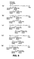
- FIG. 5 shows the variation of a calculation period of the V_on and a correction period when a voltage command value is corrected by using a value of the V_on.
- FIG. 5(a) shows an example in which correction is performed in an immediate switching half period by using the V_on which is calculated in a certain switching half period as described in the above.
- FIG. 5(b) shows an example in which correction is performed in a switching half period after the next half period using the V_on which is calculated in a certain switching half period.
- FIG. 5(c) shows an example in which correction is performed in an immediate switching one period by using the V_on which is calculated in a certain switching one period.
- FIG. 5(d) shows an example in which correction is performed in an immediate switching half period by using the V_on which is calculated in a certain switching one period.
- FIG. 5(e) shows an example in which correction is performed in an immediate switching one period by using the V_on which is calculated in a certain switching half period.
- n times-period of switching half period (n is positive integer) including switching half period, one period, one and half periods, and two periods and so forth
- m times-period of following switching half period (m is positive integer) including following switching half period, following one period, following one and half periods, and following two periods and so forth
- accuracy is not substantially decreased.
- correction may be performed in m times-period of a switching half period after the next half period or after next one period.
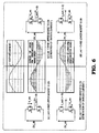
- FIG. 6 is a diagram for describing one phase of a leg comprising MOSFETs and parasitic diodes of the MOSFETs and an output current path, and a diagram of current waveform of an output current I_out and a current which flows in a semiconductor device group of each arm.
- the output current flows only in the MOSFET of an upper arm.
- the V_on is calculated not in a switching half period, but in n times-period of switching half period including switching one period and switching one and half periods, the V_on is obtained by considering each ON time ratio in n times-period of switching half period.
- a function Fvon() when the device characteristics shown in FIG. 7 are considered, by using a mathematical equation, by using a table or by using both of a mathematical equation and a table, an equivalent effect can be obtained.
- the voltage drop calculating unit 32 calculates the voltage drop V_on which is generated in a semiconductor device group by using the output current I_out which is detected, data of ON time of each switching element in a switching half period which is received from the switching control unit 33 and the function Fvon().
- the calculated voltage drop V_on is added to the voltage command V_ref1 which is generated in the voltage command generation unit 31 so as to calculate the voltage command V_ref.
- the voltage command V_ref is input to the switching control unit 33 so as to control ON/OFF of a switching element in a semiconductor device group in the next switching half period.
- a voltage drop which is generated in a MOSFET and a parasitic diode of the MOSFET can be compensated. Consequently, an output voltage with high accuracy can be obtained. Further, in a motor drive device at a low speed and with high torque, that is, the state in which an output voltage is small and current is large, a voltage drop which is generated in a semiconductor device group becomes relatively large. Therefore, when the voltage drop is not compensated, a torque ripple is generated. However, according to the present invention, the torque ripple can be decreased.
- a power converter device As described in the above, by a power converter device according to Embodiment 1 of the present invention, even in a case where a division current is generated in a semiconductor device group 25a and 25b, voltage correction with high accuracy can be performed. Further, unlike the Patent Document 1, without providing a current sensor which detects a current value and the direction of a current at an upper arm and a lower arm, respectively, by using only a current sensor 26 which detects an output current, by using a current value which is detected by the current sensor 26 and ON time ratio of switching elements which are provided at an upper arm and a lower arm, a voltage drop can be calculated, therefore the configuration of a power converter device is simple.
- FIG. 8 is a sequence diagram showing the operation of a power converter device according to Embodiment 2 of the present invention.
- Embodiment 1 a case in which a period of time when both of an upper switching element and a lower switching element are OFF-state at the same time (dead-time) is extremely small and negligible is assumed, however, in a case where there is an influence of dead-time which is provided for protecting a semiconductor device group, when a current path during dead-time and a voltage drop in a semiconductor device group are incorporated, an amount of voltage drop which is generated during dead-time can be corrected. Consequently, an output voltage with higher accuracy can be obtained.
- the dead-time Td (a period which is indicated by diagonal line) is provided by making the time-difference between rise time at power ON of a MOSFET and that at power OFF of a MOSFET for preventing short circuit so as to protect a semiconductor device group.
- a MOSFET is an OFF-state; therefore a voltage drop during the Td period is only generated in a diode. Consequently, in a case where the Td is large, an error is generated between a voltage drop which is generated during the Td period and a voltage drop correction amount which is calculated assuming that a current flows also in a MOSFET by ignoring the Td period.
- a voltage drop correction amount is obtained by considering the semiconductor device group characteristic during the Td period as shown in FIG. 9 , that is, a current does not flow in a MOSFET during the Td period.
- FIG. 9 shows the semiconductor device group characteristic during the Td period, that is, the function Fvon_td().
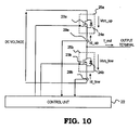
- FIG. 10 is a diagram showing a main circuit (leg) of a power converter device according to Embodiment 3 of the present invention.
- a current sensor 26 is provided so as to detect the output current I_out, however, in Embodiment 2, as shown in FIG. 10 , a current sensor 29a and a current sensor 29b are provided so as to directly detect the current Id_up which flows in a semiconductor device group of an upper arm 25a and the current Id_low which flows in a semiconductor device group of a lower arm 25b, respectively.
- the current Id_up and the current Id_low can be detected separately.
- the V_on not the output current I_out but the current Id_up and the current Id_low which are detected are used.
- a power converter device in Embodiment 3 even in a case where a division current is generated in a semiconductor device group 25a and 25b, voltage correction with high accuracy can be performed. Further, unlike the Patent Document 1, without judging whether a current flows in a switching element or in a freewheeling diode of each upper arm and each lower arm, a voltage drop can be calculated using a current value which is detected by the current sensor 29a and 29b. Consequently, the configuration of a power converter device can be simple.
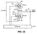
- FIG. 12 is a diagram showing a main circuit (leg) of a power converter device according to Embodiment 4 of the present invention.
- Basic configuration is same as that shown in FIG. 1 and FIG. 3 .
- a Schottky barrier diode 63a is connected in parallel as a freewheeling diode to a MOSFET 61a of a switching element of an output-side converter 2.
- a parasitic diode 62a of a MOSFET accompanies a MOSFET's structure; therefore the parasitic diode 62a also functions as a freewheeling diode.
- one set of semiconductor device group 64a comprises the MOSFET 61a, the Schottky barrier diode 63a and the parasitic diode 62a of the MOSFET.
- one set of semiconductor device group 64b comprises in the same way as that of the semiconductor device group 64a.
- a division current path has three directions. Therefore, the configuration of a control unit 22 is the same as shown in FIG. 3 , however, the following characteristic is given to the voltage drop calculating unit 32 in FIG. 3 .
- FIG. 13 shows an example of voltage drop-current characteristics of a MOSFET, a Schottky barrier diode, a parasitic diode of the MOSFET, and a semiconductor device group comprising the MOSFET, the Schottky barrier diode and the parastic diode of the MOSFET which are connected in parallel, at a certain temperature.
- a parasitic diode of the MOSFET is electrically conducted, a division current is generated in the MOSFET and the Schottky barrier diode and the parasitic diode of the MOSFET, and the characteristic, that is, an increase of a voltage drop with respect to current is further suppressed, is shown.
- the characteristic Fvon() shown in FIG. 13 is incorporated as a table, as a mathematical equation, or as both of them, and the voltage drop V_on in a semiconductor device group is output. Finally, the V_on is added so as to correct the voltage command V_ref1, and the V_ref which is final command is derived. Based on the V_ref, a switching control unit 33 performs the ON/OFF control of a switching element in a semiconductor device group.
- FIG. 13 an example in which a current flows in the order of a MOSFET, a Schottky barrier diode, and a parasitic diode of a MOSFET with respect to increase of reverse current, however, the order is not limited to the above, and there are some cases in which the order is different depending on individual characteristics.
- a MOSFET, a parasitic diode of the MOSFET and a Schottky barrier diode are used in a semiconductor device group, however, when a PiN diode is used instead of the Schottky barrier diode, by considering a PiN diode characteristic in the same way as the characteristic shown in FIG. 13 , same effect can be obtained.
- Embodiment 2 When there is an influence of dead-time, as described in Embodiment 2, by incorporating a current path and the voltage drop characteristics in a semiconductor device group, an amount of a voltage drop which is generated in dead-time can be corrected. Consequently, an output voltage with higher accuracy can be obtained in Embodiment 4.
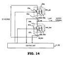
- a current sensor 65 is provided so as to detect the output current I_out, however, in the same way as the description of Embodiment 3, as shown in FIG. 14 , a current sensor 67a and a current sensor 67b may be provided so as directly detect the current Id_up which flows in a semiconductor device group 64a of an upper arm and the current Id_low which flows in a semiconductor device group 64b of a lower arm, respectively.
- a temperature sensor which detects the temperature of the semiconductor device group, or that of each semiconductor device, is attached so as to calculate a voltage drop which is generated in the semiconductor device group by using the characteristic of the semiconductor device group, that is, the function Fvon(), at the detected temperature.
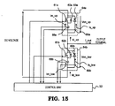
- FIG. 15 is a diagram showing a main circuit (leg) of a power converter device according to Embodiment 5 of the present invention.
- a current sensor 26 is provided so as to detect the output current I_out, or Id_up, Id_low of each upper arm or each lower arm.
- Embodiment 5 as shown in FIG.
- a current sensor 68a detects the current Im_up which flows in a semiconductor device group including the MOSFET 61a and the parasitic diode 62a of the MOSFET. Consequently, by the current which is detected by the current sensor 68a, a voltage drop which is generated in the semiconductor device group including the MOSFET 61a and the parasitic diode 62a of the MOSFET is obtained by the semiconductor device group characteristic Fvon_m() including a MOSFET and a parasitic diode indicated by a solid line in FIG. 16 .
- the current sensor 69a detects the current Is_up which flows in the Schottky barrier diode 63a. Consequently, by the current which is detected by the current sensor 69a, a voltage drop which is generated in the Schottky barrier diode 63a is obtained by the Schottky barrier diode characteristic Fvon_s() indicated by a solid line in FIG. 16 .
- a division current which flows in the Schottky barrier diode 63a is generated so as to make a voltage drop in the Schottky barrier diode 63a and a voltage drop which is generated in the semiconductor group of the MOSFET 61a and the parasitic diode 62a same.
- the current Im_up which flows in a semiconductor device group including the MOSFET 61 a and the parasitic diode 62a is I_2
- the current Is_up which flows in the Schottky barrier diode 63a is I_3, as shown by the voltage drop V_1 in FIG. 16 , both of them generate the same voltage drop V_1.
- a voltage drop in the semiconductor device group 64a of an upper arm comprising the MOSFET 61a, the parasitic diode 62a of the MOSFET and the Schottky barrier diode 63a can be obtained by Fvon_m() usuing a value of Im_up which is detected by the current sensor 68a, also can be obtained by Fvon_s() using a value of Is_up which is detected by the current sensor 69a. Values of a voltage drop which are obtained by the above-mentioned cases are same.
- FIG. 17 is a diagram showing a main circuit (leg) of a power converter device according to Embodiment 6 of the present invention.
- Basic configuration is same as that shown in FIG. 1 and FIG. 3 .
- a Schottky barrier diode 93a and a PiN diode 94a are connected in parallel as freewheeling diodes to a MOSFET 91a of a switching element of an output-side converter 2.
- one set of semiconductor device group 95a comprises the MOSFET 91a, the Schottky barrier diode 93a, the PiN diode 94a and the parasitic diode 92a of the MOSFET.
- one set of semiconductor device group 95b comprises in the same way as that of the semiconductor device group 95a.
- the performance of a parasitic diode of a MOSFET is not good, therefore, a package in which a PiN diode has been already connected is used, and in a case where a Schottky barrier diode is utilized in order to further improve the performance, the semiconductor device group having the above-mentioned configuration is often used.
- a division current path has four directions. Therefore, the configuration of a control unit 22 is the same as that in Embodiment 1, however, the following characteristic is given to a voltage drop calculating unit 32 which calculates a voltage drop in a semiconductor device group shown in FIG. 3 .
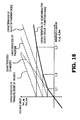
- FIG. 18 shows an example of voltage drop-current characteristics of a MOSFET, a Schottky barrier diode, PiN diode, a parasitic diode of the MOSFET, and a semiconductor device group, comprising the MOSFET, the Schottky barrier diode and the parasitic diode of the MOSFET which are connected in parallel, at a certain temperature.
- a reverse current in a semiconductor device group which is an ON-state exceeds I_1
- a Schottky barrier diode is electrically conducted, a division current is generated in the MOSFET and the Schottky barrier diode, and the characteristic, that is, an increase of a voltage drop with respect to current is suppressed, is shown.
- a reverse current in a semiconductor device group which is an ON-state exceeds I_2
- a PiN diode is electrically conducted, a division current is generated in the MOSFET, the Schottky barrier diode and the PiN diode, and the characteristic, that is, an increase of a voltage drop with respect to current is further suppressed, is shown.
- a reverse current in a semiconductor device group which is an ON-state exceeds I_3
- a parasitic diode of the MOSFET is electrically conducted, a division current is generated in the MOSFET, the Schottky barrier diode, the PiN diode and the parasitic diode of the MOSFET, and the characteristic, that is, an increase of a voltage drop with respect to current is further suppressed, is shown.
- the characteristic shown in FIG. 18 is incorporated as a table, as a mathematical equation, or as both of them, and the voltage drop V_on in a semiconductor device group is output. Finally, the V_on is added so as to correct the voltage command V_ref1, and the V_ref which is final command is derived. Based on the V_ref, a switching control unit 33 performs the ON/OFF control of a switching element in a semiconductor device group.
- FIG. 18 an example in which a current flows in the order of a MOSFET, a Schottky barrier diode, a PiN diode and a parasitic diode of a MOSFET with respect to increase of reverse current, however, the order is not limited to the above, and there are some cases in which the order is different depending on individual characteristics.
- Embodiment 6 As above-mentioned, even in a case where a Schottky barrier diode and a PiN diode are used as a freewheeling diode, according to Embodiment 6, a voltage drop which is generated in a MOSFET, a Schottky barrier diode and a parasitic diode of the MOSFET is corrected. Consequently, an output voltage with high accuracy can be obtained, and a torque ripple can be decreased.
- Embodiment 2 When there is an influence of dead-time, as described in Embodiment 2, by incorporating a current path and a voltage drop characteristics in a semiconductor device group, an amount of a voltage drop which is generated in dead-time can be corrected. Consequently, an output voltage with higher accuracy can be obtained in Embodiment 6.
- a current sensor is provided so as to detect the output current I_out, in the same way as the description of Embodiment 3.
- a current sensor 99a and a current sensor 99b may be provided so as directly detect the current Id_up which flows in a semiconductor device group 95a of an upper arm and the current Id_low which flows in a semiconductor device group 95b of a lower arm, respectively.
- accuracy can be improved by using two current sensors as shown in FIG. 19 .
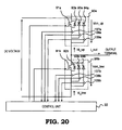
- a current sensor 107a and 107b which detect magnitudes and directions of currents which flow in a MOSFET 91a and 91b as switching elements, and parasitic diodes 92a and 92b of the MOSFET, and current sensors 108a and 108b which detect magnitudes and directions of currents of Schottky barrier diodes 93a and 93b, and current sensors 109a and 109b which detect magnitudes and directions of currents of PiN diodes 94a and 94b may be connected.
- a voltage is calculated by focusing the division characteristic of only the current which flows in a MOSFET and a parasitic diode of the MOSFET, therefore, correction accuracy can be improved.
- a temperature sensor which detects the temperature of the semiconductor device group, or that of each semiconductor device, is attached so as to calculate a voltage drop which is generated in the semiconductor device group by using the characteristic of the semiconductor device group at the detected temperature, that is, the function Fvon().
- Embodiments 1 to 6 use of a MOSFET as a switching element is assumed; however, when a JFET is used as a switching element, a division current is generated between a freewheeling diode in the same way, therefore, the effect in the same level as that of the Embodiments 1 to 6 can be obtained.
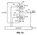
- FIG. 21 is a diagram showing a main circuit (leg) of a power converter device according to Embodiment 7 of the present invention.
- Basic configuration is same as that shown in FIG. 1 and FIG. 3 .
- an IGBT 81a is used as a switching element of an output-side converter 2
- a PiN diode 82a and a Schottky barrier diode 83a are used as freewheeling diodes
- the IGBT81a, the PiN diode 82a, the Schottky barrier diode 83a constitute a semiconductor device group 84a.
- a semiconductor device group 84b is constituted in the same way as that of the semiconductor device group 84a.
- the above-mentioned configuration is often used for the purpose such that the characteristic of a Schottky barrier diode which is more excellent than that of a PiN diode is utilized for an IGBT package in which a PiN diode is incorporated as a freewheeling diode.
- the IGBTs 8 1 a and 8 1 b which are switching elements can not make the reverse current flow; therefore a division current is not generated between a switching element and a freewheeling diode.
- a division current is generated between a PiN diode and a Schottky barrier diode which are freewheeling diodes.
- Basic configuration of a control unit 22 is the same as that shown in FIG. 3 , however, in the above-mentioned configuration of the semiconductor element group, a division path is between freewheeling diodes, therefore, following characteristic is given to a voltage drop calculating unit 32 in FIG. 3 .
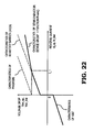
- FIG. 22 shows an example of voltage drop-current characteristics of a IGBT, a PiN diode and a Schottky barrier diode, and a semiconductor device group, comprising the IGBT, the PiN diode and the Schottky barrier diode which are connected in parallel, at a certain temperature.
- a reverse current exceeds 0 A, a current starts to flow in the Schottky barrier diode.
- the characteristic shown in FIG. 22 is incorporated as a table, as a mathematical equation, or as both of them, and the voltage drop V_on in a semiconductor device group is output. Finally, the V_on is added so as to correct the voltage command V_ref1, and the V_ref, which is final command, is derived. Based on the V_ref, ON/OFF control of a switching element in a semiconductor device group is performed.
- FIG. 22 an example in which a current flows in the order of an IGBT, a Schottky barrier diode and a PiN diode with respect to increase of reverse current.
- the order is not limited to the above, and there are some cases in which the order is different depending on individual characteristics.
- Embodiment 7 When there is an influence of dead-time, as described in Embodiment 2, by incorporating a current path and the voltage drop characteristic in a semiconductor device group, an amount of a voltage drop which is generated in dead-time can be corrected. Consequently, an output voltage with higher accuracy can be obtained in Embodiment 7.
- a current sensor 85 is provided so as to detect the output current I_out, in the same way as the description of the Embodiments, current sensors may be provided so as to directly detect the current Id_up which flows in a semiconductor device group 84a of an upper arm and the current Id_low which flows in a semiconductor device group 84b of a lower arm, respectively.
- accuracy can be improved by using two current sensors.
- a temperature sensor which detects the temperature of the semiconductor device group, or that of each semiconductor device, is attached so as to calculate a voltage drop which is generated in the semiconductor device group by using the characteristic of the semiconductor device group at the detected temperature, that is, the function Fvon().
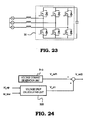
- a power converter device according to the present invention is used as an adjustable-speed motor driving device; however a power converter device according to the present invention can be used as a power converter device 20 which is connected to an electric power system as shown in FIG. 23 .
- a system current is main object to be controlled; therefore, the voltage command V_ref1 which is generated in a voltage command generation unit 310 in FIG. 24 is generated so as to control the system current.
- the voltage command generation unit 310 generates the voltage command V_ref1 so as to make an active current a suitable value.
- the V_ref1 is generated by pq control, etc.
- a voltage drop calculating unit 320 calculates a voltage drop in a semiconductor device group in the same way as that described in the Embodiments 1 to 7.
- a switching element and a diode element in the Embodiments 1 to 8 may be formed of silicon, or may be formed of a wide-band gap semiconductor whose band-gap is bigger than that of silicon.
- Wide-band gap semiconductors include silicon carbide, gallium nitride, diamond, etc.
- the switching element and the diode element which are formed of the wide-band gap semiconductors have a high withstand voltage property and a high allowable current density. Therefore, the switching element and the diode element can be miniaturized, by using the switching element and the diode element which are miniaturized, semiconductor modules in which the elements are incorporated can be miniaturized.
- the above-mentioned elements have also a high heat resistance, therefore, heat radiation fins of a heat sink can be miniaturized and a water-cooling part substituted with air cooling is possible. Consequently, further miniaturization of semiconductor modules is possible.
- both of a switching element and a diode element are formed of a wide-band gap semiconductor, however, either element may be formed of a wide-band gap semiconductor, and the effect which is described in the Embodiments 1 to 8 can be obtained.
- a PWM control is described as an example, however, a control method is as long as a method for controlling a power voltage by using the ratio of ON/OFF of a switching element, other control methods can also be applied to the present invention.
- the present invention can be applied to PDM (Pulse Density Modulation) which is a method for controlling a voltage by changing a density of a pulse having a constant width.
- PDM Pulse Density Modulation
Landscapes
- Engineering & Computer Science (AREA)
- Power Engineering (AREA)
- Inverter Devices (AREA)
- Power Conversion In General (AREA)
Abstract
Description
- This invention relates to a power converter device which converts DC power into AC power, particularly relates to an adjustable-speed motor driving device and a power converter device which is linked to a system.
- In many cases, a power converter device is configured as follows. That is, a power converter device comprises two semiconductor device groups comprising a switching element and a freewheeling diode, wherein the switching element and the freewheeling diode are connected in parallel. The two semiconductor device groups are connected in series, a DC voltage is applied to both ends of the semiconductor device groups and an output terminal is provided at a connection point between semiconductor device groups.
In the above-mentioned power converter device, when a switching element of an upper arm is an ON-state, a positive DC voltage is output to the output terminal, and when a switching element of a lower arm is an ON-state, a negative DC voltage is output to the output terminal.
Consequently, ON/OFF of a switching element is controlled so as to make an average output voltage of one switching period equal to a voltage command.
Ideally, an average output voltage of one switching period is equal to a voltage command. When an IGBT is used as a switching element, a current flows in either of a switching element or a freewheeling diode according to the direction of current. In the above-mentioned power converter device, a voltage drop (on-voltage) is generated in a switching element; therefore an output voltage according to a command value can not be obtained.
InPatent Document 1, technology to obtain an output voltage according to a command value is indicated as follows. That is, in order to compensate the voltage drop, a current sensor is provided at an upper arm and a lower arm, respectively, and a current which flows in each arm is judged whether the current flows in a switching element or in a freewheeling diode so as to compensate the each voltage drop. - On the other hand, there is a power converter device which performs a synchronous rectification in which a MOSFET is used as a switching element, and a division current between a switching element and a freewheeling diode is used so as to reduce the loss. (for example, Patent Document 2)
-
- Patent Document 1:
- National Publication of International Patent Application
WO02/084855 - Patent Document 2:
- Japanese Patent Application Laid-Open No.
2008-61403 - In a power converter device using a synchronous rectification disclosed by the
Patent Document 2, in some cases, a current is divided to flow in a switching element and in a freewheeling diode. Therefore, unlike thePatent Document 1, the voltage drop can not be compensated by judging whether the current flows in a switching element or in a freewheeling diode. - Hence, this invention aims to provide a power converter device in which a current is divided to flow in a plurality of semiconductor elements, the voltage drop in the semiconductor elements can be compensated and an output voltage with high accuracy can be obtained.
- A power converter device is disclosed which is configured such that in a leg comprising two semiconductor device groups which are connected in series, and the semiconductor device group comprises a switching element and a semiconductor device other than a switching element which are connected in parallel, a connecting point to which semiconductor device groups are connected in series is an AC output terminal, and both ends of the legs are DC terminals, and a division current is generated in a current which flows in the semiconductor device group between elements in the semiconductor device group, and a current sensor which detects a current which flows in a semiconductor device group, a voltage command generation unit which calculates a voltage command value to be output, a voltage drop calculating unit which calculates a voltage drop of a semiconductor device group by using a current value which is detected by the current sensor and a voltage drop characteristics including a division characteristic of a semiconductor device, and a switching control unit which corrects a voltage command value which is generated by the voltage command generation unit by using the voltage drop which is calculated by the voltage drop calculating unit so as to control ON/OFF of a switching element are provided.
- In a power converter device in which the current is divided to flow in a plurality of semiconductor elements, an error voltage, which is generated between a voltage command and an output voltage, and is caused by a voltage drop in a semiconductor device, is compensated and an output voltage with high accuracy can be obtained.
-
- FIG. 1
- is a circuit diagram showing an example of configuration of a power unit to which a power converter device according to
Embodiment 1 of the present invention is applied; - FIG. 2
- is a circuit diagram showing a main circuit (leg) of a power converter device according to
Embodiment 1 of the present invention; - FIG. 3
- is a block diagram showing a control unit of a power converter device according to
Embodiment 1 of the present invention; - FIG. 4
- is a sequence diagram showing the operation of a power converter device according to
Embodiment 1 of the present invention; - FIG. 5
- is a diagram explaining the variation of a calculation period of V_on and a correction period in which a voltage command value is corrected by using the value of V_on according to
Embodiment 1 of the present invention; - FIG. 6
- is a diagram explaining the operation of each state of a power converter device according to
Embodiment 1 of the present invention; - FIG. 7
- is a diagram showing voltage-drop characteristics including a division current characteristic of semiconductor device group according to
Embodiment 1 of the present invention; - FIG. 8
- is a sequence diagram explaining the operation of a power converter device according to
Embodiment 2 of the present invention; - FIG. 9
- is a diagram showing an example of voltage-drop characteristics including a division current characteristic of semiconductor device group in dead time according to
Embodiment 2 of the present invention; - FIG. 10
- is a circuit diagram showing a main circuit (leg) of a power converter device according to Embodiment 3 of the present invention;
- FIG. 11
- is a block diagram showing a control unit of a power converter device according to Embodiment 3 of the present invention;
- FIG. 12
- is a circuit diagram showing a main circuit (leg) of a power converter device according to Embodiment 4 of the present invention;
- FIG. 13
- is a diagram showing an example of voltage-drop characteristics including a division characteristic of semiconductor device group according to Embodiment 4 of the present invention;
- FIG. 14
- is a circuit diagram showing a main circuit (leg) of another power converter device according to Embodiment 4 of the present invention;
- FIG. 15
- is a circuit diagram showing a main circuit (leg) of a power converter device according to Embodiment 5 of the present invention;
- FIG. 16
- is a diagram showing an example of voltage-drop characteristics including a division current characteristic of semiconductor device group according to Embodiment 5 of the present invention;
- FIG. 17
- is a circuit diagram showing a main circuit (leg) of a power converter device according to Embodiment 6 of the present invention;
- FIG. 18
- is a diagram showing an example of voltage-drop characteristics including a division current characteristic of semiconductor device group according to Embodiment 6 of the present invention;
- FIG. 19
- is a circuit diagram showing a main circuit (leg) of another power converter device according to Embodiment 6 of the present invention;
- FIG. 20
- is a circuit diagram showing a main circuit (leg) of another power converter device according to Embodiment 6 of the present invention;
- FIG. 21
- is a circuit diagram showing a main circuit (leg) of a power converter device according to Embodiment 7 of the present invention;
- FIG. 22
- is a diagram showing an example of voltage-drop characteristics including a division current characteristic of semiconductor device group according to Embodiment 7 of the present invention;
- FIG. 23
- is a circuit diagram showing another example of configuration of a power unit to which a power converter device according to the present invention is applied; and
- FIG. 24
- is a block diagram showing a control unit in a case where a power converter device of the present invention is applied to a power unit shown in
FIG. 23 . -
FIG. 1 is a diagram showing a circuit of a power unit to which the present invention is applied.FIG. 1 is a circuit diagram in a case where a power converter device of the present invention is applied to an adjustable-speed motor driving device as an example of a power unit. The power unit is divided broadly into an input-side converter 1 and an output-side converter 2, and both of the input-side converter 1 and the output-side converter 2 are commonly connected to aDC section 10. The input-side converter 1 mainly comprises a diode rectifier 3 and an AC reactor 4, and is connected to an electric power system 5. The diode rectifier 3 comprises PiN diodes, whose rated voltage is higher than a DC voltage, or of Schottky barrier diodes, and the diode rectifier 3 converts an AC system voltage to a DC voltage. - On the other hand, as the output-
side converter 2, a semiconductor group comprising a switching element and a freewheeling diode, which is a semiconductor element other than the switching element, which are connected in parallel, is used, and more than oneleg 21, which is the semiconductor device groups are connected in series, is used depending on necessary number of phases of output.
Both ends of eachleg 21 are connected to theDC section 10 in common, at a middle point of theleg 21, that is, at a connection point of a semiconductor device group, an AC output terminal which is connected to a motor 8 is provided.
In a case of three-phase motor driving, threelegs 21 are used, in total; six semiconductor device groups are used. Further, acontrol unit 22 which controls the motor 8 is provided, and thecontrol unit 22 finally controls ON/OFF of switching elements in semiconductor device groups. Further, in the present invention, the output-side converter 2 is a power converter device which is an object of the invention. -
FIG. 2 is a diagram in which one phase portion ofleg 21 is focused, and describing the details of the output-side converter 2. The output-side converter 2 comprises amain circuit unit 21 which is a leg and thecontrol unit 22. In themain circuit unit 21, when an upper arm is explained as an example, one set ofsemiconductor device group 25a comprises aswitching element 23a and afreewheeling diode 24a, and theswitching element 23a and thefreewheeling diode 24a are connected in parallel.
InEmbodiment 1, the switchingelement 23a is one or more MOSFETs, and thefreewheeling diode 24a is a parasitic diode of the MOSFET. Therefore, thesemiconductor device group 25a comprises theMOSFET 23a and the parasitic diode of theMOSFET 24a.FIG. 2 shows an example having only one MOSFET, however in a case where the amount of current is large, a plurality of MOSFETs may be connected in parallel, in a case where a voltage is high, a plurality of MOSFETs may be connected in series, and both of them may be used concurrently.
Asemiconductor device group 25b is configured in the same way as that of thesemiconductor device group 25a.Reference numeral 26 indicates a current sensor and is used for detecting the direction and an amount of an output current, for example, a current sensor in which a hole sensor, etc. is used can be used. - On the other hand, the final objective of the
control unit 22 is to control a torque or a number of rotations, etc of a motor which is connected to an output terminal. In order to perform the final objective, thecontrol unit 22 controls ON/OFF of theswitching element - In order to describe the
control unit 22 in more detail, inFIG. 3 , a block diagram of thecontrol unit 22 is shown. Thecontrol unit 22 mainly comprises a voltagecommand generation unit 31 which calculates a voltage command value for controlling the speed of a motor and the torque, a voltagedrop calculating unit 32 which calculates a voltage drop of a semiconductor device group and aswitching control unit 33. The voltagecommand generation unit 31 can easily generate the voltage command V_ref1 by using well-know technology including a vector control and a V/f constant control which have been commonly used.
For example, in a case where a motor having a rated speed of 1,800 rpm, a rated frequency of 60 Hz and a rated voltage (line voltage) of 200 V is driven, when the motor is controlled to be 900 rpm, which is the half of the rated speed, by using a V/f constant control, at 30 Hz, a voltage, which is made by phase voltage converting 100 V, which is half of the rated voltage, is given as the voltage command V_ref1. - In the
switching control unit 33, ON/OFF of a switching element is determined so as to make the voltage command V_ref1 which is given coincides with an average voltage of an output voltage in a switching half period. Generally, in many cases, PWM control is performed as a control, in a case of PWM control, a method in which a space vector is used, or a triangular wave carrier comparison method is used, here, a triangular wave carrier comparison method as shown inFIG. 4 is described as an example. - A middle point of a DC section is conceived as a reference potential of a virtual phase voltage, and a DC voltage is set as ±VDC (a voltage between both ends of a leg is 2 Vdc). Maximum value and minimum value of a triangular wave carrier shown in
FIG. 4 is +1, and - 1 , respectively. Standardization is performed by dividing the voltage command V_ref which is given to the switchingcontrol unit 33 by VDC so as to calculate the command value signal V_ref/Vdc.
The command value signal V_ref/VDC which is standardized and a triangular wave carrier are compared, when the command value signal is larger than the triangular wave carrier, a switching element of an upper arm is an ON-state and a switching element of a lower arm is an OFF-state. In reverse, when the command value signal is smaller than the triangular wave carrier, a switching element of an upper arm is an OFF-state and a switching element of a lower arm is an ON-state. By performing the control as above-mentioned, ideally, the output voltage average value V_out in a switching half period Tsw equals to the voltage command V_ref. - However, in the voltage
command generation unit 31, the voltage command value V_ref1 is determined without regard for a voltage drop which is generated in a semiconductor device group. Therefore, in a case where the switchingcontrol unit 33 determines the ON/OFF time of a switching element by using the V_ref1, the actual output voltage V_out is obtained by reducing an amount of the voltage drop V_on in a semiconductor device group from the voltage command V_ref1, that is, V_out = V_ref1 - V_on. - Then, the voltage drop V_on in a semiconductor device group which is generated in a certain switching half period is corrected at the next switching half period, and the V_ref is given as the V_ref1 + V_on to the switching
control unit 33. The voltagedrop calculating unit 32 calculates the V_on. Further, the frequency of a triangular wave carrier is, for example, 10 kHz, that is, a switching period is 100 µs, and a switching half period which is indicated by Tsw inFIG. 4 is 50 µs.
Consequently, in a case where performing calculation is not in time, even if correction is performed in the next switching half period after the next or further in the next switching half period, the accuracy is not substantially decreased. - Further, here, the voltage drop V_on of a semiconductor device group which is generated in a certain switching half period is corrected in the next, or the next after the next switching half period, however, it is not always necessary to perform calculation and correction of a voltage drop in the half period unit, but it may perform calculation and correction of a voltage drop in the integer multiple unit of the half period.
FIG. 5 shows the variation of a calculation period of the V_on and a correction period when a voltage command value is corrected by using a value of the V_on.
FIG. 5(a) shows an example in which correction is performed in an immediate switching half period by using the V_on which is calculated in a certain switching half period as described in the above.
FIG. 5(b) shows an example in which correction is performed in a switching half period after the next half period using the V_on which is calculated in a certain switching half period.
FIG. 5(c) shows an example in which correction is performed in an immediate switching one period by using the V_on which is calculated in a certain switching one period.
FIG. 5(d) shows an example in which correction is performed in an immediate switching half period by using the V_on which is calculated in a certain switching one period.FIG. 5(e) shows an example in which correction is performed in an immediate switching one period by using the V_on which is calculated in a certain switching half period. - That is, when an on-voltage in n times-period of switching half period (n is positive integer) including switching half period, one period, one and half periods, and two periods and so forth is corrected in m times-period of following switching half period (m is positive integer) including following switching half period, following one period, following one and half periods, and following two periods and so forth, accuracy is not substantially decreased. In a case where performing calculation is not in time, correction is not required to perform in an immediate m times-period of switching half period, correction may be performed in m times-period of a switching half period after the next half period or after next one period.
-
FIG. 6 is a diagram for describing one phase of a leg comprising MOSFETs and parasitic diodes of the MOSFETs and an output current path, and a diagram of current waveform of an output current I_out and a current which flows in a semiconductor device group of each arm. InFIG. 6 , for example, in a case where an output current is positive and a MOSFET of an upper arm is an ON-state, (the state shown in (a)), the output current flows only in the MOSFET of an upper arm.
On the other hand, in a case where an output current is positive and a MOSFET of a lower arm is an ON-state, (the state shown in (b)), the output current flows in the MOSFET of a lower arm, and a freewheeling diode which is parallel- connected to the MOSFET of a lower arm (so called, division current). In a case where an output current is negative, the state is reverse. (the state shown in (c) or (d)).
Further, as shown inFIG. 6 , current waveform of each semiconductor device group is waveform in which a current alternately flows in an upper element group and a lower element group. The voltage drop V_on which is generated in a semiconductor device group depends on division current characteristics. The voltagedrop calculating unit 32 shown inFIG. 3 calculates above mentioned voltage drop which is generated in the semiconductor device group. -
FIG. 7 shows an example of voltage drop-current characteristics (thick solid line = function Fvon()) of a MOSFET, a parasitic diode of the MOSFET, and of a semiconductor device group comprising the MOSFET and the parasitic diode of the MOSFET which are connected in parallel, at a certain temperature. InFIG. 7 , in a case where a reverse current in a semiconductor device group which is an ON-state ( = Id_up or Id_low ) is I_1 or lower, a current flows only in a MOSFET, therefore a linear characteristic is shown.
On the other hand, in a case where a reverse current in a semiconductor device group which is an ON-state exceeds I_1, a parasitic diode of the MOSFET is electrically conducted, a division current is generated in the MOSFET and the parasitic diode of the MOSFET, the characteristic, that is, an increase of a voltage drop with respect to current is suppressed, is shown. - That is, in a period of time while a switching element of an upper arm is an ON-state, (= Ton_up refer to
FIG. 4 ), the reverse current Id_up in a semiconductor device group of an upper arm is -I_out, the voltage drop Von_up in a switching element of the upper arm is obtained by Fvon(-I_out).
On the other hand, in a period of time while a switching element of a lower arm is an ON-state, (= Ton_low, refer toFIG. 4 ) the reverse current Id_low in a semiconductor device group of the lower arm is +I_out, the voltage drop Von_low in a semiconductor device group of the lower arm is obtained by Fvon(I_out). In consideration of ON time ratio in a switching half period (= Tsw), an average value of the voltage drop V_on which is generated in a switching half period is obtained by the Equation (1).
- Further, in a case where the V_on is calculated not in a switching half period, but in n times-period of switching half period including switching one period and switching one and half periods, the V_on is obtained by considering each ON time ratio in n times-period of switching half period.
- Further, regarding a function Fvon(), when the device characteristics shown in
FIG. 7 are considered, by using a mathematical equation, by using a table or by using both of a mathematical equation and a table, an equivalent effect can be obtained. For example, the function Fvon() is obtained according to the condition of reverse current Id as follows. That is,
and
Constant A, B and C are determined corresponding a semiconductor device to be used. - As above-mentioned, the voltage
drop calculating unit 32 calculates the voltage drop V_on which is generated in a semiconductor device group by using the output current I_out which is detected, data of ON time of each switching element in a switching half period which is received from the switchingcontrol unit 33 and the function Fvon().
The calculated voltage drop V_on is added to the voltage command V_ref1 which is generated in the voltagecommand generation unit 31 so as to calculate the voltage command V_ref. The voltage command V_ref is input to the switchingcontrol unit 33 so as to control ON/OFF of a switching element in a semiconductor device group in the next switching half period. - By performing the above-mentioned, a voltage drop which is generated in a MOSFET and a parasitic diode of the MOSFET can be compensated. Consequently, an output voltage with high accuracy can be obtained. Further, in a motor drive device at a low speed and with high torque, that is, the state in which an output voltage is small and current is large, a voltage drop which is generated in a semiconductor device group becomes relatively large. Therefore, when the voltage drop is not compensated, a torque ripple is generated. However, according to the present invention, the torque ripple can be decreased.
- Further, in the above-mentioned description, use of a semiconductor device at a certain constant temperature is assumed, however, the characteristic of a semiconductor device changes according to temperatures. Therefore, under the conditions where temperatures of a semiconductor device change intensely, a temperature sensor which detects the temperature of the semiconductor device group, or that of each semiconductor device, is attached so as to calculate a voltage drop which is generated in the semiconductor device group by using a characteristic, that is, the function Fvon(), of the semiconductor device group at the detected temperature. By performing the above-mentioned, the accuracy is further improved.
- As described in the above, by a power converter device according to
Embodiment 1 of the present invention, even in a case where a division current is generated in asemiconductor device group Patent Document 1, without providing a current sensor which detects a current value and the direction of a current at an upper arm and a lower arm, respectively, by using only acurrent sensor 26 which detects an output current, by using a current value which is detected by thecurrent sensor 26 and ON time ratio of switching elements which are provided at an upper arm and a lower arm, a voltage drop can be calculated, therefore the configuration of a power converter device is simple. -
FIG. 8 is a sequence diagram showing the operation of a power converter device according toEmbodiment 2 of the present invention. InEmbodiment 1, a case in which a period of time when both of an upper switching element and a lower switching element are OFF-state at the same time (dead-time) is extremely small and negligible is assumed, however, in a case where there is an influence of dead-time which is provided for protecting a semiconductor device group, when a current path during dead-time and a voltage drop in a semiconductor device group are incorporated, an amount of voltage drop which is generated during dead-time can be corrected. Consequently, an output voltage with higher accuracy can be obtained. - As shown in
FIG. 8 , the dead-time Td (a period which is indicated by diagonal line) is provided by making the time-difference between rise time at power ON of a MOSFET and that at power OFF of a MOSFET for preventing short circuit so as to protect a semiconductor device group.
During the Td period, a MOSFET is an OFF-state; therefore a voltage drop during the Td period is only generated in a diode. Consequently, in a case where the Td is large, an error is generated between a voltage drop which is generated during the Td period and a voltage drop correction amount which is calculated assuming that a current flows also in a MOSFET by ignoring the Td period. In this case, a voltage drop correction amount is obtained by considering the semiconductor device group characteristic during the Td period as shown inFIG. 9 , that is, a current does not flow in a MOSFET during the Td period. - Concretely, a correction amount of a voltage drop is obtained as follows.
FIG. 9 shows the semiconductor device group characteristic during the Td period, that is, the function Fvon_td(). When a current I_out is positive, the current flows in a diode of a lower arm and when the current I_out is negative, the current flows in a diode of an upper arm.
Further in a case where more than two diodes are connected in parallel, such as a case where a Schottky barrier diode in addition to a parasitic diode of the MOSFET are connected in parallel, which will be described in Embodiment 4 later, for example, when an output current is I_1 or lower, a current only flows in the Schottky barrier diode, when an output current is I_1 or higher, a current also flows in the parasitic diode of the MOSFET, therefore a division current is generated.
The characteristic in which the above-mentioned is considered is the characteristic of a semiconductor device group Fvon_td() during the Td period shown inFIG. 9 . Then, by using the function Fvon_td() and the semiconductor device group characteristic Fvon() in a period other than the Td period, an average value of a voltage drop in a switching half period is obtained by the Equation (5).
Consequently, as above-mentioned, a correction amount of the V_on can be obtained. -
FIG. 10 is a diagram showing a main circuit (leg) of a power converter device according to Embodiment 3 of the present invention. InEmbodiment 1, acurrent sensor 26 is provided so as to detect the output current I_out, however, inEmbodiment 2, as shown inFIG. 10 , acurrent sensor 29a and acurrent sensor 29b are provided so as to directly detect the current Id_up which flows in a semiconductor device group of anupper arm 25a and the current Id_low which flows in a semiconductor device group of alower arm 25b, respectively.
Generally, when the output current is I_out = - Id_up + Id_low, either the Id_up or the Id_low is zero depending on the switching state, however, in a case where a leakage current when a MOSFET is in an OFF-state is not be negligible, accuracy can be improved by using thecurrent sensor FIG. 10 . - In this case, as a current value of a current which flows in an upper arm and a lower arm, the current Id_up and the current Id_low can be detected separately. Here, in order to obtain the V_on, not the output current I_out but the current Id_up and the current Id_low which are detected are used. The detected current Id_up and Id_low are current values which are weighted according to respective ON-time ratio. Therefore, unlike the Equation (1), it is not necessary to use respective ON-time ratio, by using Equation (4)

an average value of the V_on can be obtained. Consequently, in a voltagedrop calculating unit 32 in acontrol unit 22 in Embodiment 3, as shown inFIG. 11 , it is not necessary to receive the data regarding ON-time from a switchingcontrol unit 33. - As above described, according to a power converter device in Embodiment 3, even in a case where a division current is generated in a
semiconductor device group
Further, unlike thePatent Document 1, without judging whether a current flows in a switching element or in a freewheeling diode of each upper arm and each lower arm, a voltage drop can be calculated using a current value which is detected by thecurrent sensor -
FIG. 12 is a diagram showing a main circuit (leg) of a power converter device according to Embodiment 4 of the present invention. Basic configuration is same as that shown inFIG. 1 andFIG. 3 . In Embodiment 4, unlikeFIG. 2 inEmbodiment 1, as shown inFIG. 12 , when an upper arm is taken as an example, aSchottky barrier diode 63a is connected in parallel as a freewheeling diode to aMOSFET 61a of a switching element of an output-side converter 2.
Also in this case, aparasitic diode 62a of a MOSFET accompanies a MOSFET's structure; therefore theparasitic diode 62a also functions as a freewheeling diode. Consequently, one set ofsemiconductor device group 64a comprises theMOSFET 61a, theSchottky barrier diode 63a and theparasitic diode 62a of the MOSFET. In a lower arm, one set ofsemiconductor device group 64b comprises in the same way as that of thesemiconductor device group 64a.
According to the above-mentioned configuration of a semiconductor device group, the performance of a parasitic diode of a MOSFET is not good; therefore, the semiconductor device group having the above-mentioned configuration is often used for the purpose of utilizing the performance of a Schottky barrier diode as a freewheeling diode. - In the above-mentioned configuration of a semiconductor device group, a division current path has three directions. Therefore, the configuration of a
control unit 22 is the same as shown inFIG. 3 , however, the following characteristic is given to the voltagedrop calculating unit 32 inFIG. 3 . -
FIG. 13 shows an example of voltage drop-current characteristics of a MOSFET, a Schottky barrier diode, a parasitic diode of the MOSFET, and a semiconductor device group comprising the MOSFET, the Schottky barrier diode and the parastic diode of the MOSFET which are connected in parallel, at a certain temperature. InFIG. 13 , in a case where a reverse current in a semiconductor device group which is an ON-state (= Id_up or Id_low) is I_1 or lower, a current flows only in a MOSFET, therefore a linear characteristic is shown.
On the other hand, in a case where a reverse current in a semiconductor device group which is an ON-state exceeds I_1, a Schottky barrier diode is electrically conducted, a division current is generated in the MOSFET and the Schottky barrier, and the characteristic, that is, an increase of a voltage drop with respect to a current is suppressed, is shown.
Further, in a case where a reverse current in a semiconductor device group which is an ON-state exceeds I_2, a parasitic diode of the MOSFET is electrically conducted, a division current is generated in the MOSFET and the Schottky barrier diode and the parasitic diode of the MOSFET, and the characteristic, that is, an increase of a voltage drop with respect to current is further suppressed, is shown. - In the voltage
drop calculating unit 32 inFIG. 3 which calculates a voltage drop in a semiconductor device group, the characteristic Fvon() shown inFIG. 13 is incorporated as a table, as a mathematical equation, or as both of them, and the voltage drop V_on in a semiconductor device group is output. Finally, the V_on is added so as to correct the voltage command V_ref1, and the V_ref which is final command is derived. Based on the V_ref, a switchingcontrol unit 33 performs the ON/OFF control of a switching element in a semiconductor device group. - In
FIG. 13 , an example in which a current flows in the order of a MOSFET, a Schottky barrier diode, and a parasitic diode of a MOSFET with respect to increase of reverse current, however, the order is not limited to the above, and there are some cases in which the order is different depending on individual characteristics. - As above-mentioned, even in a case where a Schottky barrier diode is used as a freewheeling diode, according to Embodiment 4, a voltage drop which is generated in a MOSFET, a Schottky barrier diode and a parasitic diode of the MOSFET is corrected. Consequently, an output voltage with high accuracy can be obtained, and a torque ripple can be decreased.
- In the above description, a MOSFET, a parasitic diode of the MOSFET and a Schottky barrier diode are used in a semiconductor device group, however, when a PiN diode is used instead of the Schottky barrier diode, by considering a PiN diode characteristic in the same way as the characteristic shown in
FIG. 13 , same effect can be obtained. - When there is an influence of dead-time, as described in
Embodiment 2, by incorporating a current path and the voltage drop characteristics in a semiconductor device group, an amount of a voltage drop which is generated in dead-time can be corrected. Consequently, an output voltage with higher accuracy can be obtained in Embodiment 4. - In the above-mentioned, a
current sensor 65 is provided so as to detect the output current I_out, however, in the same way as the description of Embodiment 3, as shown inFIG. 14 , acurrent sensor 67a and acurrent sensor 67b may be provided so as directly detect the current Id_up which flows in asemiconductor device group 64a of an upper arm and the current Id_low which flows in asemiconductor device group 64b of a lower arm, respectively.
Generally, when the output current is I_out = - Id_up + Id_low, either the Id_up or the Id_low is zero depending on the switching state, however, in a case where a leakage current when a MOSFET is an OFF-state is not be negligible, accuracy can be improved by using thecurrent sensor FIG. 14 . - Further, in the same way as that described in
Embodiment 1, under the conditions where temperatures of a semiconductor device change intensely, a temperature sensor which detects the temperature of the semiconductor device group, or that of each semiconductor device, is attached so as to calculate a voltage drop which is generated in the semiconductor device group by using the characteristic of the semiconductor device group, that is, the function Fvon(), at the detected temperature. By performing the above-mentioned, the accuracy is further improved. -
FIG. 15 is a diagram showing a main circuit (leg) of a power converter device according to Embodiment 5 of the present invention. In Embodiment 4, acurrent sensor 26 is provided so as to detect the output current I_out, or Id_up, Id_low of each upper arm or each lower arm.
However, in Embodiment 5, as shown inFIG. 15 , in order to directly detect a current which flows in each semiconductor device including MOSFETs constituting asemiconductor device group current sensors MOSFETs 61 a and 6 1 b which are switching elements, and aparasitic diode current sensor Schottky barrier diodes - Calculation of correction value of a voltage drop in this case is described referring
FIG. 16 . An upper arm is focused. Acurrent sensor 68a detects the current Im_up which flows in a semiconductor device group including theMOSFET 61a and theparasitic diode 62a of the MOSFET. Consequently, by the current which is detected by thecurrent sensor 68a, a voltage drop which is generated in the semiconductor device group including theMOSFET 61a and theparasitic diode 62a of the MOSFET is obtained by the semiconductor device group characteristic Fvon_m() including a MOSFET and a parasitic diode indicated by a solid line inFIG. 16 .
Further, thecurrent sensor 69a detects the current Is_up which flows in theSchottky barrier diode 63a. Consequently, by the current which is detected by thecurrent sensor 69a, a voltage drop which is generated in theSchottky barrier diode 63a is obtained by the Schottky barrier diode characteristic Fvon_s() indicated by a solid line inFIG. 16 . - As can be seen in
FIG. 16 , when the total current Id_up of an upper arm is I_1 or lower, a division current which flows in theSchottky barrier diode 63a is not generated, and the current which is detected by thecurrent sensor 69a is zero. At this time, Im_up is I_1 or lower, and the voltage drop Von_up is obtained by a value of the current Im_up which is detected by thecurrent sensor 68a and Fvon_m() shown inFIG. 16 . When Id_up is I_1 or higher, a division current which flows in theSchottky barrier diode 63a is generated.
At this time, a division current which flows in theSchottky barrier diode 63a is generated so as to make a voltage drop in theSchottky barrier diode 63a and a voltage drop which is generated in the semiconductor group of theMOSFET 61a and theparasitic diode 62a same.
When the current Im_up which flows in a semiconductor device group including theMOSFET 61 a and theparasitic diode 62a is I_2, and the current Is_up which flows in theSchottky barrier diode 63a is I_3, as shown by the voltage drop V_1 inFIG. 16 , both of them generate the same voltage drop V_1. As above-mentioned, a division current is generated in such a way that Id_up = I_2 + I_3.
At this time, a voltage drop in thesemiconductor device group 64a of an upper arm comprising theMOSFET 61a, theparasitic diode 62a of the MOSFET and theSchottky barrier diode 63a can be obtained by Fvon_m() usuing a value of Im_up which is detected by thecurrent sensor 68a, also can be obtained by Fvon_s() using a value of Is_up which is detected by thecurrent sensor 69a. Values of a voltage drop which are obtained by the above-mentioned cases are same. - For example, in a case where the characteristic of a parasitic diode of a MOSFET can not be accurately expressed by a function or a table, when the current is I_1 or lower, the function Fvon_m() of a MOSFET characteristic is adopted, and when the current is I_1 or higher, the function Fvon_s() of a Schottky barrier diode is adopted. By performing the above, ON voltage can be corrected with higher accuracy than the case which is described in Embodiment 4.
-
FIG. 17 is a diagram showing a main circuit (leg) of a power converter device according to Embodiment 6 of the present invention. Basic configuration is same as that shown inFIG. 1 andFIG. 3 . In Embodiment 6, unlikeFIG. 2 inEmbodiment 1, as shown inFIG. 17 , when an upper arm is taken as an example, aSchottky barrier diode 93a and aPiN diode 94a are connected in parallel as freewheeling diodes to aMOSFET 91a of a switching element of an output-side converter 2.
Also in this case, aparasitic diode 92a of the MOSFET accompanies a MOSFET's structure; therefore theparasitic diode 92a also functions as a freewheeling diode. Consequently, one set ofsemiconductor device group 95a comprises theMOSFET 91a, theSchottky barrier diode 93a, thePiN diode 94a and theparasitic diode 92a of the MOSFET. In a lower arm, one set ofsemiconductor device group 95b comprises in the same way as that of thesemiconductor device group 95a. - According to the above-mentioned configuration of a semiconductor device group, the performance of a parasitic diode of a MOSFET is not good, therefore, a package in which a PiN diode has been already connected is used, and in a case where a Schottky barrier diode is utilized in order to further improve the performance, the semiconductor device group having the above-mentioned configuration is often used.
In the above-mentioned configuration of a semiconductor device group, a division current path has four directions. Therefore, the configuration of acontrol unit 22 is the same as that inEmbodiment 1, however, the following characteristic is given to a voltagedrop calculating unit 32 which calculates a voltage drop in a semiconductor device group shown inFIG. 3 . -
FIG. 18 shows an example of voltage drop-current characteristics of a MOSFET, a Schottky barrier diode, PiN diode, a parasitic diode of the MOSFET, and a semiconductor device group, comprising the MOSFET, the Schottky barrier diode and the parasitic diode of the MOSFET which are connected in parallel, at a certain temperature.
InFIG. 18 , in a case where a reverse current in a semiconductor device group which is an ON-state ((= Id_up or Id_low) is I_1 or lower, a current flows only in a MOSFET, therefore a linear characteristic is shown.
On the other hand, in a case where a reverse current in a semiconductor device group which is an ON-state exceeds I_1, a Schottky barrier diode is electrically conducted, a division current is generated in the MOSFET and the Schottky barrier diode, and the characteristic, that is, an increase of a voltage drop with respect to current is suppressed, is shown.
Further, in a case where a reverse current in a semiconductor device group which is an ON-state exceeds I_2, a PiN diode is electrically conducted, a division current is generated in the MOSFET, the Schottky barrier diode and the PiN diode, and the characteristic, that is, an increase of a voltage drop with respect to current is further suppressed, is shown.
Further, in a case where a reverse current in a semiconductor device group which is an ON-state exceeds I_3, a parasitic diode of the MOSFET is electrically conducted, a division current is generated in the MOSFET, the Schottky barrier diode, the PiN diode and the parasitic diode of the MOSFET, and the characteristic, that is, an increase of a voltage drop with respect to current is further suppressed, is shown. - In the voltage
drop calculating unit 32 inFIG. 3 , the characteristic shown inFIG. 18 is incorporated as a table, as a mathematical equation, or as both of them, and the voltage drop V_on in a semiconductor device group is output. Finally, the V_on is added so as to correct the voltage command V_ref1, and the V_ref which is final command is derived. Based on the V_ref, a switchingcontrol unit 33 performs the ON/OFF control of a switching element in a semiconductor device group. - In
FIG. 18 , an example in which a current flows in the order of a MOSFET, a Schottky barrier diode, a PiN diode and a parasitic diode of a MOSFET with respect to increase of reverse current, however, the order is not limited to the above, and there are some cases in which the order is different depending on individual characteristics. - As above-mentioned, even in a case where a Schottky barrier diode and a PiN diode are used as a freewheeling diode, according to Embodiment 6, a voltage drop which is generated in a MOSFET, a Schottky barrier diode and a parasitic diode of the MOSFET is corrected. Consequently, an output voltage with high accuracy can be obtained, and a torque ripple can be decreased.
- When there is an influence of dead-time, as described in
Embodiment 2, by incorporating a current path and a voltage drop characteristics in a semiconductor device group, an amount of a voltage drop which is generated in dead-time can be corrected. Consequently, an output voltage with higher accuracy can be obtained in Embodiment 6. - In the above-mentioned, a current sensor is provided so as to detect the output current I_out, in the same way as the description of Embodiment 3. However, as shown in
FIG. 19 , acurrent sensor 99a and acurrent sensor 99b may be provided so as directly detect the current Id_up which flows in asemiconductor device group 95a of an upper arm and the current Id_low which flows in asemiconductor device group 95b of a lower arm, respectively.
Generally, the output current is I_out = - Id_up + Id_low and either the Id_up or the Id_low is zero. However, in a case where a leakage current when a MOSFET is an OFF-state is not be negligible, accuracy can be improved by using two current sensors as shown inFIG. 19 . - Further, in the same way as that described in Embodiment 5, as shown in
FIG. 20 , in order to directly detect a current which flows in each semiconductor device including a MOSFET and a freewheeling diode constituting a semiconductor device group, acurrent sensor MOSFET parasitic diodes current sensors Schottky barrier diodes current sensors PiN diodes
In this case, when a voltage is calculated by focusing the division characteristic of only the current which flows in a MOSFET and a parasitic diode of the MOSFET, therefore, correction accuracy can be improved. - Further, in the same way as that described in
Embodiment 1, under the conditions where temperatures of a semiconductor device change intensely, a temperature sensor which detects the temperature of the semiconductor device group, or that of each semiconductor device, is attached so as to calculate a voltage drop which is generated in the semiconductor device group by using the characteristic of the semiconductor device group at the detected temperature, that is, the function Fvon(). By performing the above-mentioned, the accuracy is further improved. - Further, in the
Embodiments 1 to 6, use of a MOSFET as a switching element is assumed; however, when a JFET is used as a switching element, a division current is generated between a freewheeling diode in the same way, therefore, the effect in the same level as that of theEmbodiments 1 to 6 can be obtained. -
FIG. 21 is a diagram showing a main circuit (leg) of a power converter device according to Embodiment 7 of the present invention. Basic configuration is same as that shown inFIG. 1 andFIG. 3 . In Embodiment 7, as shown inFIG. 21 , when an upper arm is taken as an example, anIGBT 81a is used as a switching element of an output-side converter 2, aPiN diode 82a and aSchottky barrier diode 83a are used as freewheeling diodes, and the IGBT81a, thePiN diode 82a, theSchottky barrier diode 83a constitute asemiconductor device group 84a.
In a lower arm, asemiconductor device group 84b is constituted in the same way as that of thesemiconductor device group 84a. The above-mentioned configuration is often used for the purpose such that the characteristic of a Schottky barrier diode which is more excellent than that of a PiN diode is utilized for an IGBT package in which a PiN diode is incorporated as a freewheeling diode. - In the above-mentioned configuration, the IGBTs 8 1 a and 8 1 b which are switching elements can not make the reverse current flow; therefore a division current is not generated between a switching element and a freewheeling diode. However, a division current is generated between a PiN diode and a Schottky barrier diode which are freewheeling diodes.
Basic configuration of acontrol unit 22 is the same as that shown inFIG. 3 , however, in the above-mentioned configuration of the semiconductor element group, a division path is between freewheeling diodes, therefore, following characteristic is given to a voltagedrop calculating unit 32 inFIG. 3 . -
FIG. 22 shows an example of voltage drop-current characteristics of a IGBT, a PiN diode and a Schottky barrier diode, and a semiconductor device group, comprising the IGBT, the PiN diode and the Schottky barrier diode which are connected in parallel, at a certain temperature. InFIG. 22 , in a case where a reverse current in a semiconductor device group which is an ON-state ((= Id_up or Id_low) is 0 A or lower, a current flows only in the IGBT.
On the other hand, in a case where a reverse current exceeds 0 A, a current starts to flow in the Schottky barrier diode. Next, when a reverse current exceeds I_1, a current also starts to flow in the PiN diode, a division current is generated between the Schottky barrier diode and the PiN diode, and the characteristic, that is, an increase of a voltage drop with respect to current is further suppressed, is shown. - In the voltage
drop calculating unit 32 inFIG. 3 , the characteristic shown inFIG. 22 is incorporated as a table, as a mathematical equation, or as both of them, and the voltage drop V_on in a semiconductor device group is output. Finally, the V_on is added so as to correct the voltage command V_ref1, and the V_ref, which is final command, is derived. Based on the V_ref, ON/OFF control of a switching element in a semiconductor device group is performed. - In
FIG. 22 , an example in which a current flows in the order of an IGBT, a Schottky barrier diode and a PiN diode with respect to increase of reverse current. However, the order is not limited to the above, and there are some cases in which the order is different depending on individual characteristics. - ] As above-mentioned, even in a case where a semiconductor device group comprising an IGBT, a PiN diode and a Schottky barrier diode is used, according to Embodiment 7, a voltage drop which is generated in the semiconductor device group is corrected. Consequently, an output voltage with high accuracy can be obtained, and a torque ripple can be decreased.
- When there is an influence of dead-time, as described in
Embodiment 2, by incorporating a current path and the voltage drop characteristic in a semiconductor device group, an amount of a voltage drop which is generated in dead-time can be corrected. Consequently, an output voltage with higher accuracy can be obtained in Embodiment 7. - In the above-mentioned, a
current sensor 85 is provided so as to detect the output current I_out, in the same way as the description of the Embodiments, current sensors may be provided so as to directly detect the current Id_up which flows in asemiconductor device group 84a of an upper arm and the current Id_low which flows in asemiconductor device group 84b of a lower arm, respectively.
Generally, the output current is I_out = - Id_up + Id_low and either the Id_up or the Id_low is zero. However, in a case where a leakage current when an IGBT is an OFF-state is not be negligible, accuracy can be improved by using two current sensors. - Further, in order to directly detect a current which flows in each semiconductor device including an IGBT and a freewheeling diode constituting a semiconductor device group, current sensors which detect magnitudes and directions of currents which flow in
IGBTs Schottky barrier diodes 83a and 83b may be connected.
In this case, a voltage may be calculated by using only the characteristic of each semiconductor device while focusing on the current which flows in each semiconductor device, therefore, correction accuracy can be improved. - Further, under the conditions where temperatures of a semiconductor device change intensely, a temperature sensor which detects the temperature of the semiconductor device group, or that of each semiconductor device, is attached so as to calculate a voltage drop which is generated in the semiconductor device group by using the characteristic of the semiconductor device group at the detected temperature, that is, the function Fvon(). By performing the above-mentioned, the accuracy is further improved.
- In the
Embodiments 1 to 7, an example in which a power converter device according to the present invention is used as an adjustable-speed motor driving device is shown; however a power converter device according to the present invention can be used as apower converter device 20 which is connected to an electric power system as shown inFIG. 23 . In this case, a system current is main object to be controlled; therefore, the voltage command V_ref1 which is generated in a voltagecommand generation unit 310 inFIG. 24 is generated so as to control the system current.
For example, in a case where an input-side converter 1 of a power unit is replaced with apower converter device 20, a DC voltage is made to be a certain constant value, therefore, the voltagecommand generation unit 310 generates the voltage command V_ref1 so as to make an active current a suitable value. Concretely, the V_ref1 is generated by pq control, etc. Also in this case, a voltagedrop calculating unit 320 calculates a voltage drop in a semiconductor device group in the same way as that described in theEmbodiments 1 to 7. - A switching element and a diode element in the
Embodiments 1 to 8 may be formed of silicon, or may be formed of a wide-band gap semiconductor whose band-gap is bigger than that of silicon. Wide-band gap semiconductors include silicon carbide, gallium nitride, diamond, etc. - The switching element and the diode element which are formed of the wide-band gap semiconductors have a high withstand voltage property and a high allowable current density. Therefore, the switching element and the diode element can be miniaturized, by using the switching element and the diode element which are miniaturized, semiconductor modules in which the elements are incorporated can be miniaturized.
- Further, the above-mentioned elements have also a high heat resistance, therefore, heat radiation fins of a heat sink can be miniaturized and a water-cooling part substituted with air cooling is possible. Consequently, further miniaturization of semiconductor modules is possible.
- Further, power loss is low, therefore, higher efficiency of the switching element and the diode element can be achieved, and higher efficiency of semiconductor modules can be achieved.
- Further, it is preferable that both of a switching element and a diode element are formed of a wide-band gap semiconductor, however, either element may be formed of a wide-band gap semiconductor, and the effect which is described in the
Embodiments 1 to 8 can be obtained. - In
Embodiments 1 to 8, a PWM control is described as an example, however, a control method is as long as a method for controlling a power voltage by using the ratio of ON/OFF of a switching element, other control methods can also be applied to the present invention. For example, the present invention can be applied to PDM (Pulse Density Modulation) which is a method for controlling a voltage by changing a density of a pulse having a constant width.
In the PDM control, per control period which determines a pulse density with respect to a target voltage, an average value of the V_on is obtained by the ratio of ON/OFF, and then a pulse density of next control period may be determined. Basically, in a case of a PWM control, one on-period and one off-period exist in one control period.
However, in a case of a PDM control, a plurality of on-periods and a plurality of off-periods exist in one control period. Consequently, in a case of a PDM control, the ratio of total of on-period and total of off-period is the ratio of ON/OFF, and by using the obtained ratio, an average value of the V_on is obtained. -
- 21
- leg
- 22
- control unit
- 23a
- switching element
- 23b
- switching element
- 24a
- parasitic diode
- 24b
- parasitic diode
- 25a
- semiconductor device group
- 25b
- semiconductor device group
- 26
- current sensor
- 29a
- current sensor
- 29b
- current sensor
- 31
- voltage command generation unit
- 32
- voltage drop calculating unit
- 33
- switching control unit
- 61 a
- switching element
- 61b
- switching element
- 62a
- parasitic diode
- 62b
- parasitic diode
- 63 a
- Schottky barrier diode
- 63 b
- Schottky barrier diode
- 64a
- semiconductor device group
- 64b
- semiconductor device group
- 65
- current sensor
- 67a
- current sensor
- 67b
- current sensor
- 68a
- current sensor
- 68b
- current sensor
- 69a
- current sensor
- 69b
- current sensor
- 81 a
- switching element
- 81 b
- switching element
- 82a
- PiN diode
- 82b
- PiN diode
- 83a
- Schottky barrier diode
- 83b
- Schottky barrier diode
- 84a
- semiconductor device group
- 84b
- semiconductor device group
- 85
- current sensor
- 91a
- switching element
- 91b
- switching element
- 92a
- parasitic diode
- 92b
- parasitic diode
- 93a
- Schottky barrier diode
- 93b
- Schottky barrier diode
- 94a
- PiN diode
- 94b
- PiN diode
- 95a
- semiconductor device group
- 95b
- semiconductor device group
- 96
- current sensor
- 99a
- current sensor
- 99b
- current sensor
- 107a
- current sensor
- 107b
- current sensor
- 108a
- current sensor
- 108b
- current sensor
- 109a
- current sensor
- 109b
- current sensor
- 310
- voltage command generation unit
- 320
- voltage drop calculating unit
- Td
- dead-time
- Tsw
- switching half period
Claims (15)
- A power converter device which is configured such that in a leg comprising two semiconductor device groups which are connected in series, and the each semiconductor device group comprises a switching element and a semiconductor element other than the switching element which are connected in parallel, a connecting point to which the semiconductor device groups are connected in series is an AC output terminal, and both ends of the leg are DC terminals; and a division current is generated in a current which flows in the each semiconductor device group between elements in the each semiconductor device group;
wherein
a current sensor which detects a current which flows in the semiconductor device groups,
a voltage command generation unit which calculates voltage command values to be output,
a voltage drop calculating unit which calculates a voltage drop of the each semiconductor device group by using a current value which is detected by the current sensor and voltage drop characteristics including a division characteristic of the each semiconductor device group and
a switching control unit which corrects the voltage command value which is generated by the voltage command generation unit by using the voltage drop which is calculated by the voltage drop calculating unit so as to control ON/OFF of the each switching element are provided. - The power converter device according to claim 1,
wherein the voltage drop calculating unit calculates a voltage drop in n times-period of switching half period (n is positive integer) by using a current value which is detected by the current sensor, the switching control unit controls ON/OFF of the each switching element by using a value of a voltage drop which is calculated by the voltage drop calculating unit and correcting a voltage command value which is generated by the voltage command generation unit as a voltage command value in m times-period (m is positive integer) which is later than n-times period of the switching half period. - The power converter device according to claim 2,
wherein the current sensor is provided so as to detect a current which flows in an AC output terminal, the voltage drop calculating unit calculates respective voltage drops in two semiconductor device groups in the leg by using a current value which is detected by the current sensor and ON-time ratio of the respective semiconductor device groups which are output by the switching control unit with respect to n-times period of switching half period. - The power converter device according to claim 2,
wherein the current sensors are provided so as to detect a current which flows in respective semiconductor device groups of two semiconductor device groups in the leg, and respective voltage drops in two semiconductor device groups in the leg are calculated by using a value of a current which flows in respective semiconductor device groups. - The power converter device according to claim 1,
wherein the voltage drop calculating unit calculates a voltage drop by voltage drop characteristics including a division characteristic of the each semiconductor device group which is made to be a characteristic in which a current does not flow in the switching element in dead time period. - The power converter device according to claim 1,
wherein, the switching elements are MOSFETs or JFETs, the semiconductor elements other than the switching elements are parasitic diodes which accompany the MOSFETs or the JFETs, and the device is configured so as to perform synchronous rectification. - The power converter device according to claim 6,
wherein freewheeling diodes are further connected as the semiconductor elements other than the switching elements, - The power converter device according to claim 1,
wherein the switching elements are IGBTs, the semiconductor elements other than the switching elements are parallel connection bodies in which a plurality of diodes are connected in parallel, and division currents are generated between the plurality of diodes. - The power converter device according to any of claims 1 to 8,
wherein the switching elements are formed of wide-band gap semiconductor material. - The power converter device according to any of claims 1 to 9,
wherein the semiconductor elements other than the switching elements are formed of wide-band gap semiconductor material. - The power converter device according to claim 9 or claim 10,
wherein the wide-band gap semiconductor material is silicon carbide, gallium nitride or diamond. - A driving method of a power converter device wherein the power converter device is configured such that in a leg comprising two semiconductor device groups which are connected in series, and the each semiconductor device group comprises a switching element and a semiconductor element other than the switching element which are connected in parallel, a connecting point to which the semiconductor device groups are connected in series is an AC output terminal, and both ends of the leg are DC terminals; and a division current is generated in a current which flows in the each semiconductor device group between elements of the each semiconductor device group; wherein a voltage command value to be output to the AC output terminal is calculated,
a voltage drop of the each semiconductor device group is calculated by using a value of a current which flows in the each semiconductor device group and voltage drop characteristics including a division characteristic of the each semiconductor device group and the voltage command value is corrected by using the voltage drop which is calculated so as to control ON/OFF of the each switching element. - The driving method of a power converter device according to claim 12,
wherein a voltage drop in n times-period of switching half period (n is positive integer) is calculated by using a value of a current which flows in the each semiconductor device group and
a voltage command value, which is calculated as a voltage command value in m times-period of switching half period (m is positive integer) which is later than n-times period of the switching half period, is corrected by using a value of the voltage drop which is calculated so as to control ON/OFF of the each switching element. - The driving method of a power converter device according to claim 13,
wherein the respective voltage drops in two semiconductor device groups in a leg are calculated by using a value of a current which flows in an AC output terminal and ON-time ratio of the respective semiconductor device groups with respect to n-times period of switching half period. - The driving method of a power converter device according to claim 12, wherein the semiconductor device groups are controlled so as to perform synchronous rectification.
Applications Claiming Priority (2)
| Application Number | Priority Date | Filing Date | Title |
|---|---|---|---|
| JP2009292564 | 2009-12-24 | ||
| PCT/JP2010/058900 WO2011077767A1 (en) | 2009-12-24 | 2010-05-26 | Power conversion apparatus and driving method for power conversion apparatus |
Publications (3)
| Publication Number | Publication Date |
|---|---|
| EP2518886A1 true EP2518886A1 (en) | 2012-10-31 |
| EP2518886A4 EP2518886A4 (en) | 2015-02-25 |
| EP2518886B1 EP2518886B1 (en) | 2021-11-03 |
Family
ID=44195319
Family Applications (1)
| Application Number | Title | Priority Date | Filing Date |
|---|---|---|---|
| EP10839004.8A Active EP2518886B1 (en) | 2009-12-24 | 2010-05-26 | Power conversion apparatus and driving method for power conversion apparatus |
Country Status (11)
| Country | Link |
|---|---|
| US (1) | US8953345B2 (en) |
| EP (1) | EP2518886B1 (en) |
| JP (1) | JP4916598B2 (en) |
| KR (2) | KR101503226B1 (en) |
| CN (2) | CN104113229B (en) |
| BR (1) | BR112012015174B1 (en) |
| CA (1) | CA2785002C (en) |
| ES (1) | ES2899877T3 (en) |
| MX (1) | MX2012007435A (en) |
| RU (1) | RU2509405C1 (en) |
| WO (1) | WO2011077767A1 (en) |
Families Citing this family (15)
| Publication number | Priority date | Publication date | Assignee | Title |
|---|---|---|---|---|
| JP5996531B2 (en) * | 2011-11-22 | 2016-09-21 | パナソニック株式会社 | AC conversion circuit |
| US9584045B2 (en) * | 2012-01-05 | 2017-02-28 | Schneider Electric It Corporation | Converter controller with half bridge adaptive dead time circuit and method |
| DE102012208458A1 (en) * | 2012-05-21 | 2013-11-21 | Robert Bosch Gmbh | Method for operating a power converter and converter control unit |
| US9362840B2 (en) * | 2012-10-23 | 2016-06-07 | Mitsubishi Electric Corporation | Power conversion device |
| CN103855913A (en) * | 2012-11-30 | 2014-06-11 | 通用电气公司 | Energy transformation system and control method |
| CN103475229A (en) * | 2013-09-05 | 2013-12-25 | 无锡晶凯科技有限公司 | A GaN-based isolated DC-DC power module |
| DE102014203781A1 (en) | 2014-02-28 | 2015-09-03 | Schmidhauser Ag | frequency converter |
| DE102014219243A1 (en) * | 2014-09-24 | 2016-03-24 | Robert Bosch Gmbh | Method for operating a circuit arrangement |
| JP2016158344A (en) * | 2015-02-24 | 2016-09-01 | 株式会社日立製作所 | Power conversion device and elevator |
| EP4096085A1 (en) * | 2015-03-24 | 2022-11-30 | Mitsubishi Electric Corporation | Power conversion device |
| JP6490017B2 (en) * | 2016-01-19 | 2019-03-27 | 三菱電機株式会社 | Power module, three-phase inverter system, and power module inspection method |
| WO2017137057A1 (en) * | 2016-02-08 | 2017-08-17 | Abb Schweiz Ag | Switching device for a high voltage power system and an arrangement comprising such a switching device |
| CN109698514B (en) * | 2017-10-24 | 2022-07-22 | 南京南瑞继保电气有限公司 | Current converter control method and device |
| EP3576302A1 (en) * | 2018-05-29 | 2019-12-04 | Siemens Aktiengesellschaft | Control of a metal oxide semiconductor field effect transistor |
| JP7336183B2 (en) * | 2018-10-15 | 2023-08-31 | 株式会社デンソー | power supply |
Family Cites Families (21)
| Publication number | Priority date | Publication date | Assignee | Title |
|---|---|---|---|---|
| US5436819A (en) * | 1991-07-25 | 1995-07-25 | Mitsubishi Denki Kabushiki Kaisha | Apparatus for and method of compensating for an output voltage error in an inverter output |
| EP0588213B1 (en) * | 1992-09-16 | 1996-12-18 | Hitachi, Ltd. | Method for measuring characteristic constants of alternating current motor and controller thereof based on said method |
| JP3248301B2 (en) * | 1993-06-01 | 2002-01-21 | 富士電機株式会社 | Control circuit of PWM control inverter |
| JPH0746887A (en) * | 1993-08-05 | 1995-02-14 | Omron Corp | Single-phase induction motor speed controller |
| JP3376787B2 (en) * | 1995-12-04 | 2003-02-10 | 株式会社明電舎 | Command converter for power converter |
| JP4512211B2 (en) | 1999-01-25 | 2010-07-28 | 株式会社日立産機システム | Current control circuit, inverter control device, inverter device, and power conversion device |
| JP3540665B2 (en) * | 1999-04-21 | 2004-07-07 | 財団法人鉄道総合技術研究所 | AC electric vehicle drive |
| JP2001037282A (en) | 1999-07-15 | 2001-02-09 | Toyota Motor Corp | Electric control device for polyphase AC motor |
| JP4678119B2 (en) * | 2001-04-13 | 2011-04-27 | 三菱電機株式会社 | Power converter |
| US6469916B1 (en) * | 2001-10-01 | 2002-10-22 | Rockwell Automation Technologies, Inc. | Method and apparatus for compensating for device dynamics and voltage drop in inverter based control systems |
| JP3951759B2 (en) * | 2002-03-14 | 2007-08-01 | サンケン電気株式会社 | Inverter device and control method thereof |
| WO2004010570A1 (en) * | 2002-07-18 | 2004-01-29 | Mitsubishi Denki Kabushiki Kaisha | Power converter |
| JP4220851B2 (en) * | 2003-07-31 | 2009-02-04 | トヨタ自動車株式会社 | VOLTAGE CONVERTER AND COMPUTER-READABLE RECORDING MEDIUM RECORDING PROGRAM FOR CAUSING COMPUTER TO EXECUTE VOLTAGE CONVERSION |
| US7791308B2 (en) * | 2005-07-25 | 2010-09-07 | Panasonic Corporation | Semiconductor element and electrical apparatus |
| JP4759422B2 (en) * | 2006-03-27 | 2011-08-31 | 日立アプライアンス株式会社 | Power converter system and washing machine using the same |
| JP2008017237A (en) | 2006-07-07 | 2008-01-24 | Mitsubishi Electric Corp | Electronic component and power converter using the electronic component |
| JP2008061403A (en) | 2006-08-31 | 2008-03-13 | Daikin Ind Ltd | Synchronous rectifier |
| AU2006347701B2 (en) * | 2006-08-31 | 2010-11-18 | Mitsubishi Electric Corporation | Electric motor driving device, and compressor driving device |
| RU63134U1 (en) * | 2006-10-26 | 2007-05-10 | ООО "НТП "Дека" | STABILIZING CONVERTER OF AC THREE-PHASE VOLTAGE TO DC |
| JP4918483B2 (en) * | 2006-12-15 | 2012-04-18 | 三菱電機株式会社 | Inverter device |
| CN102474197B (en) * | 2009-07-31 | 2015-04-22 | 大金工业株式会社 | Power conversion device |
-
2010
- 2010-05-26 EP EP10839004.8A patent/EP2518886B1/en active Active
- 2010-05-26 US US13/503,675 patent/US8953345B2/en active Active
- 2010-05-26 CN CN201410355453.6A patent/CN104113229B/en active Active
- 2010-05-26 CA CA2785002A patent/CA2785002C/en not_active Expired - Fee Related
- 2010-05-26 KR KR1020147013570A patent/KR101503226B1/en not_active Expired - Fee Related
- 2010-05-26 ES ES10839004T patent/ES2899877T3/en active Active
- 2010-05-26 JP JP2011547350A patent/JP4916598B2/en active Active
- 2010-05-26 KR KR1020127016107A patent/KR101439712B1/en not_active Expired - Fee Related
- 2010-05-26 RU RU2012131479/07A patent/RU2509405C1/en active
- 2010-05-26 MX MX2012007435A patent/MX2012007435A/en active IP Right Grant
- 2010-05-26 BR BR112012015174A patent/BR112012015174B1/en active IP Right Grant
- 2010-05-26 CN CN201080053111.9A patent/CN102668356B/en active Active
- 2010-05-26 WO PCT/JP2010/058900 patent/WO2011077767A1/en not_active Ceased
Non-Patent Citations (1)
| Title |
|---|
| See references of WO2011077767A1 * |
Also Published As
| Publication number | Publication date |
|---|---|
| BR112012015174A2 (en) | 2016-03-29 |
| KR101503226B1 (en) | 2015-03-16 |
| US20120218800A1 (en) | 2012-08-30 |
| CN102668356A (en) | 2012-09-12 |
| US8953345B2 (en) | 2015-02-10 |
| EP2518886A4 (en) | 2015-02-25 |
| KR20120086359A (en) | 2012-08-02 |
| CA2785002C (en) | 2016-09-06 |
| RU2509405C1 (en) | 2014-03-10 |
| CA2785002A1 (en) | 2011-06-30 |
| JPWO2011077767A1 (en) | 2013-05-02 |
| EP2518886B1 (en) | 2021-11-03 |
| ES2899877T3 (en) | 2022-03-15 |
| WO2011077767A1 (en) | 2011-06-30 |
| BR112012015174B1 (en) | 2019-08-13 |
| KR101439712B1 (en) | 2014-09-12 |
| CN102668356B (en) | 2015-05-20 |
| MX2012007435A (en) | 2012-07-23 |
| JP4916598B2 (en) | 2012-04-11 |
| KR20140072212A (en) | 2014-06-12 |
| CN104113229A (en) | 2014-10-22 |
| RU2012131479A (en) | 2014-01-27 |
| CN104113229B (en) | 2017-01-11 |
Similar Documents
| Publication | Publication Date | Title |
|---|---|---|
| EP2518886B1 (en) | Power conversion apparatus and driving method for power conversion apparatus | |
| Mohr et al. | Converter systems for fuel cells in the medium power range—A comparative study | |
| EP2555405B1 (en) | Converter, motor driving module, and refrigerating apparatus | |
| US10379070B2 (en) | Power module | |
| CN103378757B (en) | Power conversion device | |
| CN101142737A (en) | Overheat detection method of motor control unit | |
| US20250202384A1 (en) | Power conversion device and flying object | |
| US11267351B2 (en) | Power conversion device | |
| Peng et al. | A converter-level on-state voltage measurement method for power semiconductor devices | |
| EP3029821A1 (en) | Semiconductor device and power conversion device | |
| EP2509207A2 (en) | Power conversion system | |
| Liu et al. | Device loading and efficiency of modular multilevel converter under various modulation strategies | |
| Langmaack et al. | Fast and universal semiconductor loss calculation method | |
| Anurag et al. | Power loss in SiC MOSFET based four-quadrant switch | |
| JP5338565B2 (en) | Inverter device | |
| JP2012095413A (en) | Load control device | |
| KR102958065B1 (en) | FPGA-Based Gate Driver Control Apparatus and Method for Temperature Balancing of Parallel Switching Devices | |
| KR20050011030A (en) | Aging Diagnosis Method and Apparatus for Power Conversion Systems | |
| Häring et al. | Designing the ANPC inverter to increase the starting torque in traction applications | |
| CN104040866B (en) | DC-to-AC converter | |
| JP3891015B2 (en) | Semiconductor device | |
| Christ et al. | New algorithmic modulation strategy for cascaded H-bridge inverters with IGCT burst capability monitoring and excellent performance | |
| Liu et al. | A low noise, multi-output and multi-resonant flyback power supply for television application | |
| JP2007028836A (en) | Inverter device |
Legal Events
| Date | Code | Title | Description |
|---|---|---|---|
| PUAI | Public reference made under article 153(3) epc to a published international application that has entered the european phase |
Free format text: ORIGINAL CODE: 0009012 |
|
| 17P | Request for examination filed |
Effective date: 20120531 |
|
| AK | Designated contracting states |
Kind code of ref document: A1 Designated state(s): AL AT BE BG CH CY CZ DE DK EE ES FI FR GB GR HR HU IE IS IT LI LT LU LV MC MK MT NL NO PL PT RO SE SI SK SM TR |
|
| DAX | Request for extension of the european patent (deleted) | ||
| A4 | Supplementary search report drawn up and despatched |
Effective date: 20150128 |
|
| RIC1 | Information provided on ipc code assigned before grant |
Ipc: H02M 7/48 20070101AFI20150122BHEP Ipc: H02M 7/5387 20070101ALI20150122BHEP Ipc: H02M 1/00 20070101ALI20150122BHEP |
|
| 17Q | First examination report despatched |
Effective date: 20161006 |
|
| STAA | Information on the status of an ep patent application or granted ep patent |
Free format text: STATUS: EXAMINATION IS IN PROGRESS |
|
| GRAP | Despatch of communication of intention to grant a patent |
Free format text: ORIGINAL CODE: EPIDOSNIGR1 |
|
| STAA | Information on the status of an ep patent application or granted ep patent |
Free format text: STATUS: GRANT OF PATENT IS INTENDED |
|
| INTG | Intention to grant announced |
Effective date: 20210518 |
|
| GRAS | Grant fee paid |
Free format text: ORIGINAL CODE: EPIDOSNIGR3 |
|
| GRAA | (expected) grant |
Free format text: ORIGINAL CODE: 0009210 |
|
| STAA | Information on the status of an ep patent application or granted ep patent |
Free format text: STATUS: THE PATENT HAS BEEN GRANTED |
|
| AK | Designated contracting states |
Kind code of ref document: B1 Designated state(s): AL AT BE BG CH CY CZ DE DK EE ES FI FR GB GR HR HU IE IS IT LI LT LU LV MC MK MT NL NO PL PT RO SE SI SK SM TR |
|
| REG | Reference to a national code |
Ref country code: GB Ref legal event code: FG4D |
|
| REG | Reference to a national code |
Ref country code: AT Ref legal event code: REF Ref document number: 1444887 Country of ref document: AT Kind code of ref document: T Effective date: 20211115 Ref country code: CH Ref legal event code: EP |
|
| REG | Reference to a national code |
Ref country code: DE Ref legal event code: R096 Ref document number: 602010067768 Country of ref document: DE |
|
| REG | Reference to a national code |
Ref country code: IE Ref legal event code: FG4D |
|
| REG | Reference to a national code |
Ref country code: LT Ref legal event code: MG9D |
|
| REG | Reference to a national code |
Ref country code: NL Ref legal event code: MP Effective date: 20211103 |
|
| REG | Reference to a national code |
Ref country code: ES Ref legal event code: FG2A Ref document number: 2899877 Country of ref document: ES Kind code of ref document: T3 Effective date: 20220315 Ref country code: AT Ref legal event code: MK05 Ref document number: 1444887 Country of ref document: AT Kind code of ref document: T Effective date: 20211103 |
|
| PG25 | Lapsed in a contracting state [announced via postgrant information from national office to epo] |
Ref country code: LT Free format text: LAPSE BECAUSE OF FAILURE TO SUBMIT A TRANSLATION OF THE DESCRIPTION OR TO PAY THE FEE WITHIN THE PRESCRIBED TIME-LIMIT Effective date: 20211103 Ref country code: FI Free format text: LAPSE BECAUSE OF FAILURE TO SUBMIT A TRANSLATION OF THE DESCRIPTION OR TO PAY THE FEE WITHIN THE PRESCRIBED TIME-LIMIT Effective date: 20211103 Ref country code: BG Free format text: LAPSE BECAUSE OF FAILURE TO SUBMIT A TRANSLATION OF THE DESCRIPTION OR TO PAY THE FEE WITHIN THE PRESCRIBED TIME-LIMIT Effective date: 20220203 Ref country code: AT Free format text: LAPSE BECAUSE OF FAILURE TO SUBMIT A TRANSLATION OF THE DESCRIPTION OR TO PAY THE FEE WITHIN THE PRESCRIBED TIME-LIMIT Effective date: 20211103 |
|
| PG25 | Lapsed in a contracting state [announced via postgrant information from national office to epo] |
Ref country code: IS Free format text: LAPSE BECAUSE OF FAILURE TO SUBMIT A TRANSLATION OF THE DESCRIPTION OR TO PAY THE FEE WITHIN THE PRESCRIBED TIME-LIMIT Effective date: 20220303 Ref country code: SE Free format text: LAPSE BECAUSE OF FAILURE TO SUBMIT A TRANSLATION OF THE DESCRIPTION OR TO PAY THE FEE WITHIN THE PRESCRIBED TIME-LIMIT Effective date: 20211103 Ref country code: PT Free format text: LAPSE BECAUSE OF FAILURE TO SUBMIT A TRANSLATION OF THE DESCRIPTION OR TO PAY THE FEE WITHIN THE PRESCRIBED TIME-LIMIT Effective date: 20220303 Ref country code: PL Free format text: LAPSE BECAUSE OF FAILURE TO SUBMIT A TRANSLATION OF THE DESCRIPTION OR TO PAY THE FEE WITHIN THE PRESCRIBED TIME-LIMIT Effective date: 20211103 Ref country code: NO Free format text: LAPSE BECAUSE OF FAILURE TO SUBMIT A TRANSLATION OF THE DESCRIPTION OR TO PAY THE FEE WITHIN THE PRESCRIBED TIME-LIMIT Effective date: 20220203 Ref country code: NL Free format text: LAPSE BECAUSE OF FAILURE TO SUBMIT A TRANSLATION OF THE DESCRIPTION OR TO PAY THE FEE WITHIN THE PRESCRIBED TIME-LIMIT Effective date: 20211103 Ref country code: LV Free format text: LAPSE BECAUSE OF FAILURE TO SUBMIT A TRANSLATION OF THE DESCRIPTION OR TO PAY THE FEE WITHIN THE PRESCRIBED TIME-LIMIT Effective date: 20211103 Ref country code: HR Free format text: LAPSE BECAUSE OF FAILURE TO SUBMIT A TRANSLATION OF THE DESCRIPTION OR TO PAY THE FEE WITHIN THE PRESCRIBED TIME-LIMIT Effective date: 20211103 Ref country code: GR Free format text: LAPSE BECAUSE OF FAILURE TO SUBMIT A TRANSLATION OF THE DESCRIPTION OR TO PAY THE FEE WITHIN THE PRESCRIBED TIME-LIMIT Effective date: 20220204 |
|
| PG25 | Lapsed in a contracting state [announced via postgrant information from national office to epo] |
Ref country code: SM Free format text: LAPSE BECAUSE OF FAILURE TO SUBMIT A TRANSLATION OF THE DESCRIPTION OR TO PAY THE FEE WITHIN THE PRESCRIBED TIME-LIMIT Effective date: 20211103 Ref country code: SK Free format text: LAPSE BECAUSE OF FAILURE TO SUBMIT A TRANSLATION OF THE DESCRIPTION OR TO PAY THE FEE WITHIN THE PRESCRIBED TIME-LIMIT Effective date: 20211103 Ref country code: RO Free format text: LAPSE BECAUSE OF FAILURE TO SUBMIT A TRANSLATION OF THE DESCRIPTION OR TO PAY THE FEE WITHIN THE PRESCRIBED TIME-LIMIT Effective date: 20211103 Ref country code: EE Free format text: LAPSE BECAUSE OF FAILURE TO SUBMIT A TRANSLATION OF THE DESCRIPTION OR TO PAY THE FEE WITHIN THE PRESCRIBED TIME-LIMIT Effective date: 20211103 Ref country code: DK Free format text: LAPSE BECAUSE OF FAILURE TO SUBMIT A TRANSLATION OF THE DESCRIPTION OR TO PAY THE FEE WITHIN THE PRESCRIBED TIME-LIMIT Effective date: 20211103 Ref country code: CZ Free format text: LAPSE BECAUSE OF FAILURE TO SUBMIT A TRANSLATION OF THE DESCRIPTION OR TO PAY THE FEE WITHIN THE PRESCRIBED TIME-LIMIT Effective date: 20211103 |
|
| REG | Reference to a national code |
Ref country code: DE Ref legal event code: R097 Ref document number: 602010067768 Country of ref document: DE |
|
| PLBE | No opposition filed within time limit |
Free format text: ORIGINAL CODE: 0009261 |
|
| STAA | Information on the status of an ep patent application or granted ep patent |
Free format text: STATUS: NO OPPOSITION FILED WITHIN TIME LIMIT |
|
| 26N | No opposition filed |
Effective date: 20220804 |
|
| PG25 | Lapsed in a contracting state [announced via postgrant information from national office to epo] |
Ref country code: AL Free format text: LAPSE BECAUSE OF FAILURE TO SUBMIT A TRANSLATION OF THE DESCRIPTION OR TO PAY THE FEE WITHIN THE PRESCRIBED TIME-LIMIT Effective date: 20211103 |
|
| PG25 | Lapsed in a contracting state [announced via postgrant information from national office to epo] |
Ref country code: SI Free format text: LAPSE BECAUSE OF FAILURE TO SUBMIT A TRANSLATION OF THE DESCRIPTION OR TO PAY THE FEE WITHIN THE PRESCRIBED TIME-LIMIT Effective date: 20211103 |
|
| REG | Reference to a national code |
Ref country code: CH Ref legal event code: PL |
|
| REG | Reference to a national code |
Ref country code: BE Ref legal event code: MM Effective date: 20220531 |
|
| PG25 | Lapsed in a contracting state [announced via postgrant information from national office to epo] |
Ref country code: MC Free format text: LAPSE BECAUSE OF FAILURE TO SUBMIT A TRANSLATION OF THE DESCRIPTION OR TO PAY THE FEE WITHIN THE PRESCRIBED TIME-LIMIT Effective date: 20211103 Ref country code: LU Free format text: LAPSE BECAUSE OF NON-PAYMENT OF DUE FEES Effective date: 20220526 Ref country code: LI Free format text: LAPSE BECAUSE OF NON-PAYMENT OF DUE FEES Effective date: 20220531 Ref country code: CH Free format text: LAPSE BECAUSE OF NON-PAYMENT OF DUE FEES Effective date: 20220531 |
|
| REG | Reference to a national code |
Ref country code: FR Ref legal event code: PLFP Year of fee payment: 14 |
|
| PG25 | Lapsed in a contracting state [announced via postgrant information from national office to epo] |
Ref country code: IE Free format text: LAPSE BECAUSE OF NON-PAYMENT OF DUE FEES Effective date: 20220526 |
|
| PG25 | Lapsed in a contracting state [announced via postgrant information from national office to epo] |
Ref country code: BE Free format text: LAPSE BECAUSE OF NON-PAYMENT OF DUE FEES Effective date: 20220531 |
|
| P01 | Opt-out of the competence of the unified patent court (upc) registered |
Effective date: 20230512 |
|
| REG | Reference to a national code |
Ref country code: DE Ref legal event code: R084 Ref document number: 602010067768 Country of ref document: DE |
|
| PG25 | Lapsed in a contracting state [announced via postgrant information from national office to epo] |
Ref country code: HU Free format text: LAPSE BECAUSE OF FAILURE TO SUBMIT A TRANSLATION OF THE DESCRIPTION OR TO PAY THE FEE WITHIN THE PRESCRIBED TIME-LIMIT; INVALID AB INITIO Effective date: 20100526 |
|
| PG25 | Lapsed in a contracting state [announced via postgrant information from national office to epo] |
Ref country code: MK Free format text: LAPSE BECAUSE OF FAILURE TO SUBMIT A TRANSLATION OF THE DESCRIPTION OR TO PAY THE FEE WITHIN THE PRESCRIBED TIME-LIMIT Effective date: 20211103 Ref country code: CY Free format text: LAPSE BECAUSE OF FAILURE TO SUBMIT A TRANSLATION OF THE DESCRIPTION OR TO PAY THE FEE WITHIN THE PRESCRIBED TIME-LIMIT Effective date: 20211103 |
|
| REG | Reference to a national code |
Ref country code: ES Ref legal event code: GC2A Effective date: 20240517 |
|
| REG | Reference to a national code |
Ref country code: GB Ref legal event code: 746 Effective date: 20240603 |
|
| PG25 | Lapsed in a contracting state [announced via postgrant information from national office to epo] |
Ref country code: TR Free format text: LAPSE BECAUSE OF FAILURE TO SUBMIT A TRANSLATION OF THE DESCRIPTION OR TO PAY THE FEE WITHIN THE PRESCRIBED TIME-LIMIT Effective date: 20211103 |
|
| PG25 | Lapsed in a contracting state [announced via postgrant information from national office to epo] |
Ref country code: MT Free format text: LAPSE BECAUSE OF FAILURE TO SUBMIT A TRANSLATION OF THE DESCRIPTION OR TO PAY THE FEE WITHIN THE PRESCRIBED TIME-LIMIT Effective date: 20211103 |
|
| PGFP | Annual fee paid to national office [announced via postgrant information from national office to epo] |
Ref country code: DE Payment date: 20250402 Year of fee payment: 16 |
|
| PGFP | Annual fee paid to national office [announced via postgrant information from national office to epo] |
Ref country code: GB Payment date: 20250401 Year of fee payment: 16 Ref country code: ES Payment date: 20250602 Year of fee payment: 16 |
|
| PGFP | Annual fee paid to national office [announced via postgrant information from national office to epo] |
Ref country code: IT Payment date: 20250422 Year of fee payment: 16 |
|
| PGFP | Annual fee paid to national office [announced via postgrant information from national office to epo] |
Ref country code: FR Payment date: 20250401 Year of fee payment: 16 |