EP2512032B1 - Operating device for an electrical device and evaluation method for this operating device - Google Patents
Operating device for an electrical device and evaluation method for this operating device Download PDFInfo
- Publication number
- EP2512032B1 EP2512032B1 EP12167390.9A EP12167390A EP2512032B1 EP 2512032 B1 EP2512032 B1 EP 2512032B1 EP 12167390 A EP12167390 A EP 12167390A EP 2512032 B1 EP2512032 B1 EP 2512032B1
- Authority
- EP
- European Patent Office
- Prior art keywords
- piezo sensor
- operating device
- sensor elements
- piezo
- sensor element
- Prior art date
- Legal status (The legal status is an assumption and is not a legal conclusion. Google has not performed a legal analysis and makes no representation as to the accuracy of the status listed.)
- Not-in-force
Links
- 238000011156 evaluation Methods 0.000 title claims description 22
- 239000000853 adhesive Substances 0.000 claims description 14
- 230000001070 adhesive effect Effects 0.000 claims description 14
- 229910052751 metal Inorganic materials 0.000 claims description 13
- 239000002184 metal Substances 0.000 claims description 13
- 239000000919 ceramic Substances 0.000 claims description 10
- 238000006243 chemical reaction Methods 0.000 claims description 5
- 238000004026 adhesive bonding Methods 0.000 claims description 4
- 239000002390 adhesive tape Substances 0.000 claims description 4
- 230000003321 amplification Effects 0.000 claims description 4
- 238000003199 nucleic acid amplification method Methods 0.000 claims description 4
- 238000005476 soldering Methods 0.000 claims description 4
- 229910001220 stainless steel Inorganic materials 0.000 claims description 4
- 239000010935 stainless steel Substances 0.000 claims description 4
- 238000012545 processing Methods 0.000 claims description 3
- 239000012528 membrane Substances 0.000 claims description 2
- 230000009467 reduction Effects 0.000 claims description 2
- 239000010408 film Substances 0.000 claims 1
- 239000010409 thin film Substances 0.000 claims 1
- 239000004020 conductor Substances 0.000 description 11
- 238000010586 diagram Methods 0.000 description 9
- 238000013461 design Methods 0.000 description 8
- 230000004048 modification Effects 0.000 description 8
- 238000012986 modification Methods 0.000 description 8
- 238000000034 method Methods 0.000 description 6
- 230000008901 benefit Effects 0.000 description 5
- 238000004519 manufacturing process Methods 0.000 description 5
- RYGMFSIKBFXOCR-UHFFFAOYSA-N Copper Chemical compound [Cu] RYGMFSIKBFXOCR-UHFFFAOYSA-N 0.000 description 4
- 230000008859 change Effects 0.000 description 4
- 229910052802 copper Inorganic materials 0.000 description 4
- 239000010949 copper Substances 0.000 description 4
- 230000035945 sensitivity Effects 0.000 description 4
- 238000005452 bending Methods 0.000 description 3
- 239000000463 material Substances 0.000 description 3
- 229910000679 solder Inorganic materials 0.000 description 3
- 239000012790 adhesive layer Substances 0.000 description 2
- 238000000576 coating method Methods 0.000 description 2
- 230000000694 effects Effects 0.000 description 2
- 238000005516 engineering process Methods 0.000 description 2
- 238000003825 pressing Methods 0.000 description 2
- 230000008569 process Effects 0.000 description 2
- 239000000758 substrate Substances 0.000 description 2
- BQCADISMDOOEFD-UHFFFAOYSA-N Silver Chemical compound [Ag] BQCADISMDOOEFD-UHFFFAOYSA-N 0.000 description 1
- 230000009471 action Effects 0.000 description 1
- 239000002313 adhesive film Substances 0.000 description 1
- 229910052782 aluminium Inorganic materials 0.000 description 1
- XAGFODPZIPBFFR-UHFFFAOYSA-N aluminium Chemical compound [Al] XAGFODPZIPBFFR-UHFFFAOYSA-N 0.000 description 1
- 230000005540 biological transmission Effects 0.000 description 1
- 230000015572 biosynthetic process Effects 0.000 description 1
- 239000003990 capacitor Substances 0.000 description 1
- 230000003750 conditioning effect Effects 0.000 description 1
- 238000010276 construction Methods 0.000 description 1
- 230000008878 coupling Effects 0.000 description 1
- 238000010168 coupling process Methods 0.000 description 1
- 238000005859 coupling reaction Methods 0.000 description 1
- 230000007423 decrease Effects 0.000 description 1
- 238000001514 detection method Methods 0.000 description 1
- 238000011161 development Methods 0.000 description 1
- 238000009826 distribution Methods 0.000 description 1
- 239000011521 glass Substances 0.000 description 1
- 239000010410 layer Substances 0.000 description 1
- 230000004807 localization Effects 0.000 description 1
- 238000005259 measurement Methods 0.000 description 1
- 238000001465 metallisation Methods 0.000 description 1
- 230000010287 polarization Effects 0.000 description 1
- 230000005855 radiation Effects 0.000 description 1
- 238000007650 screen-printing Methods 0.000 description 1
- 229910052709 silver Inorganic materials 0.000 description 1
- 239000004332 silver Substances 0.000 description 1
- 230000002123 temporal effect Effects 0.000 description 1
- 238000012549 training Methods 0.000 description 1
Images


Classifications
-
- H—ELECTRICITY
- H03—ELECTRONIC CIRCUITRY
- H03K—PULSE TECHNIQUE
- H03K17/00—Electronic switching or gating, i.e. not by contact-making and –breaking
- H03K17/94—Electronic switching or gating, i.e. not by contact-making and –breaking characterised by the way in which the control signals are generated
- H03K17/96—Touch switches
- H03K17/964—Piezoelectric touch switches
-
- H—ELECTRICITY
- H03—ELECTRONIC CIRCUITRY
- H03K—PULSE TECHNIQUE
- H03K2217/00—Indexing scheme related to electronic switching or gating, i.e. not by contact-making or -breaking covered by H03K17/00
- H03K2217/94—Indexing scheme related to electronic switching or gating, i.e. not by contact-making or -breaking covered by H03K17/00 characterised by the way in which the control signal is generated
- H03K2217/96—Touch switches
- H03K2217/96066—Thumbwheel, potentiometer, scrollbar or slider simulation by touch switch
Definitions
- the invention relates to an operating device for an electrical appliance, wherein the operating device has a dimensionally variable or elastic control panel, under which at least one piezo sensor element is arranged.
- an operating device with a control panel with controls for a vehicle known in which the individual controls can be illuminated or illuminated by their back from light elements.
- the light-emitting elements are attached to a rear side of a below or behind the controls arranged light-translucent or semi-translucent circuit board and emit the controls through the circuit board through.
- sensors are provided, which are arranged on a front panel facing the control panel.
- the printed circuit board serves as a support plate for both the light-emitting elements and for the sensors, which are arranged on the side facing the control panel of the circuit board.
- the sensors are thus between the circuit board and the Control panel arranged and can also be irradiated by the light radiation of the lighting elements, so that still meets a sufficient amount of light on the control panel. It is described that proximity sensors are preferably used as sensors, but capacitive sensors or piezoelectric sensors are also suitable.
- a keyboard which has a plurality of disc-shaped piezo elements, which are arranged behind a cover each between two contact surfaces in recesses of a rigid support plate comprising pad.
- the piezoelectric elements are arranged between the carrier plate and the cover, so on one of the cover sheet facing the front of the support plate.
- the recesses for the piezo elements are formed as stepped recesses of a support plate.
- the support plate is a rigid circuit board, which is also designed to accommodate the bending forces exerted on the piezo elements when the covering film in the region of the piezo elements with pressure, preferably by a fingertip is charged during an operation of the operating device ,
- a piezoelectric pressure switch which generates an acoustic feedback signal when actuated.
- the switch has a piezoelectric element which is arranged on an inner side of a housing, wherein a pressure applied to the housing, for example by an operator, results in that an electrical signal is generated by the piezoelectric element Dependence of the acoustic feedback signal is emitted.
- the DE-A 103 59 561 is also an operating element for a household appliance known, which may also be arranged below a control panel, such as a Ceran glass plate of a hob.
- a control panel such as a Ceran glass plate of a hob.
- the operating element For detecting an actuation of the control panel, the operating element a touch-sensitive sensor, which in turn is composed of a transmitter and two receivers. It is described that, among other things, a piezoelectric sensor can be used as touch-sensitive.
- the DE-C 101 31 243 discloses a capacitive proximity switch with two sensor electrodes, which is characterized by a special arrangement of the two sensor electrodes to each other.
- the invention has for its object to provide a control device mentioned above, with the disadvantages of the prior art can be avoided and in particular both arrangement and connection are easily and safely possible, even with a larger number of piezo sensor elements.
- the at least one piezo-sensor element is arranged on the back of a printed circuit board, in particular attached thereto.
- the circuit board is opposite Front surface mounted on the underside of the control panel or arranged and attached thereto.
- the piezoelectric sensor element is not attached directly to the underside of the control panel, which is complex especially in a larger number of piezo sensor elements, but indirectly.
- the control panel is part of a frame or a front panel of the electrical appliance or forms part of it.
- the attachment of the at least one piezo-sensor element to the circuit board can be done by conventional, mass-production technology proven method, as they are currently known in the assembly of printed circuit boards.
- the printed circuit board with the at least one piezoelectric sensor element can then be prefabricated as a unit so far that this assembly only has to be connected to the control panel or frame or front panel of an electrical appliance during assembly of the electrical appliance or attached thereto.
- this assembly only has to be connected to the control panel or frame or front panel of an electrical appliance during assembly of the electrical appliance or attached thereto.
- a plurality of piezo sensor elements for a plurality of operating elements can be provided on the printed circuit board.
- all operating elements of the operating device realized by such, in particular similar, piezoelectric sensor elements can be provided.
- a plurality of piezo sensor elements can be arranged relatively close to each other with sufficiently accurate operability. It is even possible to keep their distance from each other less than the length or width of such a piezo-sensor element.
- line-like control elements can be formed, which are also known as "Slider” and their realization with capacitive sensor elements, for example, from the DE 102004024835 B3 , of the DE 102004044355 or the DE 102005018298 which is explicitly referred to in this regard.
- a piezo-sensor element for the operating device according to the invention is disc-like or formed as a thin or flat disc. With one of its flat sides, the sensor element is then mounted on the circuit board, for example glued or soldered.
- a piezo sensor element has a piezo ceramic disk. This piezo ceramic disk is connected to a metal diaphragm, in particular, they are glued together.
- the piezo sensor element has an electrical connection both on its upper side and on its lower side. This is advantageous a flat connection, which facilitates the connection or the electrical contact on both sides. Basically, such a construction of a piezo sensor element is known.
- contact fields are provided at a location where a piezo sensor element is to be. These are in particular formed as conductor tracks on the printed circuit board or connected thereto, wherein it can also be provided as conductor tracks away leading contact lines.
- a piezoelectric sensor element is mounted on the contact pad, for which purpose an electrically conductive adhesive can be used as so-called conductive adhesive, alternatively it can be soldered. Such sticking enables both reliable attachment and easy production of the electrical connection.
- Another or the second electrical contact has the piezoelectric sensor element according to the invention on the facing away from the circuit board side, and this is done by a contact clip.
- a contact clip extends from a further electrical connection field together with the connecting line, in particular again as a conductor track on the printed circuit board, to the exposed side or upper side of the piezoelectric sensor element.
- a bonding process is a possibility, so with a Bonding wire as a contact clip.
- the contact clip may also be a standard SMD component, for example a 0-ohm SMD resistor.
- this further electrical connection on the exposed side of the piezo sensor element is in each case a connection to an evaluation device which is provided individually for each piezo sensor element.
- the other connection which takes place directly via a contact pad on the circuit board to the sensor element, can then be a common ground connection.
- a common ground connection to the exposed side of the piezo sensor elements is that a multiple contact clip can be used here. This can be designed so that it contacts a plurality of sensor elements at one or two attachment points on the circuit board, in particular all. An electrical contact of such a contact clip to the exposed side of the piezoelectric sensor element can either be done simply by pressing with concern or by a bond with electrically conductive adhesive.
- a contact clip or multiple contact clip may be formed, for example, as a simple metal clip made of wire or a flat sheet metal strip.
- both contacts can also be made from one side by the piezoelectric sensor element is arranged on the circuit board such that on the one hand shows a pad of the piezo ceramic part of the piezoelectric sensor element to the circuit board and directly with the Printed circuit board soldered and / or glued.
- the projecting towards the circuit board protruding residual annular surface of a metal membrane, on which the piezo-ceramic element is glued, also directly with the Printed circuit board soldered or glued and thus contacted electrically.
- a top-side contact can be omitted.
- the entire assembly and contacting of the piezo sensor element can be carried out in a soldering or gluing process.
- a piezo ceramic part On the side facing away from the circuit board side of the piezoelectric sensor element can be provided for electrical contacting a division into a plurality of electrically conductive surfaces, which are each connected separately.
- a single piezo ceramic part can be divided functionally into several sensors, for example two, three or four sensors.
- the plurality of electrically conductive surfaces may advantageously have a shape which deviates from a rectilinearly divided circular or rectangular shape. In this case, part-surfaces formed in this way can be intertwined. Thus, a particularly good increased sensitivity in different directions can be achieved.
- piezo sensor elements can be freely placed as operating elements on the operating device.
- at least one line of piezo sensor elements is formed, in particular in order to form an overall elongated linear control element in the manner of the named slider.
- the series of piezo sensor elements can be straight in a simple design, alternatively also be curved or bow-shaped.
- a plurality of piezo sensor elements in particular all, can be arranged in a plurality of continuous and parallel rows. These are particularly advantageous two rows, in particular each piezo-sensor elements are arranged opposite one another in the rows.
- piezo sensor elements are advantageously provided on the operating device.
- they are all identical. They may have an oblong-rectangular shape with a long side and a short side, wherein in an advantageous embodiment of the invention, their long sides are adjacent. This is particularly suitable in conjunction with a prescribed very small distance between the piezo sensor elements to form an aforementioned slider.
- the piezo sensor elements are indeed adjacent with their long sides and arranged substantially parallel to each other.
- these long sides are twisted at an angle between 15 ° and 90 ° to a line, preferably between 45 ° to 60 ° and 80 °, along which the piezo sensor elements are approximately arranged. If, for operation, a finger with a certain surface is moved over this line by being placed on it, it can be achieved that this finger or its position can be detected by at least one piezo sensor element because it is above it. So it can not go down in the distance gap between two sensor elements so to speak or not found or found.
- the piezo sensor elements can also be arranged arbitrarily and randomly on the printed circuit board.
- a double-sided adhesive tape with its front on the back of the control panel and secure.
- a double-sided adhesive tape may be formed in the manner of a film and should have a small thickness, advantageously about 0.2 mm or 0.1 mm or even less. Due to the thickness of the adhesive tape, a compensation of tolerances can take place.
- Such a double-sided adhesive allows for factory attachment at the operating device, a pre-assembly of the attachment or bonding. The bonding can be done here alternatively by adhesive application with a surface applied adhesive film.
- An adhesive bond in general has the advantage that a keystroke-sensitive, rigid coupling of the printed circuit board to the control panel is ensured.
- the control panel has openings behind which light indicators are arranged.
- Such lights can be realized by means of LED and especially then require the breakthroughs when the control panel is made of metal or other opaque material.
- Such lights in the form of, for example, LED or seven-segment displays can also be arranged on the circuit board, which also carries the piezo sensor elements.
- the invention is particularly well suited for control panels made of metal, in particular stainless steel or aluminum. Their thickness can be about one millimeter or less, possibly a little more. It is advantageous in the area the piezo sensor elements, the material thickness consistent without reduction, so that the production of such a control panel is simplified from a single metal part.
- the laying on of a finger with not too great force, for example 1 N or even significantly lower by means of a piezoelectric sensor element can be recognized both generally and concretely with respect to the relatively large and thus relatively stiff control panels Place of laying on several, closely adjacent piezo sensor elements are distinguished. But it can also large keystrokes, for example, recorded much larger than 10 N, for example, are for vandal-proof keyboards.
- the operating device advantageously has a signal evaluation, which can also be a control for the sensor elements at the same time.
- differentiating means can be provided in the signal evaluation, which form a signal difference between two adjacent piezo sensor elements.
- the differentiating means are each connected to the sensor elements, wherein an output of such differentiating means is supplied to a further processing or evaluation.
- the operating device has at least three piezo sensor elements and in each case two directly adjacent piezo sensor elements are each connected to a differentiating means.
- the first and the second sensor element may be connected to a first differentiating means, the second and the third sensor element with a second differentiating means, etc.
- the output of adjacent differentiating means is then connected to a Signal evaluation given to determine at which sensor element or at which point the largest signal change has taken place.
- operational amplifiers may be provided as differentiating means, which may have a downstream signal amplification for reliable detection.
- the differentiating means can not be constructed with discrete components such as OP amplifiers, but in a microcontroller, which can also be used for signal evaluation. The result of an impedance conversion can be given directly to an A / D converter input of a microcontroller, even if no separate OP amplifiers are provided.
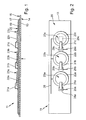
- FIG. 1 an operating device 11 according to the invention is shown, as it can be used for example for an aforementioned electrical appliance or may be part of it.
- the operating device 11 has a diaphragm 13, for example as a large-area diaphragm of the electrical appliance.
- the panel can be made of plastic or sheet metal, for example stainless steel. It has a front side 14, at the center of which a force represented by an arrow is applied. This force can be generated by an operator by placing or pressing with a finger on the front side 14.
- a circuit board 19 as a support for piezo sensor elements 22 attached.
- the piezo sensor elements 22a to c are applied to the rear side 20 of the printed circuit board 19.
- you could basically with a coating process such as screen printing or the like. be applied as thick-film components directly on the circuit board 19.
- they are produced as separate components, for example, as described above from a piezo ceramic disk and a metal diaphragm, and then attached to the circuit board 19.
- As attachment offers an adhesive, in particular with an electrically conductive adhesive.
- An electrical contact to a piezo-sensor element 22 takes place on the one hand on its upper side 23, which will be explained in more detail below.
- the contact pads 25 and ground contact track 26 are applied as conventional copper tracks on the circuit board 19 and connect the ground terminal of all piezo sensor elements 22 together. Then, the piezo sensor element 22 is applied to this contact pad 25, which may also be designed differently in size, preferably glued.
- contact fields 28a to c which each have connection printed conductors 29a to c.
- These contact fields 28 together with connecting conductor tracks 29 are applied to the printed circuit board 19 like the above-described contact pads 25 together with the conductor track 26, advantageously as copper tracks.
- These are U-shaped bent, like out Fig. 1 can be seen, and consist of thin elastic copper sheet. One end is attached to a contact pad 28, for example, soldered firmly. The other end is biased to the top 23. Again, a firm connection is possible, for example by soldering or gluing.
- Each individual piezoelectric sensor element 22 a to c can be individually controlled or evaluated via the connecting strip conductors 29 a to c.
- the assembly of both the piezo sensor elements 22 and the contact clip 31 can be automated with the possibility of rapid and precise production in large quantities.
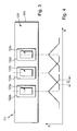
- Fig. 3 is a plan view of a further operating device 111 is shown, which also has three piezo-sensor elements 122a-c. Their electrical connections are not shown for the sake of clarity, but they can according to those of the operating device 11 according to the Fig. 1 and 2 be educated. Furthermore, in a modification to the other operating device, a rectangular shape is provided for the piezo sensor elements 122 here.
- the control device 111 is not only the respective, so to speak punctiform triggering an operating function by applying a force due to placing a finger on the front of the aperture relatively centrally above a piezo-sensor element recognize. It should also be possible to pull an applied and pressed finger over the area of the piezo sensor elements 122.
- Such a control device is just called slider and is, for example, from the principle of the DE 102004024835 B3 , of the DE 102004044355 or the DE 102005018298 basically known. This linear or pulling movement can then be linked to various operating functions, but this does not matter for the present patent application. In the present patent application, it is more about the structural design of such an operating device and, especially in connection with a plurality of juxtaposed sensor elements to the realization or, above all, evaluation of such a slider function.
- Fig. 1 also causes a deflection of the diaphragm, although this can be very low, for example in the micron range.
- This deflection of the diaphragm also causes a deflection of the circuit board and thus also the piezo sensor elements, which can be well evaluated.
- it is not completely avoidable, especially with relatively stiff materials for the diaphragm that not only via a single piezo sensor element, which is to be actuated so to speak, but also over adjacent sensor elements results in a deflection and thus also here a signal swing is generated, although this is much lower.
- a slider function as in Fig.
- Fig. 5 is a modification of Fig. 3 shown with an operating device 211 including the printed circuit board 213.
- piezo-sensor elements 222 with upper sides 223 are compared to the longitudinal axis along which both in Fig. 3 as well as in Fig. 5 the sensor elements are tilted by about 30o. Since the deflection of the diaphragm when exercising the finger pressure is not only purely punctiform, but extends over a certain range, and this area when moving along the longitudinal direction of the arrangement of the piezo sensor element 222, so to speak, also a certain extent perpendicular has to this direction of movement, overlap the sensor elements or tapped at them signal strokes S stronger. This is from the diagram Fig.
- Fig. 7 is shown in the circuit diagram, as an impedance conversion in a method for signal evaluation of a piezo-sensor element 22 may be formed. It can be seen how the ground contact strip 26 is guided via a resistor R3 to ground, while a DC voltage source V1 is connected thereto via the resistor R1. Via the resistor R5 ground contacts 26 and terminals 29 are connected. Furthermore, this connection goes to the base of a transistor T1 and is also grounded via the capacitor C1. The supply voltage V1 is applied to the transistor T1 via the resistor R2, and at the same time it is connected to ground via a resistor R4. A signal output T Out1 goes from the circuit to an input In 1 of a controller 33, which is formed in a microcontroller. Furthermore, signal outputs of the other piezo sensor elements 22 go to the controller 33 as well, as shown by the signal output T Out2 . The function of this impedance conversion is easy to understand.
- Fig. 8 is shown how detached from a signal processing on a single piezo-sensor element 22 with a differential measuring method according to the invention signals can be evaluated.
- the evaluation can thus be improved both in the case of a punctiform actuation and in the case of an aforementioned slider actuation.
- a first piezo sensor element 22a is connected via a connection 29a to the negative input of an OP amplifier 35a.
- the terminal 29b of a second piezo sensor element 22b is connected both to the plus input of the same OP amplifier 35a and to the minus input of a second OP amplifier 35b.
- the terminal 29c of a third piezo sensor element 22c is connected to the plus input of the OP amplifier 35b. This can be continued as desired for further piezo sensor elements.
- the output signal with the difference of the signals of the second piezo sensor element 22b and the first piezo sensor element 22a forms the output of the OP amplifier 35a.
- the OP amplifier 35b it is the difference between the signals of the third piezo sensor element 22c and of the second piezo sensor element 22b.
- An essential feature for trouble-free and interference-free operation of the operating device is intelligent signal conditioning. Disturbances can be EMC influences such as burst exposure be. Since the operating device described here is based on piezo technology, it is, so to speak, an acoustic unit which is also exposed to acoustic interference. These are diverse and can be structure-borne noise by engine hum, knock on the control panel, airborne noise, etc.
- a method for eliminating the interference can be applied by forming the signal difference described between adjacent sensor elements. With the same signal change due to interference, the signal sum then becomes zero. However, if a sensor element is actuated properly, it experiences a different signal swing than the adjacent sensor elements and the signal difference is clearly positive or negative, depending on the pressures or letting go of the sensor element.
- the disturbance compensation can be carried out by subtracting usefully in the microcontroller cost.
- an electronic circuit is then only for each sensor element according to a Impendanzwandlung Fig. 7 required, which already includes a signal amplification.
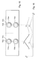
- an operating device 311 is shown, which is basically similar to that of Fig. 3 , However, here the piezo sensor elements 322a, 322b and 322c are aligned with their longitudinal direction not transverse to the extension direction corresponding to the Berlickweg B, but in the longitudinal direction thereof. So you are in proportion to Fig. 3 rotated by 90 ° and have a smaller distance from each other.
- Fig. 3 rotated by 90 ° and have a smaller distance from each other.
- the corresponding diagram of the signal stroke S over the Bermm B according to Fig. 10 is shown in each case for the Y direction and for the X direction of the signal swing S.
- each of these rows of the array Fig. 9 corresponds and is only slightly narrower.
- the piezo sensor elements 422a, 422b and 422c extend.
- the further enhanced directional sensitivity causes a keystroke in the center of the key can be very well located and detected when the signal swing S of the upper piezo-sensor element and the lower is equal or nearly equal. However, as soon as the signal strokes differ more clearly, the signal or the keystroke is discarded. Then, a location of the contact path B tends to deviate too far in the Y direction from the line of the contact path B and then no longer corresponds to a proper contact or operation.
- each stacked two separate piezo sensor elements it is also possible to use a single piezo-part and to attach two separate tops or these generally forming electrodes as a signal tap. This then corresponds purely functional two piezo sensor elements, only the mechanical or design effort is slightly reduced.
- a bipartite element is made from a piezo-sensor element, as it were, with the expenditure and the possibilities of a double signal evaluation, but only the design complexity of a single sensor element or piezoceramic substrate.
- a dividing line 524 between the tops 523a and 523b, or between the electrodes covering them generally, would then be similar in arrangement Fig. 11 in the direction of Bermmweges B, ie in the X direction aligned.
- the advantage of this design is that a very precise differential measurement is possible because the sensors are, so to speak, paired on the same piezoceramic substrate. Voltage tolerances that differ from disc thickness, polarization, bonding, ambient temperature or the like. can occur while doing so. For the same deflection when actuated along the dividing line 524, the same voltage U Hx and U Hx ' is produced on the two upper sides 523a and 523b.
- a division of the upper side of the piezo sensor element instead of a division of the upper side of the piezo sensor element also an even finer division can be made.
- This can be, for example, a tetrants or quadrants division, that is, in three or four equally sized circle segments.
- FIG. 14 A so-called optimized variant of such a three-part piezo sensor element is in Fig. 14 shown.
- a disk-shaped piezo sensor element 622 arranged on a metallic contact pad 625. It has three top portions 623a, 623b and 623c, each identically formed and separated by dividing lines 624a to 624c.
- the course of the tops 623 is difficult to describe. In essence, however, their design is such that they first run counterclockwise about a third of the circumference of the outer edge of the piezo sensor element 622 along and then in the same direction of rotation inwardly into a kind of inner tetrants surface in the manner of a circle segment.
- the tops 623 are thus very short screw-line pieces that are drawn inwardly with an enlarged inner end.
- the effective diameter and thus the piezoelectric voltage U H can be increased, in each case in the in Fig. 14 indicated directions. Since the electrode voltage, which can be picked up at the sensor element or prevails between contact field 625 and upper side 623, is proportional to the diameter of the piezo sensor element 622, it is advantageous if the segments of the upper sides 622 have the largest possible effective diameter perpendicular to the bending line , With the same deflection along such a bending line, the same voltage U H arises on two opposite upper sides 623, that is to say, for example, 623 a and 623 c.
- the deflection is the same when the key press takes place exactly in the middle between the two electrodes. Since this can be evaluated for each two opposite top pairs, can be done with the effort of revaluation of three voltages positionally accurate centric position location of the keystroke or the place of operation and the laying on of a finger. Such training is also possible either with less or even higher distribution.
- FIG. 15 a further modification of an operating device 711 is shown. This corresponds again approximately to those from Fig. 11 , wherein by the four sensor elements 722a, 722a 'one above the other and 722b, 722b' one above the other, a kind of planar control panel is created.
- Fig. 16 It is according to Fig. 16 to recognize how at a marked pressure point near the piezo sensor element 722a whose signal swing S is greater than the other.
- a two-dimensional localization can take place via the ratio of the four individual signal levels or signal strokes S of the individual piezo sensor elements. This can be done not only in addition to an operation or actuation in one direction or along a line an evaluation, but also over an area away.
- Effort can be saved by omitting piezo sensor elements.
- a further direction for an operation can be added for extended operating possibilities.
- FIG. 17 is another operating device 811 not belonging to the claimed invention, shown with a bezel 813 and a front side 814, as substantially similar Fig. 1 is constructed.
- a printed circuit board 819 which is designed as a support for piezo sensor elements 822a, 822b and 822c on its rear side 820, is fastened to a rear side 815 of the cover 813 by means of an adhesive layer 817.
- interconnects 826 or corresponding copper fields or contact fields on the one hand and 826a 'and 826b' on the other hand are provided for the individual piezo sensor elements 822.
- FIG. 18 In the greatly enlarged sectional view according to FIG Fig.
- solder 827 On the back 820 of the circuit board 819 are on the tracks 826 and 826 'by means of solder 827, which may alternatively be a conductive adhesive, so an electrically conductive adhesive, the piezo-sensor elements 822 attached. This is done in such a way that a piezo ceramic disk 837 is mechanically fastened to the conductor tracks 826 'by means of solder 827 and is electrically connected thereto.
- the piezo ceramic disks 837 are advantageously provided with a thin metallization, for example a silver layer.
- the metal diaphragm 838 of the piezoelectric sensor element 822 which is permanently connected to the piezoceramic disk 837 by gluing or the like, is electrically connected in its outer region to a lower side by means of solder 827 with the conductor tracks 826 and mechanically fastened.
- solder 827 with the conductor tracks 826 and mechanically fastened.
- a conductive adhesive can be used.
- the conductor track 826 may be formed, for example, in the manner of a partial circle and the printed conductors 826 'or contact fields are substantially surrounded by an interruption, so that these according to FIG Fig. 18 can be led out.
Landscapes
- Electronic Switches (AREA)
- Force Measurement Appropriate To Specific Purposes (AREA)
- Push-Button Switches (AREA)
- Switches That Are Operated By Magnetic Or Electric Fields (AREA)
- Apparatus For Radiation Diagnosis (AREA)
Description
Die Erfindung betrifft eine Bedieneinrichtung für ein Elektrogerät, wobei die Bedieneinrichtung ein formveränderliches bzw. elastisches BedienFeld aufweist, unter dem mindestens ein Piezo-Sensorelement angeordnet ist.The invention relates to an operating device for an electrical appliance, wherein the operating device has a dimensionally variable or elastic control panel, under which at least one piezo sensor element is arranged.
Aus der
Aus der
In der
Aus der
Aus der
Die
Der Erfindung liegt die Aufgabe zugrunde, eine eingangs genannte Bedieneinrichtung zu schaffen, mit der Nachteile des Standes der Technik vermieden werden können und insbesondere sowohl Anordnung als auch Anschluss leicht und sicher möglich sind, auch bei einer größeren Anzahl von Piezo-Sensorelementen.The invention has for its object to provide a control device mentioned above, with the disadvantages of the prior art can be avoided and in particular both arrangement and connection are easily and safely possible, even with a larger number of piezo sensor elements.
Gelöst wird diese Aufgabe durch eine Bedieneinrichtung mit den Merkmalen des Anspruchs 1. Vorteilhafte sowie bevorzugte Ausgestaltungen der Erfindung sind Gegenstand der weiteren Ansprüche und werden im Folgenden näher erläutert.This object is achieved by an operating device with the features of
Gemäß der Erfindung ist vorgesehen, dass das wenigstens eine Piezo-Sensorelement auf der Rückseite einer Leiterplatte angeordnet ist, insbesondere daran befestigt ist. Die Leiterplatte wird mit der gegenüberliegenden Vorderseite flächig an der Unterseite des Bedien-Feldes angebracht bzw. daran angeordnet und befestigt. Somit wird also das Piezo-Sensorelement nicht direkt an der Unterseite des Bedien-Feldes befestigt, was insbesondere bei einer größeren Anzahl von Piezo-Sensorelementen aufwändig ist, sondern indirekt. Dabei kann vorteilhaft vorgesehen sein, dass das Bedien-Feld Teil eines Rahmens oder einer Frontblende des Elektrogerätes ist bzw. einen Teil davon bildet. Die Befestigung des mindestens einen Piezo-Sensorelementes an der Leiterplatte kann durch herkömmliche, großserientechnisch erprobte Verfahren erfolgen, wie sie gerade bei Bestückung von Leiterplatten bekannt sind. Des weiteren kann dann die Leiterplatte mit dem mindestens einen Piezo-Sensorelement als Baueinheit soweit vorgefertigt werden, dass diese Baueinheit beim Zusammenbau des Elektrogerätes nur noch mit dem Bedien-Feld bzw. Rahmen oder Frontblende eines Elektrogerätes verbunden werden muss bzw. daran befestigt wird. So ist ein präziser Aufbau der Bedieneinrichtung gut möglich mit präziser Funktion, für die hier der mechanische Aufbau wichtig ist.According to the invention it is provided that the at least one piezo-sensor element is arranged on the back of a printed circuit board, in particular attached thereto. The circuit board is opposite Front surface mounted on the underside of the control panel or arranged and attached thereto. Thus, therefore, the piezoelectric sensor element is not attached directly to the underside of the control panel, which is complex especially in a larger number of piezo sensor elements, but indirectly. It can be advantageously provided that the control panel is part of a frame or a front panel of the electrical appliance or forms part of it. The attachment of the at least one piezo-sensor element to the circuit board can be done by conventional, mass-production technology proven method, as they are currently known in the assembly of printed circuit boards. Furthermore, the printed circuit board with the at least one piezoelectric sensor element can then be prefabricated as a unit so far that this assembly only has to be connected to the control panel or frame or front panel of an electrical appliance during assembly of the electrical appliance or attached thereto. Thus, a precise structure of the operating device is well possible with precise function, for which the mechanical structure is important here.
Vorteilhaft können auf der Leiterplatte mehrere Piezo-Sensorelemente für mehrere Bedienelemente vorgesehen sein. Besonders vorteilhaft sind, möglicherweise bis auf die Ausnahme eines mechanischen Ein-/Ausschalters, alle Bedienelemente der Bedieneinrichtung durch derartige, insbesondere gleichartige, Piezo-Sensorelemente realisiert. Dies vereinfacht den Herstellungsaufwand. Dabei können mehrere Piezo-Sensorelemente bei ausreichend genauer Bedienbarkeit relativ nahe beieinander angeordnet werden. Es ist sogar möglich, ihren Abstand zueinander geringer zu halten als Länge oder Breite eines solchen Piezo-Sensorelementes. So lassen sich auch linienartige Bedien-Elemente bilden, die auch als "Slider" bekannt sind und deren Realisierung mit kapazitiven Sensorelementen beispielsweise aus der
Ein Piezo-Sensorelement für die Bedieneinrichtung ist erfindungsgemäß scheibenartig bzw. als dünne oder flache Scheibe ausgebildet. Mit einer seiner flachen Seiten ist das Sensorelement dann auf der Leiterplatte befestigt, beispielsweise festgeklebt oder verlötet. Bei der Erfindung weist ein Piezo-Sensorelement eine Piezo-Keramikscheibe auf. Diese Piezo-Keramikscheibe ist mit einer Metallmembran verbunden, insbesondere sind sie miteinander verklebt. Das Piezo-Sensorelement weist sowohl auf seiner Oberseite als auch auf seiner Unterseite einen elektrischen Anschluss auf. Vorteilhaft ist dies ein flächiger Anschluss, was auf beiden Seiten den Anschluss bzw. die elektrische Kontaktierung erleichtert. Grundsätzlich ist ein derartiger Aufbau eines Piezo-Sensorelements bekannt.A piezo-sensor element for the operating device according to the invention is disc-like or formed as a thin or flat disc. With one of its flat sides, the sensor element is then mounted on the circuit board, for example glued or soldered. In the invention, a piezo sensor element has a piezo ceramic disk. This piezo ceramic disk is connected to a metal diaphragm, in particular, they are glued together. The piezo sensor element has an electrical connection both on its upper side and on its lower side. This is advantageous a flat connection, which facilitates the connection or the electrical contact on both sides. Basically, such a construction of a piezo sensor element is known.
Auf der Leiterplatte sind an einer Stelle, an der ein Piezo-Sensorelement sein soll, Kontaktfelder vorgesehen. Diese sind insbesondere als Leiterbahnen auf der Leiterplatte ausgebildet bzw. damit verbunden, wobei davon wegführende Kontaktleitungen ebenfalls als Leiterbahnen vorgesehen sein können. Zur elektrischen Kontaktierung wird also ein Piezo-Sensorelement auf dem Kontaktfeld befestigt, wozu vorteilhaft ein elektrisch leitfähiger Kleber als sogenannter Leitkleber verwendet werden kann, alternativ kann gelötet werden. Ein solches Aufkleben ermöglicht eine sowohl zuverlässige Befestigung als auch eine leichte Herstellung der elektrischen Verbindung.On the circuit board, contact fields are provided at a location where a piezo sensor element is to be. These are in particular formed as conductor tracks on the printed circuit board or connected thereto, wherein it can also be provided as conductor tracks away leading contact lines. For electrical contacting, therefore, a piezoelectric sensor element is mounted on the contact pad, for which purpose an electrically conductive adhesive can be used as so-called conductive adhesive, alternatively it can be soldered. Such sticking enables both reliable attachment and easy production of the electrical connection.
Eine weitere bzw. die zweite elektrische Kontaktierung hat das Piezo-Sensorelement erfindungsgemäß an der von der Leiterplatte weg weisenden Seite, und diese erfolgt durch einen Kontaktbügel. Ein solcher Kontaktbügel reicht von einem weiteren elektrischen Anschlussfeld samt Anschlussleitung, insbesondere wiederum als Leiterbahn auf der Leiterplatte, auf die freiliegende Seite bzw. Oberseite des Piezo-Sensorelementes. Auch ein Bonding-Verfahren ist eine Möglichkeit, also mit einem Bonding-Draht als Kontaktbügel. Der Kontaktbügel kann auch ein Standard-SMD-Bauelement sein, beispielsweise ein 0-Ohm SMD-Widerstand.Another or the second electrical contact has the piezoelectric sensor element according to the invention on the facing away from the circuit board side, and this is done by a contact clip. Such a contact clip extends from a further electrical connection field together with the connecting line, in particular again as a conductor track on the printed circuit board, to the exposed side or upper side of the piezoelectric sensor element. Also, a bonding process is a possibility, so with a Bonding wire as a contact clip. The contact clip may also be a standard SMD component, for example a 0-ohm SMD resistor.
Hier kann vorgesehen sein, dass dieser weitere elektrische Anschluss an der frei liegenden Seite des Piezo-Sensorelementes jeweils ein Anschluss an eine Auswerteeinrichtung ist, der für jedes Piezo-Sensorelement einzeln vorhanden ist. Der andere Anschluss, der direkt über ein Kontaktfeld auf der Leiterplatte an das Sensorelement erfolgt, kann dann ein gemeinsamer Masseanschluss sein. Dies kann selbstverständlich auch andersherum gemacht werden. Der Vorteil eines gemeinsamen Masseanschlusses an die frei liegende Seite der Piezo-Sensorelemente liegt darin, dass hier ein Mehrfach-Kontaktbügel verwendet werden kann. Dieser kann so ausgebildet sein, dass er bei einem oder zwei Befestigungspunkten an der Leiterplatte mehrere Sensorelemente kontaktiert, insbesondere alle. Ein elektrischer Kontakt eines solchen Kontaktbügels an die frei liegende Seite des Piezo-Sensorelementes kann entweder einfach durch Aufdrücken mit Anliegen erfolgen oder durch eine Verklebung mit elektrisch leitfähigem Kleber.Here it can be provided that this further electrical connection on the exposed side of the piezo sensor element is in each case a connection to an evaluation device which is provided individually for each piezo sensor element. The other connection, which takes place directly via a contact pad on the circuit board to the sensor element, can then be a common ground connection. Of course, this can also be done the other way round. The advantage of a common ground connection to the exposed side of the piezo sensor elements is that a multiple contact clip can be used here. This can be designed so that it contacts a plurality of sensor elements at one or two attachment points on the circuit board, in particular all. An electrical contact of such a contact clip to the exposed side of the piezoelectric sensor element can either be done simply by pressing with concern or by a bond with electrically conductive adhesive.
Ein Kontaktbügel oder Mehrfach-Kontaktbügel kann beispielsweise als einfache Metallklammer aus Draht oder einem flachen Blechstreifen ausgebildet sein.A contact clip or multiple contact clip may be formed, for example, as a simple metal clip made of wire or a flat sheet metal strip.
Alternativ zu einer ober- und unterseitigen Kontaktierung des Sensorelements können beide Kontaktierungen auch von einer Seite erfolgen, indem das Piezo-Sensorelement auf der Leiterplatte derart angeordnet ist, daß einerseits eine Anschlußfläche der Piezo-Keramikteils des Piezo-Sensorelements zur Leiterplatte zeigt und direkt mit der Leiterplatte verlötet und/oder verklebt wird. Andererseits wird die ebenfalls zur Leiterplatte hin zeigende überstehende Restringfläche einer Metallmembran, auf die das Piezo-Keramikelement geklebt ist, ebenfalls direkt mit der Leiterplatte verlötet bzw. verklebt und somit elektrisch kontaktiert. Dadurch kann eine oberseitige Kontaktierung entfallen. Als besonderer Vorteil kann dadurch die gesamte Montage und Kontaktierung des Piezo-Sensorelementes in einem Löt- bzw. Klebearbeitsvorgang durchgeführt werden.As an alternative to a top and bottom contact of the sensor element both contacts can also be made from one side by the piezoelectric sensor element is arranged on the circuit board such that on the one hand shows a pad of the piezo ceramic part of the piezoelectric sensor element to the circuit board and directly with the Printed circuit board soldered and / or glued. On the other hand, the projecting towards the circuit board protruding residual annular surface of a metal membrane, on which the piezo-ceramic element is glued, also directly with the Printed circuit board soldered or glued and thus contacted electrically. As a result, a top-side contact can be omitted. As a particular advantage, the entire assembly and contacting of the piezo sensor element can be carried out in a soldering or gluing process.
Auf der von der Leiterplatte weg weisenden Seite des Piezo-Sensorelements kann zur elektrischen Kontaktierung eine Aufteilung in mehrere elektrisch leitfähige Flächen vorgesehen sein, die jeweils getrennt voneinander angeschlossen sind. So kann ein einzelnes Piezo-Keramikteil funktional in mehrere Sensoren aufgeteilt werden, beispielsweise zwei, drei oder vier Sensoren. Die mehreren elektrisch leitfähigen Flächen können vorteilhaft eine Form aufweisen, die von einer geradlinig geteilten Kreis- oder Rechteckform abweicht. Dabei können solchermaßen gebildete Teil-Flächen ineinander verschlungen sein. So ist eine besonders gute verstärkte Empfindlichkeit in abweichende Richtungen erreichbar.On the side facing away from the circuit board side of the piezoelectric sensor element can be provided for electrical contacting a division into a plurality of electrically conductive surfaces, which are each connected separately. Thus, a single piezo ceramic part can be divided functionally into several sensors, for example two, three or four sensors. The plurality of electrically conductive surfaces may advantageously have a shape which deviates from a rectilinearly divided circular or rectangular shape. In this case, part-surfaces formed in this way can be intertwined. Thus, a particularly good increased sensitivity in different directions can be achieved.
Grundsätzlich können Piezo-Sensorelemente als Bedien-Elemente an der Bedieneinrichtung frei platziert werden. Vorteilhaft wird mindestens eine Linie von Piezo-Sensorelementen gebildet, insbesondere um ein insgesamt längliches linienartiges Bedienelement nach Art des genannten Sliders zu bilden. Die Reihe von Piezo-Sensorelementen kann in einfacher Ausbildung gerade verlaufen, alternativ auch gekrümmt bzw. bogenartig sein.In principle, piezo sensor elements can be freely placed as operating elements on the operating device. Advantageously, at least one line of piezo sensor elements is formed, in particular in order to form an overall elongated linear control element in the manner of the named slider. The series of piezo sensor elements can be straight in a simple design, alternatively also be curved or bow-shaped.
In vorteilhafter Weiterbildung der Erfindung können mehrere Piezo-Sensorelemente, insbesondere alle, in mehreren fortlaufenden und parallelen Reihen angeordnet sein. Besonders vorteilhaft sind dies zwei Reihen, wobei insbesondere jeweils Piezo-Sensorelemente sich gegenüberliegend angeordnet sind in den Reihen.In an advantageous embodiment of the invention, a plurality of piezo sensor elements, in particular all, can be arranged in a plurality of continuous and parallel rows. These are particularly advantageous two rows, in particular each piezo-sensor elements are arranged opposite one another in the rows.
Wie bereits erläutert worden ist, sind vorteilhaft mehrere Piezo-Sensorelemente an der Bedieneinrichtung vorgesehen. In vorteilhafter Ausgestaltung der Erfindung sind sie sämtlich identisch ausgebildet. Sie können eine länglich-rechteckige Form aufweisen mit einer langen Seite und einer kurzen Seite, wobei bei einer vorteilhaften Ausgestaltung der Erfindung ihre langen Seiten nebeneinander liegen. Dies ist in Verbindung mit einem vorbeschriebenen sehr geringen Abstand zwischen den Piezo-Sensorelementen vor allem dazu geeignet, einen vorgenannten Slider zu bilden. Hierfür kann in nochmals weiterer Ausgestaltung der Erfindung vorteilhaft vorgesehen sein, dass die Piezo-Sensorelemente zwar mit ihren langen Seiten benachbart und im Wesentlichen parallel zueinander angeordnet sind. Allerdings sind diese langen Seiten in einem Winkel zwischen 15° und 90° zu einer Linie verdreht, vorzugsweise zwischen 45° bis 60° und 80°, entlang derer die Piezo-Sensorelemente ungefähr angeordnet sind. Wenn zur Bedienung ein Finger mit einer gewissen Fläche über diese Linie durch Auflegen bewegt wird, kann dadurch erreicht werden, dass dieser Finger bzw. seine Position von mindestens einem Piezo-Sensorelement erfasst werden kann, weil er sich darüber befindet. Er kann also sozusagen nicht in der Abstandslücke zwischen zwei Sensorelementen untergehen oder nicht gefunden bzw. festgestellt werden. Die Piezo-Sensorelemente können aber auch wahlweise beliebig und ungeordnet auf der Leiterplatte angeordnet sein.As has already been explained, several piezo sensor elements are advantageously provided on the operating device. In an advantageous embodiment of the invention, they are all identical. They may have an oblong-rectangular shape with a long side and a short side, wherein in an advantageous embodiment of the invention, their long sides are adjacent. This is particularly suitable in conjunction with a prescribed very small distance between the piezo sensor elements to form an aforementioned slider. For this purpose, it can be advantageously provided in a further embodiment of the invention that the piezo sensor elements are indeed adjacent with their long sides and arranged substantially parallel to each other. However, these long sides are twisted at an angle between 15 ° and 90 ° to a line, preferably between 45 ° to 60 ° and 80 °, along which the piezo sensor elements are approximately arranged. If, for operation, a finger with a certain surface is moved over this line by being placed on it, it can be achieved that this finger or its position can be detected by at least one piezo sensor element because it is above it. So it can not go down in the distance gap between two sensor elements so to speak or not found or found. However, the piezo sensor elements can also be arranged arbitrarily and randomly on the printed circuit board.
Bei der Anordnung der Bedieneinrichtung an dem Bedien-Feld kann vorgesehen sein, die Baueinheit aus Leiterplatte und Piezo-Sensorelementen mittels eines doppelseitig klebenden Klebebandes mit ihrer Vorderseite an der Rückseite des Bedien-Feldes festzukleben und zu befestigen. Ein solches doppelseitiges klebendes Klebeband kann nach Art einer Folie ausgebildet sein und sollte eine geringe Dicke aufweisen, vorteilhaft etwa 0,2 mm oder 0,1 mm oder sogar noch weniger. Durch die Dicke des Klebebandes kann ein Ausgleich von Toleranzen erfolgen. Ein solches doppelseitiges Klebeband ermöglicht bei werkseitiger Anbringung an der Bedieneinrichtung eine Vormontage der Befestigung bzw. Verklebung. Die Verklebung kann hier alternativ durch Kleberauftrag mit einem flächig aufgetragenen Klebefilm erfolgen. Eine Verklebung allgemein weist den Vorteil auf, dass eine Tastendruck-sensitive, starre Ankopplung der Leiterplatte an die Bedienblende gewährleistet wird.In the arrangement of the operating device on the control panel can be provided to stick the assembly of printed circuit board and piezo sensor elements by means of a double-sided adhesive tape with its front on the back of the control panel and secure. Such a double-sided adhesive tape may be formed in the manner of a film and should have a small thickness, advantageously about 0.2 mm or 0.1 mm or even less. Due to the thickness of the adhesive tape, a compensation of tolerances can take place. Such a double-sided adhesive allows for factory attachment at the operating device, a pre-assembly of the attachment or bonding. The bonding can be done here alternatively by adhesive application with a surface applied adhesive film. An adhesive bond in general has the advantage that a keystroke-sensitive, rigid coupling of the printed circuit board to the control panel is ensured.
Durch die Anordnung der Piezo-Sensorelemente an der Leiterplatte und durch deren Anordnung an der Rückseite des Bedien-Feldes wiederum kann durch Ausnutzung einer wenn auch geringen Durchbiegung des Bedien-Feldes durch Auflegen eines Fingers odgl. darauf und Übertragung dieser Biegung auf das Piezo-Sensorelement auf ein Gegenlager für die Sensorelemente verzichtet werden, wie dies ansonsten für eine solche Bedieneinrichtung notwendig ist. Der Stand der Technik in Form der
In weiterer Ausgestaltung der Erfindung kann vorgesehen sein, dass das Bedien-Feld Durchbrüche aufweist, hinter denen Leuchtanzeigen angeordnet sind. Derartige Leuchtanzeigen können mittels LED realisiert sein und vor allem dann die Durchbrüche benötigen, wenn das Bedien-Feld aus Metall oder einem anderen lichtundurchlässigen Material besteht. Derartige Leuchtanzeigen in Form beispielsweise von LED oder Sieben-Segment-Anzeigen können ebenfalls auf der Leiterplatte angeordnet sein, die auch die Piezo-Sensorelemente trägt. Die Erfindung eignet sich besonders gut für Bedien-Felder aus Metall, insbesondere Edelstahl oder Aluminium. Deren Dicke kann etwa einen Millimeter betragen oder weniger, unter Umständen auch etwas mehr. Vorteilhaft ist im Bereich der Piezo-Sensorelemente die Materialdicke gleichbleibend ohne eine Reduzierung, so dass die Herstellung eines solchen Bedien-Feldes aus einem einzigen Metallteil vereinfacht ist. Durch den erfindungsgemäßen Aufbau der Bedieneinrichtung kann auch bei relativ dicken und somit relativ steifen Bedien-Feldern das Auflegen eines Fingers mit nicht allzu großer Kraft, beispielsweise 1 N oder sogar noch deutlich darunter mittels eines Piezo-Sensorelements sowohl allgemein erkannt werden als auch konkret bezüglich des Ort des Auflegens bei mehreren, eng benachbarten Piezo-Sensorelementen unterschieden werden. Es können aber auch große Tastendrücke, beispielsweise deutlich größer als 10 N aufgenommen, beispielsweise werden für vandalensichere Tastaturen.In a further embodiment of the invention can be provided that the control panel has openings behind which light indicators are arranged. Such lights can be realized by means of LED and especially then require the breakthroughs when the control panel is made of metal or other opaque material. Such lights in the form of, for example, LED or seven-segment displays can also be arranged on the circuit board, which also carries the piezo sensor elements. The invention is particularly well suited for control panels made of metal, in particular stainless steel or aluminum. Their thickness can be about one millimeter or less, possibly a little more. It is advantageous in the area the piezo sensor elements, the material thickness consistent without reduction, so that the production of such a control panel is simplified from a single metal part. Due to the inventive design of the operating device, the laying on of a finger with not too great force, for example 1 N or even significantly lower by means of a piezoelectric sensor element can be recognized both generally and concretely with respect to the relatively large and thus relatively stiff control panels Place of laying on several, closely adjacent piezo sensor elements are distinguished. But it can also large keystrokes, for example, recorded much larger than 10 N, for example, are for vandal-proof keyboards.
In weiterer Ausgestaltung der Erfindung weist die Bedieneinrichtung vorteilhaft eine Signalauswertung auf, die auch gleichzeitig eine Ansteuerung für die Sensorelemente sein kann. In Weiterbildung der Erfindung können in der Signalauswertung Differenziermittel vorgesehen sein, die eine Signaldifferenz zwischen zwei benachbarten Piezo-Sensorelementen bilden. Dazu sind die Differenziermittel jeweils mit den Sensorelementen verbunden, wobei ein Ausgang eines solchen Differenziermittels einer weiteren Bearbeitung bzw. Auswertung zugeführt wird. Vorteilhaft kann vorgesehen sein, dass die Bedieneinrichtung mindestens drei Piezo-Sensorelemente aufweist und jeweils zwei direkt benachbarte Piezo-Sensorelenente mit jeweils einem Differenziermittel verbunden sind. So können also das erste und das zweite Sensorelement mit einem ersten Differenziermittel verbunden sein, das zweite und das dritte Sensorelement mit einem zweiten Differenziermittel, usw. Der Ausgang benachbarter Differenziermittel wird dann an eine Signalauswertung gegeben um festzustellen, an welchem Sensorelement bzw. an welcher Stelle die größte Signaländerung stattgefunden hat. Als Differenziermittel können hier vorteilhaft Operationsverstärker vorgesehen sein, die eine nachgeschaltete Signalverstärkung zur sicheren Erkennung aufweisen können. In alternativer Ausgestaltung der Erfindung können die Differenziermittel nicht mit diskreten Bauteilen wie OP-Verstärkern aufgebaut sein, sondern in einem Mikrokontroller, der auch für die Signalauswertung verwendet werden kann. Das Ergebnis einer Impedanzwandlung kann eben dann, wenn keine separaten OP-Verstärker vorgesehen sind, direkt an einen A/D-Wandlereingang eines Mikrokontroller gegeben werden.In a further embodiment of the invention, the operating device advantageously has a signal evaluation, which can also be a control for the sensor elements at the same time. In a development of the invention, differentiating means can be provided in the signal evaluation, which form a signal difference between two adjacent piezo sensor elements. For this purpose, the differentiating means are each connected to the sensor elements, wherein an output of such differentiating means is supplied to a further processing or evaluation. Advantageously, it can be provided that the operating device has at least three piezo sensor elements and in each case two directly adjacent piezo sensor elements are each connected to a differentiating means. Thus, therefore, the first and the second sensor element may be connected to a first differentiating means, the second and the third sensor element with a second differentiating means, etc. The output of adjacent differentiating means is then connected to a Signal evaluation given to determine at which sensor element or at which point the largest signal change has taken place. Advantageously, operational amplifiers may be provided as differentiating means, which may have a downstream signal amplification for reliable detection. In an alternative embodiment of the invention, the differentiating means can not be constructed with discrete components such as OP amplifiers, but in a microcontroller, which can also be used for signal evaluation. The result of an impedance conversion can be given directly to an A / D converter input of a microcontroller, even if no separate OP amplifiers are provided.
Diese und weitere Merkmale gehen außer aus den Ansprüchen auch aus der Beschreibung und den Zeichnungen hervor, wobei die einzelnen Merkmale jeweils für sich allein oder zu mehreren in Form von Unterkombination bei einer Ausführungsform der Erfindung und auf anderen Gebieten verwirklicht sein und vorteilhafte sowie für sich schutzfähige Ausführungen darstellen können, für die hier Schutz beansprucht wird. Die Unterteilung der Anmeldung in einzelne Abschnitte sowie Zwischen-Überschriften beschränken die unter diesen gemachten Aussagen nicht in ihrer Allgemeingültigkeit.These and other features will become apparent from the claims but also from the description and drawings, wherein the individual features each alone or more in the form of sub-combination in one embodiment of the invention and in other areas be realized and advantageous and protectable Represent embodiments for which protection is claimed here. The subdivision of the application into individual sections as well as intermediate headings does not restrict the general validity of the statements made thereunder.
Ausführungsbeispiele der Erfindung sind in den Zeichnungen schematisch dargestellt und werden im Folgenden näher erläutert. In den Zeichnungen zeigen:
- Fig. 1
- eine seitliche Schnittdarstellung durch eine erste Ausbildung einer erfindungsgemäßen Bedieneinrichtung mit Piezo-Sensorelementen auf einer Leiterplatte an der Rückseite einer Blende,
- Fig. 2.
- eine Rückansicht der Bedieneinrichtung aus
Fig. 1 mit Darstellung des elektrischen Anschlusses der Piezo-Sensorelemente, - Fig. 3
- eine alternative Bedieneinrichtung in vereinfachter Darstellung entsprechend
Fig. 2 , - Fig. 4
- ein Diagramm des Signalhubs über dem Berührweg bei der Bedieneinrichtung gemäß
Fig. 3 bei Bewegen eines Fingers von links nach rechts, - Fig. 5
- eine Abwandlung der Bedieneinrichtung aus
Fig. 3 mit zur Längsrichtung schräg gestellten Sensorelementen, - Fig. 6
- das entsprechende Diagramm für den Signalhub über dem Berührweg ähnlich
Fig. 4 zu der Bedieneinrichtung gemäßFig. 5 , - Fig. 7
- eine Verschaltung zur Signalauswertung eines Piezo-Sensorelements,
- Fig. 8
- eine weitere Verschaltung zur Signalauswertung mehrerer Piezo-Sensorelemente durch das erfindungsgemäße Differenzen-Auswertungsverfahren,
- Fig. 9
- eine wiederum alternative Bedieneinrichtung ähnlich
Fig. 3 , - Fig. 10
- das entsprechende Diagramm für den Signalhub über dem Berührweg ähnlich
Fig. 4 zu der Bedieneinrichtung gemäßFig. 9 , - Fig. 11
- eine weitere Abwandlung der Bedieneinrichtung aus
Fig. 3 mit zwei Reihen von länglichen Sensorelementen, - Fig. 12
- das entsprechende Diagramm für den Signalhub über dem Berührweg zu der Bedieneinrichtung gemäß
Fig. 11 , - Fig. 13
- eine vergrößerte Darstellung eines zweigeteilten Sensorelements,
- Fig. 14
- eine weitere Abwandlung einer Ausbildung eines Sensorelements mit spezieller Aufteilung der Sensorfläche,
- Fig. 15
- eine weitere Abwandlung der Bedieneinrichtung aus
Fig. 11 mit Sensorelementen in zwei Reihen als eine Art Feld, - Fig. 16
- das entsprechende Diagramm für den Signalhub über dem Berührweg zu der Bedieneinrichtung gemäß
Fig. 15 und - Fig. 17-19
- eine weitere Bedieneinrichtung mit Piezo-Sensorelementen auf einer Leiterplatte an der Rückseite einer Blende in Abwandlung derjenigen aus
Fig. 1 , die nicht zur beanspruchten Erfindung gehört.
- Fig. 1
- 3 is a side sectional view through a first embodiment of an operating device according to the invention with piezo sensor elements on a printed circuit board at the rear side of a diaphragm,
- Fig. 2.
- a rear view of the operating device
Fig. 1 showing the electrical connection of the piezo sensor elements, - Fig. 3
- an alternative operating device in a simplified representation accordingly
Fig. 2 . - Fig. 4
- a diagram of the signal stroke over the Berührweg in the operating device according to
Fig. 3 moving one finger from left to right, - Fig. 5
- a modification of the operating device
Fig. 3 with sensor elements which are inclined to the longitudinal direction, - Fig. 6
- the corresponding diagram for the signal swing over the Berührweg similar
Fig. 4 to the operating device according toFig. 5 . - Fig. 7
- an interconnection for signal evaluation of a piezo sensor element,
- Fig. 8
- a further interconnection for signal evaluation of a plurality of piezo sensor elements by the differential evaluation method according to the invention,
- Fig. 9
- a turn similar to alternative operating device
Fig. 3 . - Fig. 10
- the corresponding diagram for the signal swing over the Berührweg similar
Fig. 4 to the operating device according toFig. 9 . - Fig. 11
- a further modification of the operating device
Fig. 3 with two rows of elongate sensor elements, - Fig. 12
- the corresponding diagram for the signal swing over the Berührweg to the operating device according to
Fig. 11 . - Fig. 13
- an enlarged view of a two-part sensor element,
- Fig. 14
- a further modification of a design of a sensor element with a special division of the sensor surface,
- Fig. 15
- a further modification of the operating device
Fig. 11 with sensor elements in two rows as a kind of field, - Fig. 16
- the corresponding diagram for the signal swing over the Berührweg to the operating device according to
Fig. 15 and - Fig. 17-19
- another control device with piezo sensor elements on a circuit board at the back of a panel in a modification of those
Fig. 1 which does not belong to the claimed invention.
In
An einer Rückseite 15 der Blende 13 ist sozusagen die Funktionalität der Bedieneinrichtung 11 vorgesehen. Dazu ist an der Blende 13 mittels eines Klebestreifens 17, der beidseitig klebend ist und auch durch eine Klebeschicht ersetzt sein kann, eine Leiterplatte 19 als Träger für Piezo-Sensorelemente 22 befestigt. Die Piezo-Sensorelemente 22a bis c sind an der Rückseite 20 der Leiterplatte 19 aufgebracht. Sie könnten zwar grundsätzlich auch mit einem Beschichtungsverfahren wie beispielsweise Siebdruck odgl. als Dickschichtbauteile direkt auf die Leiterplatte 19 aufgebracht werden. Vorteilhaft werden sie jedoch als separate Bauteile hergestellt, beispielsweise wie oben beschrieben aus einer Piezo-Keramikscheibe und einer Metallmembran, und anschließend an der Leiterplatte 19 befestigt. Als Befestigung bietet sich dann eine Verklebung an, insbesondere mit einem elektrisch leitfähigen Kleber.On a
Eine elektrische Kontaktierung an ein Piezo-Sensorelement 22 erfolgt zum einen an seiner Oberseite 23, was nachfolgend näher erläutert wird. Zum anderen erfolgt eine elektrische Kontaktierung an die Unterseite über ein in
Links neben den Piezo-Sensorelementen 22a bis c sind jeweils Kontaktfelder 28a bis c vorgesehen, die jeweils Anschluss-Leiterbahnen 29a bis c aufweisen. Auch diese Kontaktfelder 28 samt Anschluss-Leiterbahnen 29 sind wie die vorbeschriebenen Kontaktfelder 25 samt Leiterbahn 26 auf der Leiterplatte 19 aufgebracht, vorteilhaft als Kupferbahnen. Der elektrische Kontakt von einem Kontaktfeld 28 an die Oberseite 23 des Piezo-Sensorelements 22 erfolgt über Kontaktbügel 31 a bis c. Diese sind U-förmig gebogen, wie aus
In
Es ist offensichtlich, dass das Anlegen einer Kraft an der Vorderseite der Blende entsprechend
Es ist auch zu erkennen, dass beim Entlangziehen eines Fingers sozusagen der Berührweg B durchlaufen wird. Es gibt immer wieder Bereiche, in denen zwischen den Piezo-Sensorelementen 122 der Signalhub S an beiden Sensorelementen etwa gleich groß ist, also dort, wo sich die beiden dreieckförmigen Kurven schneiden. In diesem Bereich gibt es auch einen sogenannten Überlappungsbereich Ü, in dem an beiden Sensorelementen ein Signal S jeweils relativ klein ist. Durch Vergleich miteinander kann auch hier der exakte Ort der Berührung bzw. der Berührweg B erfasst werden. Dies wird später noch näher erläutert.It can also be seen that as you move along a finger so to speak, the Berührweg B is traversed. There are always areas in which between the piezo sensor elements 122, the signal swing S at both sensor elements is about the same size, ie where the two triangular curves intersect. In this area there is also a so-called overlapping area Ü, in which a signal S is relatively small at both sensor elements. By comparison with each other, the exact location of the touch or the Berührweg B can be detected here. This will be explained later.
In
In
Da die Signalgewinnung auf dem Piezoeffekt der Piezo-Sensorelemente 22 basiert, werden zwar relativ hohe Signalspannungen, aber sehr kleine Signalströme zurückgeliefert. Für eine elektronische Auswertung ist daher die beschriebene vorherige Impedanzwandlung von Vorteil. Dazu wurde die Transistor-Schaltung gemäß
In
Dazu ist ein erstes Piezo-Sensorelement 22a über einen Anschluss 29a an den Minus-Eingang eines OP-Verstärkers 35a angeschlossen. Der Anschluss 29b eines zweiten Piezo-Sensorelements 22b ist sowohl an den Plus-Eingang des selben OP-Verstärkers 35a als auch an den Minus-Eingang eines zweiten OP-Verstärkers 35b angeschlossen. Der Anschluss 29c eines dritten Piezo-Sensorelements 22c ist an den Plus-Eingang des OP-Verstärkers 35b angeschlossen. Dies kann für weitere Piezo-Sensorelemente beliebig fortgesetzt werden.For this purpose, a first
Das Ausgangssignal mit der Differenz der Signale des zweiten Piezo-Sensorelements 22b und des ersten Piezo-Sensorelements 22a bildet den Ausgang des OP-Verstärkers 35a. Beim OP-Verstärker 35b ist es die Differenz zwischen den Signalen des dritten Piezo-Sensorelements 22c und des zweiten Piezo-Sensorelements 22b. Diese Signaldifferenzen gehen an einen Signaleingang In(n) der Steuerung 33 zur Auswertung, an welcher Stelle bzw. an welchem Sensorelement 22 die Betätigung stattgefunden hat.The output signal with the difference of the signals of the second
Ein wesentliches Merkmal für einen einwandfreien und störeinflussunabhängigen Betrieb der Bedieneinrichtung ist eine intelligente Signalaufbereitung. Störeinflüsse können EMV-Einflüsse wie beispielsweise Burst-Beaufschlagung sein. Da die hier beschriebene Bedieneinrichtung auf Piezo-Technologie basiert, handelt es sich sozusagen um eine akustische Einheit, welche auch akustischen Störeinflüssen ausgesetzt ist. Diese sind vielfältig und können Körperschallbeaufschlagung durch Motorbrummen, Klopfen auf das Bedienblech, Luftschall etc. sein.An essential feature for trouble-free and interference-free operation of the operating device is intelligent signal conditioning. Disturbances can be EMC influences such as burst exposure be. Since the operating device described here is based on piezo technology, it is, so to speak, an acoustic unit which is also exposed to acoustic interference. These are diverse and can be structure-borne noise by engine hum, knock on the control panel, airborne noise, etc.
Um eine Möglichkeit der Kompensation der Störgrößen bzw. Störeinflüsse zu finden, kann eine theoretische Betrachtung über das zeitliche Verhalten der Störbeaufschlagung bzw. des Störgrößeneintrages auf die einzelnen Sensorelemente angestellt werden. Wenn man davon ausgeht, dass die Schallgeschwindigkeit in einem Körper, also beispielsweise bei einem Bedien-Feld aus Metall, ein vielfaches höher ist als die Geschwindigkeit der Bedienung, also des Auflegens eines Fingers, so kann man davon ausgehen, dass die Amplitudenänderung durch Störeinkopplung nahezu gleichphasig an jedem Piezo-Sensorelement anliegt, also die Signaländerung bei allen Sensorelementen sozusagen in der gleichen Richtung stattfindet.In order to find a way of compensating the disturbance variables or disturbing influences, a theoretical consideration of the temporal behavior of the disturbance application or of the disturbance variable input can be made on the individual sensor elements. If one assumes that the speed of sound in a body, so for example in a control panel made of metal, is many times higher than the speed of operation, so laying on a finger, so it can be assumed that the amplitude change due to interference almost in phase with each piezo-sensor element is applied, so the signal change takes place in all sensor elements, so to speak, in the same direction.
Von diesem Sachverhalt ausgehend, kann ein Verfahren zur Eliminierung der Störeinflüsse angewendet werden, indem man zwischen benachbarten Sensorelementen die beschriebene Signaldifferenz bildet. Bei gleicher Signaländerung durch Störeinflüsse wird die Signalsumme dann gleich Null. Wird aber ein Sensorelement ordnungsgemäß betätigt, so erfährt dieses einen anderen Signalhub als die benachbarten Sensorelemente und die Signaldifferenz wird eindeutig positiv oder negativ, je nach Drücken oder Loslassen des Sensorelements.Based on this fact, a method for eliminating the interference can be applied by forming the signal difference described between adjacent sensor elements. With the same signal change due to interference, the signal sum then becomes zero. However, if a sensor element is actuated properly, it experiences a different signal swing than the adjacent sensor elements and the signal difference is clearly positive or negative, depending on the pressures or letting go of the sensor element.
Zur Erhöhung der Kompensation der Störeinflüsse kann diese Differenzbildung beliebig auch zwischen mehreren benachbarten Sensorelementen durchgeführt werden. Dabei gilt, dass das gedrückte Sensorelement gegenüber allen anderen Sensorelementen nach Differenzbildung immer ein Maximum bilden muss, siehe
In einem Versuchsaufbau wurde die Wirkung dieser Art von Kompensation über eine Signaldifferenzbildung mittels Operationsverstärkerschaltung mit nachgeschalteter Signalverstärkung nachgewiesen. Es konnte ein sehr guter Abstand zwischen Nutzsignal und Störsignal, also Signal-Störabstand, erreicht werden. Dadurch konnte einerseits die Bedieneinrichtung sehr druckempfindlich gestaltet werden und andererseits zeigte sich, dass der Einfluss durch Druck auf die benachbarten Sensorelemente aufgrund der Gesamtdurchbiegung der Blende nahezu eliminiert werden konnte.In an experimental setup, the effect of this type of compensation on a signal difference formation was detected by means of operational amplifier circuit with downstream signal amplification. It was possible to achieve a very good distance between useful signal and interference signal, ie signal-to-noise ratio. As a result, on the one hand, the operating device could be made very sensitive to pressure and, on the other hand, it could be shown that the influence due to pressure on the adjacent sensor elements could be virtually eliminated due to the total deflection of the diaphragm.
Bei der späteren Anwendung kann die Störgrößenkompensation durch Differenzbildung sinnvollerweise im Mikrocontroller kostengünstig durchgeführt werden. Als elektronische Beschaltung ist dann lediglich für jedes Sensorelement eine Impendanzwandlung gemäß
In dem Ausführungsbeispiel gemäß der
In der nochmals weiteren Bedieneinrichtung 411 gemäß
Anstelle der jeweils übereinander angeordneten zwei separaten Piezo-Sensorelementen ist es auch möglich, ein einziges Piezo-Teil zu verwenden und zwei separate Oberseiten bzw. diese allgemein bildenden Elektroden als Signalabgriff anzubringen. Dies entspricht dann rein funktional zwei Piezo-Sensorelementen, lediglich der mechanische bzw. konstruktive Aufwand ist etwas verringert.Instead of each stacked two separate piezo sensor elements, it is also possible to use a single piezo-part and to attach two separate tops or these generally forming electrodes as a signal tap. This then corresponds purely functional two piezo sensor elements, only the mechanical or design effort is slightly reduced.
In der Darstellung gemäß
Es ist leicht vorstellbar, dass anstelle einer Zweiteilung der Oberseite des Piezo-Sensorelements auch eine noch feinere Aufteilung vorgenommen werden kann. Dies kann beispielsweise eine Tetranten- oder Quadrantenaufteilung sein, also in drei oder vier gleich große Kreissegmente.It is easy to imagine that instead of a division of the upper side of the piezo sensor element also an even finer division can be made. This can be, for example, a tetrants or quadrants division, that is, in three or four equally sized circle segments.
Eine sozusagen optimierte Variante eines solchen dreigeteilten Piezo-Sensorelements ist in
In
Es ist gemäß
In
Die Metallmembran 838 des Piezo-Sensorelements 822, welche unlösbar mit der Piezo-Keramikscheibe 837 verbunden ist durch Verkleben odgl., ist in ihrem Außenbereich mit einer Unterseite mittels Lötzinn 827 mit den Leiterbahnen 826 elektrisch verbunden und mechanisch befestigt. Auch hier kann alternativ ein Leitkleber verwendet werden. Die Leiterbahn 826 kann beispielsweise nach Art eines Teilkreises ausgebildet sein und die Leiterbahnen 826' bzw. Kontaktfelder im Wesentlichen umgeben mit einer Unterbrechung, so dass diese gemäß
Claims (14)
- An operating device (11, 111, 211, 311, 411) for an electrical appliance comprising a control panel (13, 113, 213, 313, 413) that is deformable and/or elastic, in particular as frame or front faceplate of the electrical appliance, wherein at least one piezo sensor element (22, 22a-22c, 122a-122c, 222a-222c, 322a-322c, 422a-422c, 422a'-422c', 522, 622, 722a, 722b, 722a', 722b') is arranged under said control panel (13, 113, 213, 313, 413), wherein the at least one piezo sensor element (22, 22a-22c, 122a-122c, 222a-222c, 322a-322c, 422a-422c, 422a'-422c', 522, 622, 722a, 722b, 722a', 722b') is arranged on the rear side (20, 120, 220, 320, 420) of a printed circuit board (19), with the opposing front side of said printed circuit board (19) being arranged and/or fastened in a planar manner to the underside of the control panel (13, 113, 213, 313, 413),
characterized in that
a piezo sensor element (22, 22a-22c, 122a-122c, 222a-222c, 322a-322c, 422a-422c, 422a'-422c', 522, 622, 722a, 722b, 722a', 722b') comprises a piezo ceramic disk that is bonded to a metal membrane, wherein the piezo sensor element (22, 22a-22c, 122a-122c, 222a-222c, 322a-322c, 422a-422c, 422a'-422c', 522, 622, 722a, 722b, 722a', 722b') has an electrical connection both on the upper side thereof (23a-23c, 123a-123c, 223a-223c, 323a-323c, 423a-423c, 523a, 523b, 623a-623c, 723a, 723b) and on the underside thereof, wherein a further electrical contact is provided on the side of the piezo sensor element (22, 22a-22c, 122a-122c, 222a-222c, 322a-322c, 422a-422c, 422a'-422c', 522, 622, 722a, 722b, 722a', 722b') facing away from the printed circuit board (19) by means of a contact bow (31a-31c) which extends from a further electrical connecting pad (28a-28c) with connecting line (29a-29c) on the circuit board (19) adjacent to the piezo sensor element (22, 22a-22c, 122a-122c, 222a-222c, 322a-322c, 422a-422c, 422a'-422c', 522, 622, 722a, 722b, 722a', 722b') to the exposed side thereof, wherein the contact bow (31a-31c) is fixed to the connecting pad (28a-28c) on the circuit board (19) by soldering or adhesive bonding and is pressed against the piezo sensor element (22, 22a-22c, 122a-122c, 222a-222c, 322a-322c, 422a-422c, 422a'-422c', 522, 622, 722a, 722b, 722a', 722b'). - The operating device according to claim 1, characterized in that a plurality of, in particular similar, piezo sensor elements (22, 22a-22c, 122a-122c, 222a-222c, 322a-322c, 422a-422c, 422a'-422c', 522, 622, 722a, 722b, 722a', 722b) are arranged on the printed circuit board (19), wherein preferably the distance of said piezo sensor elements from each other is smaller than their width or length.
- The operating device according to claim 1 or 2, characterized in that a piezo sensor element (22, 22a-22c, 122a-122c, 222a-222c, 322a-322c, 422a-422c, 422a'-422c', 522, 622, 722a, 722b, 722a', 722b') is disk-like or is configured as a thin flat disk, and a flat side of said piezo sensor element is fastened to the printed circuit board (19), in particular adhesively bonded or soldered thereto.
- The operating device according to any one of the preceding claims, characterized in that a piezo sensor element (22, 22a-22c, 122a-122c, 222a-222c, 322a-322c, 422a-422c, 422a'-422c', 522, 622, 722a, 722b, 722a', 722b') consists of only one piezo ceramic disk comprising one electrical connection on the upper side (23a-23c, 123a-123c, 223a-223c, 323a-323c, 423a-423c, 523a, 523b, 623a-623c, 723a, 723b) and one on the underside, respectively.
- The operating device according to claim 1 or 4, characterized in that on the circuit board (19) contact pads (25a-25c, 525, 625, 725a, 725b, 725a', 725b') with contact leads (26) connected thereto are provided and a piezo sensor element (22, 22a-22c, 122a-122c, 222a-222c, 322a-322c, 422a-422c, 422a'-422c', 522, 622, 722a, 722b, 722a', 722b') is fixed to the printed circuit board (19) in a planar manner for electrical contact on the contact pad (25a-25c, 525, 625, 725a, 725b, 725a', 725b'), in particular is adhesively bonded or soldered using an electrically conductive adhesive.
- The operating device according to any one of the preceding claims, characterized in that a plurality of piezo sensor elements (22, 22a-22c, 122a-122c, 222a-222c, 322a-322c, 422a-422c, 422a'-422c', 722a, 722b, 722a', 722b'), in particular all of these, are arranged in a continuous row, preferably at least partially in a straight line.
- The operating device according to claim 6, characterized in that a plurality of piezo sensor elements (422a-422c, 422a'-422c'), in particular all of these, are arranged in several continuous and parallel rows, preferably two rows, where in particular piezo sensor elements (422a-422c, 422a'-422c') are respectively arranged opposite each other in the rows.
- The operating device according to any one of the preceding claims, characterized in that a plurality of piezo sensor elements (22a-22c, 122a-122c, 222a-222c, 322a-322c, 422a-422c, 422a'-422c') are provided and all of these are configured identically having an elongated rectangular shape with one long side and one short side, where preferably the long sides of the piezo sensor elements (22a-22c, 122a-122c, 222a-222c) are arranged so as to face each other.
- The operating device according to claim 8, characterized in that the long sides of the piezo sensor elements (222a-222c) are arranged so as to be parallel to each other, and these long sides are rotated relative to a line, along which the piezo sensor elements (222a-222c) are arranged, by an angle between 15° and 90°, in particular by an angle between 45° and 80°.
- The operating device according to any one of the preceding claims, characterized in that the front side of the printed circuit board (19) with the piezo sensor elements (22, 22a-22c, 122a-122c, 222a-222c, 322a-322c, 422a-422c, 422a'-422c', 522, 622, 722a, 722b, 722a', 722b') is adhesively bonded by means of a double-sticky adhesive tape, in particular in the form of a thin film having a film thickness of about 0.2 mm or less, to the rear side (15) of the control panel (13, 113, 213, 313, 413).
- The operating device according to any one of the preceding claims, characterized in that said device is configured free of a counter surface for the piezo sensor elements (22, 22a-22c, 122a-122c, 222a-222c, 322a-322c, 422a-422c, 422a'-422c', 522, 622, 722a, 722b, 722a', 722b') and its side facing away from the control panel (13, 113, 213, 313, 413), respectively, is essentially exposed, preferably completely exposed.
- The operating device according to any one of the preceding claims, characterized in that said control panel (13, 113, 213, 313, 413) is made of metal, in particular stainless steel, having a thickness of approximately 1 mm, preferably said control panel having an unchanging thickness without thickness reduction in the region of the piezo sensor elements (22, 22a-22c, 122a-122c, 222a-222c, 322a-322c, 422a-422c, 422a'-422c', 522, 622, 722a, 722b, 722a', 722b').
- The operating device according to any one of the preceding claims, characterized in that said operating device (11, 111, 211, 311, 411) comprises a signal evaluation that comprises an impedance conversion of the signal generated by a piezo sensor element (22, 22a-22c, 122a-122c, 222a-222c, 322a-322c, 422a-422c, 422a'-422c', 522, 622, 722a, 722b, 722a', 722b'), preferably including a transistor circuit and a connection to a microcontroller (33).
- The operating device according to claim 13, characterized in that in the signal evaluation are provided differentiating means to determine a signal difference between two adjacent piezo sensor elements (22, 22a-22c, 122a-122c, 222a-222c, 322a-322c, 422a-422c, 422a'-422c', 522, 622, 722a, 722b, 722a', 722b'), said differentiating means being connected to said piezo sensor elements, wherein the output of said differentiating means is supplied to further processing and/or evaluation, in which case, in particular with at least three piezo sensor elements (22, 22a-22c, 122a-122c, 222a-222c, 322a-322c, 422a-422c, 422a'-422c', 522, 622, 722a, 722b, 722a', 722b'), two directly adjacent piezo sensor elements (22, 22a-22c, 122a-122c, 222a-222c, 322a-322c, 422a-422c, 422a'-422c', 522, 622, 722a, 722b, 722a', 722b'), respectively, are connected to a respective one of the differentiating means, and the output of adjacent differentiating means is supplied to a signal evaluation, wherein preferably the differentiating means comprise operational amplifiers (35a, 35b) with downstream signal amplification, or the differentiating means are included in a microcontroller (33) of the signal evaluation.
Applications Claiming Priority (2)
| Application Number | Priority Date | Filing Date | Title |
|---|---|---|---|
| DE102008033369A DE102008033369A1 (en) | 2008-07-08 | 2008-07-08 | Operating device for an electrical appliance and evaluation method for this operating device |
| EP09163634.0A EP2144372B1 (en) | 2008-07-08 | 2009-06-24 | Operating device for an electrical device and evaluation method for this operating device |
Related Parent Applications (3)
| Application Number | Title | Priority Date | Filing Date |
|---|---|---|---|
| EP09163634.0 Division | 2009-06-24 | ||
| EP09163634.0A Division-Into EP2144372B1 (en) | 2008-07-08 | 2009-06-24 | Operating device for an electrical device and evaluation method for this operating device |
| EP09163634.0A Division EP2144372B1 (en) | 2008-07-08 | 2009-06-24 | Operating device for an electrical device and evaluation method for this operating device |
Publications (3)
| Publication Number | Publication Date |
|---|---|
| EP2512032A2 EP2512032A2 (en) | 2012-10-17 |
| EP2512032A3 EP2512032A3 (en) | 2013-07-10 |
| EP2512032B1 true EP2512032B1 (en) | 2014-10-01 |
Family
ID=41128126
Family Applications (2)
| Application Number | Title | Priority Date | Filing Date |
|---|---|---|---|
| EP12167390.9A Not-in-force EP2512032B1 (en) | 2008-07-08 | 2009-06-24 | Operating device for an electrical device and evaluation method for this operating device |
| EP09163634.0A Not-in-force EP2144372B1 (en) | 2008-07-08 | 2009-06-24 | Operating device for an electrical device and evaluation method for this operating device |
Family Applications After (1)
| Application Number | Title | Priority Date | Filing Date |
|---|---|---|---|
| EP09163634.0A Not-in-force EP2144372B1 (en) | 2008-07-08 | 2009-06-24 | Operating device for an electrical device and evaluation method for this operating device |
Country Status (7)
| Country | Link |
|---|---|
| US (1) | US8742647B2 (en) |
| EP (2) | EP2512032B1 (en) |
| JP (1) | JP2010021142A (en) |
| CN (1) | CN101640528B (en) |
| DE (1) | DE102008033369A1 (en) |
| ES (2) | ES2452065T3 (en) |
| SI (1) | SI2144372T1 (en) |
Families Citing this family (33)
| Publication number | Priority date | Publication date | Assignee | Title |
|---|---|---|---|---|
| DE102009033538A1 (en) | 2009-07-09 | 2011-01-13 | E.G.O. Elektro-Gerätebau GmbH | Operating device for an electrical appliance |
| DE102009039937A1 (en) | 2009-08-25 | 2011-03-03 | E.G.O. Elektro-Gerätebau GmbH | Method for entering a two-digit value at an operating device |
| DE102009049559A1 (en) | 2009-10-07 | 2011-04-14 | E.G.O. Elektro-Gerätebau GmbH | Operating device for an electrical appliance |
| DE102009050958A1 (en) * | 2009-10-28 | 2011-05-05 | Diehl Ako Stiftung & Co. Kg | Operating device of an electronic household appliance |
| EP2380479A1 (en) * | 2010-04-23 | 2011-10-26 | Miele & Cie. KG | Operating device for domestic appliances such as ovens, steam cookers, washing machines or dishwashers |
| US10429929B2 (en) * | 2010-09-24 | 2019-10-01 | Blackberry Limited | Piezoelectric actuator apparatus and methods |
| DE102010043299A1 (en) | 2010-11-03 | 2012-05-03 | E.G.O. Elektro-Gerätebau GmbH | Operating device for an electrical appliance and method for producing such an operating device |
| DE102010062485B3 (en) | 2010-12-06 | 2012-04-26 | E.G.O. Elektro-Gerätebau GmbH | Method for controlling a device and operating device therefor |
| EP2600064B1 (en) * | 2011-11-29 | 2020-04-22 | BSH Hausgeräte GmbH | Operating device |
| DE102011089454A1 (en) * | 2011-12-21 | 2013-06-27 | E.G.O. Elektro-Gerätebau GmbH | Operating device for electric appliance, has operating element and operating panel with operating panel-front side and operating panel-rear side, where piezo-sensor element is arranged on operating panel-rear side |
| EP2803138B1 (en) | 2012-01-12 | 2020-07-15 | Wallac OY | A method and a switch device for producing an electrical signal in response to mechanical force |
| CN103033295A (en) * | 2012-12-26 | 2013-04-10 | 南京高华科技有限公司 | Sensor |
| CN103259516A (en) * | 2013-06-13 | 2013-08-21 | 昆山攀特电陶科技有限公司 | Waterproof directing type piezoelectric touch switch |
| WO2015096868A1 (en) * | 2013-12-26 | 2015-07-02 | Arcelik Anonim Sirketi | Capacitive sensing device for use in an induction cooker and induction cooker having the same |
| CN105577156B (en) * | 2014-10-09 | 2020-08-25 | E.G.O.电气设备制造股份有限公司 | Operation control unit for electrical equipment and electrical equipment |
| KR101677334B1 (en) | 2014-10-24 | 2016-11-17 | 엘지전자 주식회사 | Refrigerator door |
| CN105588400B (en) | 2014-11-07 | 2018-04-13 | Lg电子株式会社 | Refrigerator and controlling method for refrigerator |
| US10330380B2 (en) | 2014-11-07 | 2019-06-25 | Lg Electronics Inc. | Touch sensing apparatus for metal panel including display window with through-holes and touch part home appliance having metal panel and touch sensing apparatus, and method for controlling the same |
| KR101659181B1 (en) * | 2014-12-22 | 2016-09-30 | 엘지전자 주식회사 | Tuch sensor assembly and refrigerator door with Tuch sensor assembly |
| KR101659180B1 (en) | 2014-12-22 | 2016-09-22 | 엘지전자 주식회사 | Tuch sensor assembly and refrigerator door with Tuch sensor assembly |
| KR101668921B1 (en) | 2014-12-24 | 2016-10-24 | 엘지전자 주식회사 | Tuch sensor assembly and refrigerator door with Tuch sensor assembly |
| KR101668922B1 (en) | 2014-12-24 | 2016-10-24 | 엘지전자 주식회사 | Home appliance display assembly and manufacture method thereof |
| KR101659184B1 (en) | 2014-12-24 | 2016-09-22 | 엘지전자 주식회사 | Tuch sensor assembly and manufacture method of tuch sensor assembly |
| US10250165B2 (en) * | 2015-05-27 | 2019-04-02 | Snu R&Db Foundation | High speed actuator including active stiffness controller and method of driving the same |
| KR101736608B1 (en) | 2015-11-27 | 2017-05-16 | 엘지전자 주식회사 | Refrigerator |
| EP3469455B1 (en) | 2016-06-09 | 2021-10-06 | Aito BV | Piezoelectric touch device |
| EP3291657B1 (en) * | 2016-08-30 | 2023-09-27 | Inventronics GmbH | A method of manufacturing support structures for lighting devices |
| SG11201907071VA (en) * | 2017-02-10 | 2019-08-27 | Razer Asia Pacific Pte Ltd | Computer mouse |
| KR101913949B1 (en) * | 2017-06-26 | 2018-10-31 | 엘지전자 주식회사 | touch sensor assembly |
| KR101826478B1 (en) * | 2017-06-23 | 2018-02-06 | 엘지전자 주식회사 | touch sensor assembly |
| WO2019014866A1 (en) * | 2017-07-19 | 2019-01-24 | 深圳纽迪瑞科技开发有限公司 | Pressure sensing apparatus and pressure sensing device |
| KR102097013B1 (en) * | 2018-07-31 | 2020-04-03 | 엘지전자 주식회사 | Touch sensor assembly and refrigerator door comprising the same |
| DE102018008289A1 (en) | 2018-10-19 | 2020-04-23 | Diehl Ako Stiftung & Co. Kg | Operating device with piezoelectric sensor device |
Family Cites Families (25)
| Publication number | Priority date | Publication date | Assignee | Title |
|---|---|---|---|---|
| ATE120581T1 (en) * | 1991-05-02 | 1995-04-15 | Scheidt & Bachmann Gmbh | KEYBOARD. |
| DE19645678C2 (en) * | 1996-11-06 | 2000-05-25 | Preh Elektro Feinmechanik | Control unit for switching and controlling household appliances |
| GB2329020B (en) * | 1997-09-04 | 2003-04-23 | Delco Electronics Europ Gmbh | Electrically operable device operation |
| DE19811372C2 (en) | 1998-03-16 | 2000-05-18 | Bsh Bosch Siemens Hausgeraete | Household appliance with an operating unit with a piezo sensor |
| DE19820414A1 (en) * | 1998-05-07 | 1999-11-18 | Carmen Diessner | Contacting device |
| US6310428B1 (en) * | 1999-11-26 | 2001-10-30 | Itt Manufacturing Enterprises, Inc. | Piezoelectric switch with audible feedback |
| DE10131243C1 (en) * | 2001-06-28 | 2002-11-07 | Luer Luetkens | Capacitive proximity switch e.g. for production line robot, uses difference signal between 2 screened sensor electrodes |
| CN1310123C (en) * | 2001-07-27 | 2007-04-11 | 义发科技股份有限公司 | Input device and its manufacturing method |
| JP3798287B2 (en) * | 2001-10-10 | 2006-07-19 | Smk株式会社 | Touch panel input device |
| US7256505B2 (en) * | 2003-03-05 | 2007-08-14 | Microstrain, Inc. | Shaft mounted energy harvesting for wireless sensor operation and data transmission |
| US7532202B2 (en) * | 2002-05-08 | 2009-05-12 | 3M Innovative Properties Company | Baselining techniques in force-based touch panel systems |
| NL1022886C2 (en) * | 2003-03-10 | 2004-09-14 | Fei Co | Particle optical device for irradiating an object. |
| DE10359561B4 (en) * | 2003-12-18 | 2006-05-04 | Diehl Ako Stiftung & Co. Kg | Operating element for a household appliance |
| US20050134485A1 (en) * | 2003-12-22 | 2005-06-23 | Hein David A. | Touch pad for motor vehicle and sensor therewith |
| US7411584B2 (en) * | 2003-12-31 | 2008-08-12 | 3M Innovative Properties Company | Touch sensitive device employing bending wave vibration sensing and excitation transducers |
| DE102004024835B3 (en) | 2004-05-19 | 2005-10-13 | Cherry Gmbh | Hotplate control at a cooker hob, using touch sensors, has paired photo transistors and transmitter diodes in housings with light conductivity for display arranged on an operating line |
| JP2006048302A (en) * | 2004-08-03 | 2006-02-16 | Sony Corp | Piezoelectric complex unit, its manufacturing method, its handling method, its control method, input/output device and electronic equipment |
| DE102004044355A1 (en) | 2004-09-09 | 2006-03-30 | E.G.O. Elektro-Gerätebau GmbH | Method for optically marking a touch switch and such a touch switch |
| EP1681767A1 (en) * | 2005-01-14 | 2006-07-19 | Delphi Technologies, Inc. | Switch |
| DE102005018298A1 (en) | 2005-04-15 | 2006-10-19 | E.G.O. Elektro-Gerätebau GmbH | Oblong sensor unit controlling and/or evaluating method for contact switch, involves detecting point-like operation in operating mode, so that operating functions determined in predetermined position of sensor unit are triggered |
| US7255466B2 (en) * | 2005-05-17 | 2007-08-14 | Lear Corporation | Illuminated keyless entry control device |
| DE102005027192A1 (en) * | 2005-06-06 | 2006-12-07 | E.G.O. Elektro-Gerätebau GmbH | Sensor device for operating device of stove top, has laminar flat material provided as carrier, and sensor units provided on rear side of carrier and including contacting for electrically contacting at operating device |
| US7982375B2 (en) * | 2006-12-13 | 2011-07-19 | Board Of Trustees Of Michigan State University | Integrated actuator sensor structure |
| TWI444876B (en) * | 2007-04-05 | 2014-07-11 | Qrg Ltd | Two-dimensional position sensor |
| DE102007054778A1 (en) * | 2007-11-16 | 2009-05-20 | Diehl Ako Stiftung & Co. Kg | Operating device with at least one pressure switch |
-
2008
- 2008-07-08 DE DE102008033369A patent/DE102008033369A1/en not_active Withdrawn
-
2009
- 2009-06-24 EP EP12167390.9A patent/EP2512032B1/en not_active Not-in-force
- 2009-06-24 ES ES09163634.0T patent/ES2452065T3/en active Active
- 2009-06-24 ES ES12167390.9T patent/ES2525449T3/en active Active
- 2009-06-24 EP EP09163634.0A patent/EP2144372B1/en not_active Not-in-force
- 2009-06-24 SI SI200930892T patent/SI2144372T1/en unknown
- 2009-06-29 US US12/493,479 patent/US8742647B2/en not_active Expired - Fee Related
- 2009-07-06 JP JP2009159776A patent/JP2010021142A/en active Pending
- 2009-07-08 CN CN200910173313.6A patent/CN101640528B/en not_active Expired - Fee Related
Also Published As
| Publication number | Publication date |
|---|---|
| US8742647B2 (en) | 2014-06-03 |
| EP2144372A1 (en) | 2010-01-13 |
| EP2144372B1 (en) | 2014-01-01 |
| CN101640528B (en) | 2014-04-30 |
| DE102008033369A1 (en) | 2010-01-14 |
| ES2525449T3 (en) | 2014-12-23 |
| JP2010021142A (en) | 2010-01-28 |
| US20100007531A1 (en) | 2010-01-14 |
| ES2452065T3 (en) | 2014-03-31 |
| EP2512032A2 (en) | 2012-10-17 |
| EP2512032A3 (en) | 2013-07-10 |
| CN101640528A (en) | 2010-02-03 |
| SI2144372T1 (en) | 2014-05-30 |
Similar Documents
| Publication | Publication Date | Title |
|---|---|---|
| EP2512032B1 (en) | Operating device for an electrical device and evaluation method for this operating device | |
| EP1711745B1 (en) | Operating device for an electrical appliance having a control panel and subjacent sensor element and method of operating such an operating device | |
| EP1760886B1 (en) | Sensor device | |
| EP1786107B1 (en) | Capacitive touch-sensitive switch | |
| EP2355356B1 (en) | Capacitative touch and/or proximity sensor | |
| DE3119495A1 (en) | "APPROACH SWITCH" | |
| DE19907226A1 (en) | Touch switch for an electrical device | |
| EP1711746A1 (en) | Operating device for an electrical appliance having a control panel and subjacent sensor element and method of operating such an operating device | |
| EP1913612A1 (en) | Control element for a motor vehicle | |
| DE102011079357B4 (en) | operating device | |
| DE3429309A1 (en) | ELECTRONIC DATA INPUT KEYBOARD WITH KEYS HAVING GALVANIC CONTACTS | |
| EP2754006B1 (en) | Operating arrangement | |
| DE102017003246A1 (en) | Operating device with pressure-sensitive pushbutton | |
| EP2442035A2 (en) | Control panel for an electric domestic appliance | |
| EP1717500B1 (en) | Piezoelectric bending transducer | |
| EP1641010A1 (en) | Sensor arrangement and applications of a sensor arrangement | |
| EP1604379B8 (en) | Continuously actuatable keys pertaining to a keyboard comprising an integrated signal detection element, and method for signal processing | |
| DE102020128423A1 (en) | Input device with a moveable handle on a capacitive detection surface and capacitive coupling devices | |
| DE102008014463A1 (en) | Control unit for ventilation and/or air conditioning system of vehicle, has projection with region formed as capacitively acting electrode, and feed pipe guided into electrode, where pipe is electrically connected with plate contact field | |
| DE102019114757B3 (en) | Operating unit for a measuring device of process or automation technology as well as measuring device with such an operating unit | |
| DE3337122C2 (en) | ||
| EP2048782B1 (en) | Switching device for a motor vehicle that can be operated | |
| DE102008011860B4 (en) | Flat keyboard with piezoelectric detection | |
| DE2125068A1 (en) | Key-operated signal transmitter with piezoceramic element for telecommunication systems, in particular telephone systems | |
| EP2451078A1 (en) | Operating device for an electrical device and method for producing such an operating device |
Legal Events
| Date | Code | Title | Description |
|---|---|---|---|
| PUAI | Public reference made under article 153(3) epc to a published international application that has entered the european phase |
Free format text: ORIGINAL CODE: 0009012 |
|
| AC | Divisional application: reference to earlier application |
Ref document number: 2144372 Country of ref document: EP Kind code of ref document: P |
|
| AK | Designated contracting states |
Kind code of ref document: A2 Designated state(s): AT BE BG CH CY CZ DE DK EE ES FI FR GB GR HR HU IE IS IT LI LT LU LV MC MK MT NL NO PL PT RO SE SI SK TR |
|
| PUAL | Search report despatched |
Free format text: ORIGINAL CODE: 0009013 |
|
| AK | Designated contracting states |
Kind code of ref document: A3 Designated state(s): AT BE BG CH CY CZ DE DK EE ES FI FR GB GR HR HU IE IS IT LI LT LU LV MC MK MT NL NO PL PT RO SE SI SK TR |
|
| RIC1 | Information provided on ipc code assigned before grant |
Ipc: H03K 17/96 20060101AFI20130606BHEP |
|
| 17P | Request for examination filed |
Effective date: 20130712 |
|
| RBV | Designated contracting states (corrected) |
Designated state(s): AT BE BG CH CY CZ DE DK EE ES FI FR GB GR HR HU IE IS IT LI LT LU LV MC MK MT NL NO PL PT RO SE SI SK TR |
|
| 17Q | First examination report despatched |
Effective date: 20130913 |
|
| GRAP | Despatch of communication of intention to grant a patent |
Free format text: ORIGINAL CODE: EPIDOSNIGR1 |
|
| INTG | Intention to grant announced |
Effective date: 20140509 |
|
| GRAS | Grant fee paid |
Free format text: ORIGINAL CODE: EPIDOSNIGR3 |
|
| GRAA | (expected) grant |
Free format text: ORIGINAL CODE: 0009210 |
|
| AC | Divisional application: reference to earlier application |
Ref document number: 2144372 Country of ref document: EP Kind code of ref document: P |
|
| AK | Designated contracting states |
Kind code of ref document: B1 Designated state(s): AT BE BG CH CY CZ DE DK EE ES FI FR GB GR HR HU IE IS IT LI LT LU LV MC MK MT NL NO PL PT RO SE SI SK TR |
|
| REG | Reference to a national code |
Ref country code: GB Ref legal event code: FG4D Free format text: NOT ENGLISH |
|
| REG | Reference to a national code |
Ref country code: CH Ref legal event code: EP Ref country code: AT Ref legal event code: REF Ref document number: 689950 Country of ref document: AT Kind code of ref document: T Effective date: 20141015 |
|
| REG | Reference to a national code |
Ref country code: IE Ref legal event code: FG4D Free format text: LANGUAGE OF EP DOCUMENT: GERMAN |
|
| REG | Reference to a national code |
Ref country code: DE Ref legal event code: R096 Ref document number: 502009010052 Country of ref document: DE Effective date: 20141113 |
|
| REG | Reference to a national code |
Ref country code: ES Ref legal event code: FG2A Ref document number: 2525449 Country of ref document: ES Kind code of ref document: T3 Effective date: 20141223 |
|
| REG | Reference to a national code |
Ref country code: NL Ref legal event code: VDEP Effective date: 20141001 |
|
| REG | Reference to a national code |
Ref country code: LT Ref legal event code: MG4D |
|
| PG25 | Lapsed in a contracting state [announced via postgrant information from national office to epo] |
Ref country code: NL Free format text: LAPSE BECAUSE OF FAILURE TO SUBMIT A TRANSLATION OF THE DESCRIPTION OR TO PAY THE FEE WITHIN THE PRESCRIBED TIME-LIMIT Effective date: 20141001 |
|
| PG25 | Lapsed in a contracting state [announced via postgrant information from national office to epo] |
Ref country code: CZ Free format text: LAPSE BECAUSE OF FAILURE TO SUBMIT A TRANSLATION OF THE DESCRIPTION OR TO PAY THE FEE WITHIN THE PRESCRIBED TIME-LIMIT Effective date: 20141001 Ref country code: NO Free format text: LAPSE BECAUSE OF FAILURE TO SUBMIT A TRANSLATION OF THE DESCRIPTION OR TO PAY THE FEE WITHIN THE PRESCRIBED TIME-LIMIT Effective date: 20150101 Ref country code: PT Free format text: LAPSE BECAUSE OF FAILURE TO SUBMIT A TRANSLATION OF THE DESCRIPTION OR TO PAY THE FEE WITHIN THE PRESCRIBED TIME-LIMIT Effective date: 20150202 Ref country code: FI Free format text: LAPSE BECAUSE OF FAILURE TO SUBMIT A TRANSLATION OF THE DESCRIPTION OR TO PAY THE FEE WITHIN THE PRESCRIBED TIME-LIMIT Effective date: 20141001 Ref country code: LT Free format text: LAPSE BECAUSE OF FAILURE TO SUBMIT A TRANSLATION OF THE DESCRIPTION OR TO PAY THE FEE WITHIN THE PRESCRIBED TIME-LIMIT Effective date: 20141001 Ref country code: IS Free format text: LAPSE BECAUSE OF FAILURE TO SUBMIT A TRANSLATION OF THE DESCRIPTION OR TO PAY THE FEE WITHIN THE PRESCRIBED TIME-LIMIT Effective date: 20150201 |
|
| PG25 | Lapsed in a contracting state [announced via postgrant information from national office to epo] |
Ref country code: HR Free format text: LAPSE BECAUSE OF FAILURE TO SUBMIT A TRANSLATION OF THE DESCRIPTION OR TO PAY THE FEE WITHIN THE PRESCRIBED TIME-LIMIT Effective date: 20141001 Ref country code: CY Free format text: LAPSE BECAUSE OF FAILURE TO SUBMIT A TRANSLATION OF THE DESCRIPTION OR TO PAY THE FEE WITHIN THE PRESCRIBED TIME-LIMIT Effective date: 20141001 Ref country code: PL Free format text: LAPSE BECAUSE OF FAILURE TO SUBMIT A TRANSLATION OF THE DESCRIPTION OR TO PAY THE FEE WITHIN THE PRESCRIBED TIME-LIMIT Effective date: 20141001 Ref country code: SE Free format text: LAPSE BECAUSE OF FAILURE TO SUBMIT A TRANSLATION OF THE DESCRIPTION OR TO PAY THE FEE WITHIN THE PRESCRIBED TIME-LIMIT Effective date: 20141001 Ref country code: LV Free format text: LAPSE BECAUSE OF FAILURE TO SUBMIT A TRANSLATION OF THE DESCRIPTION OR TO PAY THE FEE WITHIN THE PRESCRIBED TIME-LIMIT Effective date: 20141001 Ref country code: GR Free format text: LAPSE BECAUSE OF FAILURE TO SUBMIT A TRANSLATION OF THE DESCRIPTION OR TO PAY THE FEE WITHIN THE PRESCRIBED TIME-LIMIT Effective date: 20150102 |
|
| REG | Reference to a national code |
Ref country code: DE Ref legal event code: R097 Ref document number: 502009010052 Country of ref document: DE |
|
| PG25 | Lapsed in a contracting state [announced via postgrant information from national office to epo] |
Ref country code: EE Free format text: LAPSE BECAUSE OF FAILURE TO SUBMIT A TRANSLATION OF THE DESCRIPTION OR TO PAY THE FEE WITHIN THE PRESCRIBED TIME-LIMIT Effective date: 20141001 Ref country code: SK Free format text: LAPSE BECAUSE OF FAILURE TO SUBMIT A TRANSLATION OF THE DESCRIPTION OR TO PAY THE FEE WITHIN THE PRESCRIBED TIME-LIMIT Effective date: 20141001 Ref country code: RO Free format text: LAPSE BECAUSE OF FAILURE TO SUBMIT A TRANSLATION OF THE DESCRIPTION OR TO PAY THE FEE WITHIN THE PRESCRIBED TIME-LIMIT Effective date: 20141001 Ref country code: DK Free format text: LAPSE BECAUSE OF FAILURE TO SUBMIT A TRANSLATION OF THE DESCRIPTION OR TO PAY THE FEE WITHIN THE PRESCRIBED TIME-LIMIT Effective date: 20141001 |
|
| PLBE | No opposition filed within time limit |
Free format text: ORIGINAL CODE: 0009261 |
|
| STAA | Information on the status of an ep patent application or granted ep patent |
Free format text: STATUS: NO OPPOSITION FILED WITHIN TIME LIMIT |
|
| PG25 | Lapsed in a contracting state [announced via postgrant information from national office to epo] |
Ref country code: IT Free format text: LAPSE BECAUSE OF FAILURE TO SUBMIT A TRANSLATION OF THE DESCRIPTION OR TO PAY THE FEE WITHIN THE PRESCRIBED TIME-LIMIT Effective date: 20141001 |
|
| 26N | No opposition filed |
Effective date: 20150702 |
|
| REG | Reference to a national code |
Ref country code: DE Ref legal event code: R119 Ref document number: 502009010052 Country of ref document: DE |
|
| PG25 | Lapsed in a contracting state [announced via postgrant information from national office to epo] |
Ref country code: MC Free format text: LAPSE BECAUSE OF FAILURE TO SUBMIT A TRANSLATION OF THE DESCRIPTION OR TO PAY THE FEE WITHIN THE PRESCRIBED TIME-LIMIT Effective date: 20141001 |
|
| REG | Reference to a national code |
Ref country code: CH Ref legal event code: PL |
|
| GBPC | Gb: european patent ceased through non-payment of renewal fee |
Effective date: 20150624 |
|
| PG25 | Lapsed in a contracting state [announced via postgrant information from national office to epo] |
Ref country code: SI Free format text: LAPSE BECAUSE OF FAILURE TO SUBMIT A TRANSLATION OF THE DESCRIPTION OR TO PAY THE FEE WITHIN THE PRESCRIBED TIME-LIMIT Effective date: 20141001 Ref country code: LU Free format text: LAPSE BECAUSE OF FAILURE TO SUBMIT A TRANSLATION OF THE DESCRIPTION OR TO PAY THE FEE WITHIN THE PRESCRIBED TIME-LIMIT Effective date: 20150624 |
|
| REG | Reference to a national code |
Ref country code: IE Ref legal event code: MM4A |
|
| REG | Reference to a national code |
Ref country code: FR Ref legal event code: ST Effective date: 20160229 |
|
| PG25 | Lapsed in a contracting state [announced via postgrant information from national office to epo] |
Ref country code: GB Free format text: LAPSE BECAUSE OF NON-PAYMENT OF DUE FEES Effective date: 20150624 Ref country code: DE Free format text: LAPSE BECAUSE OF NON-PAYMENT OF DUE FEES Effective date: 20160101 Ref country code: CH Free format text: LAPSE BECAUSE OF NON-PAYMENT OF DUE FEES Effective date: 20150630 Ref country code: IE Free format text: LAPSE BECAUSE OF NON-PAYMENT OF DUE FEES Effective date: 20150624 Ref country code: LI Free format text: LAPSE BECAUSE OF NON-PAYMENT OF DUE FEES Effective date: 20150630 |
|
| PG25 | Lapsed in a contracting state [announced via postgrant information from national office to epo] |
Ref country code: FR Free format text: LAPSE BECAUSE OF NON-PAYMENT OF DUE FEES Effective date: 20150630 |
|
| REG | Reference to a national code |
Ref country code: AT Ref legal event code: MM01 Ref document number: 689950 Country of ref document: AT Kind code of ref document: T Effective date: 20150624 |
|
| PG25 | Lapsed in a contracting state [announced via postgrant information from national office to epo] |
Ref country code: AT Free format text: LAPSE BECAUSE OF NON-PAYMENT OF DUE FEES Effective date: 20150624 |
|
| PG25 | Lapsed in a contracting state [announced via postgrant information from national office to epo] |
Ref country code: MT Free format text: LAPSE BECAUSE OF FAILURE TO SUBMIT A TRANSLATION OF THE DESCRIPTION OR TO PAY THE FEE WITHIN THE PRESCRIBED TIME-LIMIT Effective date: 20141001 |
|
| PG25 | Lapsed in a contracting state [announced via postgrant information from national office to epo] |
Ref country code: HU Free format text: LAPSE BECAUSE OF FAILURE TO SUBMIT A TRANSLATION OF THE DESCRIPTION OR TO PAY THE FEE WITHIN THE PRESCRIBED TIME-LIMIT; INVALID AB INITIO Effective date: 20090624 Ref country code: BG Free format text: LAPSE BECAUSE OF FAILURE TO SUBMIT A TRANSLATION OF THE DESCRIPTION OR TO PAY THE FEE WITHIN THE PRESCRIBED TIME-LIMIT Effective date: 20141001 |
|
| PG25 | Lapsed in a contracting state [announced via postgrant information from national office to epo] |
Ref country code: ES Free format text: LAPSE BECAUSE OF NON-PAYMENT OF DUE FEES Effective date: 20150625 |
|
| PG25 | Lapsed in a contracting state [announced via postgrant information from national office to epo] |
Ref country code: BE Free format text: LAPSE BECAUSE OF NON-PAYMENT OF DUE FEES Effective date: 20150630 |
|
| PG25 | Lapsed in a contracting state [announced via postgrant information from national office to epo] |
Ref country code: TR Free format text: LAPSE BECAUSE OF FAILURE TO SUBMIT A TRANSLATION OF THE DESCRIPTION OR TO PAY THE FEE WITHIN THE PRESCRIBED TIME-LIMIT Effective date: 20141001 |
|
| REG | Reference to a national code |
Ref country code: ES Ref legal event code: FD2A Effective date: 20180627 |
|
| PG25 | Lapsed in a contracting state [announced via postgrant information from national office to epo] |
Ref country code: MK Free format text: LAPSE BECAUSE OF FAILURE TO SUBMIT A TRANSLATION OF THE DESCRIPTION OR TO PAY THE FEE WITHIN THE PRESCRIBED TIME-LIMIT Effective date: 20141001 |