EP2511682A2 - Semiconductor device and temperature data generation method - Google Patents
Semiconductor device and temperature data generation method Download PDFInfo
- Publication number
- EP2511682A2 EP2511682A2 EP12160958A EP12160958A EP2511682A2 EP 2511682 A2 EP2511682 A2 EP 2511682A2 EP 12160958 A EP12160958 A EP 12160958A EP 12160958 A EP12160958 A EP 12160958A EP 2511682 A2 EP2511682 A2 EP 2511682A2
- Authority
- EP
- European Patent Office
- Prior art keywords
- temperature
- voltage
- correction operation
- semiconductor device
- unit
- Prior art date
- Legal status (The legal status is an assumption and is not a legal conclusion. Google has not performed a legal analysis and makes no representation as to the accuracy of the status listed.)
- Granted
Links
- 238000000034 method Methods 0.000 title claims abstract description 84
- 239000004065 semiconductor Substances 0.000 title claims abstract description 54
- 238000012937 correction Methods 0.000 claims abstract description 207
- 238000004364 calculation method Methods 0.000 claims abstract description 76
- 238000006243 chemical reaction Methods 0.000 claims description 134
- 238000005259 measurement Methods 0.000 claims description 30
- 239000003990 capacitor Substances 0.000 claims description 19
- 238000005070 sampling Methods 0.000 claims description 19
- 238000012545 processing Methods 0.000 claims description 14
- 230000004044 response Effects 0.000 claims description 12
- 238000012360 testing method Methods 0.000 abstract description 83
- 230000008569 process Effects 0.000 abstract description 41
- 230000006872 improvement Effects 0.000 abstract description 3
- 230000006870 function Effects 0.000 description 101
- 238000001514 detection method Methods 0.000 description 38
- 238000010586 diagram Methods 0.000 description 33
- 238000009529 body temperature measurement Methods 0.000 description 22
- 230000003071 parasitic effect Effects 0.000 description 11
- 239000000758 substrate Substances 0.000 description 6
- 238000012546 transfer Methods 0.000 description 6
- 238000004519 manufacturing process Methods 0.000 description 5
- 238000010998 test method Methods 0.000 description 5
- XUIMIQQOPSSXEZ-UHFFFAOYSA-N Silicon Chemical compound [Si] XUIMIQQOPSSXEZ-UHFFFAOYSA-N 0.000 description 4
- 230000006866 deterioration Effects 0.000 description 4
- 238000005516 engineering process Methods 0.000 description 4
- 229910052710 silicon Inorganic materials 0.000 description 4
- 239000010703 silicon Substances 0.000 description 4
- 238000004088 simulation Methods 0.000 description 4
- 230000000694 effects Effects 0.000 description 3
- 229910021421 monocrystalline silicon Inorganic materials 0.000 description 3
- 230000009467 reduction Effects 0.000 description 3
- 238000012886 linear function Methods 0.000 description 2
- 230000002093 peripheral effect Effects 0.000 description 2
- 230000005856 abnormality Effects 0.000 description 1
- 230000015556 catabolic process Effects 0.000 description 1
- 230000008859 change Effects 0.000 description 1
- 230000000052 comparative effect Effects 0.000 description 1
- 238000012888 cubic function Methods 0.000 description 1
- 230000007423 decrease Effects 0.000 description 1
- 238000006731 degradation reaction Methods 0.000 description 1
- 230000010259 detection of temperature stimulus Effects 0.000 description 1
- 238000009966 trimming Methods 0.000 description 1
Images


Classifications
-
- G—PHYSICS
- G01—MEASURING; TESTING
- G01K—MEASURING TEMPERATURE; MEASURING QUANTITY OF HEAT; THERMALLY-SENSITIVE ELEMENTS NOT OTHERWISE PROVIDED FOR
- G01K15/00—Testing or calibrating of thermometers
- G01K15/005—Calibration
-
- G—PHYSICS
- G01—MEASURING; TESTING
- G01K—MEASURING TEMPERATURE; MEASURING QUANTITY OF HEAT; THERMALLY-SENSITIVE ELEMENTS NOT OTHERWISE PROVIDED FOR
- G01K7/00—Measuring temperature based on the use of electric or magnetic elements directly sensitive to heat ; Power supply therefor, e.g. using thermoelectric elements
- G01K7/01—Measuring temperature based on the use of electric or magnetic elements directly sensitive to heat ; Power supply therefor, e.g. using thermoelectric elements using semiconducting elements having PN junctions
-
- G—PHYSICS
- G05—CONTROLLING; REGULATING
- G05F—SYSTEMS FOR REGULATING ELECTRIC OR MAGNETIC VARIABLES
- G05F3/00—Non-retroactive systems for regulating electric variables by using an uncontrolled element, or an uncontrolled combination of elements, such element or such combination having self-regulating properties
- G05F3/02—Regulating voltage or current
- G05F3/08—Regulating voltage or current wherein the variable is dc
- G05F3/10—Regulating voltage or current wherein the variable is dc using uncontrolled devices with non-linear characteristics
- G05F3/16—Regulating voltage or current wherein the variable is dc using uncontrolled devices with non-linear characteristics being semiconductor devices
- G05F3/20—Regulating voltage or current wherein the variable is dc using uncontrolled devices with non-linear characteristics being semiconductor devices using diode- transistor combinations
- G05F3/30—Regulators using the difference between the base-emitter voltages of two bipolar transistors operating at different current densities
Landscapes
- Physics & Mathematics (AREA)
- Engineering & Computer Science (AREA)
- General Physics & Mathematics (AREA)
- Microelectronics & Electronic Packaging (AREA)
- Electromagnetism (AREA)
- Nonlinear Science (AREA)
- Power Engineering (AREA)
- Radar, Positioning & Navigation (AREA)
- Automation & Control Theory (AREA)
- Measuring Temperature Or Quantity Of Heat (AREA)
- Semiconductor Integrated Circuits (AREA)
- Testing Or Measuring Of Semiconductors Or The Like (AREA)
- Testing Of Individual Semiconductor Devices (AREA)
Abstract
Description
- The disclosure of Japanese Patent Application No.
2011-089080 filed on April 13, 2011 - The present invention relates to a semiconductor device provided with a temperature sensor, and to a data generation method for the semiconductor device, and especially relates to technology which is effective when applied to a semiconductor device requiring a highly accurate detection of temperature.
- In recent years, there has been a growing demand for a higher temperature operation of a microcomputer for vehicle engine control. In conjunction with the demand, there is also a high demand of mounting a temperature sensor to the microcomputer. Since the engine of a vehicle operates at an extremely high temperature, the temperature sensor to be mounted needs to perform temperature detection with high accuracy on a high temperature side in particular.
- In one of methods of the temperature detection by an on-chip temperature sensor mounted on a microcomputer in the past, for example, a voltage with a positive or negative temperature characteristic and a temperature-independent reference voltage generated by a certain method are employed and compared with each other by an analog or digital method in a temperature sensor, thereby the temperature detection is performed. The voltage with a positive or negative temperature characteristic described above uses the following voltage, for example.
- As the voltage with a negative temperature characteristic, that is, the voltage decreases as the temperature increases, one uses a voltage appearing across both ends of a diode when a current is made to flow through the diode, by employing as the diode a parasitic diode, a parasitic bipolar transistor, etc. existing between wells formed over a silicon substrate by the CMOS process. As the voltage with a positive temperature characteristic, that is, the voltage increases proportionally as the temperature increases, one uses a difference voltage which is the difference of voltages appearing across both ends of the diode when the current with different values is made to flow through the diode, as is the case with the above. As another example of the voltage with a positive temperature characteristic, one may use a difference voltage produced by the difference of a base-emitter voltage of two parasitic bipolar transistors having mutually different emitter areas, when a current with the same value is made to flow through each of the two bipolar transistors.
- Such voltages have comparatively high linearity to temperature. However, the voltages have nonlinear components of a second or higher order in practice, and this fact is a factor which degrades the accuracy of the temperature detection. It is generally known that devices (such as an MOS transistor, a resistor, a capacitor, a bipolar transistor, a diode) formed over a silicon substrate by the CMOS process exhibit variations in the absolute value and relative value of the element characteristic, due to process variations, power supply voltage fluctuations, and others. This fact is also a factor which degrades the accuracy of the temperature detection. Accordingly, in order to reduce the degradation of the accuracy of the temperature detection due to process variations etc., the technique of trimming for compensating variations for each chip is utilized in many cases. There is also a method of improving the detection accuracy, by performing calculation for compensating temperature with a hardware-based or software-based technique, in the temperature detection.
Patent Literature 1 throughPatent Literature 3, for example, disclose related methods concerning the calculation for compensating temperature. - A semiconductor device provided with a temperature sensor, disclosed by
Patent Literature 1, further comprises an actual temperature measuring circuit. Defining the temperature measured by the actual temperature measuring circuit concerned as a true temperature, the measurement temperature by the temperature sensor is compensated and outputted, based on the correspondence relation of the temperature and the output value of the temperature sensor. A theoretical output value of the temperature sensor at a predetermined temperature is calculated from an ideal formula which indicates the correspondence relation of the output value of the temperature sensor and the temperature, derived by experience in advance, and the difference between the theoretical output value and the actual output value of the temperature sensor at the temperature is calculated. This difference is used as the correction data. Then, when performing the temperature measurement, a value obtained after the correction data is added to or subtracted from the output value of the temperature sensor is outputted as the measured value. - A semiconductor device provided with a temperature sensor, disclosed by
Patent Literature 2, compensates the measurement temperature of the temperature sensor, through the use of a correction function which indicates the relation between a temperature and a voltage appearing across both ends of a diode employed as the temperature sensor. The temperature is measured in advance with a temperature measurement device installed separately from the semiconductor device, and the measured temperature is defined as a true temperature. The voltage appearing across both ends of the diode at the time is also measured. The voltage value is measured at two temperature points, and a linear function of the voltage value and the temperature is derived from those measured data, and used as the correction function. When performing temperature measurement, a voltage value of the temperature sensor is converted into a temperature using the correction function, and the temperature is outputted as a measured value. - A semiconductor device provided with a temperature sensor, disclosed by
Patent Literature 3, creates correction data corresponding to an output value of the temperature sensor in advance outside the chip. In the actual operation, the semiconductor device outputs the correction data concerned addressed by the output value, as the measurement temperature. That is, a temperature is measured with a temperature measurement device installed separately from the semiconductor device concerned, and is defined as the true temperature. Data of a power supply voltage and an output value of the temperature sensor at that time are also obtained in advance. The correction data is created on the basis of the obtained data. When performing temperature measurement, the correction data addressed by the output value of the temperature sensor is outputted as the measurement temperature. The accuracy of the temperature compensation is decided by the number of acquired data, corresponding to the set number of the temperature and the power supply voltage which are set up in creating the correction data. - (Patent Literature 1) Japanese Patent Laid-open No.
2004-134472 - (Patent Literature 2) Japanese Patent Laid-open No.
2001-298160 - (Patent Literature 3) Japanese Patent Laid-open No.
Hei 4 (1992)-225250 - However, the present inventors consider that there are the following issues in the related methods described above.
- In the first place, the method of the temperature compensation disclosed by
Patent Literature 1 assumes that the temperature measured by the actual temperature measuring circuit formed over the same silicon substrate as the temperature sensor is the true temperature. However, considering the process variation, etc. of silicon, the measured temperature concerned lacks in the reliability as the true temperature. The addition and subtraction of the correction data to the output value of the temperature sensor is performed as the correcting method of temperature. However, it is difficult to obtain sufficient accuracy in the correction of temperature by the calculation of only addition and subtraction. - In the second place, the method of the temperature compensation disclosed by
Patent Literature 2 expresses the relation of the output voltage of the temperature sensor and the temperature in terms of a linear function for the correction. However, as described above, since there are nonlinear components of a second or higher order in practice, it is difficult to obtain sufficient accuracy in the correction of temperature. - In the third place, according to the method of temperature compensation disclosed by
Patent Literature 3, in order to improve the accuracy of the correction of temperature, it is necessary to set up, at the time of creating the correction data, plural patterns of the temperature and the power supply Voltage using a tester and to obtain data for each LSI individually, without performing function-based calculation. Accordingly, the method is not realistic. - In order to solve these issues, it is conceivable to perform the temperature compensation by calculation in terms of a correction function of the second or higher order. However, in order to derive the correction function, it is necessary to measure the characteristics of a temperature sensor at plural points of test temperature in the test process of mass production, for example. Accordingly, the number of points of the test temperature increases as the correction function becomes of higher order; therefore, the increase of test time and cost in the test process will be brought about.
- The present invention has been made in view of the above circumstances and aims at improvement in the temperature detection accuracy of a temperature sensor, suppressing the number of points of the test temperature in a test process.
- The above and other purposes and new features will become clear from description of the specification and the accompanying drawings of the present invention.
- The following explains briefly an outline of typical inventions to be disclosed by the present application.
- That is, the present semiconductor device comprises a coefficient calculation unit and a correction operation unit. The coefficient calculation unit calculates up to the N-th order coefficient (N is an integer equal to or greater than one) of a correction function as an N-th order approximation of a characteristic function indicating correspondence relation of temperature data measured by a temperature sensor unit and temperature, based on N+1 pieces of the temperature data including a theoretical value of the temperature data at a predetermined temperature in the characteristic function and N measured values of the temperature data measured by the temperature sensor unit at N points of temperature. The correction operation unit generates data including information on temperature, by performing calculation with the use of the correction function to which the coefficients calculated are applied, based on temperature data measured by the temperature sensor unit.
- The following explains briefly an effect obtained by the typical inventions to be disclosed by the present application.
- That is, according to the present semiconductor device, it is possible to attain improvement in the temperature detection accuracy of the temperature sensor, suppressing the number of points of the test temperature in the test process.
- In the drawings:
-
FIG. 1 is a block diagram illustrating an example of a microcomputer with a built-in temperature sensor, for performing data processing, etc. for a vehicle, according toEmbodiment 1; -
FIG. 2 is an explanatory diagram illustrating an outline of operation of atemperature sensor 10; -
FIG. 3 is a circuit diagram illustrating an example of a temperature-voltage conversion circuit 101; -
FIG. 4 is an explanatory diagram illustrating temperature characteristics of reference voltages V1 and V2; -
FIG. 5 is an explanatory diagram illustrating a relation between a voltage ratio V1/V2 as an input of an A/D conversion unit 102, and an A/D conversion result t as an output; -
FIG. 6 is an explanatory diagram illustrating a characteristic function which expresses a correspondence relation of temperature T and the A/D conversion result t; -
FIG. 7 is an explanatory diagram illustrating a correction operation function when there are no variations in a process ideally; -
FIG. 8 is an explanatory diagram illustrating an example of the calculation method of correction operation coefficients an - a0; -
FIG. 9 is an explanatory diagram illustrating a correction operation function when there are variations in characteristics of themicrocomputer 1; -
FIG. 10 is an explanatory diagram in determining a correction operation function, without using a theoretical value; -
FIG. 11 is a flow chart illustrating an example of calculation of correction operation coefficients; -
FIG. 12 is a flow chart illustrating an example of a correcting operation; -
FIG. 13 is an explanatory diagram illustrating a concrete configuration example of acoefficient calculation unit 104 for realizing calculation of the correction operation coefficients; -
FIG. 14 is an explanatory diagram illustrating a concrete configuration example of acorrection operation unit 105 for realizing the correcting operation; -
FIG. 15 is an explanatory diagram illustrating a concrete configuration example of an A/D conversion unit 102 for realizing temperature measurement; -
FIG. 16 is an explanatory diagram illustrating an example of the method of electrostatic shielding of the reference voltages V1 and V2; -
FIG. 17 is an explanatory diagram illustrating another example of the method of electrostatic shielding of the reference voltages V1 and V2; -
FIG. 18 is a block diagram illustrating an example of a microcomputer with a built-in temperature sensor for performing data processing, etc. for a vehicle, according toEmbodiment 2; -
FIG. 19 is a block diagram illustrating an example of a microcomputer with a built-in temperature sensor for performing data processing, etc. for a vehicle, according toEmbodiment 3; -
FIG. 20 is an explanatory diagram illustrating an example of a correction operation function of which the correction operation coefficients are switched corresponding to a temperature range; -
FIG. 21 is an explanatory diagram illustrating a concrete configuration example of acoefficient calculation unit 204 for realizing calculation of the correction operation coefficients; -
FIG. 22 is an explanatory diagram illustrating a concrete configuration example of acorrection operation unit 205 for realizing the correcting operation; and -
FIG. 23 is an explanatory diagram illustrating a concrete configuration example of acorrection operation unit 305 for outputting an A/D conversion result t, without performing the correcting operation. - Hereinafter, with reference to the accompanying drawings, the embodiments of the present invention are explained in detail.
- First, an outline of typical embodiments of the invention disclosed in the present application is explained. A numerical symbol of the drawing referred to in parentheses in the outline explanation about the typical embodiments only illustrates what is included in the concept of the component to which the numerical symbol is attached.
- A semiconductor device (1, 2, 3) according to a typical embodiment of the present invention comprises a temperature sensor unit (100); and a coefficient calculation unit (104, 204) which calculates up to the N-th order coefficient (N is an integer equal to or greater than one) of a correction function (Equation 11) as an N-th order approximation of a characteristic function (Equation 8) indicating correspondence relation of temperature data (t) measured by the temperature sensor unit and temperature (T, τ), based on N+1 pieces of the temperature data including a theoretical value of the temperature data at a predetermined temperature in the characteristic function and N measured values of the temperature data measured by the temperature sensor unit at N points of temperature. The semiconductor device also comprises a correction operation unit (105, 205,305) which generates data including information on temperature, by performing calculation with the use of the correction function to which the coefficients calculated are applied, based on temperature data outputted from the temperature sensor unit.
- In order to calculate the N-th order coefficient of the correction function, the measured values at N+1 points of the test temperature are necessary. However, the semiconductor device of
Paragraph 1 calculates up to the N-th order coefficient of the correction function in terms of N measured values and one theoretical value. According to the present device, it is only necessary to perform the measurement at N points rather than N+1 points of the temperature in the test process, in order to calculate the N-th order coefficient. Therefore, it is possible to attain the accuracy enhancement of the temperature measurement without increasing the number of measurement points. - In the semiconductor device according to
Paragraph 1, the temperature sensor unit generates the temperature data, on the basis of a first voltage (V1) of which the limiting value at the absolute zero is zero, and a second voltage (V2) of which the limiting value at the absolute zero is given by a constant other than zero. The predetermined temperature is the absolute zero, and the temperature data indicates a value (V1/V2) corresponding to a ratio of the first voltage to the second voltage. - Since the first voltage reduces to "0" (zero) as an extremal value at the absolute zero, the ratio of the first voltage to the second voltage also reduces to "0." That is, since the limiting value of the ratio of the first voltage to the second voltage reduces to zero at the absolute zero, there exists little error difference between the theoretical value and the measured value at the absolute zero; therefore, even if the N-th order coefficient of the correction function is calculated by considering the theoretical value as the measured value, there arises little error difference. Therefore, according to the semiconductor device of
Paragraph 2, it becomes possible to perform the temperature measurement with greater accuracy. - In the semiconductor device according to
Paragraph 2, the first voltage corresponds to a difference voltage of a base-emitter voltage of two bipolar transistors having mutually different current densities, and the second voltage corresponds to a forward voltage of a PN junction. - According to the present device, it is possible to generate the first voltage and the second voltage easily.
- In the semiconductor device according to one of
Paragraph 1 throughParagraph 3, the correction operation unit comprises an exclusive logic circuit. - If the arithmetic function by the correction operation unit is realized by the program execution by a microcomputer, the microcomputer which performs the calculation may fall into a runaway state when the temperature of the semiconductor device becomes high. When the correction operation unit falls in a runaway state, it is likely that the correct operation result may no longer be obtained and the temperature detection accuracy of the temperature sensor may deteriorate. According to the semiconductor device of Paragraph 4, since the correction operation unit is configured with the exclusive logic circuit, it is not likely that the temperature detection accuracy may deteriorate by a thermal runaway; accordingly it is possible to expect the stabilized operation also at high temperature.
- In the semiconductor device according to one of
Paragraph 1 through Paragraph 4, the coefficient calculation unit comprises an exclusive logic circuit. - According to the present device, as is the case with Paragraph 4, it is not likely that any thermal runaway of the coefficient calculation unit may occur; accordingly, it is possible to expect the stabilized operation also at high temperature.
- In the semiconductor device (3) according to one of
Paragraph 1 through Paragraph 5, the correction operation unit (205) performs the calculation, by switching the information on the coefficients depending on a temperature range. - When one correction function is used in the total range of the measurement temperature demanded, for example, it is likely that the correction accuracy may deteriorate as it departs farther from the N points of the test temperature for calculating the correction function, and that the temperature detection accuracy may deteriorate. According to the semiconductor device of Paragraph 6, since the calculation is performed by switching the correction function depending on a temperature range, it is possible to prevent deterioration of the temperature detection accuracy in the measurement temperature range demanded.
- In the semiconductor device according to one of Paragraph 5 and Paragraph 6, the correction operation unit switches the information on an N-th order coefficient among the information on the coefficients.
- According to the present device, since not all the coefficients of the correction function are switched but the high order coefficient with the large degree of influence to the temperature detection accuracy is switched, it is not necessary to prepare plural values for all coefficients of the correction function in the test process, and increase in the test process can be suppressed to the minimum; accordingly, it is possible to easily prevent the deterioration of the temperature detection accuracy.
- In the semiconductor device according to one of Paragraph 5 through Paragraph 7, the correction operation unit switches the information on the coefficient in a higher temperature range and a lower temperature range with reference to a predetermined temperature in the temperature range of required measurement temperature.
- In the semiconductor device according to one of
Paragraph 1 through Paragraph 8, the temperature sensor unit comprises a temperature-voltage conversion circuit (101) which outputs the first voltage and the second voltage, and an analog-to-digital conversion unit (102) which inputs a voltage corresponding to the first voltage and a voltage corresponding to the second voltage, samples the input voltage via each sampling capacitor, and generates the temperature data. - In the semiconductor device according to Paragraph 9, one end of the sampling capacitor is set to the same potential as a reference potential (GND_TVC) of the temperature-voltage conversion circuit, and the other end of the sampling capacitor is supplied with the first voltage or the second voltage at the time of sampling and set to the same potential as the reference potential of the temperature-voltage conversion circuit at the time of refreshment of the sampling capacitor.
- When a potential difference occurs under the influence of a noise etc. between the reference voltage (for example, the ground voltage) of the temperature-voltage conversion circuit, and the reference voltage (for example, the ground voltage) of the analog-to-digital conversion unit, there is a possible case where the value of the first voltage seen from the reference voltage of the analog-to-digital conversion unit may not become zero at the absolute zero, and this case may cause a measurement error. Therefore, in the semiconductor device according to
Paragraph 10, one end of the sampling capacitor is set to the same potential as the reference potential of the temperature-voltage conversion circuit, and the other end of the sampling capacitor is set to the same potential as the reference potential of the temperature-voltage conversion circuit at the time of refreshment of the sampling capacitor. Accordingly, it is possible to suppress the influence of a noise etc. and to prevent the deterioration of the measurement accuracy. - In the semiconductor device according to one of Paragraph 8 and Paragraph 9, the temperature sensor unit further comprises a first shielding wire (1011) for shielding a signal line through which the first voltage is supplied, and a second shielding wire (1012) for shielding a signal line through which the second voltage is supplied. The potential of the first shielding wire and the second shielding wire is set to the reference potential (GND_TVC) of the temperature-voltage conversion circuit.
- According to the present device, even if a noise is superimposed on the signal line through which the first voltage is supplied and on the signal line through which the second voltage is supplied, it is possible to reduce the influence of a noise, because the first voltage, the second voltage, and the reference voltage change in phase and with the same amplitude.
- In the semiconductor device (2, 3) according to one of Paragraph 8 through Paragraph 11, the temperature sensor unit (200, 201) further comprises a first selection unit (112, 113) which switches from the first voltage and the second voltage to respective external input voltages in response to a selection signal, and outputs to the analog-to-digital conversion unit.
- According to the present device, it is possible to easily perform operation confirming of the analog-to-digital conversion unit in the test process.
- In the semiconductor device according to one of Paragraph 8 through
Paragraph 12, the temperature sensor unit (200,201) further comprises a second selection unit (114) which switches an output destination of the temperature data generated by the analog-to-digital conversion unit. The second selection unit outputs the temperature data to either of an input signal line or an output signal line of the correction operation unit, in response to the selection signal (12) inputted. - According to the present device, it is possible to output the temperature data without performing the calculation. Accordingly, when the temperature measurement of high accuracy is not requested, for example, the correction operation unit does not perform the calculation, thereby contributing to the low power consumption of the semiconductor device.
- A data generation method according to a typical embodiment of the present invention generates, with the use of a program execution device, data (an - a0) indicating a coefficient of a correction function used by a semiconductor device (1, 2, 3) which uses the correction function as an N-th order approximation (N is an integer equal to or greater than one) of a characteristic function indicating the correspondence relation of temperature data measured by a temperature sensor and temperature, and which generates data including information on temperature from the temperature data measured by the temperature sensor. The processing performed by the program execution device comprises a step of generating data indicating an N-th order coefficient, based on N+1 pieces of the temperature data including a theoretical value of temperature data at a predetermined temperature in the characteristic function and N measured values of temperature data measured by the temperature sensor unit at N points of temperature.
- According to the present method, as is the case with
Paragraph 1, it is only necessary to perform the measurement at N points rather than N+1 points of the temperature in the test process, in order to calculate the N-th order coefficient. Therefore, it is possible to attain the accuracy enhancement of the temperature measurement without increasing the number of measurement points. - In the data generation method according to Paragraph 14, the temperature data indicates a value corresponding to a ratio of a second voltage (V1) of which the limiting value at the absolute zero is zero to a first voltage (V2) of which the limiting value at the absolute zero is given by a constant other than zero, and the predetermined temperature is the absolute zero.
- According to the present method, as is the case with
Paragraph 2, when the N-th order coefficient of the correction function is calculated considering the theoretical value as the measured value at the absolute zero, there arises little error difference. Therefore, it is possible to determine the correction function with greater accuracy. - In the data generation method according to Paragraph 15, the first voltage corresponds to a forward voltage of a PN junction, and the second voltage corresponds to a difference voltage of a base-emitter voltage of two bipolar transistors having mutually different current densities.
- According to the present method, it is possible to generate the first voltage and the second voltage easily.
- The embodiments are explained further in full detail.
-
FIG. 1 is a block diagram illustrating an example of a microcomputer with a built-in temperature sensor, for performing data processing, etc. for a vehicle, as one embodiment of a semiconductor device according to the present invention. Although not limited in particular, themicrocomputer 1 illustrated inFIG. 1 is formed over a semiconductor substrate like single crystal silicon, by the well-known CMOS integrated circuit manufacturing technology. - The
microcomputer 1 comprises a central processing unit (CPU) 30, atemperature sensor 10, a transfer controlling unit (DMAC (Direct Memory Access Controller)) 40, amemory unit 50, abus 20, and other peripheral circuits (not shown). TheCPU 30 performs engine control, etc. of a vehicle and processing of data utilized for the control concerned, etc. TheCPU 30 makes thetemperature sensor 10 perform temperature measurement by supplying instructions of temperature detection via thebus 20. - The
memory unit 50 comprises a nonvolatile memory (NVM) 502 and a volatile memory (RAM: Random Access Memory) 501. TheNVM 502 is a flash memory etc., for example, and stores a program etc. for instructing theCPU 30 to perform data processing etc. TheNVM 502 also stores an output (V1/V2) of an A/D conversion unit 102 measured at a test temperature in a test process before product shipment, correction operation coefficients as a parameter required for correcting operation in the temperature detection to be described later, and others. TheRAM 501 is an SDRAM etc., for example, and is utilized for the temporary storage of data in the data processing, etc. of theCPU 30. TheCPU 30 sets up a transfer condition etc. and thetransfer controlling unit 40 performs data transfer to thememory unit 50 according to the transfer request from theCPU 30, thetemperature sensor 10, or other peripheral circuits (not shown). - The
temperature sensor 10 comprises asensor unit 100, a logical unit 70 (acoefficient calculation unit 104 and a correction operation unit 105), and abus interface unit 106. Thetemperature sensor 10 performs temperature measurement in response to a request for temperature detection from theCPU 30 and others, and outputs the measurement result via thebus interface unit 106 or anoutput terminal 60. -
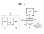
FIG. 2 is an explanatory diagram illustrating an outline of operation of thetemperature sensor 10. - As illustrated in
FIG. 2 , a temperature-voltage conversion circuit (TVC) 101 detects a chip temperature Tj, and generates two kinds of analog voltages (a reference voltage V1 and a reference voltage V2) corresponding to the chip temperature Tj. The reference voltages V1 and V2 are inputted into an A/D conversion unit (A/D) 102 in the following stage. The A/D conversion unit 102 converts the ratio (V1/V2) of the reference voltages V1 and V2 into a digital value, and outputs an A/D conversion result 103. Thecorrection operation unit 105 performs correcting operation based on the A/D conversion result 103, and outputs anoperation result 110. The correcting operation is performed using an approximate function of a characteristic function expressing the correspondence relation of the A/D conversion result 103 and temperature (the approximate function is also hereinafter called a "correction operation function"). The value of the coefficient of the correction operation function is calculated by thecoefficient calculation unit 104. For example, in the test process at the time of the mass production before shipment, thecoefficient calculation unit 104 calculates a coefficient based on the A/D conversion result 103 measured at a test temperature, and stores the calculated coefficient in thenonvolatile memory 502. At the time of the actual use after shipment, the information on the coefficient is transferred to thecorrection operation unit 105 from thenonvolatile memory 502. Thecorrection operation unit 105 performs the correcting operation using the correction operation function to which the transferred coefficient is applied, and outputs anoperation result 110 as a temperature sensor detecting temperature. - The following explains each functional block of the
temperature sensor 10 in detail. - The
sensor unit 100 comprises the temperature-voltage conversion circuit (TVC) 101 and the A/D conversion unit (A/D) 102. - The temperature-
voltage conversion circuit 101 outputs two reference voltages V1 and V2, which exhibit temperature dependence. -
FIG. 3 is a circuit diagram illustrating an example of the temperature-voltage conversion circuit 101. The temperature-voltage conversion circuit 101 illustrated inFIG. 3 is configured with two bipolar transistors of which the emitter areas are different. The temperature-voltage conversion circuit 101 outputs the reference voltage V1 with positive temperature dependence to temperature, and the reference voltage V2 with low temperature dependence. A parasitic bipolar transistor in the CMOS process is mainly utilized for the bipolar transistor.FIG. 3 illustrates, as an example, the case where a parasitic bipolar transistor of a vertical NPN type is used. As one means for changing the emitter area, plural bipolar transistors of the same kind may be coupled in parallel. - The principle of operation of the temperature-
voltage conversion circuit 101 is explained. InFIG. 3 , when the output voltage V2 of an operational amplifier is applied to a base (B1) of a parasitic bipolar transistor TB_NPN_1, and to bases of m parasitic bipolar transistors TB_NPN_m (m is an integer equal to or greater than one), a difference occurs in the current density of current which flows through an emitter of the parasitic bipolar transistor TB_NPN_1, and emitters of the parasitic bipolar transistors TB_NPN_m. Depending on the difference of the current density, a difference voltage ΔVBE between the base-emitter voltage of the parasitic bipolar transistor TB_NPN_1 and the base-emitter voltage of the parasitic bipolar transistor TB_NPN_m appears across both ends of a resistor R3. The difference voltage ΔVBE exhibits a positive temperature characteristic. The reference voltage V2 and the reference voltage V1 with a positive temperature characteristic are generated using the present difference voltage ΔVBE. The reference voltages V1 and V2 are expressed by Equation (1) and Equation (2) as follows. In the equations, k is the Boltzmann's constant, q is the charge of an electron, and T is temperature. The value of the reference voltage V2 expressed byEquation 2 is about 1.2v at a normal temperature.

- When the reference voltages V1 and V2 are expressed as a function of temperature T,
Equation 3 and Equation 4 are obtained as follows. Here, A, C, D, and E are constants.

- The A/
D conversion unit 102 inputs the reference voltages V1 and V2 outputted by the temperature-voltage conversion circuit 101 in an analog signal form, converts the ratio of the reference voltages V1 and V2 at a predetermined temperature into a digital signal of j bits (j is an integer equal to or greater than one), and outputs the A/D conversion result 103. The details of the A/D conversion unit 102 will be described later. - The
correction operation unit 105 performs correcting operation based on the A/D conversion result 103, and outputs theoperation result 110. As described above, the correcting operation is performed using a correction operation function, and the value of the coefficients of the correction operation function is calculated by thecoefficient calculation unit 104. - The correcting operation is explained in detail.
-
FIG. 4 is an explanatory diagram illustrating temperature characteristics of the reference voltages V1 and V2. As illustrated inFIG. 4 , taking temperatures τ1, τ2, τ3, and τ4 at an equal interval, the values of the reference voltages V1 and V2 at each temperature are assumed to be V11 - V14 and V21 - V24. The A/D conversion unit 102 converts a voltage ratio V11/V21 at temperature τ1, for example, into a digital value and outputs it as the A/D conversion result 103, and converts a voltage ratio V12/V22 at temperature τ2, for example, into a digital value, and outputs it as the A/D conversion result 103. Here, since the reference voltage V1 is a linearly increasing voltage in proportion to the temperature, a voltage difference between adjacent two of the four voltages V11, V12, V13, and V14 becomes equal. As compared with this, since the reference voltage V2 is a voltage which has nonlinear dependence on the temperature, a voltage difference between adjacent two of four voltages V12, V22, V23, and V24 is not equal. -
FIG. 5 is an explanatory diagram illustrating a relation between the voltage ratio V1/V2 as the input of the A/D conversion unit 102, and the A/D conversion result t as the output. Since the voltage difference between adjacent two of four voltages V21, V22, V23, and V24 of the reference voltage V2 at respective temperatures has nonlinear dependence on the temperature τ, as explained with reference toFIG. 4 , even if the temperature difference between adjacent two of the chip temperatures τ1, τ2, τ3, and τ4 is equal, the difference between adjacent two of the voltage ratios (V11/V21), (V12/V22), (V13/V23), and (V14/V24) is not equal. Therefore, even if the linearity of the A/D conversion unit is ideal as shown inFIG. 5 , the A/D conversion results t1, t2, t3, and t4 have nonlinear dependence on the temperature τ. The INL (integral nonlinearity) of the A/D conversion unit itself becomes also a factor which induces the nonlinear temperature dependence of the A/D conversion result. - Here, a consideration is given on what kind of value the input V1/V2 of the A/
D conversion unit 102 will converge at the absolute zero (T → 0). Since the reference voltage V1 is proportional to temperature as expressed byEquation 1 andEquation 3, the reference voltage V1 converges to "0" (zero) at the absolute zero as expressed by Equation 5 in the following. As expressed inEquation 2, the reference voltage V2 is a sum of a base-emitter voltage VBE (the first term) and a voltage proportional to temperature (the second term). Accordingly, at the absolute zero (T → 0), the first term of the reference voltage V2 converges to a band gap voltage and the second term converges to "0", and hence the reference voltage V2 converges to the band gap voltage (a constant C) at the absolute zero (T → 0), as expressed by Equation 6 in the following. Therefore, the voltage ratio V1/V2 converges to "0" at the absolute zero, as expressed by Equation 7 in the following. Finally, the above consideration results in a conclusion that the graph of the input-output characteristics of the AD conversion circuit passes the origin (0, 0), as illustrated inFIG. 5 . However, the temperature-voltage conversion circuit 101 and the A/D conversion unit 102 do not need to operate at the absolute zero, and any test at the absolute zero does not need to be performed in the test process before shipment. The fact that the graph passes theoretically the origin (0, 0) has been well derived from the physical characteristic of the reference voltage V1.


-
FIG. 6 is an explanatory diagram illustrating a characteristic function which expresses a correspondence relation of temperature T (τ) and the A/D conversion result t. As illustrated inFIG. 6 , the horizontal axis is the A/D conversion result t and the vertical axis is temperature T (K). In the figure, it is assumed that the temperatures T1, T2, T3, and T4 correspond to the A/D conversion results t1, t2, t3, and t4, respectively. The temperatures T1, T2, T3, and T4 correspond to temperatures τ1, τ2, τ3, and τ4 ofFIG. 4 , respectively. - The characteristic function illustrated in
FIG. 6 is expressed by Equation 8.
- In the equation, an - a0 are correction operation coefficients and t' is the A/D conversion result at a test temperature. As described above, since the limiting value of the A/D conversion result t converges to "0" at the absolute zero (T → 0), the characteristic function expressing the relation between the A/D conversion result t and the temperature sensor detecting temperature T after the correcting operation certainly passes the origin (0, 0).
- The characteristic function can also be expressed in terms of a fractional function (Equation 9) or an exponential function (Equation 10), for example. However, the present embodiment is explained by expressing the characteristic function in terms of Equation 8 as an example.


- As illustrated in
FIG. 6 , when using the characteristic function expressed by Equation 8, it is possible to compute the value of temperature T from the A/D conversion result t. Accordingly, in themicrocomputer 1, thecorrection operation unit 105 calculates the value of temperature T from the A/D conversion result t, using a correction operation function which approximates the characteristic function of a high order. The subsequent explanation is made on the assumption that the correction operation function is a second-order approximation function of the characteristic function. However, it is not restricted to the case, but when the temperature detection is performed with a greater accuracy, the characteristic function may be approximated with a function of a higher order than the second order (for example, a cubic function). -
FIG. 7 is an explanatory diagram illustrating a correction operation function when there are ideally no variations in a process. InFIG. 7 , a point marked by a circle is a corresponding point of the A/D conversion result t in the ideal state with no variations in the process and the chip temperature τ, and a curve 300 drawn by a dashed-dotted line is the correction operation function. The correction operation function 300 is a second-order approximation of the characteristic function, and is expressed by Equation 11.
- In the equation, a2 is a second-order correction operation coefficient, a1 is a first-order correction operation coefficient, and a0 is a zero-order correction operation coefficient. It is also assumed that the A/D conversion result t' at the test temperature is the A/D conversion result t1 at the test temperature τ1 as an example.
- When there is no process variation, the temperature sensor detecting temperature T and the actual temperature τ of a chip is substantially equal to a value which can be predicted by circuit simulation or the like; accordingly, the error of the chip temperature τ and the correcting operation result T is small. However, since an element characteristic exhibits variations by a process variation etc. as described above, the characteristic of the
temperature sensor 10 exhibits variations among chips; accordingly, it is likely that the characteristic function may differ for each chip. That is, it is likely that the correction operation coefficients an - a0 may differ for each chip. Accordingly, in themicrocomputer 1, thecoefficient calculation unit 104 calculates the correction operation coefficient an - a0 for each chip, based on the measurement result at the test temperature in the test process. -
FIG. 8 is an explanatory diagram illustrating an example of the calculation method of the correction operation coefficients an - a0.FIG. 8 illustrates the case of a second-order correction operation function as an example. In the figure, it is assumed that the A/D conversion result t is t1 at a test temperature τ1 and the A/D conversion result t is t2 at a test temperature τ2, in the test process before shipment. - Generally, in order to calculate an N-th order coefficient of an N-th order function, N+1 pieces of the measurement points are necessary. When one tries to calculate correction operation coefficients from two pieces of the measurement results (τ1, t1) and (τ2, t2) as illustrated in
FIG. 8 , it is possible to calculate the first-order correction operation coefficient a1 and the zero-order correction operation coefficient a0; however, it is not possible to calculate the second-order correction operation coefficient a2. In order to calculate the second-order correction operation coefficient a2, one more piece of the measurement result (τ3, t3) is necessary. Accordingly, inEmbodiment 1, paying attention to the point that the limiting value of the A/D conversion result t converges to "0" at the absolute zero (T → 0) theoretically, the N-th order correction operation coefficient is calculated, based on N+1 pieces of the A/D conversion results t which include N pieces of the measured values at N points of the test temperature and the theoretical value at the absolute zero. For example, in the case ofFIG. 8 , the correction operation coefficients a2 - a0 are obtained by solving the simultaneous equations which are derived by substituting the measurement results (τ1, t1), (τ2, t2), and the theoretical value (0, 0) into Equation 11 described above. Specifically, they are expressed by Equation 12 - Equation 14 as follows.


- Accordingly, all the three correction operation coefficients can be determined by performing the measurement at two points of the test temperature.
-
FIG. 9 is an explanatory diagram illustrating a correction operation function when there are variations in characteristics of themicrocomputer 1. InFIG. 9 , a circle indicates a corresponding point of the A/D conversion result t in the ideal state with no variations in the process and the actual chip temperature τ, and a curve attached with a reference symbol 301 is a correction operation function in the ideal state with no variations in the process. A triangle indicates a corresponding point of the measured value of the A/D conversion result t and actual chip temperature τ, and a curve attached with a reference symbol 302 is a correction operation function based on the measured value. - For example, when the value of the A/D conversion result t is (t1 - δt1) at a test temperature τ1 and the value of the A/D conversion result t is (t3 - δt3) at a test temperature τ3 in the test process of the
microcomputer 1, thecoefficient calculation unit 104 calculates correction operation coefficients a2_2, a1_2, and a0_2 by the method described above, using the measured values (τ1, t1 - δt1) and (τ3, t3 - δt3) and the theoretical value (0, 0). Then, thecorrection operation unit 105 performs calculation using a correction operation function 302 (a2_2 (t - t1)2 + a1_2(t - t1) + a0_2) to which the calculated correction operation coefficients a2_2, a1_2, and a0_2 are applied, and outputs the temperature detection result T. - In this way, by using the measured values, even when the A/D conversion result t to the chip temperature τ shifts from the ideal value due to process variations, the correction operation function corresponding to the characteristics of the chip can be determined. Accordingly, it is possible to reduce the error between the chip temperature τ and the temperature detection result T.
- In Equation 11 - Equation 14 described above, it is assumed that the A/D conversion result t' at the test temperature is the A/D conversion result t1 at the test temperature τ1. However, the present invention is not restricted to the case. Since Equation 11 is only an approximate function, an error may become large as the temperature departs from the test temperature. Therefore, it is preferable to determine the test temperature t', corresponding to the temperature range in which the accuracy enhancement of the temperature detection is desired. For example, when it is desired to enhance the temperature detection accuracy in the neighborhood of the temperature t2, the A/D conversion result t' of Equation 11 may be preferably set as the A/D conversion result t2 at the test temperature τ2.
-
FIG. 10 illustrates a comparative example in which the correction operation function is determined without using the theoretical value. InFIG. 10 , a circle indicates a corresponding point of the A/D conversion result t in the ideal state with no variations in the process and the actual chip temperature τ, and a curve attached with a reference symbol 301 is a correction operation function in the ideal state with no variations in the process. A triangle indicates a corresponding point of the measured value of the A/D conversion result t and the actual chip temperature τ, and a curve attached with a reference symbol 303 is a correction operation function based on the measured value. - For example, when the value of the A/D conversion result t is (t1 - δt1) at a test temperature τ1 and the value of the A/D conversion result t is (t3 - δt3) at a test temperature τ3, the correction operation coefficients which can be calculated from the measured value (τ1, t1 - δt1) and (τ3, t3 - δt3) without using the theoretical value (0, 0) are a first-order correction operation coefficient a1_3 and a zero-order correction operation coefficient a0_3. A second-order correction operation coefficient a2_3 cannot be computed because of the insufficient measurement points; therefore, a value predicted in advance in the simulation etc. is used for it. The
correction operation unit 105 performs calculation using a correction operation function 303 (a2_3 (t - t1)2 + a1_3 (t-t1) + a0_3) to which the correction operation coefficients a2_2, a1_2, and a0_2 are applied, and calculates the temperature detection result T. According to this, as illustrated inFIG. 10 , at the test temperatures τ1 and τ3, error from the correcting operation results T1 and T3 can be made small, however, as the point departs from the test temperature, the error between the chip temperature τ and the correcting operation result (temperature detection result) T increases, leading to insufficient enhancement of the accuracy of the temperature sensor. On the other hand, themicrocomputer 1 according to the present embodiment calculates the N-th correction operation coefficient from N pieces of the measured values, by utilizing the theoretical value at the absolute zero in addition to the measured value at the test temperature. Accordingly, only by testing at N points of temperature in the test process before shipment, an effect equivalent to the case of testing at N+1 points of temperature is obtained, and it becomes possible to correct the variations in thetemperature sensor 10 with a greater accuracy. - Next, the procedure of the correcting operation by the
microcomputer 1 is explained. -
FIG. 11 is a flow chart illustrating an example of calculation of the correction operation coefficients.FIG. 11 illustrates a process flow in calculating the correction operation coefficients in a test before product shipment. - For example, after installing the
microcomputer 1 as a measuring target in a tester, a test temperature is set at τ1 (S101) . When the temperature is stabilized, in response to the request for the temperature detection from theCPU 30 and others, thetemperature sensor 10 measures temperature and a measurement result (τ1, t1) is stored in the nonvolatile memory 502 (S102). Next, the tester sets the test temperature at τ2 (S103). Same as in Step S102, in response to the request for the temperature detection from theCPU 30 and others, thetemperature sensor 10 measures temperature and a measurement result (τ2, t2) is stored in the nonvolatile memory (S104). Then, the measurement results (τ1, t1) and (τ2, t2) stored in thenonvolatile memory 502 are transferred to the coefficient calculation unit 104 (S105). Thecoefficient calculation unit 104 calculates correction operation coefficients a2, a1, and a0 by the method described above using the transferred measurement results (τ1, t1) and (τ2, t2) and the theoretical value (0, 0) (S106). The calculated correction operation coefficients a2, a1, and a0 are stored in the nonvolatile memory 502 (S107). -
FIG. 12 is a flow chart illustrating an example of the correcting operation.FIG. 12 illustrates the process flow in performing the correcting operation at the time of the actual operation after the product shipment. - For example, in response to the request for the temperature detection from the
CPU 30 and others, thetemperature sensor 10 starts temperature measurement (S201). First, thetemperature sensor 10 reads the correction operation coefficients a2, a1, and a0 from the nonvolatile memory 502 (S202). The read correction operation coefficients a2, a1, and a0 are held at a register, for example, in thecorrection operation unit 105. Next, thesensor unit 100 performs temperature measurement and outputs the A/D conversion result t (S203). Thecorrection operation unit 105 inputs the A/D conversion result t, and performs the correcting operation using the correction operation coefficients a2, a1, and a0 held at the register (S204). Then, thecorrection operation unit 105 outputs the correcting operation result T as the temperature detection result, and the processing of the temperature measurement is terminated (S205). In the procedure, the order of Step S202 and Step S203 may be changed or Step S202 and Step S203 may be performed to the same timing. -
FIG. 13 illustrates a concrete configuration example of thecoefficient calculation unit 104 for realizing calculation of the correction operation coefficients. Thecoefficient calculation unit 104 is configured with an exclusive logic circuit which comprises subtractors 1040 - 1042, multipliers 1043 - 1048, anadder 1049,dividers coefficient calculation unit 104 also comprises a register, etc. (not shown) for holding the measured results (τ1, t1) and (τ2, t2), etc. which are transferred from thenonvolatile memory 502. -
FIG. 13 illustrates an configuration example of the logic circuit for realizing calculation by Equation 12 - Equation 14 described above. If the arithmetic function carried out by thecoefficient calculation unit 104 is realized by program execution by a microcomputer, when the chip temperature of themicrocomputer 1 becomes high, it is likely that the microcomputer which performs the calculation may fall into a runaway state, and that the correct operation result may no longer be obtained. However, realizing the arithmetic function with the exclusive logic circuit allows the stable operation even at a high temperature. -
FIG. 14 illustrates a concrete configuration example of thecorrection operation unit 105 for realizing the correcting operation. Thecorrection operation unit 105 is configured with an exclusive logic circuit which comprisesmultipliers adders -
FIG. 14 illustrates the configuration example of the logic circuit for realizing calculation using the second-order correction operation function described above (Equation 11). If the arithmetic function carried out by thecorrection operation unit 105 is realized by the program execution by a microcomputer, when the chip temperature of themicrocomputer 1 becomes high, it is likely that the microcomputer which performs calculation may fall into a runaway state, and that the correct operation result may no longer be obtained. However, realizing the arithmetic function with the exclusive logic circuit allows the stable operation even at a high temperature. -
FIG. 15 illustrates a concrete configuration example of the A/D conversion unit 102 for realizing the temperature measurement. The A/D conversion unit 102 comprises aninput stage 1020 and an A/D converter circuit (ADC) 1021 for performing A/D conversion. Theinput stage 1020 is provided with sampling capacitors C1 and C2 for holding input voltages, and switches. The A/D conversion unit 102 holds the reference voltages V1 and V2 in the sampling capacitors C1 and C2, and the A/D converter circuit 1021 samples the voltages held in the capacitors C1 and C2; thereby the A/D conversion unit 102 performs A/D conversion and outputs the A/D conversion result t. - When a potential difference is induced under the influence of a noise between the reference potential (ground voltage GND_TVC) of the temperature-
voltage conversion circuit 101 and the reference potential (ground voltage GND_ADC) of the A/D conversion unit 102, for example, the above-described precondition that the limiting value of the reference voltage V1 at the absolute zero (T → 0) is "0" no longer holds when seen from the ground voltage GND_ADC of the A/D converter circuit 1021. Accordingly, it is likely that the present fact may become an error factor of the temperature detection result T. In order to suppress the influence of a noise, at the time of the refresh operation of the sampling capacitors C1 and C2, the sampling capacitors are refreshed not by the ground voltage GND_ADC of the A/D converter circuit 1021 but by the ground voltage GND_TVC of the temperature-voltage conversion circuit 101. That is, thesensor unit 100 is laid out so that one end of the sampling capacitor is coupled to the node of the ground voltage GND_TVC and the other end of the sampling capacitor is coupled to the node of the ground voltage GND_TVC at the time of refreshment. -
FIG. 16 and FIG. 17 illustrate an example of the method of electrostatic shielding of the reference voltages V1 and V2. - In
FIG. 16 , ashielding wire 1011 is installed so as to be disposed in parallel with a signal line through which the reference voltage V1 is supplied, and ashielding wire 1012 is installed so as to be disposed in parallel with a signal line through which the reference voltage V2 is supplied. The shieldingwires voltage conversion circuit 101. Accordingly, the reference voltages V1 and V2 and the voltage of the shieldingwires wires - In
FIG. 17 , in addition to theshielding wires shielding wire 1013 is installed between the signal line through which the reference voltage V1 is supplied and the signal line through which the reference voltage V2 is supplied. The shieldingwires voltage conversion circuit 101. Accordingly, it is possible to reduce more the influence of a noise. It is also preferable to install shielding layers in the lower layer and upper layer of the wirings of V1 and V2 and the shielding wires 1011 - 1013. Accordingly, it is possible to reduce much more the influence of a noise. - It is clear from the above that, in the
microcomputer 1 according toEmbodiment 1, the theoretical value at the absolute zero is utilized in addition to the measured values at test temperatures; therefore, only by testing at N points of temperature, an effect equivalent to the case of testing at N+1 points of temperature is obtained. Accordingly, it is possible to attain the accuracy enhancement of the temperature measurement by thetemperature sensor 10, without further increase in the test process. - The above explanation has shown the method in which the calculation of the correction operation coefficients an - a0 is performed in the testing phase before shipping. However, it is not restricted to the method, and it is also preferable to adopt a method in which the calculation is performed at the time of the actual operation after shipment. For example, in the testing phase before shipment, the A/D conversion result t at the test temperature is stored in the
nonvolatile memory 502. Then, at the time of the actual operation after shipment, when the request for temperature measurement is made from theCPU 30 and others, thecoefficient calculation unit 104 reads the measurement result stored in thenonvolatile memory 502. Thecoefficient calculation unit 104 calculates the correction operation coefficients based on the measurement result read and the theoretical value, and transfers the calculation result to thecorrection operation unit 105. According to the method, it is possible to attain the accuracy enhancement of the temperature measurement as is the case with the above method, and it is possible to reduce the test time by omitting the processing of the coefficient calculation in the test process. The calculation of the correction operation coefficients by thecoefficient calculation unit 104 may not be performed every time the request for the temperature measurement from theCPU 30 and others is made. However, after themicrocomputer 1 starts and reset is canceled for example, thecoefficient calculation unit 104 may perform the calculation of the correction operation coefficients, and may hold the correction operation coefficients in a register, etc. of thecorrection operation unit 105. - Alternatively, without using the
coefficient calculation unit 104, the correction operation coefficients an - a0 may be calculated by a program execution device (for example, a PC etc.) such as a tester, in the testing phase before shipment, and the correction operation coefficients an - a0 calculated may be stored in thenonvolatile memory 502. The calculation method of the coefficients is the same as the one carried out by thecoefficient calculation unit 104. According to the method, without increasing the test temperatures as is the above case, it is possible to attain the accuracy enhancement of the temperature measurement of thetemperature sensor 10, and it is also possible to contribute to the reduction of the chip area of themicrocomputer 1 because thecoefficient calculation unit 104 becomes unnecessary. -
FIG. 18 is a block diagram illustrating an example of a microcomputer with a built-in temperature sensor, for performing data processing, etc. for a vehicle, according toEmbodiment 2. Although not limited in particular, themicrocomputer 2 illustrated inFIG. 18 is formed over a semiconductor substrate like single crystal silicon, by the well-known CMOS integrated circuit manufacturing technology. - As described above, in order to enhance the accuracy of the
temperature sensor 12, it is necessary to calculate the correction operation coefficients an - a0 and to perform the correcting operation. However, it is necessary to test operation of each functional block in the preceding stage and to check the existence or nonexistence of operation abnormality. Accordingly, for ease of the operation test of each functional block, themicrocomputer 2 according toEmbodiment 2 further comprises a functional block for the operation test, in addition to the function provided in themicrocomputer 1 according toEmbodiment 1. Specifically, themicrocomputer 2 further comprisesinput selectors output selector 114, and input-output terminals 61 - 65. InFIG. 18 , the same symbol is attached to the same component as themicrocomputer 1, and the detailed explanation thereof is omitted. - The
input selector 112 selects and outputs either the reference voltage V1 outputted by the temperature-voltage conversion circuit 101, or an external input voltage V1' inputted from the exterior via the terminal 63, in response to aninput selection signal 116 inputted from the exterior via theterminal 64. Theoutput voltage 117 is inputted into the A/D conversion unit 102. Theinput selector 113 selects and outputs either the reference voltage V2 outputted by the temperature-voltage conversion circuit 101, or an external input voltage V2' inputted from the exterior via the terminal 61, in response to aninput selection signal 115 inputted from the exterior via theterminal 62. Theoutput voltage 118 is inputted into the A/D conversion unit 102. - The
output selector 114 switches the output destination of the A/D conversion result 119, in response to anoutput selection signal 122 inputted from the exterior via theterminal 65. Specifically, either an input terminal of thecoefficient calculation unit 104 and thecorrection operation unit 105 or an output signal line of thecorrection operation unit 105 is selected as the output destination of the A/D conversion result 119. - The test method using the
input selectors output selector 114 is explained. - The test method of the A/
D conversion unit 102 is as follows. For example, the input selection signals 115 and 116 and theoutput selection signal 122 are set up so that theinput selectors output selector 114 outputs the A/D conversion result T bypassing thelogical unit 70. At this time, it is possible to determine whether the A/D conversion unit 102 is operating normally, by comparing the A/D conversion result t (119) outputted and the value of V1'/V2' predicted from the external input voltages V1' and V2'. - The test method of the logical unit 70 (the
coefficient calculation unit 104 and the correction operation unit 105) is as follows. For example, theoutput selection signal 122 is set up so that theoutput selector 114 may input the A/D conversion result 119 into thelogical unit 70. When it has been checked that the A/D conversion unit 102 is operating normally in the above-described test of the A/D conversion unit 102, it is possible to determine whether thecoefficient calculation unit 104 and thecorrection operation unit 105 are operating normally, by comparing the correcting operation result T and the predicted value of the operation result. - The test method of the temperature-
voltage conversion circuit 101 is as follows. The input selection signals 115 and 116 are set up so that theinput selectors D conversion unit 102 and thelogical unit 70 are operating normally in the above-described test of the A/D conversion unit 102 and thelogical unit 70, it is possible to determine whether the reference voltage V1 is outputted normally, by comparing the difference between the A/D conversion result 119 when the input voltage is the reference voltage V1 and the A/D conversion result 119 when the input voltage is the external input voltage V1'. The same applies to the reference voltage V2. Another test method is also preferable, in which theinput selector 112 is designed so as to output the reference voltage V1 to the terminal 63, and the reference voltage V1 is monitored outside the chip for determining the normal operation. The same applies to theinput selector 113. - It is also possible to utilize the
output selector 114 for uses other than the test. For example, when a high accuracy of the temperature detection is not needed fortemperature sensor 12, theoutput selection signal 122 is set up so that theoutput selector 114 may output the A/D conversion result T, bypassing thelogical unit 70. In this case, a switch signal is inputted, for example from theCPU 30 and others, instead of inputting the output selection signal 122 from the exterior. At this time, thelogical unit 70 is disabled and the output thereof is set to high impedance. Accordingly, although the accuracy enhancement of the temperature detection is not attained, the power consumption of themicrocomputer 1 can be reduced because thelogical unit 70 does not operate. - It is clear from the above that, in the
microcomputer 2 according toEmbodiment 2, as is the case withEmbodiment 1, it is possible to attain the accuracy enhancement of the temperature measurement without increasing the process of the test, and it is possible to easily perform the operation test of each functional block. -
FIG. 19 is a block diagram illustrating an example of a microcomputer with a built-in temperature sensor, for performing data processing, etc. for a vehicle, according toEmbodiment 3. Although not limited in particular, themicrocomputer 3 illustrated inFIG. 19 is formed over a semiconductor substrate like single crystal silicon, by the well-known CMOS integrated circuit manufacturing technology. - In addition to the function provided in the
microcomputer 2 according toEmbodiment 2, themicrocomputer 3 is provided with the function for switching the correction operation function depending on a temperature range. Specifically, themicrocomputer 3 further comprises acomparator 123 for determining the temperature range. InFIG. 19 , the same symbol is attached to the same component as themicrocomputers - As described above, in order to enhance the accuracy of the
temperature sensor 12, it is necessary to calculate the correction operation coefficients an - a0 and to perform the correcting operation. However, for the further reduction of the test cost, a consideration is given on the case where the test is performed at only one point of temperature τ1, and a correction operation function is used. In this case, by using two points, the measurement result (t1, τ1) and the theoretical value (0, 0), it is possible to calculate the first-order correction operation coefficient a1 and the zero-order correction operation coefficient a0 among three correction operation coefficients a2, a1, and a0 of the second-order function. However, it is not possible to calculate the second-order correction operation coefficient a2. Therefore, the second-order correction operation coefficient a2 uses a value predicted by the circuit simulation etc. Accordingly, as described with reference toFIG. 10 , it is likely that the temperature accuracy may deteriorate at a temperature departing from the test temperature τ1. In particular, the present influence will become still more notable when the specification of the operational temperature range demanded for the temperature sensor becomes a wide range. Accordingly, in themicrocomputer 3, the correcting operation is performed by switching the second-order correction operation coefficient a2 depending on the temperature range. -
FIG. 20 is an explanatory diagram illustrating an example of the correction operation function of which the correction operation coefficients are switched corresponding to a temperature range. InFIG. 20 , a circle indicates a corresponding point of the A/D conversion result t in the ideal state with no variations in the process and the actual chip temperature τ, and a triangle indicates a corresponding point of the A/D conversion result t of the measured value, and the actual chip temperature τ. The curve attached with areference symbol 401 is a correction operation function in the temperature range higher than the temperature corresponding to the A/D conversion result tp, and the curve attached with areference symbol 402 is a correction operation function in the temperature range lower than the temperature corresponding to the A/D conversion result tp. - As illustrated in
FIG. 20 , the correcting operation result T of thecorrection operation function 401 deviates from the measured value more significantly as the temperature becomes low, and the correcting operation result T of thecorrection operation function 402 deviates from the measured value more significantly as the temperature becomes high. Accordingly, with a border at the temperature corresponding to the A/D conversion result tp, on the high temperature side, thecorrection operation function 401 of a second-order correction operation coefficient a2_H is used, and on the low temperature side, thecorrection operation function 402 of a second-order correction operation coefficient a2_L is used. The values predicted by the circuit simulation etc. are used for the second-order correction operation coefficients a2_H and a2_L. According to the present device, even when the measurement points are reduced in the test process, it is possible to improve the accuracy of the temperature detection compared with the method described above with reference toFIG. 10 . - When the temperature range is separated into two temperature ranges: a range from a low temperature to the normal temperature and a range from the normal temperature to a high temperature, it is preferable to set the temperature corresponding to the A/D conversion result tp as the normal temperature (for example, 25°C) .
-
FIG. 21 illustrates a concrete configuration example of thecoefficient calculation unit 204 for realizing calculation of the correction operation coefficients ofFIG. 20 . Thecoefficient calculation unit 204 is configured with an exclusive logic circuit which comprises amultiplier 2041, anadder 2042, and adivider 2043. Thecoefficient calculation unit 204 also comprises a register etc. (not shown) to hold the measured result (τ1, t1) etc. transferred from thenonvolatile memory 502, for example.FIG. 21 illustrates a configuration example of the logic circuit for calculating the first-order correction operation coefficient a1 and the zero-order correction operation coefficient a0, with a fixed value for the second-order correction operation coefficient a2. The equations for calculating the first-order correction operation coefficient a1 and the zero-order correction operation coefficient a0 are obtained by substituting the measured result (τ1, t1) and the theoretical value (0, 0) into Equation 11 and solving the equation. They are expressed by Equation 15 and Equation 16 as follows.

-
FIG. 22 illustrates a concrete configuration example of thecorrection operation unit 205 for realizing the correcting operation ofFIG. 20 . Thecorrection operation unit 205 is configured with an exclusive logic circuit which comprisesmultipliers adders coefficient selector 2054. In the figure, the logic circuit for realizing the calculation using the second-order correction operation function described above (Equation 11) is configured with themultipliers adders multiplier 2050 is switched by thecoefficient selector 2054. Specifically, thecomparator 123 monitors the reference voltage V1 and the reference voltage V2 and reverses the logic of theswitch signal 124 for example, when the voltage ratio V1/V2 reaches a value corresponding to the A/D conversion result tp. Thecoefficient selector 2054 outputs either the correction operation coefficient a2_H or the correction operation coefficient a2_L to themultiplier 2050 in response to theswitch signal 124. - As described above, according to
Embodiment 3, the second-order correction operation coefficient a2 is switched depending on the temperature range when performing the correcting operation. Accordingly, even in a case where the number of points of the test temperature is reduced, it is possible to suppress deterioration of the accuracy of the temperature detection, and it is possible to attain further reduction of the test cost. Compared with the method of calculating three correction operation coefficients, the accuracy of the present method may be inferior due to the process variations of the reference voltages V1 and V2 and the influence of the characteristics of thecomparator 123. - The above-described explanation has been made on the method of switching the second-order correction operation coefficient a2 as an example for reducing the test cost. However, not restricted to this, it is also possible to use the function of switching the coefficient for another use. For example, it is also possible to output the A/D conversion result t as a test mode, without performing the correcting operation.
-
FIG. 23 illustrates a concrete configuration example of acorrection operation unit 305 for outputting the A/D conversion result t, without performing the correcting operation. Thecorrection operation unit 305 further comprisescoefficient selectors correction operation unit 205. Thecoefficient selector 2054 of the second-order correction operation coefficient a2 selects and outputs either "0" or "a2_x." Thecoefficient selector 2055 of the first-order correction operation coefficient a1 selects and outputs either "1" or "a1_x." Thecoefficient selector 2056 of the zero-order correction operation coefficient a0 selects and outputs either "t1" or "a0_x." Aselection signal 125 may be inputted, for example from theCPU 30 and others, or may be inputted via theoutput selector 114 from an external terminal. For example, when theselection signal 125 instructs a normal operation mode, thecoefficient selector 2054 outputs "a2_x", thecoefficient selector 2055 outputs "a1_x", and thecoefficient selector 2056 outputs "a0_x." Accordingly, thecorrection operation unit 305 outputs an operation result "T = a2_x(t - t1)2 + a1_x(t - t1) + a0_x." When theselection signal 125 instructs a test mode, thecoefficient selector 2054 outputs "0", thecoefficient selector 2055 outputs "1", and thecoefficient selector 2056 outputs "t1." Accordingly, thecorrection operation unit 305 outputs an operation result "T = t." As described above, according to thecorrection operation unit 305, even by performing the correcting operation, it is possible to fetch the A/D conversion result t, and to perform the operation test of the A/D conversion unit 102, etc. - As described above, the invention accomplished by the present inventors has been concretely explained based on various embodiments. However, it cannot be overemphasized that the present invention is not restricted to the embodiments, and it can be changed variously in the range which does not deviate from the gist.
- For example, in
Embodiment 1 throughEmbodiment 3, the method of using the second-order correction operation function has been explained; however it is not restricted to this but it is possible to use a correction operation function of the third or greater order. According to the method, although the test cost increases, the accuracy of the temperature detection can be improved more. The embodiments of the present invention have illustrated the case where thecoefficient calculation units correction operation units -
Embodiment 3 has illustrated the case where the function for switching the correction operation coefficient is applied to themicrocomputer 2 according toEmbodiment 2. However, it is not restricted to the case, but it is also possible to apply the function for switching to themicrocomputer 1 according toEmbodiment 1.
Claims (16)
- A semiconductor device comprising:a temperature sensor unit;a coefficient calculation unit operable to calculate up to the N-th order coefficient (N is an integer equal to or greater than one) of a correction function as an N-th order approximation of a characteristic function indicative of correspondence relation of temperature data measured by the temperature sensor unit and temperature, based on N+1 pieces of the temperature data including a theoretical value of the temperature data at a predetermined temperature in the characteristic function and N measured values of the temperature data measured by the temperature sensor unit at N points of temperature; anda correction operation unit operable to generate data including information on temperature, by performing calculation with the use of the correction function to which the coefficients calculated are applied, on the basis of temperature data outputted from the temperature sensor unit.
- The semiconductor device according to Claim 1,
wherein the temperature sensor unit generates the temperature data, on the basis of a first voltage of which the limiting value at the absolute zero is zero, and a second voltage of which the limiting value at the absolute zero is given by a constant other than zero,
wherein the predetermined temperature is the absolute zero, and
wherein the temperature data indicates a value corresponding to a ratio of the first voltage to the second voltage. - The semiconductor device according to Claim 2,
wherein the first voltage corresponds to a difference voltage of a base-emitter voltage of two bipolar transistors having mutually different emitter areas, and the second voltage corresponds to a forward voltage of a PN junction. - The semiconductor device according to Claim 2,
wherein the correction operation unit comprises an exclusive logic circuit. - The semiconductor device according to Claim 4,
wherein the coefficient calculation unit comprises an exclusive logic circuit. - The semiconductor device according to Claim 2,
wherein the correction operation unit performs the calculation, by switching the information on the coefficients depending on a temperature range. - The semiconductor device according to Claim 6,
wherein the correction operation unit switches the information on an N-th order coefficient among the information on the coefficients. - The semiconductor device according to Claim 6,
wherein the correction operation unit switches the information on the coefficient in a higher temperature range and a lower temperature range with reference to a predetermined temperature in the temperature range of required measurement temperature. - The semiconductor device according to Claim 2,
wherein the temperature sensor unit comprises:a temperature-voltage conversion circuit operable to output the first voltage and the second voltage; andan analog-to-digital conversion unit operable to input a voltage corresponding to the first voltage and a voltage corresponding to the second voltage, to sample the input voltage via each sampling capacitor, and to generate the temperature data. - The semiconductor device according to Claim 9,
wherein one end of the sampling capacitor is set to the same potential as a reference potential of the temperature-voltage conversion circuit, and
wherein the other end of the sampling capacitor is supplied with the first voltage or the second voltage at the time of sampling and set to the same potential as the reference potential of the temperature-voltage conversion circuit at the time of refreshment of the sampling capacitor. - The semiconductor device according to Claim 9,
wherein the temperature sensor unit further comprises:a first shielding wire operable to shield a signal line through which the first voltage is supplied; anda second shielding wire operable to shield a signal line through which the second voltage is supplied, andwherein the potential of the first shielding wire and the second shielding wire is set to the reference potential of the temperature-voltage conversion circuit. - The semiconductor device according to Claim 9,
wherein the temperature sensor unit further comprises:a first selection unit operable to switch from the first voltage and the second voltage to respective external input voltages in response to a selection signal, and to output to the analog-to-digital conversion unit. - The semiconductor device according to Claim 12,
wherein the temperature sensor unit further comprises:a second selection unit operable to switch an output destination of the temperature data generated by the analog-to-digital conversion unit, andwherein the second selection unit outputs the temperature data to either of an input signal line or an output signal line of the correction operation unit, in response to the selection signal inputted. - A data generation method for generating, with the use of a program execution device, data indicative of a coefficient of a correction function used by a semiconductor device which uses the correction function as an N-th order approximation (N is an integer equal to or greater than one) of a characteristic function indicative of the correspondence relation of temperature data measured by a temperature sensor and temperature, and which generates data including information on temperature from the temperature data measured by the temperature sensor,
wherein processing performed by the program execution device comprises a step of generating data indicative of an N-th order coefficient, based on N+1 pieces of the temperature data including a theoretical value of temperature data at a predetermined temperature in the characteristic function and N measured values of temperature data measured by the temperature sensor unit at N points of temperature. - The data generation method according to Claim 14,
wherein the temperature data indicates a value corresponding to a ratio of a second voltage of which the limiting value at the absolute zero is zero to a first voltage of which the limiting value at the absolute zero is given by a constant other than zero, and
wherein the predetermined temperature is the absolute zero. - The data generation method according to Claim 15,
wherein the first voltage corresponds to a forward voltage of a PN junction, and
wherein the second voltage corresponds to a difference voltage of a base-emitter voltage of two bipolar transistors having mutually different emitter areas.
Applications Claiming Priority (1)
| Application Number | Priority Date | Filing Date | Title |
|---|---|---|---|
| JP2011089080A JP5757772B2 (en) | 2011-04-13 | 2011-04-13 | Semiconductor device and data generation method |
Publications (3)
| Publication Number | Publication Date |
|---|---|
| EP2511682A2 true EP2511682A2 (en) | 2012-10-17 |
| EP2511682A3 EP2511682A3 (en) | 2015-12-30 |
| EP2511682B1 EP2511682B1 (en) | 2016-10-19 |
Family
ID=46044320
Family Applications (1)
| Application Number | Title | Priority Date | Filing Date |
|---|---|---|---|
| EP12160958.0A Active EP2511682B1 (en) | 2011-04-13 | 2012-03-23 | Semiconductor device and temperature data generation method |
Country Status (4)
| Country | Link |
|---|---|
| US (1) | US9360381B2 (en) |
| EP (1) | EP2511682B1 (en) |
| JP (1) | JP5757772B2 (en) |
| CN (1) | CN102735360B (en) |
Families Citing this family (8)
| Publication number | Priority date | Publication date | Assignee | Title |
|---|---|---|---|---|
| JP5878883B2 (en) * | 2013-02-26 | 2016-03-08 | 旭化成エレクトロニクス株式会社 | Method for correcting temperature characteristics of magnetic sensor |
| MX346018B (en) * | 2013-08-28 | 2017-03-02 | Nissan Motor | Sensor abnormality determining apparatus. |
| JP6373751B2 (en) * | 2014-12-25 | 2018-08-15 | ルネサスエレクトロニクス株式会社 | Semiconductor device |
| US10247616B2 (en) * | 2015-03-05 | 2019-04-02 | Renesas Electronics Corporation | Electronics device |
| JP6637374B2 (en) | 2016-04-27 | 2020-01-29 | ルネサスエレクトロニクス株式会社 | Semiconductor device and temperature sensor |
| US10007311B2 (en) * | 2016-08-15 | 2018-06-26 | Sandisk Technologies Llc | Adaptive temperature and memory parameter throttling |
| JP7078818B2 (en) | 2018-01-31 | 2022-06-01 | ソニーセミコンダクタソリューションズ株式会社 | Imaging device and calibration method |
| JP6732391B2 (en) * | 2018-06-12 | 2020-07-29 | 日本電信電話株式会社 | Calculating device, calculating method and program |
Citations (3)
| Publication number | Priority date | Publication date | Assignee | Title |
|---|---|---|---|---|
| JPH04225250A (en) | 1990-12-26 | 1992-08-14 | Fujitsu Ltd | Temperature measuring device |
| JP2001298160A (en) | 2000-04-17 | 2001-10-26 | Hitachi Ltd | Integrated circuit |
| JP2004134472A (en) | 2002-10-09 | 2004-04-30 | Nec Electronics Corp | Semiconductor device and method of measuring its internal temperature |
Family Cites Families (14)
| Publication number | Priority date | Publication date | Assignee | Title |
|---|---|---|---|---|
| AT369332B (en) * | 1980-08-06 | 1982-12-27 | Friedmann Kg Alex | TEMPERATURE CONTROL DEVICE FOR A CLIMATE OR HEATING SYSTEM, PREFERRED IN RAILWAY VEHICLES |
| US6456145B1 (en) * | 2000-09-28 | 2002-09-24 | Koninklijke Philips Electronics N.V. | Non-linear signal correction |
| WO2006030374A2 (en) | 2004-09-15 | 2006-03-23 | Koninklijke Philips Electronics N.V. | Digital temperature sensors and calibration thereof |
| GB0420486D0 (en) | 2004-09-15 | 2004-10-20 | Koninkl Philips Electronics Nv | Digital temperature sensors and calibration thereof |
| CN1879006B (en) * | 2004-10-07 | 2012-09-05 | 雅马哈株式会社 | Geomagnetic sensor and method for obtaining temperature coefficient of shift, temperature sensor and temperature sensor correction method |
| US7461972B2 (en) * | 2005-02-08 | 2008-12-09 | Altivera L.L.C. | One point calibration integrated temperature sensor for wireless radio frequency applications |
| JP2007193662A (en) * | 2006-01-20 | 2007-08-02 | Nsk Ltd | Bearing apparatus monitoring system |
| JP2007315052A (en) * | 2006-05-26 | 2007-12-06 | Nakanishi Eng:Kk | Folding door connecting device |
| US8303179B2 (en) * | 2006-06-03 | 2012-11-06 | Precision Linear Systems, Inc. | Temperature-sensing and transmitting assemblies, programmable temperature sensor units, and methods of making and using them |
| JP2008002853A (en) * | 2006-06-20 | 2008-01-10 | Omron Corp | Cold contact compensation circuit, correction method of cold contact compensation circuit, and temperature measuring device |
| US7556423B2 (en) * | 2007-01-08 | 2009-07-07 | Microchip Technology Incorporated | Temperature sensor bow compensation |
| JP2008249582A (en) * | 2007-03-30 | 2008-10-16 | Hitachi High-Tech Control Systems Corp | Function approximate temperature converter |
| JP4944006B2 (en) * | 2007-12-17 | 2012-05-30 | 株式会社山武 | Temperature sensor and temperature measurement method |
| US20100002747A1 (en) * | 2008-07-03 | 2010-01-07 | Bosch Enrique Company | System and method for n'th order digital piece-wise linear compensation of the variations with temperature of the non-linearities for high accuracy digital temperature sensors in an extended temperature range |
-
2011
- 2011-04-13 JP JP2011089080A patent/JP5757772B2/en active Active
-
2012
- 2012-03-23 EP EP12160958.0A patent/EP2511682B1/en active Active
- 2012-04-04 US US13/439,289 patent/US9360381B2/en active Active
- 2012-04-13 CN CN201210108048.5A patent/CN102735360B/en active Active
Patent Citations (3)
| Publication number | Priority date | Publication date | Assignee | Title |
|---|---|---|---|---|
| JPH04225250A (en) | 1990-12-26 | 1992-08-14 | Fujitsu Ltd | Temperature measuring device |
| JP2001298160A (en) | 2000-04-17 | 2001-10-26 | Hitachi Ltd | Integrated circuit |
| JP2004134472A (en) | 2002-10-09 | 2004-04-30 | Nec Electronics Corp | Semiconductor device and method of measuring its internal temperature |
Also Published As
| Publication number | Publication date |
|---|---|
| US9360381B2 (en) | 2016-06-07 |
| JP5757772B2 (en) | 2015-07-29 |
| US20120265473A1 (en) | 2012-10-18 |
| EP2511682B1 (en) | 2016-10-19 |
| EP2511682A3 (en) | 2015-12-30 |
| CN102735360A (en) | 2012-10-17 |
| JP2012220437A (en) | 2012-11-12 |
| CN102735360B (en) | 2017-03-22 |
Similar Documents
| Publication | Publication Date | Title |
|---|---|---|
| EP2511682B1 (en) | Semiconductor device and temperature data generation method | |
| CN107367336B (en) | System and method for temperature sensing | |
| US8290728B2 (en) | Method and apparatus for integrated circuit temperature control | |
| US9389126B2 (en) | Method and apparatus for low cost, high accuracy temperature sensor | |
| US20140092939A1 (en) | Thermal Sensor with Second-Order Temperature Curvature Correction | |
| TWI731065B (en) | Semiconductor device, temperature sensor and power supply voltage monitor | |
| US20160252409A1 (en) | Calibrated temperature sensing system | |
| JP2008513766A (en) | Digital temperature sensor and its calibration | |
| US11573134B2 (en) | Semiconductor device and test method of semiconductor device | |
| US20190013233A1 (en) | System reference with compensation of electrical and mechanical stress and life-time drift effects | |
| US7965128B2 (en) | Semiconductor device, and power source and processor provided with the same | |
| CN109791118B (en) | Measurement circuit for estimating resistance of resistive gas sensor | |
| US7882455B2 (en) | Circuit and method using distributed phase change elements for across-chip temperature profiling | |
| JP2011086742A (en) | Semiconductor device | |
| JP5315386B2 (en) | Temperature measurement circuit | |
| US10352775B2 (en) | Systems and methods for reducing temperature sensor reading variation due to device mismatch | |
| US9310261B2 (en) | Production-test die temperature measurement method and apparatus | |
| JP2000031823A (en) | A/d converter | |
| JP6942781B2 (en) | Temperature measurement method | |
| WO2016166901A1 (en) | Temperature measurement device | |
| US20240077366A1 (en) | Semiconductor device | |
| TW201323843A (en) | Temperature sensing devices | |
| CN117176086A (en) | Voltage compensation method and device, electronic equipment and storage medium | |
| JP2010136426A (en) | D/a converter and voltage source |
Legal Events
| Date | Code | Title | Description |
|---|---|---|---|
| PUAI | Public reference made under article 153(3) epc to a published international application that has entered the european phase |
Free format text: ORIGINAL CODE: 0009012 |
|
| AK | Designated contracting states |
Kind code of ref document: A2 Designated state(s): AL AT BE BG CH CY CZ DE DK EE ES FI FR GB GR HR HU IE IS IT LI LT LU LV MC MK MT NL NO PL PT RO RS SE SI SK SM TR |
|
| AX | Request for extension of the european patent |
Extension state: BA ME |
|
| RAP1 | Party data changed (applicant data changed or rights of an application transferred) |
Owner name: RENESAS ELECTRONICS CORPORATION |
|
| PUAL | Search report despatched |
Free format text: ORIGINAL CODE: 0009013 |
|
| AK | Designated contracting states |
Kind code of ref document: A3 Designated state(s): AL AT BE BG CH CY CZ DE DK EE ES FI FR GB GR HR HU IE IS IT LI LT LU LV MC MK MT NL NO PL PT RO RS SE SI SK SM TR |
|
| AX | Request for extension of the european patent |
Extension state: BA ME |
|
| RIC1 | Information provided on ipc code assigned before grant |
Ipc: G01K 15/00 20060101ALI20151123BHEP Ipc: G01K 7/01 20060101AFI20151123BHEP Ipc: G05F 3/30 20060101ALI20151123BHEP |
|
| GRAP | Despatch of communication of intention to grant a patent |
Free format text: ORIGINAL CODE: EPIDOSNIGR1 |
|
| 17P | Request for examination filed |
Effective date: 20160608 |
|
| RBV | Designated contracting states (corrected) |
Designated state(s): AL AT BE BG CH CY CZ DE DK EE ES FI FR GB GR HR HU IE IS IT LI LT LU LV MC MK MT NL NO PL PT RO RS SE SI SK SM TR |
|
| INTG | Intention to grant announced |
Effective date: 20160713 |
|
| GRAS | Grant fee paid |
Free format text: ORIGINAL CODE: EPIDOSNIGR3 |
|
| GRAA | (expected) grant |
Free format text: ORIGINAL CODE: 0009210 |
|
| AK | Designated contracting states |
Kind code of ref document: B1 Designated state(s): AL AT BE BG CH CY CZ DE DK EE ES FI FR GB GR HR HU IE IS IT LI LT LU LV MC MK MT NL NO PL PT RO RS SE SI SK SM TR |
|
| REG | Reference to a national code |
Ref country code: GB Ref legal event code: FG4D |
|
| REG | Reference to a national code |
Ref country code: CH Ref legal event code: EP |
|
| REG | Reference to a national code |
Ref country code: AT Ref legal event code: REF Ref document number: 838750 Country of ref document: AT Kind code of ref document: T Effective date: 20161115 |
|
| REG | Reference to a national code |
Ref country code: IE Ref legal event code: FG4D |
|
| REG | Reference to a national code |
Ref country code: DE Ref legal event code: R096 Ref document number: 602012024242 Country of ref document: DE |
|
| REG | Reference to a national code |
Ref country code: NL Ref legal event code: MP Effective date: 20161019 |
|
| REG | Reference to a national code |
Ref country code: LT Ref legal event code: MG4D |
|
| PG25 | Lapsed in a contracting state [announced via postgrant information from national office to epo] |
Ref country code: LV Free format text: LAPSE BECAUSE OF FAILURE TO SUBMIT A TRANSLATION OF THE DESCRIPTION OR TO PAY THE FEE WITHIN THE PRESCRIBED TIME-LIMIT Effective date: 20161019 |
|
| REG | Reference to a national code |
Ref country code: AT Ref legal event code: MK05 Ref document number: 838750 Country of ref document: AT Kind code of ref document: T Effective date: 20161019 |
|
| PG25 | Lapsed in a contracting state [announced via postgrant information from national office to epo] |
Ref country code: SE Free format text: LAPSE BECAUSE OF FAILURE TO SUBMIT A TRANSLATION OF THE DESCRIPTION OR TO PAY THE FEE WITHIN THE PRESCRIBED TIME-LIMIT Effective date: 20161019 Ref country code: NO Free format text: LAPSE BECAUSE OF FAILURE TO SUBMIT A TRANSLATION OF THE DESCRIPTION OR TO PAY THE FEE WITHIN THE PRESCRIBED TIME-LIMIT Effective date: 20170119 Ref country code: GR Free format text: LAPSE BECAUSE OF FAILURE TO SUBMIT A TRANSLATION OF THE DESCRIPTION OR TO PAY THE FEE WITHIN THE PRESCRIBED TIME-LIMIT Effective date: 20170120 Ref country code: LT Free format text: LAPSE BECAUSE OF FAILURE TO SUBMIT A TRANSLATION OF THE DESCRIPTION OR TO PAY THE FEE WITHIN THE PRESCRIBED TIME-LIMIT Effective date: 20161019 |
|
| PG25 | Lapsed in a contracting state [announced via postgrant information from national office to epo] |
Ref country code: FI Free format text: LAPSE BECAUSE OF FAILURE TO SUBMIT A TRANSLATION OF THE DESCRIPTION OR TO PAY THE FEE WITHIN THE PRESCRIBED TIME-LIMIT Effective date: 20161019 Ref country code: ES Free format text: LAPSE BECAUSE OF FAILURE TO SUBMIT A TRANSLATION OF THE DESCRIPTION OR TO PAY THE FEE WITHIN THE PRESCRIBED TIME-LIMIT Effective date: 20161019 Ref country code: HR Free format text: LAPSE BECAUSE OF FAILURE TO SUBMIT A TRANSLATION OF THE DESCRIPTION OR TO PAY THE FEE WITHIN THE PRESCRIBED TIME-LIMIT Effective date: 20161019 Ref country code: BE Free format text: LAPSE BECAUSE OF FAILURE TO SUBMIT A TRANSLATION OF THE DESCRIPTION OR TO PAY THE FEE WITHIN THE PRESCRIBED TIME-LIMIT Effective date: 20161019 Ref country code: NL Free format text: LAPSE BECAUSE OF FAILURE TO SUBMIT A TRANSLATION OF THE DESCRIPTION OR TO PAY THE FEE WITHIN THE PRESCRIBED TIME-LIMIT Effective date: 20161019 Ref country code: IS Free format text: LAPSE BECAUSE OF FAILURE TO SUBMIT A TRANSLATION OF THE DESCRIPTION OR TO PAY THE FEE WITHIN THE PRESCRIBED TIME-LIMIT Effective date: 20170219 Ref country code: PL Free format text: LAPSE BECAUSE OF FAILURE TO SUBMIT A TRANSLATION OF THE DESCRIPTION OR TO PAY THE FEE WITHIN THE PRESCRIBED TIME-LIMIT Effective date: 20161019 Ref country code: PT Free format text: LAPSE BECAUSE OF FAILURE TO SUBMIT A TRANSLATION OF THE DESCRIPTION OR TO PAY THE FEE WITHIN THE PRESCRIBED TIME-LIMIT Effective date: 20170220 Ref country code: RS Free format text: LAPSE BECAUSE OF FAILURE TO SUBMIT A TRANSLATION OF THE DESCRIPTION OR TO PAY THE FEE WITHIN THE PRESCRIBED TIME-LIMIT Effective date: 20161019 Ref country code: AT Free format text: LAPSE BECAUSE OF FAILURE TO SUBMIT A TRANSLATION OF THE DESCRIPTION OR TO PAY THE FEE WITHIN THE PRESCRIBED TIME-LIMIT Effective date: 20161019 |
|
| REG | Reference to a national code |
Ref country code: DE Ref legal event code: R097 Ref document number: 602012024242 Country of ref document: DE |
|
| PG25 | Lapsed in a contracting state [announced via postgrant information from national office to epo] |
Ref country code: RO Free format text: LAPSE BECAUSE OF FAILURE TO SUBMIT A TRANSLATION OF THE DESCRIPTION OR TO PAY THE FEE WITHIN THE PRESCRIBED TIME-LIMIT Effective date: 20161019 Ref country code: DK Free format text: LAPSE BECAUSE OF FAILURE TO SUBMIT A TRANSLATION OF THE DESCRIPTION OR TO PAY THE FEE WITHIN THE PRESCRIBED TIME-LIMIT Effective date: 20161019 Ref country code: EE Free format text: LAPSE BECAUSE OF FAILURE TO SUBMIT A TRANSLATION OF THE DESCRIPTION OR TO PAY THE FEE WITHIN THE PRESCRIBED TIME-LIMIT Effective date: 20161019 Ref country code: CZ Free format text: LAPSE BECAUSE OF FAILURE TO SUBMIT A TRANSLATION OF THE DESCRIPTION OR TO PAY THE FEE WITHIN THE PRESCRIBED TIME-LIMIT Effective date: 20161019 Ref country code: SK Free format text: LAPSE BECAUSE OF FAILURE TO SUBMIT A TRANSLATION OF THE DESCRIPTION OR TO PAY THE FEE WITHIN THE PRESCRIBED TIME-LIMIT Effective date: 20161019 |
|
| PLBE | No opposition filed within time limit |
Free format text: ORIGINAL CODE: 0009261 |
|
| STAA | Information on the status of an ep patent application or granted ep patent |
Free format text: STATUS: NO OPPOSITION FILED WITHIN TIME LIMIT |
|
| PG25 | Lapsed in a contracting state [announced via postgrant information from national office to epo] |
Ref country code: SM Free format text: LAPSE BECAUSE OF FAILURE TO SUBMIT A TRANSLATION OF THE DESCRIPTION OR TO PAY THE FEE WITHIN THE PRESCRIBED TIME-LIMIT Effective date: 20161019 Ref country code: BG Free format text: LAPSE BECAUSE OF FAILURE TO SUBMIT A TRANSLATION OF THE DESCRIPTION OR TO PAY THE FEE WITHIN THE PRESCRIBED TIME-LIMIT Effective date: 20170119 Ref country code: IT Free format text: LAPSE BECAUSE OF FAILURE TO SUBMIT A TRANSLATION OF THE DESCRIPTION OR TO PAY THE FEE WITHIN THE PRESCRIBED TIME-LIMIT Effective date: 20161019 |
|
| 26N | No opposition filed |
Effective date: 20170720 |
|
| REG | Reference to a national code |
Ref country code: CH Ref legal event code: PL |
|
| GBPC | Gb: european patent ceased through non-payment of renewal fee |
Effective date: 20170323 |
|
| PG25 | Lapsed in a contracting state [announced via postgrant information from national office to epo] |
Ref country code: SI Free format text: LAPSE BECAUSE OF FAILURE TO SUBMIT A TRANSLATION OF THE DESCRIPTION OR TO PAY THE FEE WITHIN THE PRESCRIBED TIME-LIMIT Effective date: 20161019 Ref country code: MC Free format text: LAPSE BECAUSE OF FAILURE TO SUBMIT A TRANSLATION OF THE DESCRIPTION OR TO PAY THE FEE WITHIN THE PRESCRIBED TIME-LIMIT Effective date: 20161019 |
|
| REG | Reference to a national code |
Ref country code: IE Ref legal event code: MM4A |
|
| REG | Reference to a national code |
Ref country code: FR Ref legal event code: ST Effective date: 20171130 |
|
| PG25 | Lapsed in a contracting state [announced via postgrant information from national office to epo] |
Ref country code: LU Free format text: LAPSE BECAUSE OF NON-PAYMENT OF DUE FEES Effective date: 20170323 Ref country code: FR Free format text: LAPSE BECAUSE OF NON-PAYMENT OF DUE FEES Effective date: 20170331 |
|
| PG25 | Lapsed in a contracting state [announced via postgrant information from national office to epo] |
Ref country code: LI Free format text: LAPSE BECAUSE OF NON-PAYMENT OF DUE FEES Effective date: 20170331 Ref country code: CH Free format text: LAPSE BECAUSE OF NON-PAYMENT OF DUE FEES Effective date: 20170331 Ref country code: GB Free format text: LAPSE BECAUSE OF NON-PAYMENT OF DUE FEES Effective date: 20170323 Ref country code: IE Free format text: LAPSE BECAUSE OF NON-PAYMENT OF DUE FEES Effective date: 20170323 |
|
| PG25 | Lapsed in a contracting state [announced via postgrant information from national office to epo] |
Ref country code: MT Free format text: LAPSE BECAUSE OF NON-PAYMENT OF DUE FEES Effective date: 20170323 |
|
| PG25 | Lapsed in a contracting state [announced via postgrant information from national office to epo] |
Ref country code: HU Free format text: LAPSE BECAUSE OF FAILURE TO SUBMIT A TRANSLATION OF THE DESCRIPTION OR TO PAY THE FEE WITHIN THE PRESCRIBED TIME-LIMIT; INVALID AB INITIO Effective date: 20120323 |
|
| PG25 | Lapsed in a contracting state [announced via postgrant information from national office to epo] |
Ref country code: CY Free format text: LAPSE BECAUSE OF NON-PAYMENT OF DUE FEES Effective date: 20161019 |
|
| PG25 | Lapsed in a contracting state [announced via postgrant information from national office to epo] |
Ref country code: MK Free format text: LAPSE BECAUSE OF FAILURE TO SUBMIT A TRANSLATION OF THE DESCRIPTION OR TO PAY THE FEE WITHIN THE PRESCRIBED TIME-LIMIT Effective date: 20161019 |
|
| PG25 | Lapsed in a contracting state [announced via postgrant information from national office to epo] |
Ref country code: TR Free format text: LAPSE BECAUSE OF FAILURE TO SUBMIT A TRANSLATION OF THE DESCRIPTION OR TO PAY THE FEE WITHIN THE PRESCRIBED TIME-LIMIT Effective date: 20161019 |
|
| PG25 | Lapsed in a contracting state [announced via postgrant information from national office to epo] |
Ref country code: AL Free format text: LAPSE BECAUSE OF FAILURE TO SUBMIT A TRANSLATION OF THE DESCRIPTION OR TO PAY THE FEE WITHIN THE PRESCRIBED TIME-LIMIT Effective date: 20161019 |
|
| PGFP | Annual fee paid to national office [announced via postgrant information from national office to epo] |
Ref country code: DE Payment date: 20240328 Year of fee payment: 13 |