EP2510397B1 - Method for manufacturing a multilayer structure with a lateral pattern for application in the xuv wavelength range, and bf and lmag structures manufactured according to this method - Google Patents
Method for manufacturing a multilayer structure with a lateral pattern for application in the xuv wavelength range, and bf and lmag structures manufactured according to this method Download PDFInfo
- Publication number
- EP2510397B1 EP2510397B1 EP10796182.3A EP10796182A EP2510397B1 EP 2510397 B1 EP2510397 B1 EP 2510397B1 EP 10796182 A EP10796182 A EP 10796182A EP 2510397 B1 EP2510397 B1 EP 2510397B1
- Authority
- EP
- European Patent Office
- Prior art keywords
- multilayer structure
- pattern
- lateral
- layers
- boron carbide
- Prior art date
- Legal status (The legal status is an assumption and is not a legal conclusion. Google has not performed a legal analysis and makes no representation as to the accuracy of the status listed.)
- Active
Links
- 238000000034 method Methods 0.000 title claims description 36
- 238000004519 manufacturing process Methods 0.000 title claims description 11
- 239000000463 material Substances 0.000 claims description 28
- INAHAJYZKVIDIZ-UHFFFAOYSA-N boron carbide Chemical compound B12B3B4C32B41 INAHAJYZKVIDIZ-UHFFFAOYSA-N 0.000 claims description 21
- 229910052580 B4C Inorganic materials 0.000 claims description 19
- 230000003287 optical effect Effects 0.000 claims description 11
- 229910052799 carbon Inorganic materials 0.000 claims description 10
- OKTJSMMVPCPJKN-UHFFFAOYSA-N Carbon Chemical compound [C] OKTJSMMVPCPJKN-UHFFFAOYSA-N 0.000 claims description 9
- PXHVJJICTQNCMI-UHFFFAOYSA-N Nickel Chemical compound [Ni] PXHVJJICTQNCMI-UHFFFAOYSA-N 0.000 claims description 9
- 239000011651 chromium Substances 0.000 claims description 9
- 229910052746 lanthanum Inorganic materials 0.000 claims description 9
- 230000000737 periodic effect Effects 0.000 claims description 9
- FZLIPJUXYLNCLC-UHFFFAOYSA-N lanthanum atom Chemical compound [La] FZLIPJUXYLNCLC-UHFFFAOYSA-N 0.000 claims description 8
- 238000001127 nanoimprint lithography Methods 0.000 claims description 8
- XEEYBQQBJWHFJM-UHFFFAOYSA-N Iron Chemical compound [Fe] XEEYBQQBJWHFJM-UHFFFAOYSA-N 0.000 claims description 6
- 229910052706 scandium Inorganic materials 0.000 claims description 6
- SIXSYDAISGFNSX-UHFFFAOYSA-N scandium atom Chemical compound [Sc] SIXSYDAISGFNSX-UHFFFAOYSA-N 0.000 claims description 6
- 229910052710 silicon Inorganic materials 0.000 claims description 6
- 229910052721 tungsten Inorganic materials 0.000 claims description 6
- XUIMIQQOPSSXEZ-UHFFFAOYSA-N Silicon Chemical compound [Si] XUIMIQQOPSSXEZ-UHFFFAOYSA-N 0.000 claims description 5
- 229910052804 chromium Inorganic materials 0.000 claims description 5
- 239000010703 silicon Substances 0.000 claims description 5
- WFKWXMTUELFFGS-UHFFFAOYSA-N tungsten Chemical compound [W] WFKWXMTUELFFGS-UHFFFAOYSA-N 0.000 claims description 5
- 239000010937 tungsten Substances 0.000 claims description 5
- VYZAMTAEIAYCRO-UHFFFAOYSA-N Chromium Chemical compound [Cr] VYZAMTAEIAYCRO-UHFFFAOYSA-N 0.000 claims description 4
- 238000001020 plasma etching Methods 0.000 claims description 4
- 230000007704 transition Effects 0.000 claims description 4
- ZOKXTWBITQBERF-UHFFFAOYSA-N Molybdenum Chemical compound [Mo] ZOKXTWBITQBERF-UHFFFAOYSA-N 0.000 claims description 3
- 238000005530 etching Methods 0.000 claims description 3
- 239000011733 molybdenum Substances 0.000 claims description 3
- 229910052759 nickel Inorganic materials 0.000 claims description 3
- ZOXJGFHDIHLPTG-UHFFFAOYSA-N Boron Chemical compound [B] ZOXJGFHDIHLPTG-UHFFFAOYSA-N 0.000 claims description 2
- 229910039444 MoC Inorganic materials 0.000 claims description 2
- 229910052796 boron Inorganic materials 0.000 claims description 2
- 230000005670 electromagnetic radiation Effects 0.000 claims description 2
- 238000009616 inductively coupled plasma Methods 0.000 claims description 2
- 229910052742 iron Inorganic materials 0.000 claims description 2
- HBVFXTAPOLSOPB-UHFFFAOYSA-N nickel vanadium Chemical compound [V].[Ni] HBVFXTAPOLSOPB-UHFFFAOYSA-N 0.000 claims description 2
- 229920003023 plastic Polymers 0.000 claims description 2
- 239000004033 plastic Substances 0.000 claims description 2
- 230000005855 radiation Effects 0.000 description 8
- VYPSYNLAJGMNEJ-UHFFFAOYSA-N Silicium dioxide Chemical compound O=[Si]=O VYPSYNLAJGMNEJ-UHFFFAOYSA-N 0.000 description 7
- 239000006185 dispersion Substances 0.000 description 7
- 238000002310 reflectometry Methods 0.000 description 5
- 230000007423 decrease Effects 0.000 description 4
- 238000010894 electron beam technology Methods 0.000 description 4
- 239000000758 substrate Substances 0.000 description 4
- 229910052681 coesite Inorganic materials 0.000 description 3
- 229910052906 cristobalite Inorganic materials 0.000 description 3
- 238000001459 lithography Methods 0.000 description 3
- 239000000377 silicon dioxide Substances 0.000 description 3
- 229910052682 stishovite Inorganic materials 0.000 description 3
- 229910052905 tridymite Inorganic materials 0.000 description 3
- 238000000609 electron-beam lithography Methods 0.000 description 2
- 238000000206 photolithography Methods 0.000 description 2
- 229920003229 poly(methyl methacrylate) Polymers 0.000 description 2
- 239000004926 polymethyl methacrylate Substances 0.000 description 2
- 241000446313 Lamella Species 0.000 description 1
- 238000003491 array Methods 0.000 description 1
- 230000004888 barrier function Effects 0.000 description 1
- 229910017052 cobalt Inorganic materials 0.000 description 1
- 239000010941 cobalt Substances 0.000 description 1
- GUTLYIVDDKVIGB-UHFFFAOYSA-N cobalt atom Chemical compound [Co] GUTLYIVDDKVIGB-UHFFFAOYSA-N 0.000 description 1
- 238000009792 diffusion process Methods 0.000 description 1
- 230000000694 effects Effects 0.000 description 1
- 238000000025 interference lithography Methods 0.000 description 1
- 229910052741 iridium Inorganic materials 0.000 description 1
- GKOZUEZYRPOHIO-UHFFFAOYSA-N iridium atom Chemical compound [Ir] GKOZUEZYRPOHIO-UHFFFAOYSA-N 0.000 description 1
- 229910052751 metal Inorganic materials 0.000 description 1
- 239000002184 metal Substances 0.000 description 1
- 229910052750 molybdenum Inorganic materials 0.000 description 1
- 238000005329 nanolithography Methods 0.000 description 1
- 239000002086 nanomaterial Substances 0.000 description 1
- 239000010453 quartz Substances 0.000 description 1
- 229910052702 rhenium Inorganic materials 0.000 description 1
- WUAPFZMCVAUBPE-UHFFFAOYSA-N rhenium atom Chemical compound [Re] WUAPFZMCVAUBPE-UHFFFAOYSA-N 0.000 description 1
- 239000004065 semiconductor Substances 0.000 description 1
- 239000002904 solvent Substances 0.000 description 1
- 238000004611 spectroscopical analysis Methods 0.000 description 1
- 238000001228 spectrum Methods 0.000 description 1
Images
Classifications
-
- B—PERFORMING OPERATIONS; TRANSPORTING
- B82—NANOTECHNOLOGY
- B82Y—SPECIFIC USES OR APPLICATIONS OF NANOSTRUCTURES; MEASUREMENT OR ANALYSIS OF NANOSTRUCTURES; MANUFACTURE OR TREATMENT OF NANOSTRUCTURES
- B82Y10/00—Nanotechnology for information processing, storage or transmission, e.g. quantum computing or single electron logic
-
- G—PHYSICS
- G02—OPTICS
- G02B—OPTICAL ELEMENTS, SYSTEMS OR APPARATUS
- G02B6/00—Light guides; Structural details of arrangements comprising light guides and other optical elements, e.g. couplings
- G02B6/24—Coupling light guides
- G02B6/26—Optical coupling means
- G02B6/34—Optical coupling means utilising prism or grating
-
- B—PERFORMING OPERATIONS; TRANSPORTING
- B82—NANOTECHNOLOGY
- B82Y—SPECIFIC USES OR APPLICATIONS OF NANOSTRUCTURES; MEASUREMENT OR ANALYSIS OF NANOSTRUCTURES; MANUFACTURE OR TREATMENT OF NANOSTRUCTURES
- B82Y40/00—Manufacture or treatment of nanostructures
-
- G—PHYSICS
- G02—OPTICS
- G02B—OPTICAL ELEMENTS, SYSTEMS OR APPARATUS
- G02B5/00—Optical elements other than lenses
- G02B5/08—Mirrors
- G02B5/0891—Ultraviolet [UV] mirrors
-
- G—PHYSICS
- G03—PHOTOGRAPHY; CINEMATOGRAPHY; ANALOGOUS TECHNIQUES USING WAVES OTHER THAN OPTICAL WAVES; ELECTROGRAPHY; HOLOGRAPHY
- G03F—PHOTOMECHANICAL PRODUCTION OF TEXTURED OR PATTERNED SURFACES, e.g. FOR PRINTING, FOR PROCESSING OF SEMICONDUCTOR DEVICES; MATERIALS THEREFOR; ORIGINALS THEREFOR; APPARATUS SPECIALLY ADAPTED THEREFOR
- G03F1/00—Originals for photomechanical production of textured or patterned surfaces, e.g., masks, photo-masks, reticles; Mask blanks or pellicles therefor; Containers specially adapted therefor; Preparation thereof
- G03F1/22—Masks or mask blanks for imaging by radiation of 100nm or shorter wavelength, e.g. X-ray masks, extreme ultraviolet [EUV] masks; Preparation thereof
- G03F1/24—Reflection masks; Preparation thereof
-
- G—PHYSICS
- G03—PHOTOGRAPHY; CINEMATOGRAPHY; ANALOGOUS TECHNIQUES USING WAVES OTHER THAN OPTICAL WAVES; ELECTROGRAPHY; HOLOGRAPHY
- G03F—PHOTOMECHANICAL PRODUCTION OF TEXTURED OR PATTERNED SURFACES, e.g. FOR PRINTING, FOR PROCESSING OF SEMICONDUCTOR DEVICES; MATERIALS THEREFOR; ORIGINALS THEREFOR; APPARATUS SPECIALLY ADAPTED THEREFOR
- G03F7/00—Photomechanical, e.g. photolithographic, production of textured or patterned surfaces, e.g. printing surfaces; Materials therefor, e.g. comprising photoresists; Apparatus specially adapted therefor
- G03F7/0002—Lithographic processes using patterning methods other than those involving the exposure to radiation, e.g. by stamping
-
- G—PHYSICS
- G21—NUCLEAR PHYSICS; NUCLEAR ENGINEERING
- G21K—TECHNIQUES FOR HANDLING PARTICLES OR IONISING RADIATION NOT OTHERWISE PROVIDED FOR; IRRADIATION DEVICES; GAMMA RAY OR X-RAY MICROSCOPES
- G21K1/00—Arrangements for handling particles or ionising radiation, e.g. focusing or moderating
- G21K1/06—Arrangements for handling particles or ionising radiation, e.g. focusing or moderating using diffraction, refraction or reflection, e.g. monochromators
- G21K1/062—Devices having a multilayer structure
Definitions
- the invention relates to a method for manufacturing a multilayer structure with a lateral pattern, in particular of an optical grating for application in an optical device for electromagnetic radiation with a wavelength in the wavelength range between 0.1 nm and 100 nm, comprising the steps of (i) providing a multilayer structure, and (ii) arranging a lateral pattern in the multilayer structure.
- the wavelength range between 0.1 nm and 10 ⁇ m comprises the hard X-ray range (wavelength between 0.1 nm and 10 nm) and the so-called XUV range (wavelength between 10 nm and 100 nm) which includes the range around a wavelength of 13.5 nm, referred to in literature as EUV radiation, as well as radiation in the soft X-ray range of the electromagnetic spectrum.
- Such an optical grating is for instance applied in the production of semiconductor circuits within the technical field of nanolithography.
- a particular example of such an optical grating is a so-called nano-Bragg-Fresnel (BF) structure, which forms a combination of a reflective optical element, a Bragg structure, and a diffractive optical element, a Fresnel structure.
- BF nano-Bragg-Fresnel
- LMAG lamellar multilayer amplitude grating
- BF structures and LMAG structures are known to manufacture according to per se known methods, such as electron beam (EB) lithography and deep ultraviolet (DUV) lithography.
- EB electron beam
- DUV deep ultraviolet
- DUV photolithography encounters problems of a fundamental nature at resolution levels in the structure to be manufactured of lower than 50 nm. Furthermore, DUV photolithography is only cost-effective in mass production on very large scale.
- Both methods have the drawback that the width of a lamella in a periodic lateral pattern amounts to a minimum of several hundred nanometres, while the period amounts to at least one ⁇ m.
- step (ii) of arranging the lateral pattern is performed by means of a method for nano-imprint lithography (NIL).
- NIL nano-imprint lithography
- the method for nano-imprint lithography for instance comprises at least the steps of (a) providing a stamp with a stamp pattern corresponding to the lateral three-dimensional pattern to be arranged, (b) applying a layer of a curable resist material to the multilayer structure, (c) arranging the stamp pattern, using the stamp, in the layer of resist material applied according to step (b), and curing this material, and (d) removing from the multilayer structure material not, or at least substantially not covered by resist material in accordance with the stamp pattern while forming the lateral three-dimensional pattern in the multilayer structure.
- a metal layer is deposited, prior to step (b) or following step (c), onto the multilayer structure which is flat or provided with a lateral pattern, and is subsequently applied as etching mask.
- the stamp to be provided according to the invention is for instance manufactured from Si or SiO 2 (quartz), in which the stamp pattern is arranged in accordance with a per se known method, for instance by means of electron beam lithography (EBL) or laser interference lithography.
- EBL electron beam lithography
- laser interference lithography for instance, by means of laser beam lithography (EBL) or laser interference lithography.
- the layer of resist material is removed using a solvent, and the multilayer structure provided with a three-dimensional pattern can be subjected to a subsequent process step.
- step (d) is for instance performed in accordance with a method for reactive ion etching (RIE), by means of an inductively coupled plasma (ICP) or according to a Bosch-type etching method.
- RIE reactive ion etching
- ICP inductively coupled plasma
- the lateral three-dimensional pattern to be formed in the multilayer structure in step (d) is given a parallel, widening wedge-shaped or narrowing wedge-shaped form from the surface of the multilayer structure.
- the resist material to be applied according to step (b) is preferably a UV-curable plastic which in cured state has a relatively low viscosity, for instance a polymethyl methacrylate (PMMA).
- PMMA polymethyl methacrylate
- step (ii) of arranging the lateral pattern is followed by step (iii) of applying a cover layer over the three-dimensional pattern.
- a BF structure may be manufactured according to the above described method, wherein the multilayer structure comprises a stack of layers of a first material from a first group comprising carbon (C) and silicon (Si) and of layers of a second material from a second group comprising the materials from the groups of transition elements from the fourth, fifth and sixth period of the periodic system of elements.
- the layers of the second material are selected from the group of transition elements comprising cobalt (Co), nickel (Ni), molybdenum (Mo), tungsten (W), rhenium (Re) and iridium (Ir).
- an optical element becomes available which can be applied for wavelength selection, focusing and collimation of radiation in the wavelength range between 0.1 nm and 100 nm with an efficiency which is not achievable with a prior art multilayer structure without lateral pattern.
- the invention relates to an LMAG structure manufacturing method, wherein the multilayer structure comprises a stack of layers of a first material from a first group comprising boron (B), boron carbide (B 4 C), carbon (C), silicon (Si) and scandium (Sc), and of layers of a second material from a second group comprising the materials from the groups of transition elements from the fourth, fifth and sixth period of the periodic system of elements.
- the multilayer structure comprises a stack of layers of a first material from a first group comprising boron (B), boron carbide (B 4 C), carbon (C), silicon (Si) and scandium (Sc), and of layers of a second material from a second group comprising the materials from the groups of transition elements from the fourth, fifth and sixth period of the periodic system of elements.
- the multilayer structure is selected from the group comprising stacks of layers of tungsten and silicon (W/Si), tungsten and boron carbide (W/B 4 C), molybdenum and boron carbide (Mo/B 4 C), lanthanum and boron carbide (La/B 4 C), chromium and carbon (Cr/C), iron and scandium (Fe/Sc), chromium and scandium (Cr/Sc), nickel and carbon (Ni/C) and nickel vanadium and carbon (NiV/C)
- a multilayer structure comprising a stack of layers of lanthanum and boron carbide (La/B 4 C) the layers of lanthanum and boron carbide are separated by layers of lanthanum boride (LaB), these layers functioning as diffusion barrier.
- LaB lanthanum boride
- an optical element becomes available which can be applied for wavelength selection, focusing and collimation of radiation in the wavelength range between 0.1 nm and 100 nm with an efficiency which is not achievable with a prior art multilayer structure without lateral pattern.
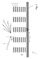
- FIG. 1 shows a schematic representation of the application of an LMAG structure 1 according to the invention as monochromator.
- LMAG structure 1 is formed by a substrate 2, for instance of SiO 2 , having thereon a multilayer structure of thin layers 3, 4 stacked on each other with a layer period d, wherein according to the above described method a periodic lateral structure is arranged with a lateral period D and a line width ⁇ D.
- a beam of XUV radiation (represented by arrow 5) with a wavelength ⁇ 0 is incident upon the surface of LMAG-structure 1 at an angle ⁇ 0 to the surface of LMAG-structure 1.
- the incident beam is diffracted by LMAG-structure 1 in an exiting zeroth order beam I 0 , first order beams I 1 , I -1 , second order beams I 2 , I -2 and higher order beams (not shown).
- an LMAG structure 1 according to the invention a monochromator can be provided which has a markedly lower dispersion (higher resolution) than with a flat, otherwise identical multilayer structure without lateral structure, wherein the reflectivity of the LMAG structure decreases to only slight extent compared to the reflectivity of the flat multilayer structure.
- a cover layer of SiO 2 with a thickness of 2 nm is applied to the structure (not shown in fig. 1 ).
Landscapes
- Physics & Mathematics (AREA)
- Engineering & Computer Science (AREA)
- General Physics & Mathematics (AREA)
- Nanotechnology (AREA)
- Chemical & Material Sciences (AREA)
- Crystallography & Structural Chemistry (AREA)
- Optics & Photonics (AREA)
- Condensed Matter Physics & Semiconductors (AREA)
- Manufacturing & Machinery (AREA)
- Spectroscopy & Molecular Physics (AREA)
- General Engineering & Computer Science (AREA)
- High Energy & Nuclear Physics (AREA)
- Mathematical Physics (AREA)
- Theoretical Computer Science (AREA)
- Diffracting Gratings Or Hologram Optical Elements (AREA)
- Shaping Of Tube Ends By Bending Or Straightening (AREA)
- Exposure Of Semiconductors, Excluding Electron Or Ion Beam Exposure (AREA)
Applications Claiming Priority (2)
| Application Number | Priority Date | Filing Date | Title |
|---|---|---|---|
| NL2003950A NL2003950C2 (nl) | 2009-12-11 | 2009-12-11 | Werkwijze voor het vervaardigen van een meerlagenstructuur met een lateraal patroon voor toepassing in het xuv-golflengtegebied en volgens deze werkwijze vervaardigde bt- en lmag-structuren. |
| PCT/NL2010/050832 WO2011071380A1 (en) | 2009-12-11 | 2010-12-08 | Method for manufacturing a multilayer structure with a lateral pattern for application in the xuv wavelength range, and bf and lmag structures manufactured according to this method |
Publications (2)
| Publication Number | Publication Date |
|---|---|
| EP2510397A1 EP2510397A1 (en) | 2012-10-17 |
| EP2510397B1 true EP2510397B1 (en) | 2015-01-14 |
Family
ID=42307776
Family Applications (1)
| Application Number | Title | Priority Date | Filing Date |
|---|---|---|---|
| EP10796182.3A Active EP2510397B1 (en) | 2009-12-11 | 2010-12-08 | Method for manufacturing a multilayer structure with a lateral pattern for application in the xuv wavelength range, and bf and lmag structures manufactured according to this method |
Country Status (6)
| Country | Link |
|---|---|
| US (1) | US20130220971A1 (zh) |
| EP (1) | EP2510397B1 (zh) |
| JP (1) | JP5782451B2 (zh) |
| CN (1) | CN102792222A (zh) |
| NL (1) | NL2003950C2 (zh) |
| WO (1) | WO2011071380A1 (zh) |
Families Citing this family (3)
| Publication number | Priority date | Publication date | Assignee | Title |
|---|---|---|---|---|
| NL2003950C2 (nl) * | 2009-12-11 | 2011-06-15 | Panalytical Bv | Werkwijze voor het vervaardigen van een meerlagenstructuur met een lateraal patroon voor toepassing in het xuv-golflengtegebied en volgens deze werkwijze vervaardigde bt- en lmag-structuren. |
| CN103018819B (zh) * | 2012-11-09 | 2014-05-21 | 浙江大学 | 基于纳米压印的高分子微纳光纤布拉格光栅制备方法 |
| KR101827814B1 (ko) * | 2016-04-15 | 2018-02-12 | 한국기계연구원 | 나노임프린트 방식을 이용한 3차원 구조체의 제조방법 |
Family Cites Families (18)
| Publication number | Priority date | Publication date | Assignee | Title |
|---|---|---|---|---|
| JPH0816720B2 (ja) * | 1992-04-21 | 1996-02-21 | 日本航空電子工業株式会社 | 軟x線多層膜反射鏡 |
| JPH07120607A (ja) * | 1993-10-22 | 1995-05-12 | Hitachi Ltd | 光学素子及びその製造方法 |
| JPH09326347A (ja) * | 1996-06-05 | 1997-12-16 | Hitachi Ltd | 微細パターン転写方法およびその装置 |
| GB2329484A (en) * | 1997-09-22 | 1999-03-24 | Northern Telecom Ltd | Writing Bragg reflection gratings in optical waveguides |
| JP4208447B2 (ja) * | 2001-09-26 | 2009-01-14 | 独立行政法人科学技術振興機構 | Sogを用いた室温ナノ−インプリント−リソグラフィー |
| JP4954498B2 (ja) * | 2004-06-01 | 2012-06-13 | 株式会社半導体エネルギー研究所 | 半導体装置の作製方法 |
| TWI366218B (en) * | 2004-06-01 | 2012-06-11 | Semiconductor Energy Lab | Method for manufacturing semiconductor device |
| KR100725037B1 (ko) * | 2005-01-21 | 2007-06-07 | 세메스 주식회사 | 반도체 플라즈마 처리 장치 및 방법 |
| WO2007057500A1 (en) * | 2005-11-18 | 2007-05-24 | Nanocomp Oy Ltd | Method of producing a diffraction grating element |
| US20070128875A1 (en) * | 2005-12-02 | 2007-06-07 | Jessing Jeffrey R | Dry etch release method for micro-electro-mechanical systems (MEMS) |
| JP3913765B1 (ja) * | 2005-12-28 | 2007-05-09 | 株式会社エンプラス | 偏光位相差板 |
| JP2008053666A (ja) * | 2006-08-28 | 2008-03-06 | Meisho Kiko Kk | パターン形成方法およびパターン形成体 |
| JP4996488B2 (ja) * | 2007-03-08 | 2012-08-08 | 東芝機械株式会社 | 微細パターン形成方法 |
| JP5092740B2 (ja) * | 2007-12-28 | 2012-12-05 | 住友電気工業株式会社 | 半導体素子の製造方法 |
| JP4453767B2 (ja) * | 2008-03-11 | 2010-04-21 | ソニー株式会社 | ホログラム基板の製造方法 |
| US8633052B2 (en) * | 2008-04-18 | 2014-01-21 | 1366 Technologies Inc. | Wedge imprint patterning of irregular surface |
| WO2010091907A1 (en) * | 2009-02-13 | 2010-08-19 | Asml Netherlands B.V. | Multilayer mirror and lithographic apparatus |
| NL2003950C2 (nl) * | 2009-12-11 | 2011-06-15 | Panalytical Bv | Werkwijze voor het vervaardigen van een meerlagenstructuur met een lateraal patroon voor toepassing in het xuv-golflengtegebied en volgens deze werkwijze vervaardigde bt- en lmag-structuren. |
-
2009
- 2009-12-11 NL NL2003950A patent/NL2003950C2/nl not_active IP Right Cessation
-
2010
- 2010-12-08 EP EP10796182.3A patent/EP2510397B1/en active Active
- 2010-12-08 US US13/515,127 patent/US20130220971A1/en not_active Abandoned
- 2010-12-08 CN CN2010800560817A patent/CN102792222A/zh active Pending
- 2010-12-08 WO PCT/NL2010/050832 patent/WO2011071380A1/en active Application Filing
- 2010-12-08 JP JP2012543036A patent/JP5782451B2/ja active Active
Also Published As
| Publication number | Publication date |
|---|---|
| NL2003950C2 (nl) | 2011-06-15 |
| WO2011071380A1 (en) | 2011-06-16 |
| JP5782451B2 (ja) | 2015-09-24 |
| CN102792222A (zh) | 2012-11-21 |
| US20130220971A1 (en) | 2013-08-29 |
| JP2013513940A (ja) | 2013-04-22 |
| EP2510397A1 (en) | 2012-10-17 |
Similar Documents
| Publication | Publication Date | Title |
|---|---|---|
| US9625811B2 (en) | Imprint lithography | |
| Jefimovs et al. | Zone-doubling technique to produce ultrahigh-resolution x-ray optics | |
| KR20050021980A (ko) | 다층 리소그래피 템플릿 및 그 제조 방법 | |
| Buitrago et al. | SnOx high-efficiency EUV interference lithography gratings towards the ultimate resolution in photolithography | |
| EP3631536B1 (en) | Height-modulated diffractive master plate and method of manufacturing thereof | |
| Fallica et al. | High-resolution grayscale patterning using extreme ultraviolet interference lithography | |
| EP2510397B1 (en) | Method for manufacturing a multilayer structure with a lateral pattern for application in the xuv wavelength range, and bf and lmag structures manufactured according to this method | |
| US7923177B2 (en) | Method for making a reflection lithographic mask and mask obtained by said method | |
| JP6277588B2 (ja) | パターン形成方法及びナノインプリント用テンプレートの製造方法 | |
| US20080044742A1 (en) | Method of correcting critical dimension in photomask and photomask having corrected critical dimension using the method | |
| Shi et al. | Scanning helium ion beam lithography | |
| EP2901212B1 (en) | Method for fabrication of nano-structures | |
| Naulleau et al. | Fabrication of high-efficiency multilayer-coated gratings for the EUV regime using e-beam patterned substrates | |
| Cherala et al. | Addressing nanoimprint lithography mix and match overlay using drop pattern compensation | |
| Van der Meer et al. | Improved resolution for soft-x-ray monochromatization using lamellar multilayer gratings | |
| Voronov et al. | Fabrication of x-ray gratings by direct write maskless lithography | |
| Mangat et al. | EUV mask fabrication with Cr absorber | |
| Wood et al. | Use of attenuated phase masks in extreme ultraviolet lithography | |
| US20130208254A1 (en) | Nano-photolithographic superlens device and method for fabricating same | |
| US9436091B2 (en) | Patterning method using surface plasmon | |
| Stein et al. | Diffractive x-ray optics using production fabrication methods | |
| Xie et al. | Towards high-order diffraction suppression using two-dimensional quasi-periodic gratings | |
| US20070052133A1 (en) | Methods for fabricating sub-resolution line space patterns | |
| Kato et al. | Fabrication of high aspect ratio nano gratings using SR lithography | |
| CN105807554B (zh) | 反射掩模及其制造方法 |
Legal Events
| Date | Code | Title | Description |
|---|---|---|---|
| PUAI | Public reference made under article 153(3) epc to a published international application that has entered the european phase |
Free format text: ORIGINAL CODE: 0009012 |
|
| 17P | Request for examination filed |
Effective date: 20120702 |
|
| AK | Designated contracting states |
Kind code of ref document: A1 Designated state(s): AL AT BE BG CH CY CZ DE DK EE ES FI FR GB GR HR HU IE IS IT LI LT LU LV MC MK MT NL NO PL PT RO RS SE SI SK SM TR |
|
| DAX | Request for extension of the european patent (deleted) | ||
| GRAP | Despatch of communication of intention to grant a patent |
Free format text: ORIGINAL CODE: EPIDOSNIGR1 |
|
| RIC1 | Information provided on ipc code assigned before grant |
Ipc: G02B 5/08 20060101ALN20140813BHEP Ipc: G03F 7/00 20060101AFI20140813BHEP Ipc: G03F 1/24 20120101ALI20140813BHEP Ipc: G21K 1/06 20060101ALN20140813BHEP |
|
| INTG | Intention to grant announced |
Effective date: 20140903 |
|
| GRAS | Grant fee paid |
Free format text: ORIGINAL CODE: EPIDOSNIGR3 |
|
| GRAA | (expected) grant |
Free format text: ORIGINAL CODE: 0009210 |
|
| AK | Designated contracting states |
Kind code of ref document: B1 Designated state(s): AL AT BE BG CH CY CZ DE DK EE ES FI FR GB GR HR HU IE IS IT LI LT LU LV MC MK MT NL NO PL PT RO RS SE SI SK SM TR |
|
| REG | Reference to a national code |
Ref country code: GB Ref legal event code: FG4D |
|
| REG | Reference to a national code |
Ref country code: CH Ref legal event code: EP |
|
| REG | Reference to a national code |
Ref country code: NL Ref legal event code: T3 Ref country code: IE Ref legal event code: FG4D |
|
| REG | Reference to a national code |
Ref country code: AT Ref legal event code: REF Ref document number: 707356 Country of ref document: AT Kind code of ref document: T Effective date: 20150215 |
|
| REG | Reference to a national code |
Ref country code: DE Ref legal event code: R096 Ref document number: 602010021859 Country of ref document: DE Effective date: 20150305 |
|
| REG | Reference to a national code |
Ref country code: AT Ref legal event code: MK05 Ref document number: 707356 Country of ref document: AT Kind code of ref document: T Effective date: 20150114 |
|
| REG | Reference to a national code |
Ref country code: LT Ref legal event code: MG4D |
|
| PG25 | Lapsed in a contracting state [announced via postgrant information from national office to epo] |
Ref country code: SE Free format text: LAPSE BECAUSE OF FAILURE TO SUBMIT A TRANSLATION OF THE DESCRIPTION OR TO PAY THE FEE WITHIN THE PRESCRIBED TIME-LIMIT Effective date: 20150114 Ref country code: HR Free format text: LAPSE BECAUSE OF FAILURE TO SUBMIT A TRANSLATION OF THE DESCRIPTION OR TO PAY THE FEE WITHIN THE PRESCRIBED TIME-LIMIT Effective date: 20150114 Ref country code: FI Free format text: LAPSE BECAUSE OF FAILURE TO SUBMIT A TRANSLATION OF THE DESCRIPTION OR TO PAY THE FEE WITHIN THE PRESCRIBED TIME-LIMIT Effective date: 20150114 Ref country code: NO Free format text: LAPSE BECAUSE OF FAILURE TO SUBMIT A TRANSLATION OF THE DESCRIPTION OR TO PAY THE FEE WITHIN THE PRESCRIBED TIME-LIMIT Effective date: 20150414 Ref country code: ES Free format text: LAPSE BECAUSE OF FAILURE TO SUBMIT A TRANSLATION OF THE DESCRIPTION OR TO PAY THE FEE WITHIN THE PRESCRIBED TIME-LIMIT Effective date: 20150114 Ref country code: BG Free format text: LAPSE BECAUSE OF FAILURE TO SUBMIT A TRANSLATION OF THE DESCRIPTION OR TO PAY THE FEE WITHIN THE PRESCRIBED TIME-LIMIT Effective date: 20150414 Ref country code: LT Free format text: LAPSE BECAUSE OF FAILURE TO SUBMIT A TRANSLATION OF THE DESCRIPTION OR TO PAY THE FEE WITHIN THE PRESCRIBED TIME-LIMIT Effective date: 20150114 |
|
| PG25 | Lapsed in a contracting state [announced via postgrant information from national office to epo] |
Ref country code: RS Free format text: LAPSE BECAUSE OF FAILURE TO SUBMIT A TRANSLATION OF THE DESCRIPTION OR TO PAY THE FEE WITHIN THE PRESCRIBED TIME-LIMIT Effective date: 20150114 Ref country code: IS Free format text: LAPSE BECAUSE OF FAILURE TO SUBMIT A TRANSLATION OF THE DESCRIPTION OR TO PAY THE FEE WITHIN THE PRESCRIBED TIME-LIMIT Effective date: 20150514 Ref country code: LV Free format text: LAPSE BECAUSE OF FAILURE TO SUBMIT A TRANSLATION OF THE DESCRIPTION OR TO PAY THE FEE WITHIN THE PRESCRIBED TIME-LIMIT Effective date: 20150114 Ref country code: GR Free format text: LAPSE BECAUSE OF FAILURE TO SUBMIT A TRANSLATION OF THE DESCRIPTION OR TO PAY THE FEE WITHIN THE PRESCRIBED TIME-LIMIT Effective date: 20150415 Ref country code: AT Free format text: LAPSE BECAUSE OF FAILURE TO SUBMIT A TRANSLATION OF THE DESCRIPTION OR TO PAY THE FEE WITHIN THE PRESCRIBED TIME-LIMIT Effective date: 20150114 Ref country code: PL Free format text: LAPSE BECAUSE OF FAILURE TO SUBMIT A TRANSLATION OF THE DESCRIPTION OR TO PAY THE FEE WITHIN THE PRESCRIBED TIME-LIMIT Effective date: 20150114 |
|
| REG | Reference to a national code |
Ref country code: DE Ref legal event code: R097 Ref document number: 602010021859 Country of ref document: DE |
|
| PG25 | Lapsed in a contracting state [announced via postgrant information from national office to epo] |
Ref country code: EE Free format text: LAPSE BECAUSE OF FAILURE TO SUBMIT A TRANSLATION OF THE DESCRIPTION OR TO PAY THE FEE WITHIN THE PRESCRIBED TIME-LIMIT Effective date: 20150114 Ref country code: CZ Free format text: LAPSE BECAUSE OF FAILURE TO SUBMIT A TRANSLATION OF THE DESCRIPTION OR TO PAY THE FEE WITHIN THE PRESCRIBED TIME-LIMIT Effective date: 20150114 Ref country code: DK Free format text: LAPSE BECAUSE OF FAILURE TO SUBMIT A TRANSLATION OF THE DESCRIPTION OR TO PAY THE FEE WITHIN THE PRESCRIBED TIME-LIMIT Effective date: 20150114 Ref country code: SK Free format text: LAPSE BECAUSE OF FAILURE TO SUBMIT A TRANSLATION OF THE DESCRIPTION OR TO PAY THE FEE WITHIN THE PRESCRIBED TIME-LIMIT Effective date: 20150114 Ref country code: RO Free format text: LAPSE BECAUSE OF FAILURE TO SUBMIT A TRANSLATION OF THE DESCRIPTION OR TO PAY THE FEE WITHIN THE PRESCRIBED TIME-LIMIT Effective date: 20150114 |
|
| PLBE | No opposition filed within time limit |
Free format text: ORIGINAL CODE: 0009261 |
|
| STAA | Information on the status of an ep patent application or granted ep patent |
Free format text: STATUS: NO OPPOSITION FILED WITHIN TIME LIMIT |
|
| REG | Reference to a national code |
Ref country code: FR Ref legal event code: PLFP Year of fee payment: 6 |
|
| 26N | No opposition filed |
Effective date: 20151015 |
|
| PG25 | Lapsed in a contracting state [announced via postgrant information from national office to epo] |
Ref country code: IT Free format text: LAPSE BECAUSE OF FAILURE TO SUBMIT A TRANSLATION OF THE DESCRIPTION OR TO PAY THE FEE WITHIN THE PRESCRIBED TIME-LIMIT Effective date: 20150114 |
|
| PG25 | Lapsed in a contracting state [announced via postgrant information from national office to epo] |
Ref country code: SI Free format text: LAPSE BECAUSE OF FAILURE TO SUBMIT A TRANSLATION OF THE DESCRIPTION OR TO PAY THE FEE WITHIN THE PRESCRIBED TIME-LIMIT Effective date: 20150114 |
|
| PG25 | Lapsed in a contracting state [announced via postgrant information from national office to epo] |
Ref country code: BE Free format text: LAPSE BECAUSE OF FAILURE TO SUBMIT A TRANSLATION OF THE DESCRIPTION OR TO PAY THE FEE WITHIN THE PRESCRIBED TIME-LIMIT Effective date: 20150114 |
|
| PG25 | Lapsed in a contracting state [announced via postgrant information from national office to epo] |
Ref country code: MC Free format text: LAPSE BECAUSE OF FAILURE TO SUBMIT A TRANSLATION OF THE DESCRIPTION OR TO PAY THE FEE WITHIN THE PRESCRIBED TIME-LIMIT Effective date: 20150114 Ref country code: LU Free format text: LAPSE BECAUSE OF FAILURE TO SUBMIT A TRANSLATION OF THE DESCRIPTION OR TO PAY THE FEE WITHIN THE PRESCRIBED TIME-LIMIT Effective date: 20151208 |
|
| REG | Reference to a national code |
Ref country code: CH Ref legal event code: PL |
|
| REG | Reference to a national code |
Ref country code: IE Ref legal event code: MM4A |
|
| PG25 | Lapsed in a contracting state [announced via postgrant information from national office to epo] |
Ref country code: CH Free format text: LAPSE BECAUSE OF NON-PAYMENT OF DUE FEES Effective date: 20151231 Ref country code: LI Free format text: LAPSE BECAUSE OF NON-PAYMENT OF DUE FEES Effective date: 20151231 Ref country code: IE Free format text: LAPSE BECAUSE OF NON-PAYMENT OF DUE FEES Effective date: 20151208 |
|
| REG | Reference to a national code |
Ref country code: FR Ref legal event code: PLFP Year of fee payment: 7 |
|
| PG25 | Lapsed in a contracting state [announced via postgrant information from national office to epo] |
Ref country code: SM Free format text: LAPSE BECAUSE OF FAILURE TO SUBMIT A TRANSLATION OF THE DESCRIPTION OR TO PAY THE FEE WITHIN THE PRESCRIBED TIME-LIMIT Effective date: 20150114 Ref country code: HU Free format text: LAPSE BECAUSE OF FAILURE TO SUBMIT A TRANSLATION OF THE DESCRIPTION OR TO PAY THE FEE WITHIN THE PRESCRIBED TIME-LIMIT; INVALID AB INITIO Effective date: 20101208 |
|
| PG25 | Lapsed in a contracting state [announced via postgrant information from national office to epo] |
Ref country code: CY Free format text: LAPSE BECAUSE OF FAILURE TO SUBMIT A TRANSLATION OF THE DESCRIPTION OR TO PAY THE FEE WITHIN THE PRESCRIBED TIME-LIMIT Effective date: 20150114 |
|
| PG25 | Lapsed in a contracting state [announced via postgrant information from national office to epo] |
Ref country code: MT Free format text: LAPSE BECAUSE OF FAILURE TO SUBMIT A TRANSLATION OF THE DESCRIPTION OR TO PAY THE FEE WITHIN THE PRESCRIBED TIME-LIMIT Effective date: 20150114 |
|
| REG | Reference to a national code |
Ref country code: FR Ref legal event code: PLFP Year of fee payment: 8 |
|
| PG25 | Lapsed in a contracting state [announced via postgrant information from national office to epo] |
Ref country code: PT Free format text: LAPSE BECAUSE OF FAILURE TO SUBMIT A TRANSLATION OF THE DESCRIPTION OR TO PAY THE FEE WITHIN THE PRESCRIBED TIME-LIMIT Effective date: 20150114 Ref country code: TR Free format text: LAPSE BECAUSE OF FAILURE TO SUBMIT A TRANSLATION OF THE DESCRIPTION OR TO PAY THE FEE WITHIN THE PRESCRIBED TIME-LIMIT Effective date: 20150114 Ref country code: MK Free format text: LAPSE BECAUSE OF FAILURE TO SUBMIT A TRANSLATION OF THE DESCRIPTION OR TO PAY THE FEE WITHIN THE PRESCRIBED TIME-LIMIT Effective date: 20150114 |
|
| PG25 | Lapsed in a contracting state [announced via postgrant information from national office to epo] |
Ref country code: AL Free format text: LAPSE BECAUSE OF FAILURE TO SUBMIT A TRANSLATION OF THE DESCRIPTION OR TO PAY THE FEE WITHIN THE PRESCRIBED TIME-LIMIT Effective date: 20150114 |
|
| REG | Reference to a national code |
Ref country code: FR Ref legal event code: PLFP Year of fee payment: 9 |
|
| REG | Reference to a national code |
Ref country code: NL Ref legal event code: HC Owner name: MALVERN PANALYTICAL B.V.; NL Free format text: DETAILS ASSIGNMENT: CHANGE OF OWNER(S), CHANGE OF OWNER(S) NAME; FORMER OWNER NAME: PANALYTICAL B.V. Effective date: 20190515 |
|
| REG | Reference to a national code |
Ref country code: DE Ref legal event code: R081 Ref document number: 602010021859 Country of ref document: DE Owner name: MALVERN PANALYTICAL B.V., NL Free format text: FORMER OWNER: PANALYTICAL B.V., ALMELO, NL |
|
| P01 | Opt-out of the competence of the unified patent court (upc) registered |
Effective date: 20230727 |
|
| PGFP | Annual fee paid to national office [announced via postgrant information from national office to epo] |
Ref country code: NL Payment date: 20231121 Year of fee payment: 14 |
|
| PGFP | Annual fee paid to national office [announced via postgrant information from national office to epo] |
Ref country code: GB Payment date: 20231121 Year of fee payment: 14 |
|
| PGFP | Annual fee paid to national office [announced via postgrant information from national office to epo] |
Ref country code: FR Payment date: 20231122 Year of fee payment: 14 Ref country code: DE Payment date: 20231121 Year of fee payment: 14 |