EP2509331A1 - Liquid crystal display device - Google Patents
Liquid crystal display device Download PDFInfo
- Publication number
- EP2509331A1 EP2509331A1 EP12163434A EP12163434A EP2509331A1 EP 2509331 A1 EP2509331 A1 EP 2509331A1 EP 12163434 A EP12163434 A EP 12163434A EP 12163434 A EP12163434 A EP 12163434A EP 2509331 A1 EP2509331 A1 EP 2509331A1
- Authority
- EP
- European Patent Office
- Prior art keywords
- liquid crystal
- substrate
- pixel
- crystal display
- electrodes
- Prior art date
- Legal status (The legal status is an assumption and is not a legal conclusion. Google has not performed a legal analysis and makes no representation as to the accuracy of the status listed.)
- Granted
Links
Images


Classifications
-
- G—PHYSICS
- G02—OPTICS
- G02F—OPTICAL DEVICES OR ARRANGEMENTS FOR THE CONTROL OF LIGHT BY MODIFICATION OF THE OPTICAL PROPERTIES OF THE MEDIA OF THE ELEMENTS INVOLVED THEREIN; NON-LINEAR OPTICS; FREQUENCY-CHANGING OF LIGHT; OPTICAL LOGIC ELEMENTS; OPTICAL ANALOGUE/DIGITAL CONVERTERS
- G02F1/00—Devices or arrangements for the control of the intensity, colour, phase, polarisation or direction of light arriving from an independent light source, e.g. switching, gating or modulating; Non-linear optics
- G02F1/01—Devices or arrangements for the control of the intensity, colour, phase, polarisation or direction of light arriving from an independent light source, e.g. switching, gating or modulating; Non-linear optics for the control of the intensity, phase, polarisation or colour
- G02F1/13—Devices or arrangements for the control of the intensity, colour, phase, polarisation or direction of light arriving from an independent light source, e.g. switching, gating or modulating; Non-linear optics for the control of the intensity, phase, polarisation or colour based on liquid crystals, e.g. single liquid crystal display cells
- G02F1/133—Constructional arrangements; Operation of liquid crystal cells; Circuit arrangements
- G02F1/1333—Constructional arrangements; Manufacturing methods
- G02F1/1347—Arrangement of liquid crystal layers or cells in which the final condition of one light beam is achieved by the addition of the effects of two or more layers or cells
- G02F1/13471—Arrangement of liquid crystal layers or cells in which the final condition of one light beam is achieved by the addition of the effects of two or more layers or cells in which all the liquid crystal cells or layers remain transparent, e.g. FLC, ECB, DAP, HAN, TN, STN, SBE-LC cells
-
- G—PHYSICS
- G02—OPTICS
- G02F—OPTICAL DEVICES OR ARRANGEMENTS FOR THE CONTROL OF LIGHT BY MODIFICATION OF THE OPTICAL PROPERTIES OF THE MEDIA OF THE ELEMENTS INVOLVED THEREIN; NON-LINEAR OPTICS; FREQUENCY-CHANGING OF LIGHT; OPTICAL LOGIC ELEMENTS; OPTICAL ANALOGUE/DIGITAL CONVERTERS
- G02F1/00—Devices or arrangements for the control of the intensity, colour, phase, polarisation or direction of light arriving from an independent light source, e.g. switching, gating or modulating; Non-linear optics
- G02F1/01—Devices or arrangements for the control of the intensity, colour, phase, polarisation or direction of light arriving from an independent light source, e.g. switching, gating or modulating; Non-linear optics for the control of the intensity, phase, polarisation or colour
- G02F1/13—Devices or arrangements for the control of the intensity, colour, phase, polarisation or direction of light arriving from an independent light source, e.g. switching, gating or modulating; Non-linear optics for the control of the intensity, phase, polarisation or colour based on liquid crystals, e.g. single liquid crystal display cells
- G02F1/133—Constructional arrangements; Operation of liquid crystal cells; Circuit arrangements
- G02F1/1333—Constructional arrangements; Manufacturing methods
- G02F1/1337—Surface-induced orientation of the liquid crystal molecules, e.g. by alignment layers
-
- H—ELECTRICITY
- H04—ELECTRIC COMMUNICATION TECHNIQUE
- H04N—PICTORIAL COMMUNICATION, e.g. TELEVISION
- H04N13/00—Stereoscopic video systems; Multi-view video systems; Details thereof
- H04N13/30—Image reproducers
- H04N13/302—Image reproducers for viewing without the aid of special glasses, i.e. using autostereoscopic displays
- H04N13/305—Image reproducers for viewing without the aid of special glasses, i.e. using autostereoscopic displays using lenticular lenses, e.g. arrangements of cylindrical lenses
-
- H—ELECTRICITY
- H04—ELECTRIC COMMUNICATION TECHNIQUE
- H04N—PICTORIAL COMMUNICATION, e.g. TELEVISION
- H04N13/00—Stereoscopic video systems; Multi-view video systems; Details thereof
- H04N13/30—Image reproducers
- H04N13/356—Image reproducers having separate monoscopic and stereoscopic modes
- H04N13/359—Switching between monoscopic and stereoscopic modes
-
- G—PHYSICS
- G02—OPTICS
- G02F—OPTICAL DEVICES OR ARRANGEMENTS FOR THE CONTROL OF LIGHT BY MODIFICATION OF THE OPTICAL PROPERTIES OF THE MEDIA OF THE ELEMENTS INVOLVED THEREIN; NON-LINEAR OPTICS; FREQUENCY-CHANGING OF LIGHT; OPTICAL LOGIC ELEMENTS; OPTICAL ANALOGUE/DIGITAL CONVERTERS
- G02F1/00—Devices or arrangements for the control of the intensity, colour, phase, polarisation or direction of light arriving from an independent light source, e.g. switching, gating or modulating; Non-linear optics
- G02F1/01—Devices or arrangements for the control of the intensity, colour, phase, polarisation or direction of light arriving from an independent light source, e.g. switching, gating or modulating; Non-linear optics for the control of the intensity, phase, polarisation or colour
- G02F1/13—Devices or arrangements for the control of the intensity, colour, phase, polarisation or direction of light arriving from an independent light source, e.g. switching, gating or modulating; Non-linear optics for the control of the intensity, phase, polarisation or colour based on liquid crystals, e.g. single liquid crystal display cells
- G02F1/133—Constructional arrangements; Operation of liquid crystal cells; Circuit arrangements
- G02F1/1333—Constructional arrangements; Manufacturing methods
- G02F1/1343—Electrodes
- G02F1/134309—Electrodes characterised by their geometrical arrangement
- G02F1/134381—Hybrid switching mode, i.e. for applying an electric field with components parallel and orthogonal to the substrates
-
- G—PHYSICS
- G02—OPTICS
- G02F—OPTICAL DEVICES OR ARRANGEMENTS FOR THE CONTROL OF LIGHT BY MODIFICATION OF THE OPTICAL PROPERTIES OF THE MEDIA OF THE ELEMENTS INVOLVED THEREIN; NON-LINEAR OPTICS; FREQUENCY-CHANGING OF LIGHT; OPTICAL LOGIC ELEMENTS; OPTICAL ANALOGUE/DIGITAL CONVERTERS
- G02F1/00—Devices or arrangements for the control of the intensity, colour, phase, polarisation or direction of light arriving from an independent light source, e.g. switching, gating or modulating; Non-linear optics
- G02F1/29—Devices or arrangements for the control of the intensity, colour, phase, polarisation or direction of light arriving from an independent light source, e.g. switching, gating or modulating; Non-linear optics for the control of the position or the direction of light beams, i.e. deflection
- G02F1/294—Variable focal length devices
Definitions
- the present invention relates to a display device, and more particularly, to a liquid crystal display device which allows a three-dimensional display using a liquid crystal lens.
- a liquid crystal display panel includes a TFT substrate having pixel electrodes and thin film transistors (TFT) arranged in a matrix, and a counter substrate that is located opposite the TFT substrate, having color filters positioned corresponding to the pixel electrodes on the TFT substrate.
- a liquid crystal is interposed between the TFT substrate and the counter substrate to form a display region.
- An image is formed by controlling light transmittance through liquid crystal molecules for each pixel. Since the liquid crystal is capable of controlling only polarization light, a light ray from a backlight is polarized by a lower polarizer before incidence to the TFT substrate, and controlled by a liquid crystal layer. It is further polarized by an upper polarizer again so as to be emitted to the outside. Therefore the light emitted from the liquid crystal display panel becomes polarization light.
- Japanese Patent No. 2862462 discloses the structure in which a liquid crystal lens has liquid crystal molecules interposed between an upper substrate and a lower substrate, upper substrate electrode patterns are formed in stripes on the upper substrate, and flat solid lower substrate electrode patterns are formed on the lower substrate so that the lens is formed through alignment of the liquid crystal molecules along the electric field generated by applying a voltage to both the upper and lower substrate electrode patterns.
- Japanese Unexamined Patent Application Publication (Translation of PCT Application) No. 2009-520231 discloses a liquid crystal lens that uses the electric field generated by a longitudinal electric field between the upper substrate electrode pattern and the lower substrate electrode pattern. Those upper and the lower substrate electrode patterns on the upper and lower substrates are similar, but an angle of 90° is formed therebetween through turning with each other. This makes it possible to make the lens to turn at 90° through the method of applying the voltage to the upper and lower substrate electrode patterns.
- the three-dimensional display may be performed both in horizontal and vertical modes.
- Figs. 10 to 13 schematically show a liquid crystal lens 10 and a 3D display using the liquid crystal lens 10.
- the terms "2D display” and “3D display” herein refer to the "two-dimensional display” and the "three-dimensional display”.
- the liquid crystal lens 10 has the same structure as the liquid crystal display element, which interposes the liquid crystal between two substrates which form electrodes. However, unlike the liquid crystal display for displaying purpose, it is not intended to be used for the control of polarization direction, and accordingly, no polarizer is used.
- Fig. 10 schematically shows the electrodes formed on the two substrates that interpose the liquid crystal.
- the electrode on the lower substrate 30 has a transversely long rectangular pattern as indicated by a solid line
- the electrode on the upper substrate 20 has a rectangular pattern as indicated by a dashed line.
- Rectangular boxes A and B denote electrode terminals that externally apply the voltage.
- the line which connects the electrode terminal to the electrode on the aforementioned substrate denotes a wiring.
- the electrode connected to the electrode terminal A may be designated as an electrode A
- the electrode connected to the electrode terminal B may be designated as an electrode B.
- each pattern on the upper and lower substrates is not limited, and those patterns may be reversed with respect to the upper and lower substrates. Since transmission of light is required, the transparent electrode such as ITO is used for forming at least the electrode as shown by the dashed line, which entirely covers the display portion.
- Arrow P1 shown in Fig. 10 denotes a rubbing direction on the lower substrate
- arrow P2 denotes a rubbing direction on the upper substrates.
- the interposed liquid crystal is aligned to have a part at a longer axis side directed toward the arrow direction when no voltage is applied.
- Fig. 11 is a sectional view taken along line Y-Y of Fig. 10 .
- the electrodes on the lower substrate 30 are set so that two pixels of a liquid crystal display panel 100 below the liquid crystal lens 10 are arranged between two electrodes. Actually, a pitch of the two pixels is not the same as the pitch of the electrodes. Those pitches are appropriately designed in accordance with an assumed viewing position.
- Fig. 11 illustrates a state where each voltage applied to the upper and lower electrodes is set to be the same, that is, no voltage is applied to the liquid crystal.
- the liquid crystal lens 10 is in an off-state. In this state, the liquid crystal is entirely in an alignment direction regulated through rubbing.
- the liquid crystal lens 10 as an optically uniform medium with respect to the transmitted light performs no action, while directly outputting the 2D image on the liquid crystal display panel 100.
- Fig. 12 illustrates a state where the voltage is applied to the upper and lower electrodes of the liquid crystal lens 10 so as to change the alignment direction of the liquid crystal, that is, the liquid crystal lens 10 is in an on-state.
- AC voltage is applied for preventing deterioration in the liquid crystal.
- the electrode on the upper substrate 20 is flat solid, and the lower electrodes locally exist. Therefore, the electric field applied to the liquid crystal is not uniform in the longitudinal and transverse directions.
- the liquid crystal molecules are also radially aligned as shown in the drawing.
- a liquid crystal molecule 50 exhibits a birefringent property.
- Polarization light of transmitted light has the component in the longitudinal direction (longer axis direction) of the molecule brought into extraordinary light with high refractive index.
- the component orthogonal to the one in the longitudinal direction of the molecule is brought into ordinary light with lower refractive index than that of the extraordinary light.
- the intervening angle may be obtained through resolution into the extraordinary light component and the ordinary light component in the same manner as vector resolution.
- the birefringent property aligns the liquid crystal as shown in Fig. 12 .
- a polarization direction 40 of the incident light that is, the light emitted from the liquid crystal display panel 100 is substantially parallel to the rubbing direction on the liquid crystal lens 10
- the ratio between the portion with high refractive index (extraordinary light) and the portion with low refractive index upon passage of the incident light through the liquid crystal lens 10 varies by location.
- the longer axis direction of the liquid crystal molecule 50 is in line with the rubbing direction which determines an initial alignment of the liquid crystal.
- a dashed line representative of an interface of a convex lens 11 schematically shows the interface between the portion with high refractive index and the portion with low refractive index.
- the same effect as the one derived from the convex lens is obtained in the liquid crystal.
- each of codes "r", “g” and “b” of the first pixel 200 and the second pixel 300 denotes a "red sub-pixel", a "green sub-pixel” and a “blue sub-pixel”, respectively, common to all the pixels.
- the light from the first pixel 200 and the light from the second pixel 300 may be guided to the right eye and the left eye of a viewer, respectively. This allows the viewer to recognize the 3D image.
- Fig. 13 is a plan view representing a relationship between pixels of the liquid crystal display panel 100 for right and left eyes and low electrode patterns 31 of the liquid crystal lens.
- the pixels for the right eye are designated as A1 to A4, and those for the left eye are designated as B1 to B4.
- Fig. 14 illustrates the liquid crystal lens 10 with respect to the pattern configuration of the lower substrate electrode patterns 31 and the rubbing direction. Referring to Fig. 14 , both the rubbing direction P1 on the upper substrate and the rubbing direction P2 on the lower direction are transverse. The polarization direction 40 of emission from the liquid crystal display panel is transverse as well.
- Fig. 15 is a sectional view of the liquid crystal lens 10 shown in Fig. 14 in a state where no voltage is applied between the upper substrate 20 and the lower substrate 30.
- Fig. 16 is a sectional view of the liquid crystal lens 10 in the state where the voltage is applied between the upper substrate 20 and the lower substrate 30.
- a pair of polarized sunglasses as shown in Fig. 17 may be used when fishing on the seashore, for example, for preventing difficulty in viewing scenery owing to incidence of light reflected from the water surface.
- the transmission polarization axis of the polarized sunglasses is in a vertical direction as shown in Fig. 17 .
- the emission polarization axis of the liquid crystal lens as shown in Figs. 14 to 16 is transverse.
- the light ray that has passed through the liquid crystal lens may fail to pass through the polarized sunglasses. Accordingly, the viewer cannot see the image on the liquid crystal display device provided with the liquid crystal lens.
- the polarization axis of the light ray that has passed through the liquid crystal lens as shown in Figs. 14 to 16 is in an arrowed direction B shown in Fig. 18 . Since the transmission polarization axis of the polarized sunglasses is vertical, the light that has passed through the liquid crystal lens shown in Figs. 14 to 16 cannot be visually recognized through the polarized sunglasses. If the polarization axis of the light which has passed through the liquid crystal lens is in an arrowed direction A, the emitted light is allowed to pass through the polarized sunglasses.
- Figs. 19 to 21 show the liquid crystal lens having the polarization axis of the light emitted from the liquid crystal lens vertically directed.
- Fig. 19 illustrates the lower substrate electrode patterns 31 and the rubbing direction on the liquid crystal lens 10. Referring to Fig. 19 , the rubbing direction P1 on the lower substrate and the rubbing direction P2 on the upper direction are vertical. The polarization axis of the light emitted from the liquid crystal display panel is also in the vertical direction. Accordingly, the light that has passed through the liquid crystal lens 10 as shown in Figs. 19 to 21 may be visually recognized through the polarized sunglasses.
- Fig. 20 shows the state where no voltage is applied between the upper substrate 20 and the lower substrate 30 of the liquid crystal lens 10 shown in Fig. 19 .
- Fig. 21 shows the state where the voltage is applied between those substrates.
- the liquid crystal molecules are not modulated, the light emitted from the liquid crystal display panel 100 directly passes through the liquid crystal lens 10.
- the voltage is applied between the upper substrate 20 and the lower substrate 30 to form the liquid crystal lens, which enables the 3D display.
- the polarization axis of the light passing through the liquid crystal lens 10 is in the vertical direction, which may be visually recognized through the polarized sunglasses.
- the present invention provides the liquid crystal display device with the liquid crystal lens that enables 3D display, which allows clear visualization of the image from the liquid crystal display device using the polarized sunglasses.
- the function capable of selectively displaying in the portrait mode (vertical display) and the landscape mode (horizontal display) has been added like the mobile phone.
- the 3D panel is required to have the function for selecting the display between the vertical and the horizontal modes.
- Fig. 22 shows an example of generally employed art which allows the liquid crystal lens 10 to select the display in the vertical and horizontal modes.
- the solid line indicates the lower substrate electrode patterns 31
- the dashed line indicates the upper substrate electrode patterns 21.
- Each of the upper substrate 20 and the lower substrate 30 is formed of narrow electrodes each as the local electrode, and wide electrodes so as to be solid corresponding to the narrow electrodes on the counter substrate.
- Codes "A”, “B”, “C” and “D" refer to the terminal electrodes for application of voltage to the respective electrode patterns, and also refer to corresponding electrodes.
- Figs. 23 and 24 are sectional views each showing formation of the transversely extending cylindrical liquid crystal lens 10 shown in Fig. 22 .
- the consequence substantially the same as the one described referring to Figs. 11 and 12 occurs so as to provide the function of the liquid crystal lens 10.
- the state shown in Figs. 23 and 24 is different from the one shown in Figs. 11 and 12 in that a transverse electric field is generated between the electrodes A and C as indicated by Fig. 24 .
- This transverse electric field is substantially in the same direction as the rubbing direction, thus giving no fatal impact on the liquid crystal alignment and the lens effect.
- Figs. 25 and 26 are sectional views each taken along line X-X of Fig. 22 .
- Fig. 25 shows the state where no voltage is applied to the liquid crystal for 2D display.
- the liquid crystal molecules 50 each shown as a circle in the drawing indicates that the longer axis is longitudinally directed with respect to the upper electrode, that is, in the vertical direction with respect to a plane of the drawing.
- Fig. 26 shows the state where the voltage is applied so that the electric field is generated between the electrode B and the other electrodes A, C and D on the upper substrate 20.
- the liquid crystal is aligned again along the radial electric field directed toward C from B so as to form a downward convex lens shape.
- the transverse electric field is simultaneously generated between the electrodes B and D on the upper substrate 20.
- the liquid crystal is also aligned again along this electric field.
- the present invention provides a liquid crystal display device having a liquid crystal lens on a liquid crystal display panel.
- the present invention allows the liquid crystal display device to visualize the 3D image regardless of using the polarized sunglasses, and further allows the selective 3D display between vertical and horizontal modes.
- rubbing direction is used to refer to the direction of the liquid crystal molecules for initial alignment.
- the present invention may be applied to the optical alignment process for the initial alignment of the liquid crystal.
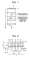
- Fig. 1 is a plan view illustrating the electrode structure of the liquid crystal lens 10 according to Example 1, and the rubbing directions on the upper substrate 20 and the lower substrate 30.
- the electrode structure shown in Fig. 1 is the same as the electrode structure shown in Fig. 10 , and the explanation thereof, thus will be omitted.
- the structure shown in Fig. 1 is different from the one shown in Fig. 10 in the rubbing direction on the upper substrate 20.
- the rubbing direction on the lower substrate 30 is vertical with respect to the extending direction of the lower substrate electrode pattern 31 in the same manner as the structure shown in Fig. 10 .
- the rubbing direction on the upper substrate 20 is the same as the extending direction of the lower substrate electrode pattern 31. Therefore, the initial alignment of the liquid crystal molecules interposed between the upper substrate 20 and the lower substrate 30 is twisted.
- Fig. 2 is a sectional view of the liquid crystal lens 10 shown in Fig. 1 taken along line Y-Y.
- the structure as illustrated in Fig. 2 is the same as the structure shown in Fig. 11 except the rubbing direction on the upper substrate 20 and the initial alignment of the liquid crystal molecules 50, and detailed explanations of the structure will be omitted.
- the polarization axis of the light emitted from the liquid crystal display panel 100 is in the same transverse direction as the rubbing direction on the lower substrate 30 of the liquid crystal lens 10. Meanwhile, the rubbing direction on the upper substrate 20 is at a right angle with the rubbing direction on the lower substrate 30.
- Fig. 2 represents the state of the aforementioned structure where no voltage is applied between the upper substrate 20 and the lower substrate 30.
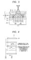
- Fig. 3 represents the same structure shown in Fig. 2 in the state where the voltage is applied between the upper substrate 20 and the lower substrate 30 to form the liquid crystal lens 10 like the convex lens.
- the liquid crystal lens 10 extends vertically with respect to the plane of the drawing to form a cylindrical lens.
- the application of the aforementioned lens for the 3D display allows provision of sufficiently practical images although the resultant brightness is lowered to a certain extent. This is thought to be caused by the residual TN effect, around the center of the lens 10, having the rotary polarization component left to a degree that keeps the viewer nearly imperceptible to the brightness deterioration.
- the change axis of polarization from the liquid crystal lens 10 may be brought to be in line with the polarization axis of polarized sunglasses 400.
- the image on the liquid crystal display device may be recognized even when the polarized sunglasses 400 are used.
- Fig. 4 is a plan view of Example 2 according to the present invention, which is the same as Example 1 shown in Fig. 1 except the rubbing direction P2 on the upper substrate 20.
- the rubbing direction P2 on the upper substrate 20 is tilted at a predetermined angle ⁇ with respect to the rubbing direction P1 on the lower substrate 30.
- the 2D image on the screen in vertical mode or horizontal mode may be seen accompanied with selection of the display between the vertical and horizontal modes.
- the function capable of selectively displaying in the portrait mode (vertical display) and the landscape mode (horizontal display) has been added, like the mobile phone.
- the 3D panel is required to have the function for selecting the display between the vertical and horizontal modes.
- the generally employed liquid crystal lens structure capable of selectively displaying the 3D images and its problem have been described referring to Figs. 22 and 23 to 26 as sectional views thereof.
- the most notable problem of the related art as shown in Fig. 26 is that the transverse electric field is generated between the electrodes B and D on the upper substrate, and the liquid crystal is aligned again along the electric field.
- the transverse electric field not only disrupts the configuration of the liquid crystal lens 10 but also causes the lens effect to disappear over a long time as the liquid crystal domain changes.
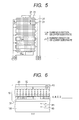
- Fig. 5 is a plan view illustrating an electrode structure according to the present invention to solve the aforementioned problem.
- the electrode structure shown in Fig. 5 is the same as the one described referring to Fig. 22 . That is, the solid line represents the electrode patterns 31 on the lower substrate 30, and the dashed line represents the electrode patterns 21 on the upper substrate 20.
- Fig. 5 is different from Fig. 22 in the rubbing direction on the upper substrate 20, which is at a right angle with the rubbing direction on the lower substrate 30.
- the liquid crystal interposed between the upper substrate 20 and the lower substrate 30 is brought into the twisted structure.
- the angle formed by the rubbing direction P1 on the lower substrate 30 and the rubbing direction P2 on the upper substrate 20 forms a right angle.
- sufficient operation may be obtained so far as the angle is within the range of 90° ⁇ 5°.
- Fig. 6 is a sectional view taken along line Y-Y of Fig. 5 when no voltage is applied between the upper substrate 20 and the lower substrate 30.
- the lower substrate 30 is subjected to rubbing in the direction parallel to the plane of the drawing
- the upper substrate 20 is subjected to rubbing in the direction vertical to the plane of the drawing.
- the incident light to the liquid crystal lens from the liquid crystal display panel emits from the upper substrate while changing the direction of the polarization axis at 90°.
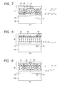
- Fig. 7 is a sectional view taken along line Y-Y of Fig. 5 when the voltage is applied between the upper substrate 20 and the lower substrate 30.
- each rubbing direction on the upper substrate 20 and the lower substrate 30 is the same as the one described referring to Fig. 6 .
- the voltage is applied between the electrode D on the upper substrate 20 and the electrodes A, C on the lower substrate 30.
- the liquid crystal molecules are aligned along the electric force line generated under the voltage to form the convex lens. The aforementioned action is similar to the case described according to Example 1 referring to Figs. 2 and 3 .
- Fig. 8 is a sectional view taken along line X-X of Fig. 5 when no voltage is applied between the upper substrate 20 and the lower substrate 30.
- the rubbing direction on the upper substrate 20 is horizontal with respect to the plane of the drawing, and the rubbing direction on the lower substrate is vertical to the plane of the drawing.
- the light emitted from the liquid crystal display panel 100 is emitted from the upper substrate while changing the direction of the polarization axis at 90°.
- the views shown in Figs. 8 and 6 have an upside-down positional relationship.
- Fig. 9 is a sectional view taken along line X-X of Fig. 5 when the voltage is applied between the upper substrate 20 and the lower substrate 30.
- the rubbing directions on the upper substrate 20 and the lower substrate 30 are similar to the case described referring to Fig. 8 .
- the voltage is applied between the electrodes D, B on the upper substrate 20 and the electrode C on the lower substrate 30.
- the liquid crystal molecules 50 are aligned along the electric force line under the voltage to form the convex lens.
- the convex lens is directed downward.
- the aforementioned action is essentially the same as the action of Example 1 described referring to Figs. 2 and 3 .
- the views shown in Figs. 7 and 9 have the upside-down positional relationship.
- the structure shown in Fig. 9 is capable of stably displaying the 3D images as well.
- the liquid crystal display device capable of selecting the display between vertical and horizontal modes is allowed to stably perform the 3D display.
- the rubbing direction on the upper substrate 20 of the liquid crystal lens 10 is set to be at a right angle with the ground so as to visually recognize the display of the liquid crystal display device even when the polarized sunglasses 400 are used.
Landscapes
- Physics & Mathematics (AREA)
- Nonlinear Science (AREA)
- Engineering & Computer Science (AREA)
- Multimedia (AREA)
- Signal Processing (AREA)
- Mathematical Physics (AREA)
- Chemical & Material Sciences (AREA)
- Crystallography & Structural Chemistry (AREA)
- General Physics & Mathematics (AREA)
- Optics & Photonics (AREA)
- Liquid Crystal (AREA)
- Spectroscopy & Molecular Physics (AREA)
Abstract
Description
- The present invention relates to a display device, and more particularly, to a liquid crystal display device which allows a three-dimensional display using a liquid crystal lens.
- A liquid crystal display panel includes a TFT substrate having pixel electrodes and thin film transistors (TFT) arranged in a matrix, and a counter substrate that is located opposite the TFT substrate, having color filters positioned corresponding to the pixel electrodes on the TFT substrate. A liquid crystal is interposed between the TFT substrate and the counter substrate to form a display region. An image is formed by controlling light transmittance through liquid crystal molecules for each pixel. Since the liquid crystal is capable of controlling only polarization light, a light ray from a backlight is polarized by a lower polarizer before incidence to the TFT substrate, and controlled by a liquid crystal layer. It is further polarized by an upper polarizer again so as to be emitted to the outside. Therefore the light emitted from the liquid crystal display panel becomes polarization light.
- Various methods for forming a three-dimensional image on the liquid crystal display panel have been proposed. Among all of those methods, the one which provides the liquid crystal lens on the liquid crystal display panel has been focused on its application especially to a small-sized display device because of features that no special glasses are required for visual recognition of the three-dimensional image and that selection between the two-dimensional image and the three-dimensional image may be performed.
- Japanese Patent No.
2862462 - Japanese Unexamined Patent Application Publication (Translation of PCT Application) No.
2009-520231 -
Figs. 10 to 13 schematically show aliquid crystal lens 10 and a 3D display using theliquid crystal lens 10. The terms "2D display" and "3D display" herein refer to the "two-dimensional display" and the "three-dimensional display". Theliquid crystal lens 10 has the same structure as the liquid crystal display element, which interposes the liquid crystal between two substrates which form electrodes. However, unlike the liquid crystal display for displaying purpose, it is not intended to be used for the control of polarization direction, and accordingly, no polarizer is used. -
Fig. 10 schematically shows the electrodes formed on the two substrates that interpose the liquid crystal. The electrode on thelower substrate 30 has a transversely long rectangular pattern as indicated by a solid line, and the electrode on theupper substrate 20 has a rectangular pattern as indicated by a dashed line. Rectangular boxes A and B denote electrode terminals that externally apply the voltage. The line which connects the electrode terminal to the electrode on the aforementioned substrate denotes a wiring. The electrode connected to the electrode terminal A may be designated as an electrode A, and the electrode connected to the electrode terminal B may be designated as an electrode B. Basically, each pattern on the upper and lower substrates is not limited, and those patterns may be reversed with respect to the upper and lower substrates. Since transmission of light is required, the transparent electrode such as ITO is used for forming at least the electrode as shown by the dashed line, which entirely covers the display portion. - Arrow P1 shown in
Fig. 10 denotes a rubbing direction on the lower substrate, and arrow P2 denotes a rubbing direction on the upper substrates. The interposed liquid crystal is aligned to have a part at a longer axis side directed toward the arrow direction when no voltage is applied.Fig. 11 is a sectional view taken along line Y-Y ofFig. 10 . The electrodes on thelower substrate 30 are set so that two pixels of a liquidcrystal display panel 100 below theliquid crystal lens 10 are arranged between two electrodes. Actually, a pitch of the two pixels is not the same as the pitch of the electrodes. Those pitches are appropriately designed in accordance with an assumed viewing position. -
Fig. 11 illustrates a state where each voltage applied to the upper and lower electrodes is set to be the same, that is, no voltage is applied to the liquid crystal. In other words, theliquid crystal lens 10 is in an off-state. In this state, the liquid crystal is entirely in an alignment direction regulated through rubbing. Theliquid crystal lens 10 as an optically uniform medium with respect to the transmitted light performs no action, while directly outputting the 2D image on the liquidcrystal display panel 100. -
Fig. 12 illustrates a state where the voltage is applied to the upper and lower electrodes of theliquid crystal lens 10 so as to change the alignment direction of the liquid crystal, that is, theliquid crystal lens 10 is in an on-state. Like the liquidcrystal display panel 100 in a normal state, AC voltage is applied for preventing deterioration in the liquid crystal. The electrode on theupper substrate 20 is flat solid, and the lower electrodes locally exist. Therefore, the electric field applied to the liquid crystal is not uniform in the longitudinal and transverse directions. Along the radial (parabolic) electric field toward the upper solid electrode from the locally positioned lower electrodes, the liquid crystal molecules are also radially aligned as shown in the drawing. - A
liquid crystal molecule 50 exhibits a birefringent property. Polarization light of transmitted light has the component in the longitudinal direction (longer axis direction) of the molecule brought into extraordinary light with high refractive index. The component orthogonal to the one in the longitudinal direction of the molecule is brought into ordinary light with lower refractive index than that of the extraordinary light. The intervening angle may be obtained through resolution into the extraordinary light component and the ordinary light component in the same manner as vector resolution. The birefringent property aligns the liquid crystal as shown inFig. 12 . - If a
polarization direction 40 of the incident light, that is, the light emitted from the liquidcrystal display panel 100 is substantially parallel to the rubbing direction on theliquid crystal lens 10, the ratio between the portion with high refractive index (extraordinary light) and the portion with low refractive index upon passage of the incident light through theliquid crystal lens 10 varies by location. AsFigs. 10 and 11 show, the longer axis direction of theliquid crystal molecule 50 is in line with the rubbing direction which determines an initial alignment of the liquid crystal. - Referring to
Fig. 12 , a dashed line representative of an interface of aconvex lens 11 schematically shows the interface between the portion with high refractive index and the portion with low refractive index. The same effect as the one derived from the convex lens is obtained in the liquid crystal. When two pixels of the liquidcrystal display panel 100 are provided under the effect of the convex lens as shown inFig. 12 , light rays from afirst pixel 200 change the paths mainly to the right side, and light rays from asecond pixel 300 change the paths mainly to the left side. Referring toFig. 12 , each of codes "r", "g" and "b" of thefirst pixel 200 and thesecond pixel 300 denotes a "red sub-pixel", a "green sub-pixel" and a "blue sub-pixel", respectively, common to all the pixels. In the condition where theliquid crystal lens 10 and the liquidcrystal display panel 100 are appropriately designed so that signals for a right eye and a left eye are displayed on thefirst pixel 200 and thesecond pixel 300, the light from thefirst pixel 200 and the light from thesecond pixel 300 may be guided to the right eye and the left eye of a viewer, respectively. This allows the viewer to recognize the 3D image. -
Fig. 13 is a plan view representing a relationship between pixels of the liquidcrystal display panel 100 for right and left eyes andlow electrode patterns 31 of the liquid crystal lens. Referring to the liquidcrystal display panel 100 inFig. 13 , the pixels for the right eye are designated as A1 to A4, and those for the left eye are designated as B1 to B4. -
Fig. 14 illustrates theliquid crystal lens 10 with respect to the pattern configuration of the lowersubstrate electrode patterns 31 and the rubbing direction. Referring toFig. 14 , both the rubbing direction P1 on the upper substrate and the rubbing direction P2 on the lower direction are transverse. Thepolarization direction 40 of emission from the liquid crystal display panel is transverse as well.Fig. 15 is a sectional view of theliquid crystal lens 10 shown inFig. 14 in a state where no voltage is applied between theupper substrate 20 and thelower substrate 30.Fig. 16 is a sectional view of theliquid crystal lens 10 in the state where the voltage is applied between theupper substrate 20 and thelower substrate 30. - A pair of polarized sunglasses as shown in
Fig. 17 may be used when fishing on the seashore, for example, for preventing difficulty in viewing scenery owing to incidence of light reflected from the water surface. The transmission polarization axis of the polarized sunglasses is in a vertical direction as shown inFig. 17 . However, the emission polarization axis of the liquid crystal lens as shown inFigs. 14 to 16 is transverse. When using the polarized sunglasses, the light ray that has passed through the liquid crystal lens may fail to pass through the polarized sunglasses. Accordingly, the viewer cannot see the image on the liquid crystal display device provided with the liquid crystal lens. - The polarization axis of the light ray that has passed through the liquid crystal lens as shown in
Figs. 14 to 16 is in an arrowed direction B shown inFig. 18 . Since the transmission polarization axis of the polarized sunglasses is vertical, the light that has passed through the liquid crystal lens shown inFigs. 14 to 16 cannot be visually recognized through the polarized sunglasses. If the polarization axis of the light which has passed through the liquid crystal lens is in an arrowed direction A, the emitted light is allowed to pass through the polarized sunglasses. -
Figs. 19 to 21 show the liquid crystal lens having the polarization axis of the light emitted from the liquid crystal lens vertically directed.Fig. 19 illustrates the lowersubstrate electrode patterns 31 and the rubbing direction on theliquid crystal lens 10. Referring toFig. 19 , the rubbing direction P1 on the lower substrate and the rubbing direction P2 on the upper direction are vertical. The polarization axis of the light emitted from the liquid crystal display panel is also in the vertical direction. Accordingly, the light that has passed through theliquid crystal lens 10 as shown inFigs. 19 to 21 may be visually recognized through the polarized sunglasses. -
Fig. 20 shows the state where no voltage is applied between theupper substrate 20 and thelower substrate 30 of theliquid crystal lens 10 shown inFig. 19 .Fig. 21 shows the state where the voltage is applied between those substrates. Referring toFig. 20 , since the liquid crystal molecules are not modulated, the light emitted from the liquidcrystal display panel 100 directly passes through theliquid crystal lens 10. Referring toFig. 21 , the voltage is applied between theupper substrate 20 and thelower substrate 30 to form the liquid crystal lens, which enables the 3D display. The polarization axis of the light passing through theliquid crystal lens 10 is in the vertical direction, which may be visually recognized through the polarized sunglasses. - Referring to
Fig. 19 , it is necessary to make a 90° turn of the liquid crystal molecules and align them along the electric field so as to form the convex lens using the liquid crystal molecules. The experimental results of the inventors have clarified the difficulty in forming the liquid crystal lens which enables the clear 3D display. This is mainly considered to be caused by the absence of regulation in the turning direction when making the 90° turn of the liquid crystal molecules. This may generate the region with different alignment such as inverse turn, that is, domain, thus disrupting the interface between the ordinary light and the extraordinary light. - The present invention provides the liquid crystal display device with the liquid crystal lens that enables 3D display, which allows clear visualization of the image from the liquid crystal display device using the polarized sunglasses.
- Meanwhile, on demand from recent application of the liquid crystal display device, the function capable of selectively displaying in the portrait mode (vertical display) and the landscape mode (horizontal display) has been added like the mobile phone. To cope with the desired usage, the 3D panel is required to have the function for selecting the display between the vertical and the horizontal modes.
-
Fig. 22 shows an example of generally employed art which allows theliquid crystal lens 10 to select the display in the vertical and horizontal modes. Like the case as shown inFig. 10 , the solid line indicates the lowersubstrate electrode patterns 31, and the dashed line indicates the uppersubstrate electrode patterns 21. Each of theupper substrate 20 and thelower substrate 30 is formed of narrow electrodes each as the local electrode, and wide electrodes so as to be solid corresponding to the narrow electrodes on the counter substrate. Codes "A", "B", "C" and "D" refer to the terminal electrodes for application of voltage to the respective electrode patterns, and also refer to corresponding electrodes. -
Figs. 23 and24 are sectional views each showing formation of the transversely extending cylindricalliquid crystal lens 10 shown inFig. 22 . The consequence substantially the same as the one described referring toFigs. 11 and12 occurs so as to provide the function of theliquid crystal lens 10. The state shown inFigs. 23 and24 is different from the one shown inFigs. 11 and12 in that a transverse electric field is generated between the electrodes A and C as indicated byFig. 24 . This transverse electric field is substantially in the same direction as the rubbing direction, thus giving no fatal impact on the liquid crystal alignment and the lens effect. -
Figs. 25 and 26 are sectional views each taken along line X-X ofFig. 22 .Fig. 25 shows the state where no voltage is applied to the liquid crystal for 2D display. Theliquid crystal molecules 50 each shown as a circle in the drawing indicates that the longer axis is longitudinally directed with respect to the upper electrode, that is, in the vertical direction with respect to a plane of the drawing.Fig. 26 shows the state where the voltage is applied so that the electric field is generated between the electrode B and the other electrodes A, C and D on theupper substrate 20. LikeFig. 12 orFig. 24 , the liquid crystal is aligned again along the radial electric field directed toward C from B so as to form a downward convex lens shape. The transverse electric field is simultaneously generated between the electrodes B and D on theupper substrate 20. The liquid crystal is also aligned again along this electric field. - In the course of observation that the transverse electric field not only disrupts the configuration of the
liquid crystal lens 10 but also causes the lens effect to disappear, taking a long time (owing to change in the liquid crystal domain) as experimental results, it is found to be difficult to put the above-described selection of the display between the vertical and horizontal modes into practical application. - The present invention provides the liquid crystal display device with the
liquid crystal lens 10 that enables the 3D display, which is capable of selecting the display between the vertical and horizontal modes. - Specifically, the present invention provides a liquid crystal display device having a liquid crystal lens on a liquid crystal display panel.
- (1) The liquid crystal display panel includes a first pixel that contains a red sub-pixel, a green sub-pixel and a blue sub-pixel, and a second pixel that contains a red sub-pixel, a green sub-pixel and a blue sub-pixel. The liquid crystal lens is formed by interposing a liquid crystal between a first substrate and a second substrate. The first substrate has a plurality of electrodes in stripes, which extend in a first direction, and are arranged at predetermined intervals in a second direction. The second substrate has a flat solid electrode. An initial alignment direction of liquid crystal molecules on the first substrate is in line with a polarization axis of light emitted from the liquid crystal display panel as the second direction at a right angle with the first direction. An initial alignment direction of the liquid crystal molecules on the second substrate is set at an angle within a range of 90° ± 5° with respect to the initial alignment direction of the liquid crystal molecules on the first substrate.
- (2) The present invention provides a liquid crystal display device having a liquid crystal lens on a liquid crystal display panel. The liquid crystal display panel includes a first pixel that contains a red sub-pixel, a green sub-pixel and a blue sub-pixel, and a second pixel that contains a red sub-pixel, a green sub-pixel and a blue sub-pixel. The liquid crystal lens is formed by interposing a liquid crystal between a first substrate and a second substrate. The first substrate has a plurality of electrodes in stripes, which extend in a first direction, and are arranged at predetermined intervals in a second direction. The second substrate has a flat solid electrode. An initial alignment direction of liquid crystal molecules on the first substrate is in line with a polarization axis of light emitted from the liquid crystal display panel as the second direction at a right angle with the first direction. An initial alignment direction of the liquid crystal molecules on the second substrate is set at an angle within a range from 45° to 90° with respect to the initial alignment direction of the liquid crystal molecules on the first substrate.
- (3) The present invention provides a liquid crystal display device having a liquid crystal lens on a liquid crystal display panel. The liquid crystal display panel includes pixels that contain red sub-pixels, green sub-pixels, and blue sub-pixels, which are arranged in a first direction at first intervals, and are arranged in a second direction at a right angle with the first direction at second intervals. The liquid crystal lens is formed by interposing a liquid crystal between a first substrate and a second substrate. The first substrate includes a plurality of first narrow electrodes in stripes, extending in the first direction, and arranged in the second direction at intervals each corresponding to a value twice as large as the second interval, and second wide electrodes extend in the first direction at predetermined intervals between the first electrodes. The second substrate includes third narrow electrodes in stripes and fourth wide electrodes in stripes alternately arranged, extending in the second direction, while being arranged in the first direction at predetermined intervals, and the third electrodes are arranged in the first direction at an interval corresponding to a value twice as large as the first interval. An initial alignment direction of the liquid crystal molecules on the first substrate is set at the second direction, and an initial alignment direction of the liquid crystal molecules on the second substrate is set at the first direction. A different voltage is allowed to be applied to each of the first, the second, the third and the fourth electrodes.
- The present invention allows the liquid crystal display device to visualize the 3D image regardless of using the polarized sunglasses, and further allows the selective 3D display between vertical and horizontal modes.
-
-
Fig. 1 is a plan view showing an electrode structure of a liquid crystal lens according to Example 1; -
Fig. 2 is a sectional view taken along line Y-Y ofFig. 1 when no voltage is applied; -
Fig. 3 is a sectional view taken along line Y-Y ofFig. 1 when the voltage is applied; -
Fig. 4 is a plan view showing an electrode structure of a liquid crystal lens according to Example 2; -
Fig. 5 is a plan view showing an electrode structure of a liquid crystal lens according to Example 3; -
Fig. 6 is a sectional view taken along line Y-Y ofFig. 5 when no voltage is applied; -
Fig. 7 is a sectional view taken along line Y-Y ofFig. 5 when the voltage is applied; -
Fig. 8 is a sectional view taken along line X-X ofFig. 5 when no voltage is applied; -
Fig. 9 is a sectional view taken along line X-X ofFig. 5 when the voltage is applied; -
Fig. 10 is a plan view showing an electrode structure of a generally employed liquid crystal lens; -
Fig. 11 is a sectional view taken along line Y-Y ofFig. 10 when no voltage is applied; -
Fig. 12 is a sectional view taken along line Y-Y ofFig. 10 when the voltage is applied; -
Fig. 13 is a plan view schematically representing a relationship between pixels of the liquid crystal display panel and the lower substrate electrode patterns of the liquid crystal lens; -
Fig. 14 is a plan view of the liquid crystal lens when the rubbing direction is set to be horizontal; -
Fig. 15 is a sectional view of the liquid crystal lens shown inFig. 14 when no voltage is applied; -
Fig. 16 is a sectional view of the liquid crystal lens shown inFig. 14 when the voltage is applied; -
Fig. 17 is a view showing a transmission polarization axis of polarized sunglasses; -
Fig. 18 represents an example of the polarization axis of light emission on the liquid crystal display panel; -
Fig. 19 is a plan view of the liquid crystal lens when the rubbing direction is set to be vertical; -
Fig. 20 is a sectional view taken along line X-X ofFig. 19 when no voltage is applied; -
Fig. 21 is a sectional view taken along line X-X ofFig. 19 when the voltage is applied; -
Fig. 22 is a plan view representing an electrode structure of the generally employed liquid crystal lens, capable of selecting the display between vertical mode and horizontal mode; -
Fig. 23 is a sectional view taken along line Y-Y ofFig. 22 when no voltage is applied; -
Fig. 24 is a sectional view taken along line Y-Y ofFig. 22 when the voltage is applied; -
Fig. 25 is a sectional view taken along line X-X ofFig. 22 when no voltage is applied; and -
Fig. 26 is a sectional view taken along line X-X ofFig. 22 when the voltage is applied. - The present invention will be described in detail in reference to the examples. In the following examples, the term "rubbing direction" is used to refer to the direction of the liquid crystal molecules for initial alignment.
- The present invention may be applied to the optical alignment process for the initial alignment of the liquid crystal.
-
Fig. 1 is a plan view illustrating the electrode structure of theliquid crystal lens 10 according to Example 1, and the rubbing directions on theupper substrate 20 and thelower substrate 30. The electrode structure shown inFig. 1 is the same as the electrode structure shown inFig. 10 , and the explanation thereof, thus will be omitted. The structure shown inFig. 1 is different from the one shown inFig. 10 in the rubbing direction on theupper substrate 20. The rubbing direction on thelower substrate 30 is vertical with respect to the extending direction of the lowersubstrate electrode pattern 31 in the same manner as the structure shown inFig. 10 . The rubbing direction on theupper substrate 20 is the same as the extending direction of the lowersubstrate electrode pattern 31. Therefore, the initial alignment of the liquid crystal molecules interposed between theupper substrate 20 and thelower substrate 30 is twisted. -
Fig. 2 is a sectional view of theliquid crystal lens 10 shown inFig. 1 taken along line Y-Y. The structure as illustrated inFig. 2 is the same as the structure shown inFig. 11 except the rubbing direction on theupper substrate 20 and the initial alignment of theliquid crystal molecules 50, and detailed explanations of the structure will be omitted. Referring toFig. 2 , the polarization axis of the light emitted from the liquidcrystal display panel 100 is in the same transverse direction as the rubbing direction on thelower substrate 30 of theliquid crystal lens 10. Meanwhile, the rubbing direction on theupper substrate 20 is at a right angle with the rubbing direction on thelower substrate 30. Then theliquid crystal molecules 50 are aligned parallel to the plane of the drawing around thelower substrate 30, and in the direction vertical to the plane of the drawing around theupper substrate 20. The aforementioned structure is of Twisted Nematic (TN) type.Fig. 2 represents the state of the aforementioned structure where no voltage is applied between theupper substrate 20 and thelower substrate 30. -
Fig. 3 represents the same structure shown inFig. 2 in the state where the voltage is applied between theupper substrate 20 and thelower substrate 30 to form theliquid crystal lens 10 like the convex lens. Theliquid crystal lens 10 extends vertically with respect to the plane of the drawing to form a cylindrical lens. The application of the aforementioned lens for the 3D display allows provision of sufficiently practical images although the resultant brightness is lowered to a certain extent. This is thought to be caused by the residual TN effect, around the center of thelens 10, having the rotary polarization component left to a degree that keeps the viewer nearly imperceptible to the brightness deterioration. - According to the example shown in
Figs. 1 to 3 , the change axis of polarization from theliquid crystal lens 10 may be brought to be in line with the polarization axis ofpolarized sunglasses 400. The image on the liquid crystal display device may be recognized even when thepolarized sunglasses 400 are used. -
Fig. 4 is a plan view of Example 2 according to the present invention, which is the same as Example 1 shown inFig. 1 except the rubbing direction P2 on theupper substrate 20. Referring toFig. 4 , the rubbing direction P2 on theupper substrate 20 is tilted at a predetermined angle θ with respect to the rubbing direction P1 on thelower substrate 30. - The aforementioned structure allows the viewer to visually recognize the 3D image of the
liquid crystal lens 10 using thepolarized sunglasses 400. If the predetermined angle θ is equal to 90° exactly, the viewer is capable of visually recognizing the brightest 3D image. However, the viewer is also capable of visually recognizing the 3D image with the predetermined brightness even when the angle θ is not 90°. That is, application of thepolarized sunglasses 400 may avoid the case where the image is completely invisible like the related art. - In the structure of this example having the angle θ set to 45°, the 2D image on the screen in vertical mode or horizontal mode may be seen accompanied with selection of the display between the vertical and horizontal modes.
- On demand from recent application of the liquid crystal display device, the function capable of selectively displaying in the portrait mode (vertical display) and the landscape mode (horizontal display) has been added, like the mobile phone. To cope with the application, the 3D panel is required to have the function for selecting the display between the vertical and horizontal modes. The generally employed liquid crystal lens structure capable of selectively displaying the 3D images and its problem have been described referring to
Figs. 22 and 23 to 26 as sectional views thereof. - The most notable problem of the related art as shown in
Fig. 26 is that the transverse electric field is generated between the electrodes B and D on the upper substrate, and the liquid crystal is aligned again along the electric field. The transverse electric field not only disrupts the configuration of theliquid crystal lens 10 but also causes the lens effect to disappear over a long time as the liquid crystal domain changes. -
Fig. 5 is a plan view illustrating an electrode structure according to the present invention to solve the aforementioned problem. The electrode structure shown inFig. 5 is the same as the one described referring toFig. 22 . That is, the solid line represents theelectrode patterns 31 on thelower substrate 30, and the dashed line represents theelectrode patterns 21 on theupper substrate 20.Fig. 5 is different fromFig. 22 in the rubbing direction on theupper substrate 20, which is at a right angle with the rubbing direction on thelower substrate 30. The liquid crystal interposed between theupper substrate 20 and thelower substrate 30 is brought into the twisted structure. Optimally, the angle formed by the rubbing direction P1 on thelower substrate 30 and the rubbing direction P2 on theupper substrate 20 forms a right angle. However, sufficient operation may be obtained so far as the angle is within the range of 90° ± 5°. -
Fig. 6 is a sectional view taken along line Y-Y ofFig. 5 when no voltage is applied between theupper substrate 20 and thelower substrate 30. Referring toFig. 6 , thelower substrate 30 is subjected to rubbing in the direction parallel to the plane of the drawing, and theupper substrate 20 is subjected to rubbing in the direction vertical to the plane of the drawing. The incident light to the liquid crystal lens from the liquid crystal display panel emits from the upper substrate while changing the direction of the polarization axis at 90°. -
Fig. 7 is a sectional view taken along line Y-Y ofFig. 5 when the voltage is applied between theupper substrate 20 and thelower substrate 30. Referring toFig. 7 , each rubbing direction on theupper substrate 20 and thelower substrate 30 is the same as the one described referring toFig. 6 . Referring toFig. 7 , the voltage is applied between the electrode D on theupper substrate 20 and the electrodes A, C on thelower substrate 30. The liquid crystal molecules are aligned along the electric force line generated under the voltage to form the convex lens. The aforementioned action is similar to the case described according to Example 1 referring toFigs. 2 and3 . -
Fig. 8 is a sectional view taken along line X-X ofFig. 5 when no voltage is applied between theupper substrate 20 and thelower substrate 30. Referring toFig. 8 , the rubbing direction on theupper substrate 20 is horizontal with respect to the plane of the drawing, and the rubbing direction on the lower substrate is vertical to the plane of the drawing. The light emitted from the liquidcrystal display panel 100 is emitted from the upper substrate while changing the direction of the polarization axis at 90°. The views shown inFigs. 8 and6 have an upside-down positional relationship. -
Fig. 9 is a sectional view taken along line X-X ofFig. 5 when the voltage is applied between theupper substrate 20 and thelower substrate 30. The rubbing directions on theupper substrate 20 and thelower substrate 30 are similar to the case described referring toFig. 8 . Referring toFig. 9 , the voltage is applied between the electrodes D, B on theupper substrate 20 and the electrode C on thelower substrate 30. Theliquid crystal molecules 50 are aligned along the electric force line under the voltage to form the convex lens. The convex lens is directed downward. The aforementioned action is essentially the same as the action of Example 1 described referring toFigs. 2 and3 . The views shown inFigs. 7 and 9 have the upside-down positional relationship. The structure shown inFig. 9 is capable of stably displaying the 3D images as well. - The liquid crystal display device capable of selecting the display between vertical and horizontal modes is allowed to stably perform the 3D display. The rubbing direction on the
upper substrate 20 of theliquid crystal lens 10 is set to be at a right angle with the ground so as to visually recognize the display of the liquid crystal display device even when thepolarized sunglasses 400 are used.
Claims (4)
- A liquid crystal display device having a liquid crystal lens on a liquid crystal display panel,
wherein the liquid crystal display panel includes a first pixel that contains a red sub-pixel, a green sub-pixel and a blue sub-pixel, and a second pixel that contains a red sub-pixel, a green sub-pixel and a blue sub-pixel;
the liquid crystal lens is formed by interposing a liquid crystal between a first substrate and a second substrate;
the first substrate has a plurality of electrodes in stripes, which extend in a first direction, and are arranged at predetermined intervals in a second direction;
the second substrate has a flat solid electrode;
an initial alignment direction of liquid crystal molecules on the first substrate is in line with a polarization axis of light emitted from the liquid crystal display panel as the second direction at a right angle with the first direction; and
an initial alignment direction of the liquid crystal molecules on the second substrate is set at an angle within a range of 90° ± 5° with respect to the initial alignment direction of the liquid crystal molecules on the first substrate. - The liquid crystal display device according to claim 1, wherein an angle of 90° is formed between the initial alignment direction of the liquid crystal molecules on the second substrate and the initial alignment direction of the liquid crystal molecules on the first substrate.
- A liquid crystal display device having a liquid crystal lens on a liquid crystal display panel,
wherein the liquid crystal display panel includes a first pixel that contains a red sub-pixel, a green sub-pixel and a blue sub-pixel, and a second pixel that contains a red sub-pixel, a green sub-pixel and a blue sub-pixel;
the liquid crystal lens is formed by interposing a liquid crystal between a first substrate and a second substrate;
the first substrate has a plurality of electrodes in stripes, which extend in a first direction, and are arranged at predetermined intervals in a second direction;
the second substrate has a flat solid electrode;
an initial alignment direction of liquid crystal molecules on the first substrate is in line with a polarization axis of light emitted from the liquid crystal display panel as the second direction at a right angle with the first direction; and
an initial alignment direction of the liquid crystal molecules on the second substrate is set at an angle within a range from 45° to 90° with respect to the initial alignment direction of the liquid crystal molecules on the first substrate. - A liquid crystal display device having a liquid crystal lens on a liquid crystal display panel,
wherein the liquid crystal display panel includes pixels that contain red sub-pixels, green sub-pixels, and blue sub-pixels, which are arranged in a first direction at first intervals, and are arranged in a second direction at a right angle with the first direction at second intervals;
the liquid crystal lens is formed by interposing a liquid crystal between a first substrate and a second substrate;
the first substrate includes a plurality of first narrow electrodes in stripes, extending in the first direction, and arranged in the second direction at intervals each corresponding to a value twice as large as the second interval, and second wide electrodes extend in the first direction at predetermined intervals between the first electrodes;
the second substrate includes third narrow electrodes in stripes and fourth wide electrodes in stripes alternately arranged, extending in the second direction, while being arranged in the first direction at predetermined intervals, and the third electrodes are arranged in the first direction at an interval corresponding to a value twice as large as the first interval;
an initial alignment direction of the liquid crystal molecules on the first substrate is set at the second direction, and an initial alignment direction of the liquid crystal molecules on the second substrate is set at the first direction; and
a different voltage is allowed to be applied to each of the first, the second, the third and the fourth electrodes.
Applications Claiming Priority (1)
| Application Number | Priority Date | Filing Date | Title |
|---|---|---|---|
| JP2011086293A JP5301605B2 (en) | 2011-04-08 | 2011-04-08 | Liquid crystal display |
Publications (2)
| Publication Number | Publication Date |
|---|---|
| EP2509331A1 true EP2509331A1 (en) | 2012-10-10 |
| EP2509331B1 EP2509331B1 (en) | 2017-01-04 |
Family
ID=46045742
Family Applications (1)
| Application Number | Title | Priority Date | Filing Date |
|---|---|---|---|
| EP12163434.9A Active EP2509331B1 (en) | 2011-04-08 | 2012-04-05 | Liquid crystal display device |
Country Status (6)
| Country | Link |
|---|---|
| US (1) | US9709863B2 (en) |
| EP (1) | EP2509331B1 (en) |
| JP (1) | JP5301605B2 (en) |
| KR (1) | KR101357347B1 (en) |
| CN (1) | CN102736330B (en) |
| TW (1) | TWI474080B (en) |
Cited By (1)
| Publication number | Priority date | Publication date | Assignee | Title |
|---|---|---|---|---|
| TWI479199B (en) * | 2013-01-21 | 2015-04-01 | Au Optronics Corp | 2d and 3d switchable display device and liquid crystal lenticular lens thereof |
Families Citing this family (20)
| Publication number | Priority date | Publication date | Assignee | Title |
|---|---|---|---|---|
| JP2014081419A (en) * | 2012-10-15 | 2014-05-08 | Japan Display Inc | Liquid crystal display device |
| JP2014081433A (en) * | 2012-10-15 | 2014-05-08 | Japan Display Inc | Three-dimensional image display device |
| JP5980097B2 (en) * | 2012-11-07 | 2016-08-31 | 株式会社ジャパンディスプレイ | Image display device and liquid crystal lens |
| CN103969911B (en) * | 2013-02-28 | 2017-01-18 | 上海天马微电子有限公司 | Electronic control liquid crystal lens panel and 3D/2D switchable stereoscopic display device |
| CN103293689B (en) * | 2013-05-31 | 2015-05-13 | 京东方科技集团股份有限公司 | Method capable of switching between different display modes and display device |
| JPWO2014196125A1 (en) * | 2013-06-05 | 2017-02-23 | パナソニックIpマネジメント株式会社 | Image display device and liquid crystal lens |
| KR102232621B1 (en) * | 2013-07-30 | 2021-03-29 | 삼성디스플레이 주식회사 | Display apparatus providing light therapy |
| JP2015084079A (en) | 2013-09-20 | 2015-04-30 | パナソニックIpマネジメント株式会社 | Image display device |
| KR102061234B1 (en) | 2013-10-28 | 2020-01-02 | 삼성디스플레이 주식회사 | Display device and liquid crystal lends panel for the same |
| JP6200789B2 (en) * | 2013-11-27 | 2017-09-20 | 株式会社ジャパンディスプレイ | Display device |
| KR20150061967A (en) | 2013-11-28 | 2015-06-05 | 삼성디스플레이 주식회사 | Display device |
| KR20150081102A (en) | 2014-01-03 | 2015-07-13 | 삼성디스플레이 주식회사 | Liquid crystal lens and panel and display device including liquid crystal lens panel |
| KR20150086762A (en) | 2014-01-20 | 2015-07-29 | 삼성디스플레이 주식회사 | Display device |
| CN103984181B (en) * | 2014-03-12 | 2017-02-15 | 京东方科技集团股份有限公司 | Liquid crystal lens and display device |
| KR102221553B1 (en) | 2014-05-09 | 2021-03-02 | 삼성디스플레이 주식회사 | Display device and liquid crystal lends panel device for the same |
| KR102207192B1 (en) * | 2014-09-30 | 2021-01-25 | 엘지디스플레이 주식회사 | Polarizing Control Film and Stereoscopic Display Device Using the Same |
| US9904502B2 (en) | 2015-08-05 | 2018-02-27 | Apple Inc. | Dual display equipment with enhanced visibility and suppressed reflections |
| CN106855675B (en) * | 2017-03-14 | 2020-01-07 | 京东方科技集团股份有限公司 | Anti-peep devices and anti-peep display devices |
| DE112019002704A5 (en) * | 2018-05-29 | 2021-07-15 | Seereal Technologies S.A. | DIFFACTIVE OPTICAL ELEMENT AND DISPLAY DEVICE |
| TWI750093B (en) * | 2021-05-14 | 2021-12-11 | 友達光電股份有限公司 | Display apparatus |
Citations (4)
| Publication number | Priority date | Publication date | Assignee | Title |
|---|---|---|---|---|
| JP2862462B2 (en) | 1993-09-09 | 1999-03-03 | シャープ株式会社 | 3D display device |
| WO2004070467A2 (en) * | 2003-02-05 | 2004-08-19 | Ocuity Limited | Switchable birefringent cylindrical lens array |
| JP2009520231A (en) | 2005-12-20 | 2009-05-21 | コーニンクレッカ フィリップス エレクトロニクス エヌ ヴィ | Autostereoscopic display device |
| US20100157181A1 (en) * | 2008-12-22 | 2010-06-24 | Sony Corporation | Lens array device and image display |
Family Cites Families (13)
| Publication number | Priority date | Publication date | Assignee | Title |
|---|---|---|---|---|
| US5493427A (en) | 1993-05-25 | 1996-02-20 | Sharp Kabushiki Kaisha | Three-dimensional display unit with a variable lens |
| GB2411735A (en) * | 2004-03-06 | 2005-09-07 | Sharp Kk | Control of liquid crystal alignment in an optical device |
| KR101201848B1 (en) * | 2006-02-20 | 2012-11-15 | 삼성디스플레이 주식회사 | Stereo-scopic image conversion panel and stereo-scopic image display apparatus having the same |
| KR20080003072A (en) * | 2006-06-30 | 2008-01-07 | 엘지.필립스 엘시디 주식회사 | Narrow-view angle display device and wide / narrow-view angle switchable display device |
| GB2443649A (en) | 2006-11-07 | 2008-05-14 | Sharp Kk | Liquid crystal device having splay-twist and splay-bend mode |
| US20100149444A1 (en) * | 2007-04-17 | 2010-06-17 | Koninklijke Philips Electronics N.V. | Beam-shaping device |
| RU2377623C2 (en) * | 2007-04-20 | 2009-12-27 | Василий Александрович ЕЖОВ | Method of viewing stereo images with complete resolution for each aspect and device to this end |
| CN101387758A (en) * | 2007-09-14 | 2009-03-18 | 北京超多维科技有限公司 | 2D-3D convertible stereo display device |
| KR101222990B1 (en) * | 2007-10-22 | 2013-01-18 | 엘지디스플레이 주식회사 | Liquid Crystal Lens Electrically driven and Stereoscopy Display Device |
| JP5667752B2 (en) * | 2009-08-20 | 2015-02-12 | 株式会社ジャパンディスプレイ | 3D image display device |
| KR101993566B1 (en) * | 2009-12-01 | 2019-06-26 | 시리얼 테크놀로지즈 에스.에이. | Phase modulator for modulating light interacting with the phase modulator |
| KR20110078788A (en) * | 2009-12-31 | 2011-07-07 | 엘지디스플레이 주식회사 | Liquid Crystal Field Lens and Stereoscopic Display Device Using the Same |
| TWM396974U (en) * | 2010-05-21 | 2011-01-21 | Chunghwa Picture Tubes Ltd | Displaying apparatus for switching displaying modes |
-
2011
- 2011-04-08 JP JP2011086293A patent/JP5301605B2/en active Active
-
2012
- 2012-03-14 TW TW101108721A patent/TWI474080B/en active
- 2012-04-03 US US13/437,982 patent/US9709863B2/en active Active
- 2012-04-05 EP EP12163434.9A patent/EP2509331B1/en active Active
- 2012-04-06 KR KR1020120036067A patent/KR101357347B1/en active Active
- 2012-04-06 CN CN201210104943.XA patent/CN102736330B/en active Active
Patent Citations (4)
| Publication number | Priority date | Publication date | Assignee | Title |
|---|---|---|---|---|
| JP2862462B2 (en) | 1993-09-09 | 1999-03-03 | シャープ株式会社 | 3D display device |
| WO2004070467A2 (en) * | 2003-02-05 | 2004-08-19 | Ocuity Limited | Switchable birefringent cylindrical lens array |
| JP2009520231A (en) | 2005-12-20 | 2009-05-21 | コーニンクレッカ フィリップス エレクトロニクス エヌ ヴィ | Autostereoscopic display device |
| US20100157181A1 (en) * | 2008-12-22 | 2010-06-24 | Sony Corporation | Lens array device and image display |
Cited By (1)
| Publication number | Priority date | Publication date | Assignee | Title |
|---|---|---|---|---|
| TWI479199B (en) * | 2013-01-21 | 2015-04-01 | Au Optronics Corp | 2d and 3d switchable display device and liquid crystal lenticular lens thereof |
Also Published As
| Publication number | Publication date |
|---|---|
| KR101357347B1 (en) | 2014-02-03 |
| TWI474080B (en) | 2015-02-21 |
| US20120257127A1 (en) | 2012-10-11 |
| JP2012220719A (en) | 2012-11-12 |
| CN102736330B (en) | 2015-03-18 |
| JP5301605B2 (en) | 2013-09-25 |
| CN102736330A (en) | 2012-10-17 |
| TW201248257A (en) | 2012-12-01 |
| US9709863B2 (en) | 2017-07-18 |
| KR20120115149A (en) | 2012-10-17 |
| EP2509331B1 (en) | 2017-01-04 |
Similar Documents
| Publication | Publication Date | Title |
|---|---|---|
| EP2509331B1 (en) | Liquid crystal display device | |
| US9110359B2 (en) | Display device | |
| US8345088B2 (en) | Autostereoscopic display apparatus | |
| US20130293793A1 (en) | Display apparatus and control method thereof | |
| US8587737B2 (en) | Display device | |
| US9405138B2 (en) | Liquid crystal display device | |
| KR20120018280A (en) | Light barrier device and display unit | |
| EP2629135B1 (en) | Display device | |
| WO2012096032A1 (en) | Three-dimensional image display device | |
| WO2014063486A1 (en) | Two-dimensional and three-dimensional switchable liquid crystal display device and displaying method thereof | |
| KR102144733B1 (en) | Stereopsis image display device | |
| CN102749762A (en) | Display device | |
| JP2005172848A (en) | Display panel and display device | |
| US9417455B2 (en) | Image display device | |
| JP6207355B2 (en) | 3D display device | |
| JP5710696B2 (en) | Display device | |
| JP2015018282A (en) | Liquid crystal display | |
| CN103733125A (en) | Stereoscopic display device | |
| CN103217802A (en) | Liquid crystal display panel and device thereof | |
| KR20120120017A (en) | Display device | |
| KR20190027539A (en) | Switchable Type Display Device And Method Of Driving The Same |
Legal Events
| Date | Code | Title | Description |
|---|---|---|---|
| PUAI | Public reference made under article 153(3) epc to a published international application that has entered the european phase |
Free format text: ORIGINAL CODE: 0009012 |
|
| AK | Designated contracting states |
Kind code of ref document: A1 Designated state(s): AL AT BE BG CH CY CZ DE DK EE ES FI FR GB GR HR HU IE IS IT LI LT LU LV MC MK MT NL NO PL PT RO RS SE SI SK SM TR |
|
| AX | Request for extension of the european patent |
Extension state: BA ME |
|
| RIN1 | Information on inventor provided before grant (corrected) |
Inventor name: MIYAZAWA, TOSHIO Inventor name: SUGITA, TATSUYA Inventor name: OKA, SHINICHIRO Inventor name: SAITOU, TERUNORI |
|
| 17P | Request for examination filed |
Effective date: 20130410 |
|
| 17Q | First examination report despatched |
Effective date: 20150204 |
|
| GRAP | Despatch of communication of intention to grant a patent |
Free format text: ORIGINAL CODE: EPIDOSNIGR1 |
|
| INTG | Intention to grant announced |
Effective date: 20160922 |
|
| STAA | Information on the status of an ep patent application or granted ep patent |
Free format text: STATUS: GRANT OF PATENT IS INTENDED |
|
| GRAS | Grant fee paid |
Free format text: ORIGINAL CODE: EPIDOSNIGR3 |
|
| GRAA | (expected) grant |
Free format text: ORIGINAL CODE: 0009210 |
|
| STAA | Information on the status of an ep patent application or granted ep patent |
Free format text: STATUS: THE PATENT HAS BEEN GRANTED |
|
| AK | Designated contracting states |
Kind code of ref document: B1 Designated state(s): AL AT BE BG CH CY CZ DE DK EE ES FI FR GB GR HR HU IE IS IT LI LT LU LV MC MK MT NL NO PL PT RO RS SE SI SK SM TR |
|
| RAP1 | Party data changed (applicant data changed or rights of an application transferred) |
Owner name: JAPAN DISPLAY INC. |
|
| REG | Reference to a national code |
Ref country code: GB Ref legal event code: FG4D |
|
| REG | Reference to a national code |
Ref country code: CH Ref legal event code: EP |
|
| REG | Reference to a national code |
Ref country code: AT Ref legal event code: REF Ref document number: 860271 Country of ref document: AT Kind code of ref document: T Effective date: 20170115 |
|
| REG | Reference to a national code |
Ref country code: IE Ref legal event code: FG4D |
|
| REG | Reference to a national code |
Ref country code: DE Ref legal event code: R096 Ref document number: 602012027289 Country of ref document: DE |
|
| REG | Reference to a national code |
Ref country code: LT Ref legal event code: MG4D Ref country code: NL Ref legal event code: MP Effective date: 20170104 |
|
| REG | Reference to a national code |
Ref country code: AT Ref legal event code: MK05 Ref document number: 860271 Country of ref document: AT Kind code of ref document: T Effective date: 20170104 |
|
| PG25 | Lapsed in a contracting state [announced via postgrant information from national office to epo] |
Ref country code: NL Free format text: LAPSE BECAUSE OF FAILURE TO SUBMIT A TRANSLATION OF THE DESCRIPTION OR TO PAY THE FEE WITHIN THE PRESCRIBED TIME-LIMIT Effective date: 20170104 |
|
| PG25 | Lapsed in a contracting state [announced via postgrant information from national office to epo] |
Ref country code: GR Free format text: LAPSE BECAUSE OF FAILURE TO SUBMIT A TRANSLATION OF THE DESCRIPTION OR TO PAY THE FEE WITHIN THE PRESCRIBED TIME-LIMIT Effective date: 20170405 Ref country code: HR Free format text: LAPSE BECAUSE OF FAILURE TO SUBMIT A TRANSLATION OF THE DESCRIPTION OR TO PAY THE FEE WITHIN THE PRESCRIBED TIME-LIMIT Effective date: 20170104 Ref country code: NO Free format text: LAPSE BECAUSE OF FAILURE TO SUBMIT A TRANSLATION OF THE DESCRIPTION OR TO PAY THE FEE WITHIN THE PRESCRIBED TIME-LIMIT Effective date: 20170404 Ref country code: FI Free format text: LAPSE BECAUSE OF FAILURE TO SUBMIT A TRANSLATION OF THE DESCRIPTION OR TO PAY THE FEE WITHIN THE PRESCRIBED TIME-LIMIT Effective date: 20170104 Ref country code: LT Free format text: LAPSE BECAUSE OF FAILURE TO SUBMIT A TRANSLATION OF THE DESCRIPTION OR TO PAY THE FEE WITHIN THE PRESCRIBED TIME-LIMIT Effective date: 20170104 Ref country code: IS Free format text: LAPSE BECAUSE OF FAILURE TO SUBMIT A TRANSLATION OF THE DESCRIPTION OR TO PAY THE FEE WITHIN THE PRESCRIBED TIME-LIMIT Effective date: 20170504 |
|
| PG25 | Lapsed in a contracting state [announced via postgrant information from national office to epo] |
Ref country code: AT Free format text: LAPSE BECAUSE OF FAILURE TO SUBMIT A TRANSLATION OF THE DESCRIPTION OR TO PAY THE FEE WITHIN THE PRESCRIBED TIME-LIMIT Effective date: 20170104 Ref country code: ES Free format text: LAPSE BECAUSE OF FAILURE TO SUBMIT A TRANSLATION OF THE DESCRIPTION OR TO PAY THE FEE WITHIN THE PRESCRIBED TIME-LIMIT Effective date: 20170104 Ref country code: RS Free format text: LAPSE BECAUSE OF FAILURE TO SUBMIT A TRANSLATION OF THE DESCRIPTION OR TO PAY THE FEE WITHIN THE PRESCRIBED TIME-LIMIT Effective date: 20170104 Ref country code: BG Free format text: LAPSE BECAUSE OF FAILURE TO SUBMIT A TRANSLATION OF THE DESCRIPTION OR TO PAY THE FEE WITHIN THE PRESCRIBED TIME-LIMIT Effective date: 20170404 Ref country code: PT Free format text: LAPSE BECAUSE OF FAILURE TO SUBMIT A TRANSLATION OF THE DESCRIPTION OR TO PAY THE FEE WITHIN THE PRESCRIBED TIME-LIMIT Effective date: 20170504 Ref country code: LV Free format text: LAPSE BECAUSE OF FAILURE TO SUBMIT A TRANSLATION OF THE DESCRIPTION OR TO PAY THE FEE WITHIN THE PRESCRIBED TIME-LIMIT Effective date: 20170104 Ref country code: PL Free format text: LAPSE BECAUSE OF FAILURE TO SUBMIT A TRANSLATION OF THE DESCRIPTION OR TO PAY THE FEE WITHIN THE PRESCRIBED TIME-LIMIT Effective date: 20170104 Ref country code: SE Free format text: LAPSE BECAUSE OF FAILURE TO SUBMIT A TRANSLATION OF THE DESCRIPTION OR TO PAY THE FEE WITHIN THE PRESCRIBED TIME-LIMIT Effective date: 20170104 |
|
| REG | Reference to a national code |
Ref country code: DE Ref legal event code: R097 Ref document number: 602012027289 Country of ref document: DE |
|
| PG25 | Lapsed in a contracting state [announced via postgrant information from national office to epo] |
Ref country code: CZ Free format text: LAPSE BECAUSE OF FAILURE TO SUBMIT A TRANSLATION OF THE DESCRIPTION OR TO PAY THE FEE WITHIN THE PRESCRIBED TIME-LIMIT Effective date: 20170104 Ref country code: IT Free format text: LAPSE BECAUSE OF FAILURE TO SUBMIT A TRANSLATION OF THE DESCRIPTION OR TO PAY THE FEE WITHIN THE PRESCRIBED TIME-LIMIT Effective date: 20170104 Ref country code: RO Free format text: LAPSE BECAUSE OF FAILURE TO SUBMIT A TRANSLATION OF THE DESCRIPTION OR TO PAY THE FEE WITHIN THE PRESCRIBED TIME-LIMIT Effective date: 20170104 Ref country code: SK Free format text: LAPSE BECAUSE OF FAILURE TO SUBMIT A TRANSLATION OF THE DESCRIPTION OR TO PAY THE FEE WITHIN THE PRESCRIBED TIME-LIMIT Effective date: 20170104 Ref country code: EE Free format text: LAPSE BECAUSE OF FAILURE TO SUBMIT A TRANSLATION OF THE DESCRIPTION OR TO PAY THE FEE WITHIN THE PRESCRIBED TIME-LIMIT Effective date: 20170104 |
|
| PLBE | No opposition filed within time limit |
Free format text: ORIGINAL CODE: 0009261 |
|
| STAA | Information on the status of an ep patent application or granted ep patent |
Free format text: STATUS: NO OPPOSITION FILED WITHIN TIME LIMIT |
|
| REG | Reference to a national code |
Ref country code: DE Ref legal event code: R079 Ref document number: 602012027289 Country of ref document: DE Free format text: PREVIOUS MAIN CLASS: H04N0013040000 Ipc: H04N0013300000 |
|
| PG25 | Lapsed in a contracting state [announced via postgrant information from national office to epo] |
Ref country code: SM Free format text: LAPSE BECAUSE OF FAILURE TO SUBMIT A TRANSLATION OF THE DESCRIPTION OR TO PAY THE FEE WITHIN THE PRESCRIBED TIME-LIMIT Effective date: 20170104 Ref country code: DK Free format text: LAPSE BECAUSE OF FAILURE TO SUBMIT A TRANSLATION OF THE DESCRIPTION OR TO PAY THE FEE WITHIN THE PRESCRIBED TIME-LIMIT Effective date: 20170104 |
|
| REG | Reference to a national code |
Ref country code: CH Ref legal event code: PL |
|
| 26N | No opposition filed |
Effective date: 20171005 |
|
| REG | Reference to a national code |
Ref country code: IE Ref legal event code: MM4A |
|
| REG | Reference to a national code |
Ref country code: FR Ref legal event code: ST Effective date: 20171229 |
|
| PG25 | Lapsed in a contracting state [announced via postgrant information from national office to epo] |
Ref country code: MC Free format text: LAPSE BECAUSE OF FAILURE TO SUBMIT A TRANSLATION OF THE DESCRIPTION OR TO PAY THE FEE WITHIN THE PRESCRIBED TIME-LIMIT Effective date: 20170104 Ref country code: FR Free format text: LAPSE BECAUSE OF NON-PAYMENT OF DUE FEES Effective date: 20170502 |
|
| PG25 | Lapsed in a contracting state [announced via postgrant information from national office to epo] |
Ref country code: LU Free format text: LAPSE BECAUSE OF NON-PAYMENT OF DUE FEES Effective date: 20170405 Ref country code: LI Free format text: LAPSE BECAUSE OF NON-PAYMENT OF DUE FEES Effective date: 20170430 Ref country code: CH Free format text: LAPSE BECAUSE OF NON-PAYMENT OF DUE FEES Effective date: 20170430 Ref country code: SI Free format text: LAPSE BECAUSE OF FAILURE TO SUBMIT A TRANSLATION OF THE DESCRIPTION OR TO PAY THE FEE WITHIN THE PRESCRIBED TIME-LIMIT Effective date: 20170104 |
|
| REG | Reference to a national code |
Ref country code: BE Ref legal event code: MM Effective date: 20170430 |
|
| PG25 | Lapsed in a contracting state [announced via postgrant information from national office to epo] |
Ref country code: IE Free format text: LAPSE BECAUSE OF NON-PAYMENT OF DUE FEES Effective date: 20170405 |
|
| PG25 | Lapsed in a contracting state [announced via postgrant information from national office to epo] |
Ref country code: BE Free format text: LAPSE BECAUSE OF NON-PAYMENT OF DUE FEES Effective date: 20170430 |
|
| PG25 | Lapsed in a contracting state [announced via postgrant information from national office to epo] |
Ref country code: MT Free format text: LAPSE BECAUSE OF NON-PAYMENT OF DUE FEES Effective date: 20170405 |
|
| PG25 | Lapsed in a contracting state [announced via postgrant information from national office to epo] |
Ref country code: HU Free format text: LAPSE BECAUSE OF FAILURE TO SUBMIT A TRANSLATION OF THE DESCRIPTION OR TO PAY THE FEE WITHIN THE PRESCRIBED TIME-LIMIT; INVALID AB INITIO Effective date: 20120405 |
|
| PG25 | Lapsed in a contracting state [announced via postgrant information from national office to epo] |
Ref country code: CY Free format text: LAPSE BECAUSE OF NON-PAYMENT OF DUE FEES Effective date: 20170104 |
|
| PG25 | Lapsed in a contracting state [announced via postgrant information from national office to epo] |
Ref country code: MK Free format text: LAPSE BECAUSE OF FAILURE TO SUBMIT A TRANSLATION OF THE DESCRIPTION OR TO PAY THE FEE WITHIN THE PRESCRIBED TIME-LIMIT Effective date: 20170104 |
|
| PG25 | Lapsed in a contracting state [announced via postgrant information from national office to epo] |
Ref country code: TR Free format text: LAPSE BECAUSE OF FAILURE TO SUBMIT A TRANSLATION OF THE DESCRIPTION OR TO PAY THE FEE WITHIN THE PRESCRIBED TIME-LIMIT Effective date: 20170104 |
|
| PG25 | Lapsed in a contracting state [announced via postgrant information from national office to epo] |
Ref country code: AL Free format text: LAPSE BECAUSE OF FAILURE TO SUBMIT A TRANSLATION OF THE DESCRIPTION OR TO PAY THE FEE WITHIN THE PRESCRIBED TIME-LIMIT Effective date: 20170104 |
|
| PGFP | Annual fee paid to national office [announced via postgrant information from national office to epo] |
Ref country code: DE Payment date: 20250422 Year of fee payment: 14 |
|
| PGFP | Annual fee paid to national office [announced via postgrant information from national office to epo] |
Ref country code: GB Payment date: 20250423 Year of fee payment: 14 |
|
| REG | Reference to a national code |
Ref country code: GB Ref legal event code: 732E Free format text: REGISTERED BETWEEN 20250724 AND 20250730 |
|
| REG | Reference to a national code |
Ref country code: DE Ref legal event code: R081 Ref document number: 602012027289 Country of ref document: DE Owner name: MAGNOLIA WHITE CORPORATION, JP Free format text: FORMER OWNER: JAPAN DISPLAY INC., TOKYO, JP Ref country code: DE Ref legal event code: R082 Ref document number: 602012027289 Country of ref document: DE Representative=s name: MERH-IP MATIAS ERNY REICHL HOFFMANN PATENTANWA, DE |