JP6207355B2 - 3D display device - Google Patents
3D display device Download PDFInfo
- Publication number
- JP6207355B2 JP6207355B2 JP2013238131A JP2013238131A JP6207355B2 JP 6207355 B2 JP6207355 B2 JP 6207355B2 JP 2013238131 A JP2013238131 A JP 2013238131A JP 2013238131 A JP2013238131 A JP 2013238131A JP 6207355 B2 JP6207355 B2 JP 6207355B2
- Authority
- JP
- Japan
- Prior art keywords
- barrier
- substrate
- electrode
- liquid crystal
- panel
- Prior art date
- Legal status (The legal status is an assumption and is not a legal conclusion. Google has not performed a legal analysis and makes no representation as to the accuracy of the status listed.)
- Active
Links
- 230000004888 barrier function Effects 0.000 claims description 294
- 239000000758 substrate Substances 0.000 claims description 148
- 239000004973 liquid crystal related substance Substances 0.000 claims description 94
- 230000004044 response Effects 0.000 claims description 6
- 230000005540 biological transmission Effects 0.000 description 47
- 238000000034 method Methods 0.000 description 18
- 238000010586 diagram Methods 0.000 description 15
- 238000002834 transmittance Methods 0.000 description 13
- 244000126211 Hericium coralloides Species 0.000 description 10
- 230000000694 effects Effects 0.000 description 7
- 230000000052 comparative effect Effects 0.000 description 5
- 239000010410 layer Substances 0.000 description 5
- 230000010287 polarization Effects 0.000 description 5
- 230000005684 electric field Effects 0.000 description 4
- 230000015572 biosynthetic process Effects 0.000 description 3
- 230000008859 change Effects 0.000 description 3
- 239000000853 adhesive Substances 0.000 description 2
- 230000001070 adhesive effect Effects 0.000 description 2
- 238000005452 bending Methods 0.000 description 2
- 230000007423 decrease Effects 0.000 description 2
- 230000006866 deterioration Effects 0.000 description 2
- 239000011521 glass Substances 0.000 description 2
- 230000003287 optical effect Effects 0.000 description 2
- 230000008901 benefit Effects 0.000 description 1
- 230000015556 catabolic process Effects 0.000 description 1
- 238000006731 degradation reaction Methods 0.000 description 1
- 230000000593 degrading effect Effects 0.000 description 1
- 238000009792 diffusion process Methods 0.000 description 1
- 230000004313 glare Effects 0.000 description 1
- 239000011229 interlayer Substances 0.000 description 1
- 230000035699 permeability Effects 0.000 description 1
- 230000009467 reduction Effects 0.000 description 1
Images


Classifications
-
- G—PHYSICS
- G02—OPTICS
- G02B—OPTICAL ELEMENTS, SYSTEMS OR APPARATUS
- G02B27/00—Optical systems or apparatus not provided for by any of the groups G02B1/00 - G02B26/00, G02B30/00
- G02B27/0093—Optical systems or apparatus not provided for by any of the groups G02B1/00 - G02B26/00, G02B30/00 with means for monitoring data relating to the user, e.g. head-tracking, eye-tracking
-
- G—PHYSICS
- G02—OPTICS
- G02B—OPTICAL ELEMENTS, SYSTEMS OR APPARATUS
- G02B30/00—Optical systems or apparatus for producing three-dimensional [3D] effects, e.g. stereoscopic images
- G02B30/20—Optical systems or apparatus for producing three-dimensional [3D] effects, e.g. stereoscopic images by providing first and second parallax images to an observer's left and right eyes
- G02B30/26—Optical systems or apparatus for producing three-dimensional [3D] effects, e.g. stereoscopic images by providing first and second parallax images to an observer's left and right eyes of the autostereoscopic type
- G02B30/27—Optical systems or apparatus for producing three-dimensional [3D] effects, e.g. stereoscopic images by providing first and second parallax images to an observer's left and right eyes of the autostereoscopic type involving lenticular arrays
-
- G—PHYSICS
- G02—OPTICS
- G02B—OPTICAL ELEMENTS, SYSTEMS OR APPARATUS
- G02B30/00—Optical systems or apparatus for producing three-dimensional [3D] effects, e.g. stereoscopic images
- G02B30/20—Optical systems or apparatus for producing three-dimensional [3D] effects, e.g. stereoscopic images by providing first and second parallax images to an observer's left and right eyes
- G02B30/26—Optical systems or apparatus for producing three-dimensional [3D] effects, e.g. stereoscopic images by providing first and second parallax images to an observer's left and right eyes of the autostereoscopic type
- G02B30/30—Optical systems or apparatus for producing three-dimensional [3D] effects, e.g. stereoscopic images by providing first and second parallax images to an observer's left and right eyes of the autostereoscopic type involving parallax barriers
- G02B30/31—Optical systems or apparatus for producing three-dimensional [3D] effects, e.g. stereoscopic images by providing first and second parallax images to an observer's left and right eyes of the autostereoscopic type involving parallax barriers involving active parallax barriers
-
- G—PHYSICS
- G02—OPTICS
- G02F—OPTICAL DEVICES OR ARRANGEMENTS FOR THE CONTROL OF LIGHT BY MODIFICATION OF THE OPTICAL PROPERTIES OF THE MEDIA OF THE ELEMENTS INVOLVED THEREIN; NON-LINEAR OPTICS; FREQUENCY-CHANGING OF LIGHT; OPTICAL LOGIC ELEMENTS; OPTICAL ANALOGUE/DIGITAL CONVERTERS
- G02F1/00—Devices or arrangements for the control of the intensity, colour, phase, polarisation or direction of light arriving from an independent light source, e.g. switching, gating or modulating; Non-linear optics
- G02F1/01—Devices or arrangements for the control of the intensity, colour, phase, polarisation or direction of light arriving from an independent light source, e.g. switching, gating or modulating; Non-linear optics for the control of the intensity, phase, polarisation or colour
- G02F1/13—Devices or arrangements for the control of the intensity, colour, phase, polarisation or direction of light arriving from an independent light source, e.g. switching, gating or modulating; Non-linear optics for the control of the intensity, phase, polarisation or colour based on liquid crystals, e.g. single liquid crystal display cells
- G02F1/133—Constructional arrangements; Operation of liquid crystal cells; Circuit arrangements
- G02F1/1333—Constructional arrangements; Manufacturing methods
- G02F1/1343—Electrodes
- G02F1/134309—Electrodes characterised by their geometrical arrangement
- G02F1/134363—Electrodes characterised by their geometrical arrangement for applying an electric field parallel to the substrate, i.e. in-plane switching [IPS]
-
- H—ELECTRICITY
- H04—ELECTRIC COMMUNICATION TECHNIQUE
- H04N—PICTORIAL COMMUNICATION, e.g. TELEVISION
- H04N13/00—Stereoscopic video systems; Multi-view video systems; Details thereof
- H04N13/30—Image reproducers
- H04N13/302—Image reproducers for viewing without the aid of special glasses, i.e. using autostereoscopic displays
- H04N13/31—Image reproducers for viewing without the aid of special glasses, i.e. using autostereoscopic displays using parallax barriers
- H04N13/315—Image reproducers for viewing without the aid of special glasses, i.e. using autostereoscopic displays using parallax barriers the parallax barriers being time-variant
-
- H—ELECTRICITY
- H04—ELECTRIC COMMUNICATION TECHNIQUE
- H04N—PICTORIAL COMMUNICATION, e.g. TELEVISION
- H04N13/00—Stereoscopic video systems; Multi-view video systems; Details thereof
- H04N13/30—Image reproducers
- H04N13/398—Synchronisation thereof; Control thereof
-
- G—PHYSICS
- G02—OPTICS
- G02F—OPTICAL DEVICES OR ARRANGEMENTS FOR THE CONTROL OF LIGHT BY MODIFICATION OF THE OPTICAL PROPERTIES OF THE MEDIA OF THE ELEMENTS INVOLVED THEREIN; NON-LINEAR OPTICS; FREQUENCY-CHANGING OF LIGHT; OPTICAL LOGIC ELEMENTS; OPTICAL ANALOGUE/DIGITAL CONVERTERS
- G02F1/00—Devices or arrangements for the control of the intensity, colour, phase, polarisation or direction of light arriving from an independent light source, e.g. switching, gating or modulating; Non-linear optics
- G02F1/01—Devices or arrangements for the control of the intensity, colour, phase, polarisation or direction of light arriving from an independent light source, e.g. switching, gating or modulating; Non-linear optics for the control of the intensity, phase, polarisation or colour
- G02F1/13—Devices or arrangements for the control of the intensity, colour, phase, polarisation or direction of light arriving from an independent light source, e.g. switching, gating or modulating; Non-linear optics for the control of the intensity, phase, polarisation or colour based on liquid crystals, e.g. single liquid crystal display cells
- G02F1/133—Constructional arrangements; Operation of liquid crystal cells; Circuit arrangements
- G02F1/1333—Constructional arrangements; Manufacturing methods
- G02F1/133345—Insulating layers
-
- G—PHYSICS
- G02—OPTICS
- G02F—OPTICAL DEVICES OR ARRANGEMENTS FOR THE CONTROL OF LIGHT BY MODIFICATION OF THE OPTICAL PROPERTIES OF THE MEDIA OF THE ELEMENTS INVOLVED THEREIN; NON-LINEAR OPTICS; FREQUENCY-CHANGING OF LIGHT; OPTICAL LOGIC ELEMENTS; OPTICAL ANALOGUE/DIGITAL CONVERTERS
- G02F1/00—Devices or arrangements for the control of the intensity, colour, phase, polarisation or direction of light arriving from an independent light source, e.g. switching, gating or modulating; Non-linear optics
- G02F1/01—Devices or arrangements for the control of the intensity, colour, phase, polarisation or direction of light arriving from an independent light source, e.g. switching, gating or modulating; Non-linear optics for the control of the intensity, phase, polarisation or colour
- G02F1/13—Devices or arrangements for the control of the intensity, colour, phase, polarisation or direction of light arriving from an independent light source, e.g. switching, gating or modulating; Non-linear optics for the control of the intensity, phase, polarisation or colour based on liquid crystals, e.g. single liquid crystal display cells
- G02F1/133—Constructional arrangements; Operation of liquid crystal cells; Circuit arrangements
- G02F1/1333—Constructional arrangements; Manufacturing methods
- G02F1/1335—Structural association of cells with optical devices, e.g. polarisers or reflectors
- G02F1/133528—Polarisers
- G02F1/133531—Polarisers characterised by the arrangement of polariser or analyser axes
-
- G—PHYSICS
- G02—OPTICS
- G02F—OPTICAL DEVICES OR ARRANGEMENTS FOR THE CONTROL OF LIGHT BY MODIFICATION OF THE OPTICAL PROPERTIES OF THE MEDIA OF THE ELEMENTS INVOLVED THEREIN; NON-LINEAR OPTICS; FREQUENCY-CHANGING OF LIGHT; OPTICAL LOGIC ELEMENTS; OPTICAL ANALOGUE/DIGITAL CONVERTERS
- G02F1/00—Devices or arrangements for the control of the intensity, colour, phase, polarisation or direction of light arriving from an independent light source, e.g. switching, gating or modulating; Non-linear optics
- G02F1/01—Devices or arrangements for the control of the intensity, colour, phase, polarisation or direction of light arriving from an independent light source, e.g. switching, gating or modulating; Non-linear optics for the control of the intensity, phase, polarisation or colour
- G02F1/13—Devices or arrangements for the control of the intensity, colour, phase, polarisation or direction of light arriving from an independent light source, e.g. switching, gating or modulating; Non-linear optics for the control of the intensity, phase, polarisation or colour based on liquid crystals, e.g. single liquid crystal display cells
- G02F1/133—Constructional arrangements; Operation of liquid crystal cells; Circuit arrangements
- G02F1/1333—Constructional arrangements; Manufacturing methods
- G02F1/1335—Structural association of cells with optical devices, e.g. polarisers or reflectors
- G02F1/13363—Birefringent elements, e.g. for optical compensation
- G02F1/133638—Waveplates, i.e. plates with a retardation value of lambda/n
-
- G—PHYSICS
- G02—OPTICS
- G02F—OPTICAL DEVICES OR ARRANGEMENTS FOR THE CONTROL OF LIGHT BY MODIFICATION OF THE OPTICAL PROPERTIES OF THE MEDIA OF THE ELEMENTS INVOLVED THEREIN; NON-LINEAR OPTICS; FREQUENCY-CHANGING OF LIGHT; OPTICAL LOGIC ELEMENTS; OPTICAL ANALOGUE/DIGITAL CONVERTERS
- G02F1/00—Devices or arrangements for the control of the intensity, colour, phase, polarisation or direction of light arriving from an independent light source, e.g. switching, gating or modulating; Non-linear optics
- G02F1/01—Devices or arrangements for the control of the intensity, colour, phase, polarisation or direction of light arriving from an independent light source, e.g. switching, gating or modulating; Non-linear optics for the control of the intensity, phase, polarisation or colour
- G02F1/13—Devices or arrangements for the control of the intensity, colour, phase, polarisation or direction of light arriving from an independent light source, e.g. switching, gating or modulating; Non-linear optics for the control of the intensity, phase, polarisation or colour based on liquid crystals, e.g. single liquid crystal display cells
- G02F1/133—Constructional arrangements; Operation of liquid crystal cells; Circuit arrangements
- G02F1/1333—Constructional arrangements; Manufacturing methods
- G02F1/1337—Surface-induced orientation of the liquid crystal molecules, e.g. by alignment layers
- G02F1/133738—Surface-induced orientation of the liquid crystal molecules, e.g. by alignment layers for homogeneous alignment
-
- G—PHYSICS
- G02—OPTICS
- G02F—OPTICAL DEVICES OR ARRANGEMENTS FOR THE CONTROL OF LIGHT BY MODIFICATION OF THE OPTICAL PROPERTIES OF THE MEDIA OF THE ELEMENTS INVOLVED THEREIN; NON-LINEAR OPTICS; FREQUENCY-CHANGING OF LIGHT; OPTICAL LOGIC ELEMENTS; OPTICAL ANALOGUE/DIGITAL CONVERTERS
- G02F1/00—Devices or arrangements for the control of the intensity, colour, phase, polarisation or direction of light arriving from an independent light source, e.g. switching, gating or modulating; Non-linear optics
- G02F1/01—Devices or arrangements for the control of the intensity, colour, phase, polarisation or direction of light arriving from an independent light source, e.g. switching, gating or modulating; Non-linear optics for the control of the intensity, phase, polarisation or colour
- G02F1/13—Devices or arrangements for the control of the intensity, colour, phase, polarisation or direction of light arriving from an independent light source, e.g. switching, gating or modulating; Non-linear optics for the control of the intensity, phase, polarisation or colour based on liquid crystals, e.g. single liquid crystal display cells
- G02F1/133—Constructional arrangements; Operation of liquid crystal cells; Circuit arrangements
- G02F1/1333—Constructional arrangements; Manufacturing methods
- G02F1/1347—Arrangement of liquid crystal layers or cells in which the final condition of one light beam is achieved by the addition of the effects of two or more layers or cells
Landscapes
- Physics & Mathematics (AREA)
- Nonlinear Science (AREA)
- General Physics & Mathematics (AREA)
- Optics & Photonics (AREA)
- Crystallography & Structural Chemistry (AREA)
- Chemical & Material Sciences (AREA)
- Mathematical Physics (AREA)
- Engineering & Computer Science (AREA)
- Signal Processing (AREA)
- Multimedia (AREA)
- Liquid Crystal (AREA)
- Geometry (AREA)
- Devices For Indicating Variable Information By Combining Individual Elements (AREA)
- Stereoscopic And Panoramic Photography (AREA)
- Microelectronics & Electronic Packaging (AREA)
Description
本発明は表示装置に係り、特に液晶によるパララックスバリアパネルを用いた3次元表示装置に関する。 The present invention relates to a display device, and more particularly to a three-dimensional display device using a liquid crystal parallax barrier panel.
眼鏡を使用しない3次元画像の表示方法として、パララックスバリア方式が知られている。パララックスバリア方式とは、パララックスバリアパネル呼ばれる複数の縦方向の細かいスリットが入った板の後方に、右眼からの視野の画像と、左眼からの視野の画像とを縦に短冊状に切り取って交互に並べた画像を設置し、その画像をパララックスバリアを介して3次元の画像を表示する方法である。 A parallax barrier method is known as a method for displaying a three-dimensional image without using glasses. The parallax barrier method is a strip of vertical images of the field of view from the right eye and the image of the field of view from the left eye behind a plate with multiple vertical slits called a parallax barrier panel. In this method, images that are cut out and arranged alternately are placed, and the three-dimensional image is displayed through a parallax barrier.
特許文献1には、パララックスバリアパネルを液晶を用いて形成することによって、2次元画像、および、3次元画像の両方を表示可能とした3次元表示装置の構成が記載されている。
特許文献2には、パララックスバリアパネルとしてTN(Twisted Nematic)液晶パネルを用いた3次元画像表示の構成が記載されている。
3次元画像表示方式として、専用の眼鏡を使用するものと、これを使用しないものとが存在する。パララックスバリア方式は、パララックスバリアパネルに形成されたバリアパターンを利用して、表示装置に表示された画像を左眼用と右眼用に空間分割して立体表示するもので、専用眼鏡は不要である。 As a three-dimensional image display method, there are a method using dedicated glasses and a method not using this. The parallax barrier system uses the barrier pattern formed on the parallax barrier panel to divide the image displayed on the display device into a space display for the left eye and the right eye for stereoscopic display. It is unnecessary.
液晶を用いたパララックスバリアパネルは、2次元画像と3次元画像を必要に応じて容易に切り換えることが出来るという利点を有している。すなわち、パララックスバリアパネルにバリア信号を印加してバリアパターンを形成すると3次元表示することが出来、パララックスバリアパネルにバリア信号を印加しない場合は2次元することが出来る。 A parallax barrier panel using liquid crystal has an advantage that a two-dimensional image and a three-dimensional image can be easily switched as necessary. That is, when a barrier signal is applied to the parallax barrier panel to form a barrier pattern, three-dimensional display can be performed, and when a barrier signal is not applied to the parallax barrier panel, two-dimensional display can be performed.
一方、パララックスバリア方式特有の現象として、画像を見る位置が固定されていれば、正常な3次元画像を視認できるが、視線が移動すると、例えば、本来右眼で認識すべき画像情報を左眼で認識する現象が生じ、これがにじみやぎらつきの原因になる。このような現象をクロストークと称する。 On the other hand, as a phenomenon peculiar to the parallax barrier method, if the image viewing position is fixed, a normal three-dimensional image can be visually recognized. However, when the line of sight moves, for example, image information that should be recognized by the right eye is left A phenomenon occurs that is recognized by the eyes, which causes blurring and glare. Such a phenomenon is called crosstalk.
液晶表示装置は視野角が問題となるが、IPS(In Plane Swiching)方式の液晶表示装置は、液晶分子を基板と平行方向に回転させることによって透過率を制御するので、他の方式の液晶表示装置に比べて視野角特性が優れているという特徴を有する。 A liquid crystal display device has a problem of viewing angle, but an IPS (In Plane Switching) type liquid crystal display device controls the transmittance by rotating liquid crystal molecules in a direction parallel to the substrate. It has the feature that viewing angle characteristics are superior compared to the device.
一方、パララックスバリアパネルにTN方式の液晶表示パネルを使用した場合、液晶表示パネルの視野角特性に影響を受け、視線が移動すると色の変化やコントラストの変化等による画像の劣化が問題となる。したがって、この場合は、表示装置にIPS方式の液晶表示装置を使用しても、パララックスバリアパネルとして使用するTN液晶パネルの視野角特性の影響を受ける。 On the other hand, when a TN liquid crystal display panel is used as the parallax barrier panel, it is affected by the viewing angle characteristics of the liquid crystal display panel, and when the line of sight moves, deterioration of the image due to color change or contrast change becomes a problem. . Therefore, in this case, even if an IPS liquid crystal display device is used as the display device, it is affected by the viewing angle characteristics of the TN liquid crystal panel used as the parallax barrier panel.
本発明の課題は、視線を移動しても表示品質を劣化させること無く、3次元画像を認識できるパララックスバリア方式の3次元表示装置を実現することである。 An object of the present invention is to realize a parallax barrier type three-dimensional display device capable of recognizing a three-dimensional image without degrading display quality even when the line of sight is moved.
本発明は以上のような課題を解決するものであり、具体的な手段は次のとおりである。 The present invention solves the problems as described above, and specific means are as follows.
(1)画素電極が形成されたTFT基板とカラーフィルタ基板を有するIPS方式の液晶表示パネルと、第1の方向に延在して第2の方向に第1のピッチで配列するバリア電極が形成されたバリア基板と対向電極が形成された対向基板を有するTN方式の液晶パネルであるパララックスバリアパネルを積層したパララックスバリア方式の3次元表示装置であって、前記パララックスバリアパネルは、第1の数の隣接する前記バリア電極に電圧を印加することによってバリア領域を形成し、前記バリア領域に隣接し、前記第1の数の隣接するバリア電極には電圧を印加しないことによって開口領域を形成し、前記バリア領域と前記開口領域が第2のピッチで形成され、前記電圧を印加する前記バリア電極を変えることによって、前記バリア領域の位置を変えることが出来、前記TFT基板の下には第1偏光板が配置し、前記カラーフィルタ基板の上には第2偏光板が配置し、前記バリア基板の上には第3偏光板が配置し、前記対向基板の配向軸方向は、表示画面の水平方向と45度±10度の角度をなし、前記カラーフィルタ基板の配向軸の方向と前記対向基板の配向軸方向とは、45度±10度の角度をなすことを特徴とする3次元表示装置。 (1) An IPS liquid crystal display panel having a TFT substrate on which pixel electrodes are formed and a color filter substrate, and barrier electrodes extending in the first direction and arranged at the first pitch in the second direction are formed. A parallax barrier type three-dimensional display device in which a parallax barrier panel, which is a TN type liquid crystal panel having a counter substrate on which a barrier substrate and a counter electrode are formed, is laminated. A barrier region is formed by applying a voltage to one number of adjacent barrier electrodes, and an open region is formed by applying no voltage to the first number of adjacent barrier electrodes adjacent to the barrier region. Forming the barrier region and the opening region at a second pitch, and changing the barrier electrode to which the voltage is applied, thereby changing the barrier region The first polarizing plate is disposed under the TFT substrate, the second polarizing plate is disposed on the color filter substrate, and the third polarizing plate is disposed on the barrier substrate. The orientation axis direction of the counter substrate forms an angle of 45 degrees ± 10 degrees with the horizontal direction of the display screen, and the orientation axis direction of the color filter substrate and the orientation axis direction of the counter substrate are 45 degrees. A three-dimensional display device having an angle of ± 10 degrees.
(2)前記バリア電極の下に、絶縁膜を介して、第2のバリア電極が前記バリア電極と前記バリア電極の隙間を埋めるように配置し、前記第1の数のバリア電極と前記第1の数の前記第2のバリア電極によって、前記バリア領域が形成されることを特徴とする(1)に記載の3次元表示装置。 (2) A second barrier electrode is disposed under the barrier electrode via an insulating film so as to fill a gap between the barrier electrode and the barrier electrode, and the first number of barrier electrodes and the first barrier electrode The three-dimensional display device according to (1), wherein the barrier region is formed by the number of the second barrier electrodes.
(3)人間の眼の動きを感知するカメラを有し、前記人間の眼の動きに対応して前記電圧を印加する前記バリア電極を変化させることにより、前記バリア領域の位置を変化させる(1)に記載の3次元表示装置。 (3) The camera has a camera that senses the movement of the human eye, and changes the position of the barrier region by changing the barrier electrode that applies the voltage in response to the movement of the human eye (1 3D display device.
(4)人間の眼の動きを感知するカメラを有し、前記人間の眼の動きに対応して前記電圧を印加する前記バリア電極と前記第2のバリア電極を変化させることにより、前記バリア領域の位置を変化させる(2)に記載の3次元表示装置。 (4) having a camera that senses the movement of a human eye, and changing the barrier electrode and the second barrier electrode to apply the voltage in accordance with the movement of the human eye, thereby changing the barrier region The three-dimensional display device according to (2), in which the position of is changed.
(5)前記第2偏光板と前記対向基板との間にλ/2位相差板が配置していることを特徴とする(1)に記載の3次元表示装置。 (5) The three-dimensional display device according to (1), wherein a λ / 2 retardation film is disposed between the second polarizing plate and the counter substrate.
(6)前記バリア電極の下に、絶縁膜を介して、第2のバリア電極が前記バリア電極と前記バリア電極の隙間を埋めるように配置し、前記第1の数のバリア電極と前記第1の数の前記第2のバリア電極によって、前記バリア領域が形成されることを特徴とする(5)に記載の3次元表示装置。 (6) A second barrier electrode is disposed under the barrier electrode through an insulating film so as to fill a gap between the barrier electrode and the barrier electrode, and the first number of barrier electrodes and the first The three-dimensional display device according to (5), wherein the barrier region is formed by the number of the second barrier electrodes.
(7)人間の眼の動きを感知するカメラを有し、前記人間の眼の動きに対応して前記電圧を印加する前記バリア電極を変化させることにより、前記バリア領域の位置を変化させる(5)に記載の3次元表示装置。 (7) Having a camera that senses the movement of the human eye, and changing the position of the barrier region by changing the barrier electrode to which the voltage is applied in response to the movement of the human eye (5) 3D display device.
(8)人間の眼の動きを感知するカメラを有し、前記人間の眼の動きに対応して前記電圧を印加する前記バリア電極と前記第2のバリア電極を変化させることにより、前記バリア領域の位置を変化させる(6)に記載の3次元表示装置。 (8) having a camera that senses the movement of the human eye, and changing the barrier electrode and the second barrier electrode to apply the voltage in accordance with the movement of the human eye, thereby changing the barrier region The three-dimensional display device according to (6), in which the position of is changed.
(9)前記λ/2位相差板と前記対向電極との間には第4偏光板が配置していることを特徴とする(5)に記載の3次元表示装置。 (9) The three-dimensional display device according to (5), wherein a fourth polarizing plate is disposed between the λ / 2 retardation plate and the counter electrode.
(10)前記バリア電極の下に、絶縁膜を介して、第2のバリア電極が前記バリア電極と前記バリア電極の隙間を埋めるように配置し、前記第1の数のバリア電極と前記第1の数の前記第2のバリア電極によって、前記バリア領域が形成されることを特徴とする(9)に記載の3次元表示装置。 (10) A second barrier electrode is disposed under the barrier electrode via an insulating film so as to fill a gap between the barrier electrode and the barrier electrode, and the first number of barrier electrodes and the first barrier electrode The three-dimensional display device according to (9), wherein the barrier region is formed by the number of the second barrier electrodes.
(11)人間の眼の動きを感知するカメラを有し、前記人間の眼の動きに対応して前記電圧を印加する前記バリア電極を変化させることにより、前記バリア領域の位置を変化させる(9)に記載の3次元表示装置。 (11) Having a camera that senses the movement of the human eye, and changing the position of the barrier region by changing the barrier electrode to which the voltage is applied in response to the movement of the human eye (9 3D display device.
(12)人間の眼の動きを感知するカメラを有し、前記人間の眼の動きに対応して前記電圧を印加する前記バリア電極と前記第2のバリア電極を変化させることにより、前記バリア領域の位置を変化させる(10)に記載の3次元表示装置。 (12) The camera has a camera that senses the movement of a human eye, and changes the barrier electrode and the second barrier electrode to apply the voltage in accordance with the movement of the human eye, thereby changing the barrier region. The three-dimensional display device according to (10), in which the position of is changed.
(13)画素電極が形成されたTFT基板とカラーフィルタ基板を有するIPS方式の液晶表示パネルと、第1の方向に延在して第2の方向に第1のピッチで配列するバリア電極が形成されたバリア基板と対向電極が形成された対向基板を有するTN方式の液晶パネルであるパララックスバリアパネルを積層したパララックスバリア方式の3次元表示装置であって、前記パララックスバリアパネルは、第1の数の隣接する前記バリア電極に電圧を印加することによってバリア領域を形成し、前記バリア領域に隣接し、前記第1の数の隣接するバリア電極には電圧を印加しないことによって開口領域を形成し、前記バリア領域と前記開口領域が第2のピッチで形成され、前記電圧を印加する前記バリア電極を変えることによって、前記バリア領域の位置を変えることが出来、前記TFT基板の下には第1偏光板が配置し、前記カラーフィルタ基板の上には第2偏光板が配置し、前記バリア基板の上には第3偏光板が配置し、前記対向基板の配向軸方向は、表示画面の水平方向と45度±10度の角度をなし、前記カラーフィルタ基板の配向軸の方向と前記対向基板の配向軸方向とは、0度±10度であることを特徴とする3次元表示装置。 (13) An IPS liquid crystal display panel having a TFT substrate on which pixel electrodes are formed and a color filter substrate, and barrier electrodes extending in the first direction and arranged at the first pitch in the second direction are formed. A parallax barrier type three-dimensional display device in which a parallax barrier panel, which is a TN type liquid crystal panel having a counter substrate on which a barrier substrate and a counter electrode are formed, is laminated. A barrier region is formed by applying a voltage to one number of adjacent barrier electrodes, and an open region is formed by applying no voltage to the first number of adjacent barrier electrodes adjacent to the barrier region. The barrier region and the opening region are formed at a second pitch, and the barrier region is changed by changing the barrier electrode to which the voltage is applied. The first polarizing plate is disposed under the TFT substrate, the second polarizing plate is disposed on the color filter substrate, and the third polarizing plate is disposed on the barrier substrate. The orientation axis direction of the counter substrate forms an angle of 45 ° ± 10 ° with the horizontal direction of the display screen, and the orientation axis direction of the color filter substrate and the orientation axis direction of the counter substrate are 0 A three-dimensional display device having a degree of ± 10 degrees.
(14)前記バリア電極の下に、絶縁膜を介して、第2のバリア電極が前記バリア電極と前記バリア電極の隙間を埋めるように配置し、前記第1の数のバリア電極と前記第1の数の前記第2のバリア電極によって、前記バリア領域が形成されることを特徴とする(13)に記載の3次元表示装置。 (14) A second barrier electrode is disposed under the barrier electrode via an insulating film so as to fill a gap between the barrier electrode and the barrier electrode, and the first number of barrier electrodes and the first The three-dimensional display device according to (13), wherein the barrier region is formed by the number of the second barrier electrodes.
(15)人間の眼の動きを感知するカメラを有し、前記人間の眼の動きに対応して前記電圧を印加する前記バリア電極を変化させることにより、前記バリア領域の位置を変化させる(13)に記載の3次元表示装置。 (15) Having a camera that senses the movement of the human eye, and changing the position of the barrier region by changing the barrier electrode to which the voltage is applied in response to the movement of the human eye (13) 3D display device.
(16)人間の眼の動きを感知するカメラを有し、前記人間の眼の動きに対応して前記電圧を印加する前記バリア電極と前記第2のバリア電極を変化させることにより、前記バリア領域の位置を変化させる(14)に記載の3次元表示装置。 (16) having a camera that senses the movement of a human eye, and changing the barrier electrode and the second barrier electrode to apply the voltage in accordance with the movement of the human eye, thereby changing the barrier region The three-dimensional display device according to (14), in which the position of is changed.
本発明によれば、パララックスバリア方式による3次元表示装置において、観察者の視線が移動した場合でも、画像を大幅に劣化させることなく3次元画像を認識することが出来る。 According to the present invention, in a three-dimensional display device using a parallax barrier method, a three-dimensional image can be recognized without significant deterioration of the image even when the observer's line of sight moves.
以下に実施例を用いて本発明を詳細に説明する。 Hereinafter, the present invention will be described in detail using examples.
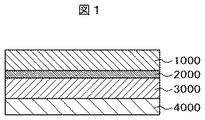
図1は、本発明による3次元表示装置の断面図模式図である。図1に示す装置は、液晶表示パネル3000によって形成された画像を液晶パララックスバリアパネル1000を用いて3次元画像を視認できる構成となっている。液晶パララックスバリアパネル(以後パララックスバリアパネルという)1000と液晶表示パネル3000は透明接着部材2000によって接着している。
FIG. 1 is a schematic cross-sectional view of a three-dimensional display device according to the present invention. The apparatus shown in FIG. 1 is configured such that an image formed by the liquid
液晶表示装置は、自分では発光しないので、液晶表示パネル3000の背面にバックライト4000が配置されている。バックライト4000は光源の他、導光板、拡散板、場合によっては、光の利用効率を向上させるためのプリズムシート等の光学部品を含んでいる。
Since the liquid crystal display device does not emit light by itself, a
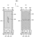
図2はパララックスバリア方式の3次元画像表示の原理を示す断面図である。バリアパターン600に形成されたバリア領域610と開口領域620によって、右眼は表示装置800に形成された右眼用の画像のみを認識し、左眼は左眼用の画像のみを認識することによって、人間は、3次元画像を認識することが出来る。
FIG. 2 is a cross-sectional view showing the principle of parallax barrier 3D image display. By the
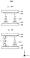
本発明では、表示装置として、IPS方式の液晶表示パネルを用いる。IPS方式の液晶表示パネルは画面を視る角度を大きくしても画像の表示品質が劣化しないという特徴を有する。図3(a)および(b)は、IPS方式の液晶表示パネルの代表的な画素構造を示す平面図である。図3(a)および(b)において、映像信号線202と走査線201に囲まれた領域に画素が形成されている。
In the present invention, an IPS liquid crystal display panel is used as the display device. The IPS liquid crystal display panel has a feature that the display quality of an image does not deteriorate even when the angle at which the screen is viewed is increased. 3A and 3B are plan views showing a typical pixel structure of an IPS liquid crystal display panel. 3A and 3B, pixels are formed in a region surrounded by the
図3(a)は、縦方向にスリット204を有する画素電極203が形成され、その下の図示しない層間絶縁膜を介して平面状にコモン電極205が形成されている。画素電極203には、映像信号線202からTFT207およびTFTのソース電極と接続するスルーホール206を介して映像信号が供給される。TFT207は、走査線201から分岐したゲート電極によってスイッチングされる。
In FIG. 3A, a
図3(a)において、画素電極203に映像信号線202から電圧が供給されるとコモン電極205との間に電気力線が発生するが、この電気力線は、一旦液晶層をとおり、画素電極203に形成されたスリット204あるいは画素電極203の端部を通って画素電極203より下方に形成されたコモン電極205に達する。画素電極203から出た電気力線の横電界成分、すなわち、基板の主面と平行な電界成分によって、液晶層中の液晶分子300が回転する。IPS方式の液晶表示装置では、この液晶分子300の回転の量によって、画素毎に、画素を透過するバックライトからの光の量を制御して画像を形成する。
In FIG. 3A, when a voltage is supplied to the
液晶分子300は、画素電極203の上に形成された配向膜によって初期配向を受けており、この初期配向の向きからの回転量によって光の透過率を制御している。以後配向膜に形成された液晶分子300に対する初期配向の向きを配向膜の配向軸と呼ぶ。配向膜に対する配向処理は、ラビング配向あるいは偏光紫外線を用いた光配向等が用いられる。図3(a)における配向軸は、画素電極203のスリット204の長手方向、すなわち、図3のy方向に対して8度程度傾いている。図3(a)における液晶分子300の長軸の傾きが初期配向の向き、すなわち、配向軸を示している。これは、液晶分子300が横電界を受けたさいに、画素内の全ての液晶分子に対して同一方向に回転させるためである。このように、画素内において、全ての液晶分子が同一方向に回転するような構成をシングルドメインと呼んでいる。以後、図3(a)の画素構造を縦櫛歯と呼ぶ。
The
図3(b)の場合も図3(a)の場合もIPS方式としての基本動作原理は同じである。図3(b)が図3(a)と異なる点は、画素電極203の形状と配向膜に形成された液晶分子300に対する配向軸方向である。図3(b)においては、画素電極203に形成されたスリット204の向きが横方向であり、かつ、スリット204が中央部において屈曲している。また、図3(b)における配向膜の配向軸は、走査線の方向、すなわち、図3のx方向と平行である。図3(b)において、液晶分子300の長軸方向が初期配向の向きである。なお、図3(a)、図3(b)において、初期配向の向きをわかりやすくするために、液晶分子を大きく記載しているが、実際には、液晶分子は視認不可能なほど小さい。
The basic operation principle of the IPS system is the same in both the case of FIG. 3B and the case of FIG. FIG. 3B is different from FIG. 3A in the shape of the
図3(b)の画素構造では、画素電極203におけるスリット204は水平方向である配向軸に対して画素の右側と左側において、傾きが異なっている。したがって、画素電極203に電圧が印加されると、液晶分子300の回転する方向が画素の左側と右側において異なる。これによって、液晶表示パネルの視野角特性をより均一にすることが出来る。このように、画素内において、液晶分子300の回転方向が複数存在する場合をマルチドメインと呼んでいる。マルチドメインは視野角特性を改良することが出来るが、ドメインの境界において、光を透過しない領域が発生し、この分、画素の透過率が小さくなる。図3(b)においては、スリット204の屈曲部を結ぶ画素の縦中央線付近がこの境界に該当する。以後図3の画素電極構造を横櫛歯と呼ぶ。
In the pixel structure of FIG. 3B, the
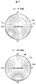
図4は液晶パララックスバリアパネルの動作原理を示す断面図である。図4(a)も図4(b)もTN(Twisted Nematic)方式の液晶パネルである。図4(a)において、対向基板50には対向電極55が平面べたで形成され、バリアパネル60には、所定のピッチでストライプ状のバリア電極65が紙面垂直方向に延在している。図4(a)は、対向電極55とバリア電極65との間に電圧が印加されていない状態であり、液晶表示パネルからの光は変調を受けない。したがって、この場合は、2次元画素が表示される。
FIG. 4 is a cross-sectional view showing the operation principle of the liquid crystal parallax barrier panel. FIG. 4A and FIG. 4B are TN (Twisted Nematic) type liquid crystal panels. 4A, the
図4(b)は同じパララックスバリアパネルのバリア電極65に対して1つおきに電圧を印加した場合である。バリア電極65に電圧が印加された領域は光が遮光され、バリア電極に電圧が印加されない領域は光が透過する。これによって、パララックスバリアパネル主面から見ると、ストライプ状の遮光領域とストライプ状の開口領域が交互に形成されて見える。
FIG. 4B shows the case where every other voltage is applied to the
本発明は、パララックスバリアパネルにTN方式の液晶パネルを用い、表示装置にIPS方式の液晶表示パネルを用いるものである。液晶表示パネルにいわゆるe−modeを用いるかo−modeを用いるかによって、液晶表示パネルの配向軸方向、および、液晶表示パネルに貼り付けられる偏光板の透過軸方向が異なってくる。また、画素電極が横櫛歯の場合と縦櫛歯の場合とでも、液晶表示パネルの配向軸方向、および、液晶表示パネルに貼り付けられる偏光板の透過軸方向が異なってくる。したがって、e−modeを使用するかo−modeを使用するか、画素電極に縦櫛歯を使用するか横櫛歯を使用するかによって、4つの組み合わせが存在する。 The present invention uses a TN liquid crystal panel as a parallax barrier panel and an IPS liquid crystal display panel as a display device. Depending on whether a so-called e-mode or o-mode is used for the liquid crystal display panel, the alignment axis direction of the liquid crystal display panel and the transmission axis direction of the polarizing plate attached to the liquid crystal display panel are different. In addition, the alignment axis direction of the liquid crystal display panel and the transmission axis direction of the polarizing plate attached to the liquid crystal display panel differ depending on whether the pixel electrode is a horizontal comb tooth or a vertical comb tooth. Therefore, there are four combinations depending on whether e-mode or o-mode is used, and vertical or horizontal comb teeth are used for pixel electrodes.
図5は、画素電極203に縦櫛歯を使用した場合であり、図5(a)がe−mode、図5(b)がo−modeの場合である。図5(a)および図5(b)において、液晶表示パネルを構成するTFT基板20の配向軸21とカラーフィルタ基板30の配向軸31は同じ方向のy方向である。実際には液晶表示パネルの配向軸はy方向に対して8度程度傾いているが、図では、y方向として表している。
FIG. 5 shows a case where vertical comb teeth are used for the
図5(a)はe−modeであるから、TFT基板20の下に貼り付けられる第1の偏光板10の透過軸11はTFT基板20の配向軸方向21と直角方向、すなわち、x方向である。また、カラーフィルタ基板30の上に貼り付けられる第2の偏光板40の透過軸31は、液晶表示パネルのカラーフィルタ基板30の配向軸方向31と同じy方向である。パララックスバリアパネルを構成する対向基板50の配向軸方向51は、第2の偏光板40の透過軸方向41と同じy方向であり、バリア基板60の配向軸方向61はx方向となっている。パララックスバリアパネルはTN方式の液晶表示装置を用いているからである。バリア基板60の外側に貼り付けられる第3の偏光板70の透過軸71は、バリアパネルの配向軸方向61と同じx方向である。
Since FIG. 5A is an e-mode, the
図5(b)はo−modeであるから、TFT基板20の下に貼り付けられる第1の偏光板10の透過軸11はTFT基板20の配向軸方向21と平行方向、すなわち、y方向である。また、カラーフィルタ基板30の上に貼り付けられる第2の偏光板40の透過軸41は、液晶表示パネルのカラーフィルタ基板30の配向軸方向31と直角方向であるx方向である。パララックスバリアパネルを構成する対向基板50の配向軸方向51は、第2の偏光板40の透過軸方向41と同じx方向であり、バリア基板60の配向軸方向61はy方向となっている。パララックスバリアパネルはTN方式の液晶表示装置を用いているからである。バリア基板60の外側に貼り付けられる第3の偏光板70の透過軸71は、バリア基板60の配向軸方向61と同じy方向である。
Since FIG. 5B is o-mode, the
図6は、画素電極203に横櫛歯を使用した場合であり、図6(a)がe−mode、図6(b)がo−modeの場合である。図6(a)および図6(b)において、液晶表示パネルを構成するTFT基板20の配向軸21とカラーフィルタ基板30の配向軸31は同じ方向のx方向である。
FIG. 6 shows a case where horizontal comb teeth are used for the
図6(a)はe−modeであるから、TFT基板20の下に貼り付けられる第1の偏光板10の透過軸11はTFT基板20の配向軸方向21と直角方向、すなわち、y方向である。また、カラーフィルタ基板30の上に貼り付けられる第2の偏光板40の透過軸41は、液晶表示パネルのカラーフィルタ基板30の配向軸方向31と同じx方向である。パララックスバリアパネルを構成する対向基板50の配向軸方向51は、第2の偏光板40の透過軸方向41と同じx方向であり、バリア基板60の配向軸方向61はy方向となっている。パララックスバリアパネルはTN方式の液晶表示装置を用いているからである。バリア基板60の外側に貼り付けられる第3の偏光板70の透過軸71は、バリア基板60の配向軸方向61と同じy方向である。
Since FIG. 6A is an e-mode, the
図6(b)はo−modeであるから、TFT基板20の下に貼り付けられる第1の偏光板10の透過軸11はTFT基板20の配向軸方向21と平行方向、すなわち、x方向である。また、カラーフィルタ基板30の上に貼り付けられる第2の偏光板40の透過軸41は、液晶表示パネルのカラーフィルタ基板30の配向軸方向31と直角方向であるy方向である。パララックスバリアパネルを構成する対向基板50の配向軸方向51は、第2の偏光板40の透過軸方向41と同じy方向であり、バリア基板60の配向軸方向61はx方向となっている。パララックスバリアパネルはTN方式の液晶表示装置を用いているからである。バリア基板60の外側に貼り付けられる第3の偏光板70透過軸71は、バリア基板60の配向軸と同じx方向である。
Since FIG. 6B is an o-mode, the
ところで、TN方式の液晶表示パネルは、視野角が問題である。すなわち、斜め方向が見た場合、画面のコントラストが低下したり、色度が変化したりする。したがって、パララックスバリアパネルとしてTN方式の液晶パネルを使用する場合、視野角が問題となる。TN液晶パネルでは、配向膜の配向処理はラビング方式が使用される。TN液晶パネルにおける視野角はラビング方向、すなわち、配向軸と45度方向が視野角が最も広くなる方向であり且つ対称となる。 By the way, the viewing angle of the TN liquid crystal display panel is a problem. That is, when the oblique direction is viewed, the contrast of the screen is lowered or the chromaticity is changed. Accordingly, when a TN liquid crystal panel is used as the parallax barrier panel, the viewing angle becomes a problem. In the TN liquid crystal panel, a rubbing method is used for the alignment treatment of the alignment film. The viewing angle in the TN liquid crystal panel is the rubbing direction, that is, the direction where the viewing angle is the widest with respect to the alignment axis and the direction of 45 degrees is symmetrical.
図5あるいは図6においては、TN液晶パネルにおける対向基板50あるいはバリア基板60の配向軸は、液晶表示パネルとして使用するIPS方式の液晶表示パネルにおけるTFT基板20あるいはカラーフィルタ基板30の配向軸と一致させているので、配向軸方向は、x方向あるいはy方向となり、視野角が広く且つ対称となる領域は、x方向あるいはy方向に対して45度の方向である。
In FIG. 5 or FIG. 6, the alignment axis of the
このような場合のコントラスト分布を示したものが図7(a)である。図7(a)において、曲線は、コントラストの等高線である。図7(a)において、TMで示した等高線がコントラストが最も大きい範囲である。図7(a)において、水平方向、すなわち、0度−180度におけるコントラストが大きい部分THは限られた範囲である。 FIG. 7A shows the contrast distribution in such a case. In FIG. 7A, the curve is a contour line of contrast. In FIG. 7A, the contour line indicated by TM is the range where the contrast is the largest. In FIG. 7A, the portion TH having a large contrast in the horizontal direction, that is, in the range of 0 ° to 180 ° is a limited range.
しかし、パララックスバリア方式の液晶表示装置では、視線がバリアパターンの延在方向に対して直角方向、すなわち、x方向に移動した場合が問題となる。本発明においては、パララックスバリアパネルにおける対向基板およびバリア基板の配向軸をx方向に対し45度方向にすることによって、バリアパターンの延在方向に対して直角方向、すなわち、x方向の視野角を増大させるものである。 However, in the parallax barrier type liquid crystal display device, a problem occurs when the line of sight moves in a direction perpendicular to the extending direction of the barrier pattern, that is, in the x direction. In the present invention, the orientation axis of the counter substrate and the barrier substrate in the parallax barrier panel is set to 45 degrees with respect to the x direction, so that the viewing angle in the direction perpendicular to the barrier pattern extending direction, that is, the x direction is obtained. Is to increase.
図7(b)は、本発明におけるパララックスバリアパネルの視野角特性を示す等高線分布である。図7(b)において、コントラストの最も大きい範囲の等高線をTMで示している。0度−180度におけるコントラストが大きい部分THは、図7(a)の場合に比較して拡大している。これによって、パララックスバリア方式において、視線が移動した場合のコントラストの低下や色度の変化を緩和することができる。 FIG. 7B is a contour distribution showing the viewing angle characteristics of the parallax barrier panel according to the present invention. In FIG. 7B, the contour lines in the range with the largest contrast are indicated by TM. The portion TH having a large contrast at 0 degrees to 180 degrees is enlarged as compared with the case of FIG. Thereby, in the parallax barrier method, it is possible to mitigate a decrease in contrast and a change in chromaticity when the line of sight moves.
図8は、画素電極が横櫛歯でe−modeの場合における第1乃至第3偏光板の透過軸、TFT基板20、カラーフィルタ基板30、パララックスバリアパネルにおける対向基板50、バリア基板60の配向軸の関係を示す模式図である。第1偏光板10と第2偏光板40の透過軸、TFT基板20、カラーフィルタ基板30の配向軸の関係は、e−modeであるかo−modeであるかによって変化する。図8における重要な点は、カラーフィルタ基板30の配向軸方向31あるいは第2偏光板40の透過軸41がパララックスバリアパネルにおける対向基板50の配向軸方向51と一致していない点である。図8では、パララックスバリアパネルの対向基板50およびバリア基板60の配向軸方向51、61をx方向に対して45度傾けるので、パララックスバリア方式の3次元表示装置の水平方向の視野角を向上させることが出来る。この場合の45度は厳密な意味での45度でなくともよい。実用的には、45度±10度であればよい。
FIG. 8 shows the transmission axes of the first to third polarizing plates, the
図9は、実施例1における第1乃至第3偏光板の透過軸、液晶表示パネルおよびパララックスバリアパネルの基板の配向軸の関係を示す表である。図5および図6で説明した構成は比較例として記載されている。実施例1の欄は次のとおりである。実施例1は、画素電極が縦櫛歯、または、横櫛歯の場合、あるいは、動作モードがe−mode、または、o−modeの場合のいずれについても適用することが出来る。実施例1における第1および第2偏光板の透過軸方向、TFT基板およびカラーフィルタ基板の配向軸方向は、比較例と同じである。実施例1は、パララックスバリアパネルにおける対向基板50およびバリア基板60の配向軸51、61、あるいは、第3の偏光板の偏光軸方向71が45度あるいは135度である点で比較例と異なっている。図9において、45度と135度は互いに交換可能である。プラスx方向であれ、マイナスx方向であれ、x方向に対して45度の角度で交差すればよい。以下の図18、図20の表についても同様である。なお、この場合の45度は厳密な意味での45度でなくともよい。実用的には、45度±10度でよい。
FIG. 9 is a table showing the relationship between the transmission axes of the first to third polarizing plates and the alignment axes of the substrates of the liquid crystal display panel and the parallax barrier panel in Example 1. The configuration described with reference to FIGS. 5 and 6 is described as a comparative example. The column of Example 1 is as follows. The first embodiment can be applied to either the case where the pixel electrode is a vertical comb or a horizontal comb, or the case where the operation mode is e-mode or o-mode. The transmission axis directions of the first and second polarizing plates and the alignment axis directions of the TFT substrate and the color filter substrate in Example 1 are the same as those in the comparative example. Example 1 differs from the comparative example in that the orientation axes 51 and 61 of the
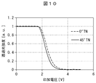
図10は、パララックスバリアパネルにおける対向基板とバリア基板における配向軸を第2あるいは第3偏光板の透過軸と合わせた場合(0度)と、本実施例におけるように、パララックスバリアパネルにおける対向基板とバリア基板における配向軸を第2あるいは第3偏光板の透過軸と45度の角度とした場合における光の透過を比較したものである。図10において、横軸は、対向電極とバリア電極との間の電圧、縦軸はパララックスバリアパネルの透過率である。図10に示すように、パララックスバリアパネルにおける対向基板とバリア基板における配向軸を第2あるいは第3偏光板の透過軸と45度の角度とした場合は、0度とした場合に比較してパララックスバリアパネルの透過率は大きく変化していないことがわかる。この結果から、45度の角度としたとしても光学的には影響がないと言える。 この影響をパララックスバリア方式における正面クロストークと視野角が画面の法線方向から30度の場合におけるクロストークとで比較したものが、図11である。図11では実施例2−4も記載しているが、これらについては、後で説明する。図11において、正面のクロストークは、比較例は0.6%であるのに対し、実施例1では1.5%と、劣化している。一方、法線方向から30度傾いた方向から見た場合のクロストークは、比較例は6%であるのに対し、実施例1では3%と、大幅に向上している。したがって、視野角も考慮した全体的な3次元表示としては、実施例1のほうが向上しているといえる。 FIG. 10 shows a case where the orientation axes of the counter substrate and the barrier substrate in the parallax barrier panel are aligned with the transmission axis of the second or third polarizing plate (0 degree), and in the parallax barrier panel as in this embodiment. This is a comparison of light transmission when the orientation axes of the counter substrate and the barrier substrate are set to an angle of 45 degrees with the transmission axis of the second or third polarizing plate. In FIG. 10, the horizontal axis represents the voltage between the counter electrode and the barrier electrode, and the vertical axis represents the transmittance of the parallax barrier panel. As shown in FIG. 10, when the orientation axis of the counter substrate and the barrier substrate in the parallax barrier panel is an angle of 45 degrees with the transmission axis of the second or third polarizing plate, it is compared with the case where the orientation axis is 0 degree. It can be seen that the transmittance of the parallax barrier panel has not changed significantly. From this result, it can be said that even if the angle is 45 degrees, there is no optical effect. FIG. 11 shows a comparison of this effect between front crosstalk in the parallax barrier method and crosstalk in the case where the viewing angle is 30 degrees from the normal direction of the screen. Although Example 2-4 is also described in FIG. 11, these will be described later. In FIG. 11, the front crosstalk is 0.6% in the comparative example, and deteriorates to 1.5% in the first embodiment. On the other hand, the crosstalk when viewed from a direction inclined by 30 degrees from the normal direction is significantly improved to 6% in Example 1 as compared to 6% in the comparative example. Therefore, it can be said that Example 1 is improved as an overall three-dimensional display considering the viewing angle.
このように、本発明は、パララックスバリアパネルとして使用するTN液晶パネルの視野角を向上させることによって、視線を移動させてもクロストークが大きくなることを防止することに主眼がある。視線の移動に合わせてパララックスバリアの位置を移動させると、視線を移動させた場合におけるクロストークをさらに減少させることが出来る。この場合、まず、視線の移動を感知し、これを表示装置にフィードバックさせる必要がある。 As described above, the present invention is mainly directed to preventing an increase in crosstalk even when the line of sight is moved by improving the viewing angle of a TN liquid crystal panel used as a parallax barrier panel. When the position of the parallax barrier is moved in accordance with the movement of the line of sight, the crosstalk when the line of sight is moved can be further reduced. In this case, first, it is necessary to sense the movement of the line of sight and feed it back to the display device.
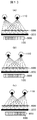
図12は、視線の移動をカメラによって追跡し、このデータを表示装置にフィードバックするシステムを示すブロック図である。以後このシステムをアイトラッキング方式と呼ぶ。図12において、人間の眼110の位置をカメラで測定する。このカメラは、携帯電話等における写真用カメラを使用すれば、特別に専用カメラを用いなくとも、このシステムを適用することが出来る。
FIG. 12 is a block diagram showing a system in which the movement of the line of sight is tracked by a camera and this data is fed back to the display device. Hereinafter, this system is called an eye tracking method. In FIG. 12, the position of the
図12において、カメラで検出した人間の眼110の位置を位置検出器に入力し、位置検出器からバリア制御器にこの信号を入力する。バリア制御器は、バリア基板におけるバリアパターンの位置を制御するための信号を作り、この信号をパララックスバリアパネルを有する3次元表示装置に入力する。
In FIG. 12, the position of the
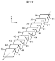
図13は、人間の眼110が移動した場合にも、右眼用の画素と左眼用の画素がクロストークしないように、人間の眼110の移動に合わせてバリアパターン600を移動することを示す模式図である。図13において、人間の眼110はバリアパターン600を介して画素パターン800を視認するので、人間は3次元画像を認識することが出来る。図13は、図13(a)から(c)にかけて人間の眼が紙面に向かって左から右方向に移動していることを示し、それに合わせてバリアパターンが左から右方向に移動している。これによって、右眼用の画素と左眼用の画素のクロストークを防止することができる。
FIG. 13 shows that the
図14は、パララックスバリアパネルにおいてバリアパターン600を移動させるための電極構造を示すものである。図14において、対向基板50には対向電極55が平面状に形成されていることは従来と同じである。一方、バリア基板60におけるバリア電極65は紙面垂直方向に延在するストライプ状である。図14においては、5本のバリア電極65をonすることによってバリア領域を形成し、off状態の5本のバリア電極65に対応して開口領域620が形成されている。バリア領域610の位置を移動させるには、バリア領域610における片側のバリア電極65をoffし、バリア領域610の他の側のバリア電極65をonさせればよい。
FIG. 14 shows an electrode structure for moving the
このように、複数のバリア電極65によってバリア領域610を形成することで、バリア領域610の位置を移動させることが出来、アイトラッキングによるフィードバックをより正確に行うことが出来る。
Thus, by forming the
なお、図14において、バリア電極65がonになっている領域にバリア領域610が形成され、バリア電極65がoffになっている領域に透過領域620が形成されている。また、バリア電極65がonになっている状態は、バリア電極65に電圧が印加されている状態のことである。このバリア領域610の幅あるいは透過領域620の幅が、1画素の幅、すなわち、赤画素(R)、緑画素(G)、青画素(B)のサブピクセルの合計の幅となっている。
In FIG. 14, a
図15は、バリア領域610を複数のバリア電極65によって形成する場合における他の例である。図11の例では、複数に分割されたバリア電極65間に隙間が存在するので、この隙間において、光漏れが発生する危険がある。この光もれは右眼用画像と左眼用画像のクロストークの原因になる。図15は、バリア基板60側において、バリア電極65を絶縁膜を挟んで2層形成し、対向基板50側から見た場合、バリア電極65間に隙間が発生しないようにしている。これによって、バリア領域610における光漏れは、完全に阻止され、光もれによるクロストークの発生を防止することが出来る。
FIG. 15 shows another example when the
図16は、バリア領域610を複数のバリア電極65によって形成する場合におけるさらに他の例である。図16が図15と異なる点は、上層のバリア電極65の間隔がバリア電極65の幅よりも小さく、下層のバリア電極652の幅が、上層のバリア電極65の幅よりも小さいことである。バリア基板60側において、バリア電極65を絶縁膜653を挟んで2層形成し、対向基板50側から見た場合、バリア電極65間に隙間が発生しないようにする目的は図15と同様である。すなわち、上層のバリア電極65と下層のバリア電極652の幅は必ずしも同じ幅である必要は無い。
FIG. 16 shows still another example when the
図16のようなバリア電極65の構成においては、絶縁膜653を挟んで隣同士の上層のバリア電極65と下層のバリア電極652の電圧を同電位とすると動作が容易である。
In the configuration of the
以上のように、本実施例では、パララックスバリアパネルにおける対向基板50とバリア基板60の配向軸51,61が第2偏光板40の透過軸と異なることによるパララックスバリアパネルの透過率の減少、および、正面におけるクロストークの増大等をきたすが、視線が移動した場合に、パララックスバリアパネルの視野角が小さいことによるクロストークの増大等による画質の劣化を抑えることが出来るので、全体としてパララックスバリア方式による3次元表示の表示品質を向上させることが出来る。
As described above, in this embodiment, the transmittance of the parallax barrier panel is reduced due to the fact that the orientation axes 51 and 61 of the
以上のように、バリア電極を複数に分割し、視線に合わせてバリア領域の位置を移動させることによって、よりクロストークの小さい3次元画像を形成することが出来る。また、アイトラッキング方式を用いることによって、パララックスバリアにおいて、視線を移動させた場合にもクロストークを抑え、良好な3次元画像を認識することが出来る。 As described above, it is possible to form a three-dimensional image with smaller crosstalk by dividing the barrier electrode into a plurality of pieces and moving the position of the barrier region in accordance with the line of sight. In addition, by using the eye tracking method, it is possible to suppress crosstalk and recognize a good three-dimensional image even when the line of sight is moved in the parallax barrier.
図17は本発明の第2の実施例を示すパララックスバリア方式3次元表示装置の模式図である。図17が実施例1を示す図8と異なる点は、第2偏光板40とパララックスバリアパネルの対向基板50の間にλ/2位相差板80が配置されていることである。λ/2位相差板80の遅相軸81の角度は、水平方向、すなわち、x軸方向に対して22.5度である。図8に示す実施例1では、図10に示すように、正面透過率が低下する。これに対して、本実施例ではλ/2位相差板80を使用することによって、第2偏光板40を透過した光の偏光方向を回転させるので、パララックスバリアパネルの透過率を向上させることが出来る。その他の構成は図8と同様である。
FIG. 17 is a schematic view of a parallax barrier type three-dimensional display device showing a second embodiment of the present invention. FIG. 17 is different from FIG. 8 showing the first embodiment in that a λ / 2
本実施例も、画素電極が縦櫛歯の場合、横櫛歯の場合、e−mode、o−modeのいずれのシステムにおいても適用することが出来る。図18は、本実施例における第1乃至第3偏光板の透過軸、TFT基板、カラーフィルタ基板、対向基板、バリア基板の配向軸の関係を示す表である。本実施例では、λ/2位相差板を使用したことによって、パララックスバリアパネルの透過率を向上させ、パララックスバリア方式における正面クロストークを抑えることができる。また、パララックスバリア方式における視野角を向上させることが出来るのは、実施例1と同様である。 This embodiment can also be applied to both e-mode and o-mode systems when the pixel electrode is a vertical comb tooth or a horizontal comb tooth. FIG. 18 is a table showing the relationship between the transmission axes of the first to third polarizing plates, the alignment axes of the TFT substrate, the color filter substrate, the counter substrate, and the barrier substrate in this example. In this embodiment, by using the λ / 2 phase difference plate, the transmittance of the parallax barrier panel can be improved and the front crosstalk in the parallax barrier system can be suppressed. The viewing angle in the parallax barrier method can be improved as in the first embodiment.
図11に本実施例におけるクロストークに対する効果を示す。実施例2の正面クロストークは従来例よりも若干悪化しているが、実施例1よりも改善している。また、表示装置の主面に対する法線方向から30度の場合のクロストークは従来例よりも大幅に改善し、実施例1よりもさらに改善している。これによって、パララックスバリア方式の3次元画像表示の表示品質を向上させることが出来る。 FIG. 11 shows the effect on crosstalk in this embodiment. The front crosstalk of Example 2 is slightly worse than that of the conventional example, but is improved over that of Example 1. Further, the crosstalk in the case of 30 degrees from the normal direction to the main surface of the display device is greatly improved as compared with the conventional example, and further improved as compared with the first embodiment. Thereby, the display quality of the 3D image display of the parallax barrier system can be improved.
図19は本発明の第3の実施例を示すパララックスバリア方式の3次元表示装置の模式図である。図19が実施例2を示す図17と異なる点は、パララックスバリアパネルの対向基板50とλ/2位相差板80との間に第4偏光板90が配置されていることである。その他の構成は実施例2を示す図17と同様である。実施例2においては、λ/2位相差板80を用いることによって、第2偏光板40を透過した光の偏光方向を回転させるので、パララックスバリアパネルの透過率を向上させているが、λ/2位相差板80の効果は光の波長ごとに異なる。この点において、色度ごとに効果を見た場合、クロストークに対して十分な効果を得られない場合がある。
FIG. 19 is a schematic diagram of a parallax barrier type three-dimensional display device according to a third embodiment of the present invention. FIG. 19 is different from FIG. 17 showing the second embodiment in that a fourth
本実施例は、λ/2位相差板80の後に、透過軸がパララックスバリアパネルの対向基板50の配向軸方向51と同じ45度の第4偏光板90を用いることによって、対向基板50に入射する光を限定することにより、色度による特性の違いを防止している。本実施例も、画素電極が縦櫛歯の場合、横櫛歯の場合、e−mode、o−modeのいずれのシステムにおいても適用することが出来る。
In this embodiment, a fourth
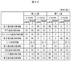
図20は、本実施例における第1乃至第4偏光板の透過軸、TFT基板、カラーフィルタ基板、対向基板、バリア基板の配向軸の関係を示す表である。本実施例では、λ/2位相差板80および第4偏光板90を使用したことによって、実施例1に比較してパララックスバリアパネルの透過率を向上させ、パララックスバリア方式における正面クロストークを抑えることができる。また、パララックスバリア方式における視野角を向上させることが出来るのは、実施例1と同様である。
FIG. 20 is a table showing the relationship among the transmission axes of the first to fourth polarizing plates, the alignment axes of the TFT substrate, the color filter substrate, the counter substrate, and the barrier substrate in this example. In the present embodiment, by using the λ / 2
図11に本実施例におけるクロストークに対する効果を示す。実施例3の正面クロストークは従来例よりも若干悪化しているが、実施例1および2よりも改善している。また、表示装置の主面に対する法線方向から30度の場合のクロストークは従来例よりも大幅に改善し、実施例1および2よりもさらに改善している。これによって、パララックスバリア方式の3次元画像表示の表示品質を向上させることが出来る。 FIG. 11 shows the effect on crosstalk in this embodiment. The front crosstalk of Example 3 is slightly worse than that of the conventional example, but is improved over Examples 1 and 2. Further, the crosstalk in the case of 30 degrees from the normal direction to the main surface of the display device is greatly improved as compared with the conventional example, and further improved as compared with the first and second embodiments. Thereby, the display quality of the 3D image display of the parallax barrier system can be improved.
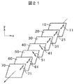
図21は本発明の第4の実施例を示すパララックスバリア方式の3次元表示装置の模式図である。図21が実施例1を示す図8と異なる点は、IPS方式の液晶表示パネルのTFT基板20とカラーフィルタ基板30の配向軸21、31が0度または90度ではなく、45度または135度である点である。これによって、液晶表示パネルとパララックスバリアパネルとの間にλ/2位相差板、あるいは、第4偏光板を配置しなくとも、透過率の減少を防止し、かつ、正面クロストークを軽減することが出来る。また、パララックスバリア方式における視野角を向上させることが出来るのは、実施例1と同様である。ただし、本実施例においては、画素電極の櫛歯電極あるいはスリットの向きを水平方向に対して約45度傾ける必要がある。
FIG. 21 is a schematic view of a parallax barrier type three-dimensional display device showing a fourth embodiment of the present invention. FIG. 21 differs from FIG. 8 showing the first embodiment in that the orientation axes 21 and 31 of the
図22は、本実施例における第1乃至第3偏光板の透過軸、TFT基板、カラーフィルタ基板、パララックスバリアパネルの対向基板、バリア基板における配向軸の関係を示した表である。図22において、45度と135度は互いに交換可能である。例えば、縦櫛歯のe−modeにおいて、第1偏光板の偏光軸は45度で、TFT基板の配向軸は135度となっているが、第1偏光板の偏光軸を135度とし、TFT基板の配向軸を45度としてもよい。 FIG. 22 is a table showing the relationship between the transmission axes of the first to third polarizing plates, the TFT substrate, the color filter substrate, the counter substrate of the parallax barrier panel, and the orientation axes of the barrier substrate in this example. In FIG. 22, 45 degrees and 135 degrees are interchangeable. For example, in the vertical comb-teeth e-mode, the polarization axis of the first polarizing plate is 45 degrees and the orientation axis of the TFT substrate is 135 degrees, but the polarization axis of the first polarizing plate is 135 degrees, and the TFT The orientation axis of the substrate may be 45 degrees.
図11に本実施例におけるクロストークに対する効果を示す。実施例4の正面クロストークは従来例よりも若干悪化しているが、実施例1および2よりも改善している。また、表示装置の主面に対する法線方向から30度の場合のクロストークは従来例よりも大幅に改善し、実施例1および2よりもさらに改善している。 FIG. 11 shows the effect on crosstalk in this embodiment. The front crosstalk of Example 4 is slightly worse than that of the conventional example, but is improved over Examples 1 and 2. Further, the crosstalk in the case of 30 degrees from the normal direction to the main surface of the display device is greatly improved as compared with the conventional example, and further improved as compared with the first and second embodiments.
実施例1乃至3における図9、図18、図20において、画素電極が縦櫛歯の場合、液晶表示パネルのTFT基板あいは対向基板の配向軸は90度となっているが、実際の製品では、液晶分子の回転方向を明確に規定するために90度に対して、±8度程度配向軸方向をずらせている。また、実施例4における配向軸は45度としているが、画素電極の形状がシングルドメインに対応する場合は、実際の製品では、液晶分子の回転方向を明確に規定するために45度に対して、例えば8度程度配向軸方向をずらせている。デスクリネーションの発生を防止するためである。
9, 18, and 20 in
要するに、図9、図18、図20等の表におけるTFT基板あるいはカラーフィルタ基板の配向軸方向である0度、90度、45度、135度等は、必ずしもこの角度に限らず、±10度程度まで許容可能であるということである。 In short, 0 degree, 90 degrees, 45 degrees, 135 degrees, etc., which are the orientation axis directions of the TFT substrate or color filter substrate in the tables of FIG. 9, FIG. 18, FIG. 20, etc. are not necessarily limited to this angle, but ± 10 degrees. It is acceptable to a certain extent.
また、実施例1乃至3では、画素電極が図3(a)に示す縦櫛歯の場合がシングルドメイン、図3(b)に示す横櫛歯の場合がマルチドメインであるとして説明した。しかし、図3(a)および(b)は例であって、縦櫛歯の場合にも、スリットの形状を屈曲させる等することによってマルチドメインとすることが出来る。また、横櫛歯の場合も設計によっては、スリットの形状を屈曲させずに、シングルドメインの画素とすることも出来る。また、マルチドメイン構造の画素も図3(b)の形状にかかわらず、他の形状とすることも出来る。 In the first to third embodiments, the case where the pixel electrode has the vertical comb teeth shown in FIG. 3A is single domain, and the case where the pixel electrode has the horizontal comb teeth shown in FIG. However, FIGS. 3A and 3B are examples, and even in the case of vertical comb teeth, a multi-domain can be obtained by bending the slit shape or the like. In the case of a horizontal comb, depending on the design, a single domain pixel can be formed without bending the slit shape. In addition, the pixels having a multi-domain structure can have other shapes regardless of the shape of FIG.
10…第1偏光板、 11…第1偏光板透過軸、 20…TFT基板、 21…TFT基板配向軸、 30…カラーフィルタ基板、 31…カラーフィルタ基板配向軸、 40…第2偏光板、 41…第2偏光板透過軸、 50…対向基板、 51…対向基板配向軸、 55…対向電極、 60…バリア基板、 61…バリア基板配向軸、 65…バリア電極、 70…第3偏光板、 71…第3偏光板透過軸、 80…λ/2位相差板、 81…λ/2位相差板遅相軸、 90…第4偏光板、 91…第4偏光板透過軸、 100…画素、 110…眼、 201…走査線、 202…映像信号線、 203…画素電極、 204…スリット、 205…コモン電極、 206…スルーホール、 207…TFT、 300…液晶分子、 600…バリアパターン、 610…バリア領域、 620…開口領域、 652…第2バリア電極、 653…絶縁膜、 800…画素パターン、 1000…液晶パララックスバリアパネル、 2000…接着材、 3000…液晶表示パネル、 4000…バックライト
DESCRIPTION OF
Claims (4)
前記パララックスバリアパネルは、第1の数の隣接する前記バリア電極に電圧を印加することによってバリア領域を形成し、前記バリア領域に隣接し、前記第1の数の隣接するバリア電極には電圧を印加しないことによって開口領域を形成し、前記バリア領域と前記開口領域が第2のピッチで形成され、前記電圧を印加する前記バリア電極を変えることによって、前記バリア領域の位置を変えることが出来、
前記TFT基板の下には第1偏光板が配置し、前記カラーフィルタ基板の上には第2偏光板が配置し、前記バリア基板の上には第3偏光板が配置し、
前記対向基板の配向軸方向は、表示画面の水平方向と45度±10度の角度をなし、
前記カラーフィルタ基板の配向軸の方向と前記対向基板の配向軸方向とは、0度±10度であることを特徴とする3次元表示装置。 An IPS liquid crystal display panel having a TFT substrate on which pixel electrodes are formed and a color filter substrate, and a barrier formed with barrier electrodes extending in the first direction and arranged at the first pitch in the second direction A parallax barrier type three-dimensional display device in which a parallax barrier panel, which is a TN type liquid crystal panel having a counter substrate on which a substrate and a counter electrode are formed, is laminated,
The parallax barrier panel forms a barrier region by applying a voltage to a first number of adjacent barrier electrodes, is adjacent to the barrier region, and has a voltage applied to the first number of adjacent barrier electrodes. The barrier region and the opening region are formed at a second pitch, and the position of the barrier region can be changed by changing the barrier electrode to which the voltage is applied. ,
A first polarizing plate is disposed under the TFT substrate, a second polarizing plate is disposed on the color filter substrate, and a third polarizing plate is disposed on the barrier substrate,
The orientation axis direction of the counter substrate forms an angle of 45 ° ± 10 ° with the horizontal direction of the display screen,
3. The three-dimensional display device according to claim 1, wherein an orientation axis direction of the color filter substrate and an orientation axis direction of the counter substrate are 0 degrees ± 10 degrees.
Priority Applications (2)
| Application Number | Priority Date | Filing Date | Title |
|---|---|---|---|
| JP2013238131A JP6207355B2 (en) | 2013-11-18 | 2013-11-18 | 3D display device |
| US14/542,873 US20150138461A1 (en) | 2013-11-18 | 2014-11-17 | Three dimensional display device |
Applications Claiming Priority (1)
| Application Number | Priority Date | Filing Date | Title |
|---|---|---|---|
| JP2013238131A JP6207355B2 (en) | 2013-11-18 | 2013-11-18 | 3D display device |
Publications (3)
| Publication Number | Publication Date |
|---|---|
| JP2015099202A JP2015099202A (en) | 2015-05-28 |
| JP2015099202A5 JP2015099202A5 (en) | 2016-11-04 |
| JP6207355B2 true JP6207355B2 (en) | 2017-10-04 |
Family
ID=53172963
Family Applications (1)
| Application Number | Title | Priority Date | Filing Date |
|---|---|---|---|
| JP2013238131A Active JP6207355B2 (en) | 2013-11-18 | 2013-11-18 | 3D display device |
Country Status (2)
| Country | Link |
|---|---|
| US (1) | US20150138461A1 (en) |
| JP (1) | JP6207355B2 (en) |
Families Citing this family (4)
| Publication number | Priority date | Publication date | Assignee | Title |
|---|---|---|---|---|
| WO2017018332A1 (en) * | 2015-07-29 | 2017-02-02 | シャープ株式会社 | Image display device |
| JP2017173387A (en) * | 2016-03-18 | 2017-09-28 | パナソニックIpマネジメント株式会社 | Display device |
| US10652526B2 (en) * | 2016-04-25 | 2020-05-12 | Sun Yat-Sen University | Three-dimentional display system based on division multiplexing of viewer's entrance-pupil and display method thereof |
| US10503032B2 (en) | 2018-03-30 | 2019-12-10 | Panasonic Liquid Crystal Display Co., Ltd. | Liquid crystal display device |
Family Cites Families (14)
| Publication number | Priority date | Publication date | Assignee | Title |
|---|---|---|---|---|
| WO2006132361A1 (en) * | 2005-06-10 | 2006-12-14 | Sharp Kabushiki Kaisha | Display element and display device |
| US7359105B2 (en) * | 2006-02-07 | 2008-04-15 | Sharp Kabushiki Kaisha | Spatial light modulator and a display device |
| KR20080114310A (en) * | 2007-06-27 | 2008-12-31 | 삼성모바일디스플레이주식회사 | Electronic display device |
| JP2009115834A (en) * | 2007-11-01 | 2009-05-28 | Hitachi Displays Ltd | Liquid crystal display |
| TW201019018A (en) * | 2008-11-04 | 2010-05-16 | Chunghwa Picture Tubes Ltd | Stereoscopic display device |
| JP5634503B2 (en) * | 2010-04-09 | 2014-12-03 | シャープ株式会社 | Active shutter glasses and 3D image recognition system |
| WO2012008408A1 (en) * | 2010-07-12 | 2012-01-19 | シャープ株式会社 | Display device |
| JP5648361B2 (en) * | 2010-08-10 | 2015-01-07 | ソニー株式会社 | Display device |
| JP2012037808A (en) * | 2010-08-10 | 2012-02-23 | Sony Corp | Stereoscopic display device and liquid crystal barrier device |
| JP2012063704A (en) * | 2010-09-17 | 2012-03-29 | Sony Corp | Display device |
| KR101461186B1 (en) * | 2011-07-07 | 2014-11-13 | 엘지디스플레이 주식회사 | Stereoscopic image display device and driving method the same |
| JP5907758B2 (en) * | 2012-03-02 | 2016-04-26 | 株式会社ジャパンディスプレイ | Display device and liquid crystal barrier element |
| GB2508844A (en) * | 2012-12-12 | 2014-06-18 | Sharp Kk | Analogue parallax barrier |
| JP6124587B2 (en) * | 2012-12-27 | 2017-05-10 | 三菱電機株式会社 | Display device |
-
2013
- 2013-11-18 JP JP2013238131A patent/JP6207355B2/en active Active
-
2014
- 2014-11-17 US US14/542,873 patent/US20150138461A1/en not_active Abandoned
Also Published As
| Publication number | Publication date |
|---|---|
| US20150138461A1 (en) | 2015-05-21 |
| JP2015099202A (en) | 2015-05-28 |
Similar Documents
| Publication | Publication Date | Title |
|---|---|---|
| JP5301605B2 (en) | Liquid crystal display | |
| JP5634926B2 (en) | Liquid crystal display | |
| JP6200789B2 (en) | Display device | |
| KR20130018165A (en) | Display device | |
| JP5910470B2 (en) | Display device and driving method thereof | |
| TWI530729B (en) | Image display device and liquid crystal lens | |
| KR102171611B1 (en) | Stereopsis image display device | |
| JP2014160282A (en) | Display device | |
| JP2011169949A (en) | Three-dimensional image display device | |
| JP6207355B2 (en) | 3D display device | |
| KR102144733B1 (en) | Stereopsis image display device | |
| US9316844B2 (en) | 3D display apparatus and method for manufacturing the same | |
| US9759925B2 (en) | Three-dimensional image display apparatus | |
| JP6125027B2 (en) | 3D display device | |
| WO2015060002A1 (en) | Three-dimensional display device | |
| JP2015052624A (en) | Stereoscopic display device | |
| US9709813B2 (en) | Image display device | |
| JP5669945B2 (en) | 3D display device | |
| JP5960224B2 (en) | Liquid crystal display | |
| JP2012226216A (en) | Liquid crystal display device | |
| JP5710696B2 (en) | Display device | |
| KR101873039B1 (en) | Stereoscopic image display device | |
| KR101373932B1 (en) | Polarization glasses type stereoscopic image display |
Legal Events
| Date | Code | Title | Description |
|---|---|---|---|
| A521 | Request for written amendment filed |
Free format text: JAPANESE INTERMEDIATE CODE: A523 Effective date: 20160912 |
|
| A621 | Written request for application examination |
Free format text: JAPANESE INTERMEDIATE CODE: A621 Effective date: 20160912 |
|
| A977 | Report on retrieval |
Free format text: JAPANESE INTERMEDIATE CODE: A971007 Effective date: 20170426 |
|
| A131 | Notification of reasons for refusal |
Free format text: JAPANESE INTERMEDIATE CODE: A131 Effective date: 20170530 |
|
| A521 | Request for written amendment filed |
Free format text: JAPANESE INTERMEDIATE CODE: A523 Effective date: 20170727 |
|
| TRDD | Decision of grant or rejection written | ||
| A01 | Written decision to grant a patent or to grant a registration (utility model) |
Free format text: JAPANESE INTERMEDIATE CODE: A01 Effective date: 20170808 |
|
| A61 | First payment of annual fees (during grant procedure) |
Free format text: JAPANESE INTERMEDIATE CODE: A61 Effective date: 20170905 |
|
| R150 | Certificate of patent or registration of utility model |
Ref document number: 6207355 Country of ref document: JP Free format text: JAPANESE INTERMEDIATE CODE: R150 |
|
| R250 | Receipt of annual fees |
Free format text: JAPANESE INTERMEDIATE CODE: R250 |
|
| R250 | Receipt of annual fees |
Free format text: JAPANESE INTERMEDIATE CODE: R250 |
|
| R250 | Receipt of annual fees |
Free format text: JAPANESE INTERMEDIATE CODE: R250 |
|
| R250 | Receipt of annual fees |
Free format text: JAPANESE INTERMEDIATE CODE: R250 |
|
| R250 | Receipt of annual fees |
Free format text: JAPANESE INTERMEDIATE CODE: R250 |