KR20120018280A - Light barrier device and display unit - Google Patents
Light barrier device and display unit Download PDFInfo
- Publication number
- KR20120018280A KR20120018280A KR1020110080610A KR20110080610A KR20120018280A KR 20120018280 A KR20120018280 A KR 20120018280A KR 1020110080610 A KR1020110080610 A KR 1020110080610A KR 20110080610 A KR20110080610 A KR 20110080610A KR 20120018280 A KR20120018280 A KR 20120018280A
- Authority
- KR
- South Korea
- Prior art keywords
- sub
- liquid crystal
- light
- spacer
- display
- Prior art date
Links
Images


Classifications
-
- G—PHYSICS
- G02—OPTICS
- G02B—OPTICAL ELEMENTS, SYSTEMS OR APPARATUS
- G02B30/00—Optical systems or apparatus for producing three-dimensional [3D] effects, e.g. stereoscopic images
- G02B30/20—Optical systems or apparatus for producing three-dimensional [3D] effects, e.g. stereoscopic images by providing first and second parallax images to an observer's left and right eyes
- G02B30/26—Optical systems or apparatus for producing three-dimensional [3D] effects, e.g. stereoscopic images by providing first and second parallax images to an observer's left and right eyes of the autostereoscopic type
- G02B30/27—Optical systems or apparatus for producing three-dimensional [3D] effects, e.g. stereoscopic images by providing first and second parallax images to an observer's left and right eyes of the autostereoscopic type involving lenticular arrays
-
- G—PHYSICS
- G02—OPTICS
- G02B—OPTICAL ELEMENTS, SYSTEMS OR APPARATUS
- G02B30/00—Optical systems or apparatus for producing three-dimensional [3D] effects, e.g. stereoscopic images
- G02B30/20—Optical systems or apparatus for producing three-dimensional [3D] effects, e.g. stereoscopic images by providing first and second parallax images to an observer's left and right eyes
- G02B30/26—Optical systems or apparatus for producing three-dimensional [3D] effects, e.g. stereoscopic images by providing first and second parallax images to an observer's left and right eyes of the autostereoscopic type
- G02B30/30—Optical systems or apparatus for producing three-dimensional [3D] effects, e.g. stereoscopic images by providing first and second parallax images to an observer's left and right eyes of the autostereoscopic type involving parallax barriers
- G02B30/31—Optical systems or apparatus for producing three-dimensional [3D] effects, e.g. stereoscopic images by providing first and second parallax images to an observer's left and right eyes of the autostereoscopic type involving parallax barriers involving active parallax barriers
-
- G—PHYSICS
- G02—OPTICS
- G02F—OPTICAL DEVICES OR ARRANGEMENTS FOR THE CONTROL OF LIGHT BY MODIFICATION OF THE OPTICAL PROPERTIES OF THE MEDIA OF THE ELEMENTS INVOLVED THEREIN; NON-LINEAR OPTICS; FREQUENCY-CHANGING OF LIGHT; OPTICAL LOGIC ELEMENTS; OPTICAL ANALOGUE/DIGITAL CONVERTERS
- G02F1/00—Devices or arrangements for the control of the intensity, colour, phase, polarisation or direction of light arriving from an independent light source, e.g. switching, gating or modulating; Non-linear optics
- G02F1/01—Devices or arrangements for the control of the intensity, colour, phase, polarisation or direction of light arriving from an independent light source, e.g. switching, gating or modulating; Non-linear optics for the control of the intensity, phase, polarisation or colour
- G02F1/13—Devices or arrangements for the control of the intensity, colour, phase, polarisation or direction of light arriving from an independent light source, e.g. switching, gating or modulating; Non-linear optics for the control of the intensity, phase, polarisation or colour based on liquid crystals, e.g. single liquid crystal display cells
- G02F1/133—Constructional arrangements; Operation of liquid crystal cells; Circuit arrangements
- G02F1/1333—Constructional arrangements; Manufacturing methods
- G02F1/1335—Structural association of cells with optical devices, e.g. polarisers or reflectors
- G02F1/133524—Light-guides, e.g. fibre-optic bundles, louvered or jalousie light-guides
-
- G—PHYSICS
- G02—OPTICS
- G02F—OPTICAL DEVICES OR ARRANGEMENTS FOR THE CONTROL OF LIGHT BY MODIFICATION OF THE OPTICAL PROPERTIES OF THE MEDIA OF THE ELEMENTS INVOLVED THEREIN; NON-LINEAR OPTICS; FREQUENCY-CHANGING OF LIGHT; OPTICAL LOGIC ELEMENTS; OPTICAL ANALOGUE/DIGITAL CONVERTERS
- G02F1/00—Devices or arrangements for the control of the intensity, colour, phase, polarisation or direction of light arriving from an independent light source, e.g. switching, gating or modulating; Non-linear optics
- G02F1/01—Devices or arrangements for the control of the intensity, colour, phase, polarisation or direction of light arriving from an independent light source, e.g. switching, gating or modulating; Non-linear optics for the control of the intensity, phase, polarisation or colour
- G02F1/13—Devices or arrangements for the control of the intensity, colour, phase, polarisation or direction of light arriving from an independent light source, e.g. switching, gating or modulating; Non-linear optics for the control of the intensity, phase, polarisation or colour based on liquid crystals, e.g. single liquid crystal display cells
- G02F1/133—Constructional arrangements; Operation of liquid crystal cells; Circuit arrangements
- G02F1/1333—Constructional arrangements; Manufacturing methods
- G02F1/1347—Arrangement of liquid crystal layers or cells in which the final condition of one light beam is achieved by the addition of the effects of two or more layers or cells
-
- G—PHYSICS
- G02—OPTICS
- G02F—OPTICAL DEVICES OR ARRANGEMENTS FOR THE CONTROL OF LIGHT BY MODIFICATION OF THE OPTICAL PROPERTIES OF THE MEDIA OF THE ELEMENTS INVOLVED THEREIN; NON-LINEAR OPTICS; FREQUENCY-CHANGING OF LIGHT; OPTICAL LOGIC ELEMENTS; OPTICAL ANALOGUE/DIGITAL CONVERTERS
- G02F2203/00—Function characteristic
- G02F2203/62—Switchable arrangements whereby the element being usually not switchable
Abstract
Description
본 발명은 입체적 표시가 가능한 표시 장치 및 그러한 표시 장치에 이용하는 광 배리어 소자(light barrier device)에 관한 것이다.BACKGROUND OF THE
입체적 표시를 실현하는 표시 장치, 즉, 입체적 표시 장치(stereoscopic display unit)가 주목받고 있다. 입체적 표시에서는 우안용 영상 및 좌안용 영상이 표시된다. 이러한 좌안 및 우안용 영상은 시차(parallax)를 생성하므로, 즉, 이러한 영상들은 상이한 시점(eyepoint)들로부터 보는 것이므로, 이러한 영상들은 관찰자가 그 또는 그녀의 좌우의 눈으로 영상들을 제각기 볼 때 깊이를 갖는 3차원적으로 보여진다. 3개 이상의 시차를 갖는 영상을 표시하는 다른 유형의 표시 장치도 개발되었으며, 그럼으로써 더 자연스럽게 3차원적으로 보이는 영상을 관찰자에게 제공할 수 있다.Display devices that realize stereoscopic display, that is, stereoscopic display units, have attracted attention. In the stereoscopic display, the right eye image and the left eye image are displayed. Since these left and right eye images produce parallax, i.e., these images are viewed from different eyepoints, these images show depth when the viewer views the images with his or her left and right eyes, respectively. It is shown three-dimensionally. Other types of display devices have been developed for displaying images with three or more parallaxes, thereby providing a more natural three-dimensionally visible image to the viewer.
그러한 입체적 표시 장치는 주로 2개의 유형으로 되어 있는데, 한 유형은 전용 안경을 사용하는 것이고, 다른 유형은 그러한 안경을 사용하지 않는 것이다. 그러나, 관찰자들은 흔히 그러한 전용 안경을 사용하는 것을 번거롭게 느끼므로, 안경을 사용하지 않는 유형이 인기가 있다. 그러한 전용 안경을 사용하지 않는 표시 장치는 렌티큘라(lenticular) 렌즈에 기초한 것과 시차 배리어(parallax barrier)에 기초한 것 등을 포함한다.Such stereoscopic display devices are mainly of two types, one type using dedicated glasses, and the other type not using such glasses. However, observers often find it cumbersome to use such dedicated glasses, so the type without glasses is popular. Display devices not using such dedicated glasses include those based on lenticular lenses, those based on parallax barriers, and the like.
특히 시차 배리어에 기초한 표시 장치에서는, 예를 들어 LCD(liquid crystal display)를 이용하여 표시하기 위해 위와 같은 좌안 및 우안용 영상들이 공간적으로 분할되며, 그 표시면에는 소정의 배리어가 제공된다(예를 들어, 일본 미심사 특허출원 공보 3-119889호 참조).In particular, in a display device based on a parallax barrier, the above left and right eye images are spatially divided for display using, for example, a liquid crystal display (LCD), and a predetermined barrier is provided on the display surface (e.g., For example, see Japanese Unexamined Patent Application Publication No. 3-119889.
그러한 배리어는 일반적으로 빛을 투과 또는 차단하기 위한 복수의 개폐부(open/close section)를 포함한다. 예를 들어, 투과 상태에서의 개폐부 즉, 투광부(light-passing section)와 차단 상태에서의 개폐부 즉, 차광부(light-blocking section)의 교번적 배치에 의해 표시 영상들이 다양한 시점 방향으로 분리된다. 기존의 그러한 배리어는 전극을 거쳐서 액정층을 밀봉하는 2장의 기판을 포함하는 것 즉, 액정 셀이다. 예를 들어, 기판들 중 한 쪽에 있는 전극이 복수의 서브 전극으로 분할된다. 이러한 서브 전극들은 제각기 전압 공급이 가능하고, 서브 전극들의 각각에 대응하는 각각의 영역은 개폐부로서 기능한다. 그러한 배리어에서는, 위에서 설명한 액정층의 두께(셀 갭(cell gap))를 제어할 목적으로 스페이서(spacer)가 2장의 기판 사이에 삽입되어 제공된다.Such barriers generally include a plurality of open / close sections for transmitting or blocking light. For example, the display images are separated in various view directions by alternating arrangement of the opening / closing part in the transmissive state, that is, the light-passing section and the light-blocking section in the blocking state. . Such a conventional barrier is one comprising two substrates for sealing a liquid crystal layer via an electrode, that is, a liquid crystal cell. For example, an electrode on one of the substrates is divided into a plurality of sub electrodes. These sub-electrodes are each capable of supplying a voltage, and each region corresponding to each of the sub-electrodes functions as an opening and closing part. In such a barrier, a spacer is provided between two substrates for the purpose of controlling the thickness (cell gap) of the liquid crystal layer described above.
한편, 근년에는, 위와 같은 입체시(stereoscopic viewing)용 표시장치가 대형화 할 것으로 예상되고 있다. 그와 같은 표시 장치에서는, 배리어도 대형화 할 것으로 예상된다. 그러나, 그러한 대형 배리어를 제작하기 위해서는, 생각대로 셀 갭을 유지하기 위해, 위에서 설명한 바와 같은 스페이서가 복수의 위치에 배치되어야 할 것으로 예상된다.On the other hand, in recent years, it is expected that such a stereoscopic viewing display device will be enlarged. In such a display device, the barrier is also expected to be enlarged. However, in order to fabricate such large barriers, it is expected that spacers as described above must be placed in multiple positions in order to maintain the cell gap as desired.
여기에서 문제는, 액정층에 대한 전압 공급을 위한 전극이 위에서 설명한 바와 같이 복수의 서브 전극으로 분할되므로, 서브 전극의 가장자리(edge)에 의해 액정층이 영향을 받아서 프린지 필드(fringe field)가 발생된다는 것이다. 그러므로, 스페이서가 어떤 임의의 위치에든 배치되면, 일부의 위치에서는, 프린지 필드의 영향으로 인해 액정 배향이 흐트러진다. 그러한 배향의 혼란은, 노멀리 화이트 모드(normally-white mode)에서, 흑색 표시(black display) 동안에 예를 들어, 비균일적 광 누출 즉, 스페이서들이 배치된 에리어(area) 및 그 근방이 거기를 통한 빛의 투과로 인해 잔여 에리어보다 더 희끄무리하게 보이는 현상의 원인으로 된다. 그와 같이, 어떤 국소 영역과 잔여 영역 사이에서 광 투과율이 변하는 현상을 일으키는 문제가 있다(이하, 단순하게 "광 얼룩(light unevenness)"이라고 지칭함).The problem here is that the electrode for supplying the voltage to the liquid crystal layer is divided into a plurality of sub-electrodes as described above, so that the fringe field is generated by the liquid crystal layer being affected by the edges of the sub-electrodes. It is. Therefore, if the spacer is disposed at any arbitrary position, at some positions, the liquid crystal alignment is disturbed due to the influence of the fringe field. Such disorientation of orientation is that, in a normally-white mode, during a black display, for example, a non-uniform light leak, i. The transmission of light through causes the phenomenon to appear whitish than the remaining area. As such, there is a problem of causing a change in the light transmittance between a certain local area and the remaining area (hereinafter simply referred to as "light unevenness").
그래서, 광 얼룩의 발생을 방지할 수 있는 광 배리어 소자 및 입체시용 표시장치를 제공하는 것이 양호하다.Therefore, it is desirable to provide a light barrier element and a stereoscopic display device capable of preventing the occurrence of light spots.
본 발명의 한 실시예에 따른 광 배리어 소자는, 한 쌍의 기판 사이에 밀봉되어 제각기 빛이 투과하게 하거나 차단되게 하는 복수의 서브 영역(sub-region)을 포함하는 액정층, 및 한 쌍의 기판 사이에서 서브 영역 사이의 경계 영역 이외의 영역에 제각기 제공된 스페이서들을 포함한다.An optical barrier device according to an embodiment of the present invention includes a liquid crystal layer including a plurality of sub-regions sealed between a pair of substrates to allow light to pass through or blocked, respectively, and a pair of substrates. And spacers provided respectively in regions other than the boundary region between the subregions.
본 발명의 한 실시예에 따른 표시 장치는 위에서 설명한 본 발명의 실시예에 따른 광 배리어 소자 및 표시부를 포함한다.The display device according to the exemplary embodiment of the present invention includes the light barrier device and the display unit according to the exemplary embodiment of the present invention described above.
본 발명의 실시예에 따른 광 배리어 소자에서는, 제각기 빛이 투과하게 하거나 차단되게 하는 복수의 서브 영역을 포함하는 액정층이 한 쌍의 기판 사이에 밀봉되어 있고, 스페이서는 한 쌍의 기판 사이에서 서브 영역 사이의 경계 영역 이외의 영역에 제각기 제공된다. 서브 영역들에는 흔히 전극이 제각기 제공되며, 예를 들어 전극의 가장자리의 영향으로 인해, 서브 전극 사이의 경계 부분은 액정층에서의 배향의 혼란을 겪기 쉽다. 그러한 경계 부분에 스페이서가 배치되면, 스페이서 주변의 에리어는 그 근방에서의 배향의 더 큰 혼란을 겪기 쉽다. 위에서 설명했듯이, 서브 영역 사이의 경계 부분에 있지 않게 스페이서를 제공함으로써 즉, 서브 영역 사이의 경계 영역 이외의 영역에 스페이서를 제공함으로써, 그러한 배향의 혼란으로 인한 투과율의 어떤 국소적 변화든 방지되는 것이 양호하며, 즉, 스페이서 주변의 에리어가 그 곳을 통한 너무 많은 광 누출로 인해 흑색 표시 동안에 잔여 에리어보다 더 희끄무리하게 보이는 현상이 방지되는 것이 양호하다.In an optical barrier device according to an embodiment of the present invention, a liquid crystal layer including a plurality of sub-regions, each of which allows light to pass through or is blocked, is sealed between a pair of substrates, and a spacer is provided between the pair of substrates. Each is provided in an area other than the boundary area between the areas. The subregions are often provided with respective electrodes, for example due to the influence of the edges of the electrodes, the boundary portions between the sub-electrodes are susceptible to disorder of the orientation in the liquid crystal layer. If a spacer is placed at such a boundary, the area around the spacer is likely to experience greater confusion of orientation at its near-degrees. As explained above, by providing a spacer not at the boundary between the subregions, i.e. by providing the spacer at a region other than the boundary region between the subregions, it is possible to prevent any local changes in the transmittance due to such orientation disturbances. It is good to prevent the phenomenon that the area around the spacer appears whitish than the remaining area during black display due to too much light leakage therethrough.
본 발명의 실시예에 따른 광 배리어 소자에서는, 액정층이 한 쌍의 기판 사이에 밀봉되며, 액정층은 제각기 빛이 투과하게 하거나 차단되게 하는 복수의 서브 영역을 포함하고, 서브 영역 사이의 경계 영역 이외의 영역에 스페이서들이 제공된다. 그러므로, 예를 들어, 흑색 표시 동안의 광 누출과 같은 스페이서의 설치로 인한 투과율의 어떤 변화든 방지될 수 있으므로, 어떤 광 얼룩의 발생이든 충분히 방지되게 한다.In an optical barrier device according to an embodiment of the present invention, a liquid crystal layer is sealed between a pair of substrates, and the liquid crystal layer includes a plurality of sub-regions, each of which allows light to pass through or is blocked, and a boundary region between the sub-regions. Spacers are provided in other regions. Therefore, any change in transmittance due to the installation of a spacer such as light leakage during black display, for example, can be prevented, so that any occurrence of light spots is sufficiently prevented.
앞서의 개략적인 설명 및 다음의 상세한 설명은 예시적인 것이며, 청구범위에 기재된 바와 같은 기술에 대한 상세한 설명을 제공하려는 것임을 알아야 한다.It should be understood that the foregoing general description and the following detailed description are exemplary and intended to provide a detailed description of the technology as set forth in the claims.
수반하는 도면은 본 발명에 대해 상세하게 이해하게 하기 위해 포함되며, 이 명세서의 일부를 이루도록 통합된다. 도면은 실시예를 도시하며, 명세서와 함께 이 기술의 원리를 설명하는 작용을 한다.
도 1은 본 발명의 실시예에서의 입체적 표시 장치의 예시적 구성을 도시하는 블록도이다.
도 2a 및 2b는 제각기 도 1의 입체적 표시 장치의 예시적 구성을 도시하는 설명도이다.
도 3은 도 1의 표시부의 예시적 구성 및 그 표시 구동부의 예시적 구성을 도시하는 설명도이다.
도 4a 및 4b는 제각기 도 3의 화소 회로의 예시적 구성 및 화소의 예시적 단면 구성을 도시하는 설명도이다.
도 5는 도 1의 액정 배리어에서의 개폐부의 예시적 구성을 도시하는 설명도이다.
도 6a 및 6b는 제각기 도 1의 액정 배리어의 예시적 단면 구성 및 평면도에서의 그 것의 예시적 구성을 도시하는 모식도이다.
도 7a 및 7b는 제각기 도 1의 액정 배리어의 투과 상태에서의 액정층의 예시적 배향 및 그 차단 상태에서의 액정층의 예시적 배향을 도시하는 설명도이다.
도 8은 입체적 표시를 위한 도 1의 액정 배리어의 예시적 동작을 도시하는 모식도이다.
도 9a 내지 9c는 제각기 도 1의 표시부의 예시적 동작 및 그 액정 배리어의 예시적 동작을 도시하는 모식도이다.
도 10a 및 10b는 제각기 도 1의 표시부의 예시적 동작 및 그 액정 배리어의 예시적 동작을 도시하는 다른 모식도이다.
도 11a 및 11b는 제각기 비교예에서의 액정 배리어의 예시적 단면 구성 및 평면도에서의 액정 배리어의 예시적 구성을 도시하는 모식도이다.
도 12a 및 12b는 비교예에서의 스페이서 배치와 구성요소 치수 및 예 1에서의 스페이서 배치와 구성요소 치수를 제각기 도시하는 모식도이다.
도 13a 및 13b는 제각기 흑색 표시 동안의 전극 경계 및 그 근방에서의 등전위 분포(스페이서가 없는)를 도시하는 특성도이다.
도 14a 및 14b는 제각기 비교예에서 흑색 표시 동안의 등전위 분포(전극 경계 부분에서의 스페이서에 따른)를 도시하는 특성도이다.
도 15a 및 15b는 제각기 예 1에서 흑색 표시 동안의 등전위 분포(전극 사이의 비경계 부분에서의 스페이서에 따른)를 도시하는 특성도이다.
도 16a 및 16b는 변형례에서의 액정 배리어의 예시적 단면 구성 및 평면도에서의 액정 배리어의 예시적 구성을 제각기 도시하는 모식도이다.
도 17은 예 2에서의 스페이서 배치 및 구성요소 치수를 도시하는 모식도이다.
도 18a 및 18b는 제각기 예 2에서의 흑색 표시 동안의 등전위 분포를 도시하는 특성도이다.
도 19는 다른 변형례에서의 액정 배리어의 개폐부의 구성을 도시하는 모식도이다.The accompanying drawings are included to provide a thorough understanding of the present invention, and are incorporated into and constitute a part of this specification. The drawings illustrate embodiments, and together with the description serve to explain the principles of this technique.
1 is a block diagram showing an exemplary configuration of a three-dimensional display device in an embodiment of the present invention.
2A and 2B are explanatory diagrams illustrating an exemplary configuration of the three-dimensional display device of FIG. 1, respectively.
3 is an explanatory diagram showing an exemplary configuration of the display unit of FIG. 1 and an exemplary configuration of the display driver unit thereof.
4A and 4B are explanatory diagrams showing an exemplary configuration of the pixel circuit and an exemplary cross-sectional configuration of the pixel, respectively, in FIG.
FIG. 5 is an explanatory diagram showing an exemplary configuration of an opening and closing portion in the liquid crystal barrier of FIG. 1.
6A and 6B are schematic diagrams showing an exemplary cross-sectional configuration of the liquid crystal barrier of FIG. 1 and its exemplary configuration in a plan view, respectively.
7A and 7B are explanatory views showing an exemplary orientation of the liquid crystal layer in the transmission state of the liquid crystal barrier of FIG. 1 and an exemplary orientation of the liquid crystal layer in the blocking state, respectively.
8 is a schematic diagram illustrating an exemplary operation of the liquid crystal barrier of FIG. 1 for three-dimensional display.
9A to 9C are schematic diagrams illustrating an exemplary operation of the display unit of FIG. 1 and an exemplary operation of the liquid crystal barrier thereof, respectively.
10A and 10B are another schematic diagram illustrating an exemplary operation of the display unit of FIG. 1 and an exemplary operation of a liquid crystal barrier thereof, respectively.
11A and 11B are schematic views showing an exemplary cross-sectional configuration of a liquid crystal barrier in a comparative example and an exemplary configuration of a liquid crystal barrier in a plan view, respectively.
12A and 12B are schematic diagrams respectively showing the spacer arrangement and component dimensions in the comparative example and the spacer arrangement and component dimensions in Example 1, respectively.
13A and 13B are characteristic diagrams showing an equipotential distribution (without spacer) at and near the electrode boundary during black display, respectively.
14A and 14B are characteristic diagrams showing the equipotential distribution (according to the spacer at the electrode boundary) during the black display in the comparative example, respectively.
15A and 15B are characteristic diagrams showing an equipotential distribution (along with spacers in non-boundary portions between electrodes) during black display in Example 1, respectively.
16A and 16B are schematic views each showing an exemplary cross-sectional configuration of a liquid crystal barrier in a modification and an exemplary configuration of a liquid crystal barrier in a plan view, respectively.
17 is a schematic diagram showing spacer arrangement and component dimensions in Example 2. FIG.
18A and 18B are characteristic diagrams showing an equipotential distribution during black display in Example 2, respectively.
It is a schematic diagram which shows the structure of the switching part of the liquid crystal barrier in another modification.
아래에서는, 수반하는 도면을 참조하여 본 발명의 실시예에 대해 상세하게 설명한다. 여기에서, 다음과 같은 순서로 설명된다.EMBODIMENT OF THE INVENTION Below, the Example of this invention is described in detail with reference to accompanying drawing. Here, it is explained in the following order.
1. 실시예(백색 표시용 전극 상의 스페이서를 포함하는 예시적 액정 배리어)1.Example (Example Liquid Crystal Barrier Including Spacer on White Display Electrode)
2. 변형례(전극 비형성 영역(상시 투과 영역)에서의 스페이서를 포함하는 예시적 액정 배리어)
2. Variation (Example Liquid Crystal Barrier Including Spacer in Electrode Non-Forming Region (Always Transmitting Region))
(전체 구성)(Overall configuration)
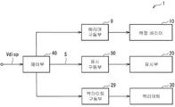
도 1은 본 발명의 한 실시예에서의 입체적 표시 장치 즉, 입체적 표시 장치(1)의 예시적 구성을 도시하는 설명도이다. 이 예에서의 입체적 표시 장치(1)는 입체적 표시 및 통상적 표시 즉, 2차원적 표시를 모두 실현할 수 있는 표시 장치이다. 이 입체적 표시 장치(1)는 제어부(40), 표시 구동부(50), 표시부(20), 백라이트 구동부(29), 백라이트(30), 배리어 구동부(9), 및 액정 배리어(10)(광 배리어 부, 광 배리어 소자)를 포함하도록 구성된다.1 is an explanatory diagram showing an exemplary configuration of a three-dimensional display device, that is, a three-
제어부(40)는 표시 구동부(50), 백라이트 구동부(29), 및 배리어 구동부(9)를 외부로부터 제공되는 영상 신호(Vdisp)에 기초하여 그 각각에 대해 제어 신호를 제공함으로써 서로 동기적으로 동작하도록 제어하는 회로이다. 구체적으로는, 제어부(40)가 표시 구동부(50)에 영상 신호(Vdisp)에 기초한 영상 신호(S)를 제공하고, 백라이트 구동부(29)에 백라이트 제어 명령을 제공하며, 배리어 구동부(9)에 배리어 제어 명령을 제공한다. 여기에서, 입체적 표시 장치(1)에 의한 입체적 표시를 위해, 영상 신호(S)는 아래에서 설명하듯이 복수의(이 예에서는 6개) 시점 영상(eyepoint picture)을 제각기 포함하는 영상 신호(SA 및 SB)에 의해 구성된다.The
표시 구동부(50)는 제어부(40)에 의해 제공되는 영상 신호(S)에 기초하여 표시부(20)를 구동하기 위한 것이다. 표시부(20)는 액정 소자들의 구동을 통해 백라이트(30)로부터 나오는 빛을 변조함으로써 표시를 수행하기 위한 것이다.The
백라이트 구동부(29)는 제어부(40)에 의해 제공되는 백라이트 제어 신호에 기초하여 백라이트(30)를 구동하기 위한 것이다. 백라이트(30)는 표시부(20)에 대해 면발광 빛을 출사하는 기능을 갖는다.The
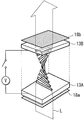
배리어 구동부(9)는 제어부(40)에 의해 제공되는 배리어 제어 명령에 기초하여 액정 배리어(10)를 구동하기 위한 것이다. 액정 배리어(10)는 복수의 개폐부(11 및 12)(아래에서 설명할)를 포함하며, 그 각각은 빛을 투과시키거나 차단한다. 이 예에서는, 배리어 구동부(9)가 표시부(20)로부터 소정의 방향을 향해 나오는 영상의 빛을 분할하는 기능을 갖는다.The
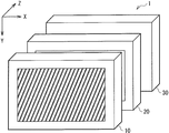
도 2a 및 2b는 제각기 입체적 표시 장치(1)의 요부의 예시적 구성을 도시하는 설명도이고, 자세하게는, 도 2a는 비스듬하게 본 입체적 표시 장치(1)의 구성을 도시하며, 도 2b는 옆에서 본 입체적 표시 장치(1)의 구성을 도시한다. 도 2a 및 2b에 도시된 바와 같이, 입체적 표시 장치(1)에서는, 표시부(20)와 액정 배리어(10)가 백라이트(30) 쪽으로부터 순서대로 배치된다. 다시 말해서, 백라이트(30)로부터 나온 빛은 관찰자에게 도달하기 전에 표시부(20)와 액정 배리어(10)를 순서대로 투과한다. 주목할 것은 표시부(20)와 액정 배리어(10)가 서로 부착되거나 부착되지 않을 수 있다는 것이다.
2A and 2B are explanatory diagrams showing an exemplary configuration of main parts of the
(표시 구동부(50) 및 표시부(20))(
도 3은 표시 구동부(50) 및 표시부(20)를 포함하는 예시적 블록도를 도시한다. 화소(Pix)는 표시부(20)에 행렬로 배열된다. 표시 구동부(50)는 타이밍 제어부(51), 게이트 드라이버(52), 및 데이터 드라이버(53)를 포함하도록 구성된다. 타이밍 제어부(51)는 게이트 드라이버(52)와 데이터 드라이버(53)의 구동 타이밍을 제어하기 위한 것이고, 제어부(40)에 의해 제공된 영상 신호(S)를 데이터 드라이버(53)에 대해 영상 신호(S1)로서 공급하기 위한 것이다. 게이트 드라이버(52)는 액정 표시 장치(45)의 선에 기초한 순차 선택을 함으로써 액정 표시 장치(45)에서 화소(Pix)(아래에서 설명할)의 선 순차 주사(line-sequential scanning)를 하기 위한 것이다. 이러한 선 순차 주사는 타이밍 제어부(51)에 의해 수행되는 타이밍 제어에 따라 수행된다. 데이터 드라이버(53)는 표시부(20)에서의 화소(Pix)의 각각에 대해 영상 신호(S1)에 기초한 화소 신호를 공급하기 위한 것이다. 구체적으로는, 데이터 드라이버(53)는 영상 신호(S1)에 기초하여 D/A (Digital/Analog) 변환을 수행하며, 그럼으로써 화소(Pix)의 각각에 공급하기 위한 아날로그 신호인 화소 신호를 발생시킨다.3 shows an exemplary block diagram including a
표시부(20)는 액정 재료를 사이에 채운 2장의 투명 기판으로 구성된 것이다. 이러한 2장의 기판은 제각기 예를 들어 유리로 이루어진다. 이러한 투명 기판들의 각각에 있어서, 액정 재료에 면하는 부분은 예를 들어 ITO(Indium Tin Oxide)로 이루어진 투명 전극으로 형성되며, 그럼으로써 액정 재료와 함께 화소(Pix)를 구성한다. 이 표시부(20)에서 그러한 액정 재료는 예를 들어 네마틱 액정을 이용한 VA(Vertical Alignment) 모드, IPS(In-Plane Switching) 모드, TN(Twisted Nematic) 모드 등으로 된 액정으로 예시된다. 아래에서는, 표시부(20)(화소(Pix))의 구성에 대해 상세하게 설명한다.The
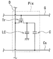
도 4a는 화소(Pix)의 예시적 회로 다이어그램을 도시하는 설명도이다. 화소(Pix)는 TFT(Thin Film Transistor) 소자(Tr), 액정 소자(LC), 및 유지 커패시터 소자(retention capacity element)(C)를 포함한다. TFT 소자(Tr)는 예를 들어 MOS-FET(Metal Oxide Semiconductor - Field Effect Transistor)으로 이루어지고, 거기에서, 게이트는 게이트 선(G)에 접속되며, 소스는 데이터 선(D)에 접속되고, 드레인은 액정 소자(LC)의 일단 및 유지 커패시터 소자(C)의 일단에 접속된다. 액정 소자(LC)에 있어서, 일단은 TFT 소자(Tr)의 드레인에 접속되고, 타단은 접지된다. 유지 커패시터 소자(C)에 있어서, 일단은 TFT 소자(Tr)의 드레인에 접속되고, 타단은 유지 커패시터 선(Cs)에 접속된다. 게이트 선(G)은 게이트 드라이버(52)에 접속되고, 데이터 선(D)은 데이터 드라이버(53)에 접속된다.4A is an explanatory diagram showing an exemplary circuit diagram of the pixel Pix. The pixel Pix includes a TFT (Tin Film Transistor) element Tr, a liquid crystal element LC, and a retention capacitor element C. The TFT element Tr is made of, for example, a MOS-FET (Metal Oxide Semiconductor-Field Effect Transistor), where the gate is connected to the gate line G, the source is connected to the data line D, The drain is connected to one end of the liquid crystal element LC and one end of the sustain capacitor element C. In the liquid crystal element LC, one end is connected to the drain of the TFT element Tr, and the other end is grounded. In the sustain capacitor element C, one end is connected to the drain of the TFT element Tr, and the other end is connected to the sustain capacitor line Cs. The gate line G is connected to the gate driver 52, and the data line D is connected to the
도 4b는 화소(Pix)를 포함하는 표시부(20)의 단면 구성을 도시하는 설명도이다. 그와 같이, 단면에서의 표시부(20)에는 액정층(203)이 구동 기판(drive substrate)(201)과 대향 기판(opposing substrate)(205) 사이에 밀봉된다. 구동 기판(201)에는 위에서 설명한 TFT 소자(Tr)를 포함하는 화소구동 회로가 형성되고, 이러한 구동 기판(201) 상에는 각각의 화소(Pix)를 위한 화소 전극(202)이 제공된다. 대향 기판(205)에는 도시되지 않은 칼라 필터 및/또는 블랙 매트릭스(black matrix)가 형성되고, 대향 기판(205)의 액정층(203) 쪽의 면에는 화소들(Pix)이 공용(shared use)하는 대향 전극(opposing electrode)(204)이 제공된다. 또한, 표시부(20)에서, 광입사측(이 예에서는 백라이트(30) 쪽)과 광출사측(이 예에서는 액정 배리어(10) 쪽)에는 편광판(206a 및 206b)이 제각기 접합되어 크로스 니콜(crossed Nichol) 또는 패럴렐 니콜(parallel Nichol)이 되게 한다.
4B is an explanatory diagram illustrating a cross-sectional structure of the
(백라이트(30))(Backlight (30))
백라이트(30)는 예를 들어 도광판의 측면 상의 LED(Light Emitting Diode) 등을 포함하도록 구성된다. 선택적으로, 백라이트(30)는 예를 들어 복수의 CCFL(Cold Cathode Fluorescent Lamp)의 배열에 의해 구성될 수 있을 것이다.
The
(액정 배리어(10))(Liquid crystal barrier 10)
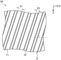
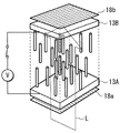
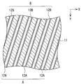
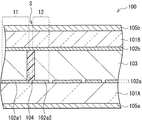
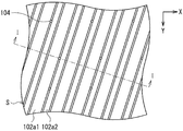
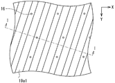
도 5는 액정 배리어(10)에서의 개폐부의 배치 구성을 도시하는 설명도이다. 도 6a는 액정 배리어(10)의 단면 구성을 도시하며, 도 6b는 투명 전극층(15a)과 스페이서(16) 사이의 배치 관계를 도시하는 XY 평면에서의 모식도이다.5 is an explanatory diagram showing the arrangement of the opening and closing portions in the
액정 배리어(10)는 이른바 시차 배리어이며, 도 5에 도시된 바와 같이, 복수의 개폐부(11)(제2 서브 영역) 및 복수의 개폐부(12)(제1 서브 영역)를 포함하고, 그 것들은 제각기 빛을 투과시키거나 차단한다. 이러한 개폐부(11 및 12)는 입체적 표시 장치(1)가 수행하려는 표시 유형, 즉, 통상적 표시(2차원적 표시) 또는 입체적 표시에 따라 상이하게 동작한다. 구체적으로는, 아래에서 설명하듯이, 개폐부(11)는 통상적 표시 동안에는 제각기 개방 상태(투과 상태)이고, 입체적 표시 동안에는 제각기 폐쇄 상태(차단 상태)이다. 아래에서 설명하듯이, 개폐부(12)는 통상적 표시 동안에는 제각기 개방 상태(투과 상태)이고, 입체적 표시 동안에는 제각기 개폐 동작을 시분할 방식으로 수행한다. 그와 같은 개폐부(11 및 12)는 제각기 교번적으로 배치되어 개폐부(11 및 12)의 어느 것이든 그룹으로서 선택적으로 구동되거나, 또는 그러한 그룹들이 예를 들어 시분할 방식으로 구동될 수 있을 것이다.The
이러한 개폐부(11 및 12)는 예를 들어 XY 평면에서의 한 방향, 여기에서는 수평 방향 X로부터 소정의 각도 θ를 이루는 방향으로 경계부(S)를 거쳐서 제각기 연장하도록 배치된다. 개폐부(11 및 12)는 제각기 값이 변하는 폭(E1 및 E2)을 가지며, 여기에서는 예를 들어 E1 > E2인 관계를 갖는다. 주목할 것은 개폐부(11 및 12)가 그러한 관계의 폭 크기로 제한되는 것이 아니며, E1 < E2 또는 E1 = E2으로 될 수도 있다는 것이다. 경계부(S)는 예를 들어 아래에서 설명할 서브 전극(15a1 및 15a2) 사이의 틈(slit)에 대응하는 부분이다. 그와 같은 개폐부(11 및 12)는 제각기 액정층 즉, 아래에서 설명할 액정층(14)을 포함하도록 구성되며, 제각기 이 액정층(14)에 대한 구동 전압에 따라 개폐된다.These
구체적으로는, 도 6a에 도시된 바와 같이, 액정 배리어(10)는 예를 들어 제각기 유리로 이루어진 투명 기판(13A 및 13B) 사이에 액정층(14)을 포함시키도록 구성된다. 이러한 투명 기판(13A 및 13B)에 있어서, 투명 기판(13A)은 광입사측에 배치되고, 투명 기판(13B)은 광출사측에 배치된다. 투명 기판(13A)의 액정층(14) 쪽 면에는 투명 전극층(15a)이 형성되고, 투명 기판(13B)의 액정층(14) 쪽 면에는 투명 전극층(15b)이 형성된다. 이러한 투명 전극층(15a 및 15b)은 제각기 예를 들어 ITO로 이루어진다. 투명 기판(13A)은 광입사측의 편광판(18a)과 접합되고, 투명 기판(13B)은 광출사측의 편광판(18b)과 접합된다. 아래에서는, 구성요소들의 각각의 구성에 대해 상세하게 설명한다.Specifically, as shown in FIG. 6A, the
액정층(14)은 예를 들어 TN 모드의 액정(TN 액정)으로 이루어진다. 이 실시예에서는, 이 액정층(14)이 예를 들어 노멀리 화이트 모드로 구동되며, 구동 전압이 인가되지 않으면 액정층(14)이 빛을 투과시키고(도 7a) 즉, 백색 표시(white display)가 수행되고, 구동 전압이 인가되면 빛을 차단하는(도 7b) 즉, 흑색 표시(black display)가 수행되는 경우가 예시된다. 더 상세하게는, 구동 전압이 인가되지 않는 백색 표시 동안에, 액정 분자의 다이렉터(director)들이 광 입사측과 출사측 사이에서 서로 직교하며, 액정층(14)의 두께 방향을 따라 회전하면서 다양한 배향으로 배열된다. 한편, 구동 전압이 인가되는 흑색 표시 동안에는, 액정 분자의 다이렉터들이 액정층(14)의 두께 방향을 따르도록 배열된다.The
투명 전극층(15a 및 15b)에 있어서, 투명 전극층(15a 및 15b)의 하나 또는 둘 모두가 제각기 개별적 전압 공급이 가능한 복수의 서브 전극(sub-electrode)으로 분할된다. 예를 들어, 투명 전극층(15a)이 복수의 서브 전극(15a1 및 15a2)으로 분할되고, 투명 전극층(15b)은 이러한 서브 전극(15a1 및 15a2)이 공용하는 전극으로서 제공된다. 서브 전극(15a1 및 15a2)에 대응하는 영역들은 제각기 개폐부(11 및 12)이며, 제각기 본 발명의 실시예에 따른 서브 영역에 상당하는 것이다. 그러한 구성은 액정층(14)의 어떤 선택적 영역에 대해서만 전압의 인가를 허용하여 개폐부(11 및 12)가 각각의 상태로 되게, 즉, 투과 상태(백색 표시) 또는 차단 상태(흑색 표시)로 전환되게 한다. 이러한 투명 전극층(15a 및 15b)에 있어서, 액정층(14) 쪽의 면에는 제각기 도시되지 않은 배향막(orientation film)이 형성된다.In the
편광판(18a 및 18b)은 제각기 액정층(14)으로 입사하는 빛과 그로부터 출사하는 빛의 편광 방향을 제어하기 위한 것이다. 액정층(14)이 예를 들어 TN 액정으로 이루어지면, 이러한 편광판(18a 및 18b)의 흡수축(absorption axis)들이 서로 직교하도록 배치된다.
The
(스페이서(16)의 배치)(Placement of spacer 16)
그러한 액정 배리어(10)에서는, 액정층(14)의 두께를 제어하기 위해 스페이서(16)가 투명 기판(13A 및 13B) 사이에 삽입되어 배치된다. 스페이서(16)는 예를 들어 포토레지스트 등과 같은 수지로 이루어지며, 예를 들어, 원주 등과 같은 기둥형상이다. 도 6a 및 6b에 도시된 바와 같이, 이 스페이서(16)는 액정 배리어(10)의 XY 평면 상의 복수의 선택적 영역, 특히 경계부(S)를 포함하지 않는 영역 즉, 개폐부(11 및 12) 사이의 경계 영역 이외의 부분에 제공된다. 이 실시예서는, 스페이서(16)가 제각기 서브 전극(15a2)의 가장자리(150e)(단부 모서리 부분)에 없는 즉, 이 예에서는 제각기 서브 전극(15a2) 상의 중앙부에 배치된다. 다시 말해서, 스페이서(16)는 제각기 서브 전극(15a1 및 15a2) 사이의 영역(경계부(S))에 가로놓여 있지 않도록 제공된다.In such a
그와 같은 스페이서(16)는 위에서 설명한 바와 같은 경계부(S)를 포함하지 않는 어떤 영역에든 제공될 수 있지만, 양호하게는, 이 실시예에서처럼, 제각기 입체적 표시 동안에 빛이 투과되는 개폐부(12)의 서브 전극(15a2) 즉, 백색 표시 영역 상에 배치된다. 그러나, 이 것은 엄격하게 제한적인 것은 아니며, 스페이서(16)는 제각기 개폐부(11)에서의 서브 전극(15a1) 상에 배치될 수 있을 것이다.
주목할 것은, 이 실시예에서는, 개폐부(11)가 폭(E1) 즉, 예를 들어 50 내지 200㎛인 서브 전극(15a1)의 폭을 가지며, 개폐부(12)는 폭(E2) 즉, 예를 들어 100 내지 500㎛인 서브 전극(15a2)의 폭을 갖고, 경계부(S)는 예를 들어 4 내지 20㎛인 폭을 갖는다. 스페이서(16)는 직경 즉, 예를 들어 10 내지 30㎛인 XY 평면 상의 원형 부분의 직경을 갖는다.Note that in this embodiment, the opening and closing
이 예에서는, 액정 배리어(10)가 노멀리 화이트 모드로 동작하는 것으로 예시되지만, 이 것은 엄격하게 제한적인 것은 아니며, 선택적으로, 액정 배리어(10)는 예를 들어 노멀리 블랙 모드(normally black mode)로 동작할 수도 있을 것이다. 그와 같은 노멀리 블랙 동작와 노멀리 화이트 동작 사이의 선택은 편광판 및 액정 배향에 의해 이루어진다.In this example, the
입체적 표시를 위해, 배리어 구동부(9)는 동일한 타이밍에서 개폐 동작을 수행하도록 개폐부(11 및 12)를 구동한다. 구체적으로는, 아래에서 상세하게 설명할 것이지만, 배리어 구동부(9)가 그룹 A에서의 복수의 개폐부(12)와 그룹 B에서의 복수의 개폐부(12)를 시분할 방식으로 교번적으로 개폐하도록 구동한다.For three-dimensional display, the
도 8은 개폐부(12)의 예시적 그룹 구성을 도시한다. 개폐부(12)는 예를 들어 2개의 그룹을 이룬다. 구체적으로는, 그룹 A는 복수의 개폐부(12A)를 포함하고, 그룹 B는 복수의 개폐부(12B)를 포함한다. 이러한 개폐부(12A 및 12B)는 교번적으로 배치되는 것이다.8 shows an exemplary group configuration of the openings and
도 9a 내지 9c는 제각기 입체적 표시와 통상적 표시(2차원적 표시)를 위한 액정 배리어(10)의 상태를 개략적으로 도시한다. 자세하게는, 도 9a는 입체적 표시를 위한 상태를 도시하고, 도 9b는 입체적 표시를 위한 다른 상태를 도시하며, 도 9c는 통상적 표시를 위한 상태를 도시한다. 액정 배리어(10)는 개폐부(11 및 12) 즉, 그룹 A에서의 개폐부(12A)와 그룹 B에서의 개폐부(12B)를 교번적으로 포함한다. 이 예에서는, 개폐부(12A 및 12B)가 제각기 표시부(20)에서의 6개의 화소(Pix)마다 제공된다. 아래의 설명에서는, 화소(Pix)가 RGB의 3개 화소를 포함하는 것으로 가정되지만, 이 것은 엄격하게 제한적인 것은 아니다. 선택적으로, 예를 들어, 화소(Pix)는 서브 픽셀(sub pixel)일 수도 있을 것이다. 주목할 것은, 액정 배리어(10)에서, 빛이 차단되는 어떤 부분이든 도면에서는 빗금이 그어져 있다는 것이다.9A to 9C schematically show the state of the
입체적 표시를 위해, 표시부(20)에서는, 영상 신호(SA 및 SB)에 기초한 영상 표시가 시분할 방식으로 수행되며, 액정 배리어(10)에서도, 개폐부(12) 즉, 개폐부(12A 및 12B)가 위에서 설명한 표시부(20)에서의 시분할적 표시와 동기적으로 개폐된다. 개폐부(12)의 그러한 개폐 동안에, 개폐부(11)는 모두 폐쇄 상태 즉, 차단 상태로 있다. 구체적으로는, 아래에서 상세하게 설명할 것이지만, 도 9a에 도시된 바와 같이, 영상 신호(SA)가 제공될 때, 액정 배리어(10)에서, 개폐부(12A)는 개방 상태로 되고, 개폐부(12B)는 폐쇄 상태로 된다. 표시부(20)는 영상 신호(SA)에 포함된 6개의 시점 영상을 이러한 개폐부(12A)에 대응하는 위치에 있는 6개의 인접 화소(Pix)에 표시한다. 마찬가지로, 도 9b에 도시된 바와 같이, 영상 신호(SB)가 제공될 때, 액정 배리어(10)에서, 개폐부(12B)는 개방 상태로 되고, 개폐부(12A)는 폐쇄 상태로 된다. 표시부(20)는 영상 신호(SB)에 포함된 6개의 시점 영상을 이러한 개폐부(12B)에 대응하는 위치에 있는 6개의 인접 화소(Pix)에 표시한다.For three-dimensional display, in the
한편, 통상적 표시(2차원적 표시)를 위해, 도 9c에 도시된 바와 같이, 표시부(20)는 영상 신호(S)에 기초하여 표시를 생성하고, 액정 배리어(10)에서, 개폐부(11 및 12) 즉, 개폐부(12A 및 12B)는 개방 상태 즉, 투과 상태로 있다.
Meanwhile, for normal display (two-dimensional display), as shown in FIG. 9C, the
(동작 및 작용)(Operation and Action)
다음으로, 이 실시예에서의 입체적 표시 장치(1)의 동작 및 작용에 대해 설명한다.
Next, the operation and operation of the three-
(전체 동작의 개요)(Overview of overall operation)
제어부(40)는 표시 구동부(50), 백라이트 구동부(29), 및 배리어 구동부(9)를 외부로부터 제공되는 영상 신호(Vdisp)에 기초하여 그 것들의 각각에 대해 제어 신호를 제공함으로써 서로 동기적으로 동작하도록 제어한다. 백라이트 구동부(29)는 제어부(40)에 의해 제공되는 백라이트 제어 신호에 기초하여 백라이트(30)를 구동한다. 백라이트(30)는 면발광 빛을 표시부(20)에 출사한다. 표시 구동부(50)는 제어부(40)에 의해 제공되는 영상 신호(S)에 기초하여 표시부(20)를 구동한다. 표시부(20)는 백라이트(30)로부터 나오는 빛을 변조함으로써 표시를 수행한다. 배리어 구동부(9)는 제어부(40)에 의해 제공되는 배리어 제어 명령에 기초하여 액정 배리어(10)를 구동한다. 액정 배리어(10)는 백라이트(30)로부터 나오는 빛을 그 빛이 표시부(20)를 투과한 후 투과시키거나 차단한다.
The
(입체적 표시의 상세 동작)(Detailed operation of three-dimensional display)
다음에서는 몇몇 도면을 참조하여 입체적 표시의 상세 동작에 대해 설명한다.Next, a detailed operation of the stereoscopic display will be described with reference to some drawings.
도 10a 및 10b는 제각기 표시부(20)의 예시적 동작 및 액정 배리어(10)의 예시적 동작을 도시하며, 자세하게는, 도 10a는 영상 신호(SA)가 제공되는 경우를 도시하고, 도 10b는 영상 신호(SB)가 제공되는 경우를 도시한다.10A and 10B illustrate an exemplary operation of the
도 10a에 도시된 바와 같이, 영상 신호(SA)가 제공될 때, 표시 구동부(50)는 6개의 화소의 화소 정보(P1 내지 P6)를 표시부(20)에서의 6개의 인접 화소(Pix)에 표시한다. 이러한 화소 정보(P1 내지 P6)는 제각기 영상 신호(SA)에 포함된 6개의 시점 영상에 대응하는 것이다. 이러한 화소 정보(P1 내지 P6)를 표시하는 6개의 화소는 개폐부(12A)의 근처에서 서로 인접해 있는 화소인 것으로 한다. 한편, 액정 배리어(10)에서는, 위에서 설명한 바와 같이, 개폐부(12A)가 모두 개방 상태(투과 상태)로 있도록 제어되고, 개폐부(12B)는 모두 폐쇄 상태로 있도록 제어된다(개폐부(11)는 모두 폐쇄 상태로 있도록 제어된다). 그와 같이, 표시부(20)에서의 화소(Pix)의 각각으로부터 나오는 빛은 개폐부(12A)에 의한 발광 각도에서 제한된다. 다시 말해서, 공간 분할적 방식으로 표시부(20)에 표시된 6개의 시점 영상이 개폐부(12)에 의해 분리된다. 그와 같이 분리된 시점 영상에 있어서, 예를 들어 화소 정보(P3)에 기초한 영상의 빛은 관찰자의 좌안에 의해 보여지고, 화소 정보(P4)에 기초한 영상의 빛은 관찰자의 우안에 의해 보여져서 영상이 관찰자에 의해 3차원적으로 인식되게 한다.As shown in FIG. 10A, when the image signal SA is provided, the
이 것은 영상 신호(SB)가 제공되고, 도 10b에 도시된 바와 같이, 표시 구동부(50)가 6개의 화소의 화소 정보(P1 내지 P6)를 표시부(20)에서의 6개의 인접 화소(Pix)에 표시하는 경우에도 적용할 수 있다. 이러한 화소 정보(P1 내지 P6)는 제각기 영상 신호(SB)에 포함된 6개의 시점 영상에 대응하는 것이다. 이러한 화소 정보(P1 내지 P6)를 표시하는 6개의 화소는 개폐부(12B)의 근처에서 서로 인접해 있는 화소인 것으로 한다. 한편, 액정 배리어(10)에서는, 위에서 설명한 바와 같이, 개폐부(12B)가 모두 개방 상태(투과 상태)로 있도록 제어되고, 개폐부(12A)는 모두 폐쇄 상태로 있도록 제어된다(개폐부(11)는 모두 폐쇄 상태로 있도록 제어된다). 그와 같이, 표시부(20)에서의 화소(Pix)의 각각으로부터 나오는 빛은 개폐부(12B)에 의한 발광 각도에서 제한된다. 다시 말해서, 공간 분할적 방식으로 표시부(20)에 표시된 6개의 시점 영상이 개폐부(12B)에 의해 분리된다. 그와 같이 분리된 시점 영상에 있어서, 예를 들어 화소 정보(P3)에 기초한 영상의 빛은 관찰자의 좌안에 의해 보여지고, 화소 정보(P4)에 기초한 영상의 빛은 관찰자의 우안에 의해 보여져서 영상이 관찰자에 의해 3차원적으로 인식되게 한다.This is provided with an image signal SB, and as shown in FIG. 10B, the
그와 같이, 관찰자에 있어서, 그 또는 그녀의 좌우의 눈은 그러한 P1 내지 P6의 어느 것이든 상이한 화소 정보들을 보게 되어 관찰자가 영상을 3차원적으로 인식하게 한다. 또한, 개폐부(12A 및 12B)를 시분할 방식으로 교번적으로 개폐하는 것에 의한 영상 표시에 따라, 관찰자는 정렬되지 않은 상이한 위치에 표시된 영상들을 균일하게 보게 된다. 그와 같이, 입체적 표시 장치(1)는 복수의 개폐부(12)를 그룹화 하지 않고 일괄적으로 구동하는 경우보다 2배 높은 해상도를 달성하게 한다. 다시 말해서, 입체적 표시 장치(1)는 2차원적 표시의 해상도의 1/3(= 1/6 × 2)의 해상도이어도 좋다.As such, for the observer, his or her left and right eyes see different pixel information in either of those P1 to P6, allowing the observer to perceive the image in three dimensions. In addition, according to the image display by alternately opening and closing the
그와 같이 개폐부(11 및 12)를 포함하는 액정 배리어(10)는 투명 기판(13A 및 13B) 사이에 밀봉된 액정층(14)을 포함하고, 개폐부(11 및 12)의 각각에 대응하는 각각의 영역에 대한 개별적 전압 인가에 의해 투광과 차광 사이의 상태가 전환된다. 따라서, 액정층(14)에 대한 전압 인가를 위한 투명 전극층(15a 및 15b)에 있어서, 투명 전극층(15a)은 복수의 서브 전극(15a1 및 15a2)으로 분할된다. 또한, 그러한 구성에서는, 액정층(14)의 두께를 제어하기 위해 이용하는 스페이서(16)가 복수의 소정의 영역에 배치된다. 아래에서는, 스페이서(16)의 설치의 효과를 비교예에 의해 설명한다.
As such, the
(비교예)(Comparative Example)
도 11a 및 11b는 비교예에서의 액정 배리어(액정 배리어(100))의 예시적 단면 구성 및 스페이서의 배치 구성을 제각기 도시하는 설명도이다. 실시예와 마찬가지로, 액정 배리어(100)는 투명 기판(101A 및 101B) 사이에 밀봉된 액정층(103)을 포함하고, 액정층(103)에 대한 전압 인가를 위한 투명 전극층(102a 및 102b)이 제공된다. 투명 기판(101A)은 광입사측의 편광판(105a)과 접합되고, 투명 기판(101B)은 광출사측의 편광판(105b)과 접합된다. 투명 전극층(102a 및 102b)에 있어서, 투명 전극층(102a)은 복수의 투명 전극(120a1 및 102a2)으로 분할되고, 투명 전극(102a1 및 102a2)에 대응하는 영역들은 제각기 개폐부이다. 그러한 구성에서는, 액정층(103)의 두께를 제어하기 위한 목적으로 스페이서(104)가 투명 기판(101A 및 101B) 사이에 삽입되어 제공된다. 주목할 것은, 이 비교예의 액정 배리어(100)에서는, 스페이서(104)가 제각기 투명 전극(102a1 및 102a2) 사이의 영역에 가로놓여 있도록 배치, 즉, 경계부(S)에 배치된다는 것이다.11A and 11B are explanatory diagrams respectively showing an exemplary cross-sectional configuration of the liquid crystal barrier (liquid crystal barrier 100) and the arrangement of the spacers in the comparative example. Similar to the embodiment, the
여기에서의 문제는, 스페이서(104)가 그와 같이 경계부(S)에 배치되어 있으면, 투명 전극(102a1 및 102a2)의 가장자리의 영향으로 인해, 특히 프린지 필드의 발생으로 인해 액정층(103)의 배향이 크게 흐트러지기 쉽다는 것이다. 액정층(103)이 예를 들어 노멀리 화이트 모드로 구동되면, 흑색 표시를 위한 투명 전극(102a2)(또는 투명 전극(102a1))에 대응하는 어떤 영역에든 전압이 인가된다. 이 경우에, 스페이서(104)의 각각의 근처의 영역은 액정 배향이 요구된 방향에 있지 않기 때문에 부분적으로 빛을 너무 많이 투과시킨다. 결과적으로, 스페이서(104)의 각각의 근처에서 너무 많은 광 누출이 일어나서 그 부분이 잔여 에리어보다 더 희끄무리하게 보이게 한다.The problem here is that if the
한편, 실시예에서는, 스페이서(16)가 경계부(S)를 포함하지 않는 영역 즉, 경계 영역 이외의 부분에 배치된다. 다시 말해서, 스페이서(16)는 제각기 서브 전극(15a2) 상의 액정 배향이 안정적인 영역에 배치되며, 그럼으로써 비교예에서 스페이서의 배치에 의해 유발되는 투과율의 변화를 방지한다.
On the other hand, in the embodiment, the
(예)(Yes)
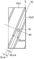
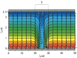
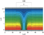
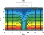
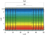
여기에서는, 2가지 경우 즉, 스페이서(104)가 비교예에서와 같이 경계부(S)에 배치된 한 경우 및, 스페이서(16)가 실시예 즉, 예 1에서와 같이 경계 영역 이외의 부분에(서브 전극(15a2) 상에) 배치된 다른 경우에, 액정층에서의 전기장 분포와 배향 상태에 대한 시뮬레이션이 수행되었다. 이 시뮬레이션을 위해, 비교예에서는, 스페이서(104)가 제각기 도 12a에 도시된 바와 같이 경계부(S) 상에 직접 배치되었고, 경계부(S)는 8㎛의 폭을 갖도록 설정되었으며, 스페이서(104)는 20㎛의 직경을 갖도록 설정되었다. 한편, 예 1에서는, 도 12b에 도시된 바와 같이, 스페이서(16)가 제각기 서브 전극(15a2) 상의 중앙부에 배치되었고, 경계(S)는 8㎛의 폭을 갖도록 설정되었으며, 스페이서(16)는 20㎛의 직경을 갖도록 설정되었고, 서브 전극(15a2)은 50㎛의 폭(E2)을 갖도록 설정되었다. 또한, 비교예와 예 1 모두에서, 액정층은 3.5㎛의 두께(스페이서의 높이)를 갖도록 설정되었다.Here, in two cases, namely, the
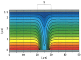
도 14a는 비교예에서의 그와 같은 계산 결과의 등전위 분포를 도시하고, 도 14b는 거기에서의 액정 배향의 상태를 도시한다. 도 15a는 예 1에서의 등전위 분포를 도시하고, 도 15b는 거기에서의 액정 배향의 상태를 도시한다. 또한, 도 13a 및 13b는 제각기 경계부(S)의 근처에서의 등전위 분포 및 거기에서의 액정 배향의 상태를 도시한다. 여기에서, 도 13a 및 13b는 제각기 도 12a의 선 X1에 따른 경계부(S) 근처에서의 단면에 대응하며, 도 14a 및 14b는 제각기 도 12a의 선 X2에 따른 경계부(S) 근처에서의 단면에 대응한다. 도 15a 및 15b는 제각기 도 12b의 선 X3에 따른 개폐부(12) 즉, 서브 전극(15a2)에 대응하는 영역의 단면에 대응한다. 색상 변화는 전위 변화를 나타내며, 블루, 그린, 옐로우, 오렌지, 레드의 순서로 전위의 점진적인 증가를 도시하고, 즉, 블루 부분은 최저 전위(이 예에서는0V)이며, 레드 부분은 최고 전위(이 예에서는7V)이다.FIG. 14A shows the equipotential distribution of such a calculation result in the comparative example, and FIG. 14B shows the state of liquid crystal alignment there. FIG. 15A shows an equipotential distribution in Example 1, and FIG. 15B shows a state of liquid crystal alignment therein. 13A and 13B show the equipotential distribution in the vicinity of the boundary S, respectively, and the state of the liquid crystal alignment therein. 13A and 13B respectively correspond to a cross section near the boundary S along the line X1 in FIG. 12A, and FIGS. 14A and 14B respectively show a cross section near the boundary S along the line X2 in FIG. 12A. Corresponds. 15A and 15B respectively correspond to a cross section of the opening / closing
도 13a 및 13b에 도시된 바와 같이, 경계부(S)에 대응하는 영역에서는, 전극의 가장자리의 영향으로 인해 프린지 필드가 발생된다. 그래서, 액정 분자가 충분히 세워지지 못하기 때문에 액정 배향이 흐트러지는 것으로 알려져 있다. 그와 같은 비교예에서와 같이, 스페이서(104)가 경계부(S)에 배치되면, 전기장 분포 및 액정 배향은 제각기 도 14a 및 14b에 도시된 것과 같이 보인다. 그러므로, 경계부(S)에 대응하는 영역 즉, 도 12a의 선 Y1에 따른 단면에서는, 도 13a의 전기장 분포 및 도 14a의 전기장 분포가 모두 존재한다. 이 것은, 액정 배향에 있어서도, 도 13b의 배향 상태 및 도 14b의 배향 상태가 모두 스페이서(104)의 주변에 존재함을 의미한다. 결과적으로, 스페이서(104)의 근처에서, 액정 배향이 더 불안정해지고, 그럼으로써 경계부(S) 및 스페이서(104)의 근처의 영역에서의 광 누출을 유발하기 쉽다. 주목할 것은, 도 14a 및 14b에서, 인용부호 104D는 스페이서(104)가 배치된 영역을 지칭한다.As shown in FIGS. 13A and 13B, in the region corresponding to the boundary S, a fringe field is generated due to the influence of the edge of the electrode. Therefore, it is known that the liquid crystal alignment is disturbed because the liquid crystal molecules are not sufficiently erected. As in such a comparative example, when the
한편, 예 1에서는, 도 15a 및 15b에 도시된 바와 같이, 스페이서(16)가 전기장 분포가 평탄한 서브 전극(15a2) 상에 배치되어 있기 때문에 액정 배향이 흐트러지지 않는다. 그럼으로써, 전기장 분포는 선 X3에 따른 단면 및 선 Y2에 따른 단면에서 대칭으로 되므로 액정 배향이 안정해진다. 주목할 것은, 도 15a 및 15b에서, 인용부호 16D는 스페이서(16)가 배치된 영역을 지칭한다. 그와 같이, 스페이서(16)가 개폐부(11 및 12) 사이의 비경계 부분 영역에 배치된 실시예에서는, 스페이서의 설치로 인해 액정 배향이 흐트러지지 않으며, 그럼으로써 스페이서의 설치에 의해 유발되는 투과율의 변화를 양호하게 방지한다.On the other hand, in Example 1, as shown in Figs. 15A and 15B, the alignment of the liquid crystal is not disturbed because the
서브 전극(15a2) 상에 배치된 스페이서(16)에 따라 즉, 입체적 표시 동안에 백색으로 표시될 개폐부(12)에 배치된 스페이서(16)에 따라, 아래와 같은 효과가 생긴다. 스페이서(16)가 그 근방의 액정 배향에 영향을 미치므로, 스페이서(16) 주변의 에리어에서 광 누출이 발생하며, 그래서 산출되는 표시가 충분한 흑색이 아니다. 그와 같이, 흑색 표시(차단 영역)를 위해 이용되는 개폐부(11)가 아닌(서브 전극(15a1) 상이 아닌) 백색 표시(투과 영역)로서 이용되는 개폐부(12)(서브 전극(15a2) 상)에 스페이서(16)를 제공함으로써, 흑색 표시 부분에서의 광 누출이 성공적으로 방지된다.According to the
이 경우에, 스페이서(16)는 제각기 서브 전극(15a2)의 가장자리(150e)에 없는 것이 양호하고, 더 양호하게는, 그 것들이 제각기 서브 전극(15a2) 상의 중앙부에 배치된다. 이 것은 전기장 분포가 더 평탄한 영역에 스페이서(16)가 배치되고, 그럼으로써 스페이서의 설치에 의해 액정 배향이 흐트러지는 것을 더 잘 방지한다는 것을 의미한다.In this case, the
위에서 설명한 바와 같이, 실시예에서는, 표시부(20)가 공간 분할적 방식으로 복수의 시점 영상을 표시하고, 그렇게 표시된 영상들이 액정 배리어(10)의 복수의 개폐부(11 및 12)에 의해 투과 또는 차단된다. 그와 같이, 관찰자에 있어서, 그 또는 그녀의 좌우의 눈은 상이한 투시 이미지(perspective image)들을 인식하므로 입체적 표시가 생성된다. 액정 배리어(10)에서는, 경계부(S)를 포함하지 않는 영역(경계 영역 이외의 부분; 이 예에서는 서브 전극(15a2) 상)에 스페이서(16)를 제공함으로써, 스페이서(16)는 전기장 분포가 평탄한 어떤 영역에든 즉, 액정 배향이 안정한 영역에 배치될 것이고, 그럼으로써 스페이서의 설치로 인한 투과율의 어떤 변화든 방지할 수 있다. 그와 같이, 광 얼룩이 발생할 어떤 가능성도 방지할 수 있는 액정 배리어(10)가 실현된다.As described above, in the embodiment, the
주목할 것은, 위에서 설명한 실시예에서는, 스페이서(16)가 개폐부(12)에 배치되는 경우가 예시되었다는 것이다. 그러나, 스페이서(16)는 그 것이 경계부(S)를 포함하지 않는 영역에 배치되기만 하면 기능을 잘 할 수 있을 것이며, 즉, 개폐부(11)에 배치될 수도 있을 것이다. 그러나, 위에서 설명한 이유로 인해, 스페이서(16)는 흑색 표시의 개폐부(11)가 아닌 백색 표시의 개폐부(12)에 배치되는 것이 양호하다.
Note that in the above-described embodiment, the case where the
(변형례)(Variation)
다음으로, 위에서 설명한 실시예의 변형례에서의 액정 배리어에 대해 설명한다. 여기에서, 위에서 설명한 실시예에서의 구성요소와 동일한 어떤 구성요소든 동일한 인용부호가 제공되고, 적절하다면 다시 설명하지 않는다.
Next, the liquid crystal barrier in the modification of the above-described embodiment will be described. Here, the same reference numerals are provided for any components that are the same as the components in the above-described embodiment, and will not be described again if appropriate.
(구성)(Configuration)
도 16a는 변형례에서의 액정 배리어 즉, 액정 배리어(10a)의 단면 구성을 도시하고, 도 16b는 투명 전극층과 스페이서 사이의 배치 관계를 도시하는 XY 평면에서의 개략적 평면도이다. 액정 배리어(10a)는 위에서 설명한 실시예에서의 그 것들과 마찬가지로 백라이트(30) 및 표시부(20)를 포함하는 입체적 표시 장치에서 이용하는 시차 배리어이다. 액정 배리어(10a)는 액정층(14)을 포함하도록 구성되며, 입체적 표시를 위해, 광 차단 영역과 광 투과 영역이 교번적으로 형성되도록 구동된다.FIG. 16A shows a cross-sectional configuration of a liquid crystal barrier, that is, a
이 변형례의 액정 배리어(10a)에서는, 복수의 개폐부(11) 즉, 제3 서브 영역과 복수의 투광부(22) 즉, 제4 서브 영역이 교번적으로 배치된다. 개폐부(11)는 광 투과와 차단 사이에서 상태가 전환되도록 허용되며, 투광부(22)는 통상적으로 구동 전압에 무관하게 빛을 투과시킨다. 다시 말해서, 액정 배리어(10a)에서는, 위에서 설명한 실시예와 마찬가지로, 개폐부(11)는 통상적 표시 동안에 개방 상태로 되도록 제어되고, 입체적 표시 동안에 폐쇄 상태로 되도록 제어된다. 한편, 투광부(22)는 표시 유형 즉, 통상적 표시 또는 입체적 표시에 무관하게 개방 상태로 되도록 제어된다. 아래에서는, 그러한 액정 배리어(10a)의 상세한 구성을 설명한다.In the
위에서 설명한 실시예에서의 액정 배리어(10)와 마찬가지로, 액정 배리어(10a)는 투명 기판(13A 및 13B) 사이의 액정층(14)을 포함한다. 투명 기판(13A)의 액정층(14) 쪽 면에는 투명 전극층(19a)이 형성되며, 투명 기판(13B)의 액정층(14) 쪽 면에는 투명 전극층(15b)이 형성된다. 투명 기판(13A)은 광입사측의 편광판(18a)과 접합되며, 투명 기판(13B)은 광출사측의 편광판(18b)과 접합된다.Similar to the
적어도 투명 전극층(19a 또는 15b)(이 예에서는 투명 전극층(19a))은 위에서 설명한 실시예와 마찬가지로 복수의 서브 전극(19a1)으로 분할된다. 주목할 것은, 이 변형례에서는, 이러한 서브 전극(19a1)이 개폐부(11)에만 배치되고, 투광부(22)에는 배치되지 않는다는 것이다. 다시 말해서, 투광부(22)는 투명 기판의 적어도 한 쪽에서 아무런 전극도 포함하지 않는 전극 비형성 영역이다. 투명 기판(13B) 쪽의 투명 전극층(15b)에 있어서, 위에서 설명한 실시예와 마찬가지로, 그 것은 복수의 서브 전극(19a1)이 공용하도록 형성된 이른바 솔리드 전극(solid electrode)이다. 그러한 구성에 따라, 개폐부(11)는 구동 전압의 인가에 의해 광 차단과 투과 사이에서 상태가 전환되도록 허용된다. 한편, 예를 들어 액정층(14)이 노멀리 화이트 모드로 구동되면 투광부(22)는 상시 백색 표시의 광 투과 영역으로서의 기능을 한다.At least the
개폐부(11)는 XY 평면에서의 한 방향 예를 들어, 수평 방향 X로부터 소정의 각도 θ를 이루는 방향으로 투광부(22)에 대응하는 소정의 간격으로 연장하도록 배치된다. 여기에서, 개폐부(11)와 투광부(22)는 제각기 상이한 폭을 갖거나 또는 갖지 않을 수 있을 것이다.The opening / closing
그러한 구성에서, 이 변형례에서도, 액정층(14)의 두께를 제어하기 위해 복수의 스페이서(16)가 투명 기판(13A 및 13B) 사이에 삽입되어 배치된다. 스페이서(16)는 액정 배리어(10)의 XY 평면 상에서의 복수의 선택적 영역, 특히 경계부(S1)를 포함하지 않는 영역 즉, 개폐부(11)와 투광부(22) 사이의 경계 영역 이외의 부분에 제공된다. 다시 말해서, 스페이서(16)는 서브 전극(19a1)의 가장자리 부분이 아닌 곳에 제공되며, 즉, 서브 전극(19a1)의 가장자리 부분에 없다. 구체적으로는, 스페이서(16)는 제각기 투광부(22)의 중앙부에 제공된다. 스페이서(16)는 경계부(S1)를 포함하지 않는 영역 즉, 개폐부(11)와 투광부(22) 중 투광부(22)에 제공되는 것이 양호하다. 이 것은, 노멀리 화이트 모드에서는, 스페이서(16) 주변의 에리어가 위 실시예에서 설명한 바와 같이 충분한 흑색으로 표시되지 않고, 그래서 스페이서(16)는 흑색 표시 영역이 아닌 백색 표시 영역에 배치되는 것이 양호하기 때문이다.
In such a configuration, even in this modification, a plurality of
(작용)(Action)
이 변형례에서는, 백라이트(30)로부터 나오는 빛을 그 빛이 표시부(20)를 투과한 후 액정 배리어(10)에서의 개폐부(11)에 의해 차단하고, 그 후 그 빛을 투광부(22)를 통해 투과시키는 것에 의한 시점 영상들의 분리의 결과로서 입체적 표시가 생성된다. 이 변형례에서는, 모든 투광부(22)가 상시 투광부로서의 기능을 하도록 되어 있으므로, 위에서 설명한 실시예처럼 그룹마다 시분할 방식으로 표시가 수행되는 것은 아니지만, 투광부(22)에 전압을 공급할 필요는 없다. 따라서, 구성이 단순해지도록 전극 배선이 감소되는 것이 양호하다. 여기에서, 개폐부(11)를 개방 상태로 함으로써 2차원적 표시가 실현된다.In this modification, light emitted from the
위와 같은 액정 배리어(10a)는 투명 기판(13A 및 13B) 사이에 복수의 스페이서(16)를 포함시킨다. 이 변형례에서도, 경계부(S1)를 포함하지 않는 영역에 이러한 스페이서(16)가 배치된다. 개폐부(11)에는 제각기 서브 전극(19a1)이 제공되므로, 경계부(S1)에서는, 서브 전극(19a1)의 가장자리의 영향으로 인해 프린지 필드가 발생되고, 그럼으로써 액정 배향이 흐트러진다. 이 변형례에서는, 액정 배향이 흐트러지는 영역이 아닌 곳에 스페이서(16)를 제공함으로써, 스페이서의 설치에 의해 유발되는 액정 배향의 혼란의 가능성이 방지될 수 있을 것이다. 또한, 위에서 설명한 바와 같이 상시 백색 표시의 투광부(22)에 스페이서(16)를 제공함으로써, 스페이서(16) 자체를 통해 빛을 투과시킴으로써 유발될 가능성이 있는 어떤 투과율 변화든 방지될 수 있을 것이다. 그와 같이, 위에서 설명한 실시예에서와 유사한 효과가 얻어질 수 있다.
The
(예)(Yes)
여기에서는, 스페이서(16)가 변형예, 즉 예 2에서와 같이 경계 영역 이외의 부분(투광부(22))에 배치된 경우에, 액정층에서의 전기장 분포와 배향 상태에 대한 시뮬레이션이 수행되었다. 이 시뮬레이션을 위해, 스페이서(16)가 제각기 투광부(22)에 대응하는 영역의 중앙부 즉, 서브 전극(19a1) 사이의 영역에 배치되었다. 스페이서(16)는 20㎛의 직경을 갖도록 설정되었고, 투광부(22)는 50㎛의 폭을 갖도록 설정되었으며, 액정층은 3.5㎛의 두께(스페이서의 높이) 갖도록 설정되었다.Here, in the case where the
도 18a는 예 2에서의 그와 같은 계산 결과의 등전위 분포를 도시하고, 도 18b는 거기에서의 액정 배향의 상태를 도시한다. 여기에서, 도 18a 및 18b는 제각기 도 17의 선 X4에 따른 투광부(22)의 단면에 대응한다. 전위와 색상 사이의 관계는 위에서 설명한 예 1에서와 유사하다. 그러나, 투광부(22)는 투명 기판(13A) 쪽에서 아무런 전극도 갖지 않으므로, 액정층(14)은 예를 들어 그 전체에서 0V이다. 그와 같은 예 2에서는, 제각기 상시 백색 표시 영역인 투광부(22)에 스페이서(16)가 배치되므로, 제각기 흑색 표시 영역인 개폐부(11)에서 액정 배향이 흐트러지지 않는다.FIG. 18A shows an equipotential distribution of such a calculation result in Example 2, and FIG. 18B shows the state of liquid crystal alignment there. 18A and 18B respectively correspond to the cross section of the
주목할 것은, 위에서 설명한 변형례에서는, 스페이서(16)가 투광부(22)에 배치되는 경우가 예시되었다는 것이다. 그러나, 투광부(22)는 엄격하게 제한적인 것이 아니며, 스페이서(16)는 그 것이 경계부(S1)를 포함하지 않는 영역에 배치되기만 하면, 즉, 서브 전극(19a1)의 가장자리 부분에 없으면 기능을 잘 할 수 있다. 선택적으로, 스페이서(16)는 개폐부(11)에 배치될 수도 있을 것이다. 그러나, 위에서 설명한 바와 같이, 스페이서(16)는 흑색 표시의 개폐부(11)가 아닌 백색 표시의 개폐부(12) 즉, 이 예에서는 투광부(22)에 배치되는 것이 양호하다.Note that, in the modification described above, the case where the
그와 같이, 실시예 및 변형례에 의해 본 발명을 상세하게 설명하였지만, 앞서의 설명은 모두 예시적인 것이며 제한적인 것이 아닌 양태들에 관한 것이다. 수많은 다른 변형 및 변화가 이루어질 수 있음을 알아야 한다. 예를 들어, 위에서 설명한 실시예 등에서는, 표시부(20) 및 액정 배리어(10)가 백라이트(30) 쪽으로부터 순서대로 배치된다. 선택적으로, 표시부(20)와 액정 배리어(10) 사이의 배치 관계는 역전될 수도 있을 것이다. 다시 말해서, 백라이트(30)와 표시부(20) 사이에 액정 배리어(10)가 제공될 수도 있을 것이다. 그러한 구성이라면, 위에서 설명한 바와 같이 표시부(20) 상의 영상 표시와 동기적으로 액정 배리어(10)의 개폐부에서 개폐 동작함으로써 입체적 표시가 실현된다.As such, while the invention has been described in detail by way of examples and modifications, the foregoing description is in all aspects illustrative and not restrictive. It should be appreciated that many other variations and changes can be made. For example, in the above-described embodiment, the
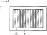
또한, 위에서 설명한 실시예 등에서는, 액정 배리어에서의 복수의 개폐부가 XY 평면 상의 대각선 방향으로 연장하는 경우가 예시된다. 개폐부의 설치는 그러한 대각선 방향으로 제한되는 것이 아니다. 도 19에 도시된 바와 같이, 예를 들어, 복수의 개폐부(31 및 32)는 광 투과 또는 차단을 위해 Y 방향을 따라 교번적으로 제공될 수 있을 것이다.In the above-described embodiments, a case where the plurality of openings and closing portions in the liquid crystal barrier extend in the diagonal direction on the XY plane is exemplified. Installation of the opening and closing portion is not limited to such a diagonal direction. As shown in FIG. 19, for example, the plurality of openings and closing
또한, 위에서 설명한 실시예에서도, 입체적 표시를 위해, 액정 배리어(10)에서의 복수의 개폐부(11 및 12)에서, 개폐부(11)는 폐쇄 상태로 되게 구동되며, 개폐부(12)는 영상 신호에 기초하여 개방 상태로 되게 구동된다. 선택적으로, 그러한 구동이 역으로 수행될 수도 있을 것이며, 즉, 개폐부(12)는 폐쇄 상태로 되고, 개폐부(11)는 영상 신호에 기초하여 개방 상태로 된다.Further, even in the above-described embodiment, for the three-dimensional display, in the plurality of openings and closing
또한, 위에서 설명한 실시예에서는, 고해상도를 얻기 위해, 개폐부(11 및 12) 중에서, 개폐부(12)는 2개의 그룹 A 및 B로 분할되며, 이러한 그룹 A 및 B는 시분할 방식으로 구동된다. 그러나, 본 발명에서는, 그와 같은 시분할 방식의 영상 표시가 반드시 예상되는 것은 아니다. 다시 말해서, 예를 들어, 액정 배리어(10)에서의 개폐부(11) 모두가 폐쇄 상태로 되게 구동되며, 개폐부(12) 모두가 개방 상태로 되게 구동되고, 그럼으로써 시점 영상들을 분리할 수도 있을 것이다. 선택적으로, 개폐부(12)는 3개 이상의 그룹으로 분할되고, 이러한 3개 이상의 그룹이 순차적으로 구동될 수도 있을 것이다.Further, in the embodiment described above, in order to obtain high resolution, among the
또한, 위에서 설명한 실시예 등에서, 영상 신호(SA 및 SB)는 제각기 6개의 시점 영상을 포함하는 것으로 한다. 이것은 엄격한 것이 아니라 단지 선택적인 것이며, 영상 신호들은 제각기 5개 이하의 시점 영상 또는 7개 이상의 시점 영상을 포함할 수도 있을 것이다. 예를 들어 영상 신호가 5개의 시점 영상을 포함하면, 개폐부(12)는 제각기 표시부(20)에서의 모든 5개의 화소(Pix)마다 제공될 수도 있을 것이다. 여기에서, 시점 영상들은 그 표시를 위한 화소만큼 많이 제공될 필요가 있는 것은 아니다. 다시 말해서, 예를 들어, 복수의 인접 화소로 표시할 화소 정보들이 반드시 상이한 시점들로부터 보는 것일 필요는 없을 것이며, 일부는 동일한 시점으로부터 보는 것일 수도 있을 것이다.In the above-described embodiments, the image signals SA and SB each include six viewpoint images. This is not rigorous but merely optional, and the image signals may include up to five viewpoint images or seven or more viewpoint images, respectively. For example, if the image signal includes five viewpoint images, the opening and
본 발명은 2010년 8월 20일에 일본 특허청에 제출되고, 그 전체 내용이 여기에 참고로 통합되는 일본 우선권 특허출원 2010-185368호에 개시된 것과 관련된 요지를 포함한다.The present invention includes the subject matter related to that disclosed in Japanese Patent Office on August 20, 2010, and disclosed in Japanese Priority Patent Application 2010-185368, the entire contents of which are incorporated herein by reference.
Claims (12)
한 쌍의 기판 사이에 밀봉되어, 제각기 빛이 투과하게 하거나 차단되게 하는 복수의 서브 영역을 포함하는 액정층, 및
상기 한 쌍의 기판 사이에서 상기 서브 영역 사이의 경계 영역 이외의 영역에 제각기 제공되어 있는 스페이서들을 포함하는, 광 배리어 소자.As an optical barrier element,
A liquid crystal layer sealed between the pair of substrates, the liquid crystal layer comprising a plurality of sub-regions, each allowing light to pass through or blocked;
And spacers that are respectively provided in regions other than the boundary region between the sub-regions between the pair of substrates.
상기 액정층에 전압이 공급되게 하는 한 쌍의 전극을 포함하고,
상기 한 쌍의 전극 중 하나 또는 둘 모두는 상기 서브 영역마다 서브 전극을 제각기 포함하고,
상기 스페이서들은 복수의 서브 전극 중에서 선택된 서브 전극 상에 제공되어 있는, 광 배리어 소자.The method of claim 1,
A pair of electrodes for supplying a voltage to the liquid crystal layer,
One or both of the pair of electrodes each include a sub-electrode for each of the sub-regions,
And the spacers are provided on a sub electrode selected from among a plurality of sub electrodes.
상기 서브 영역들은 빛이 투과되게 하는 제1 서브 영역 및 빛이 차단되게 하는 제2 서브 영역을 포함하고,
상기 스페이서는 상기 제1 서브 영역 내의 상기 서브 전극 상에 제공되어 있는, 광 배리어 소자.The method of claim 2,
The sub-regions include a first sub-region through which light is transmitted and a second sub-region through which light is blocked,
And the spacer is provided on the sub-electrode in the first sub-region.
상기 스페이서는 상기 서브 전극의 가장자리에 없는, 광 배리어 소자.The method of claim 3,
And the spacer is not at the edge of the sub-electrode.
상기 스페이서는 상기 서브 전극의 상기 가장자리로부터 떨어진 중앙에 제공되어 있는, 광 배리어 소자.The method of claim 4, wherein
And the spacer is provided at the center away from the edge of the sub-electrode.
상기 액정층에 전압이 공급되게 하는 한 쌍의 전극을 포함하고,
상기 한 쌍의 전극 중 하나 또는 둘 모두는 제각기 복수의 서브 전극을 포함하며,
상기 스페이서는 상기 서브 영역들 중에서 선택된 제3 서브 영역에만 제공되어 있는, 광 배리어 소자.The method of claim 1,
A pair of electrodes for supplying a voltage to the liquid crystal layer,
One or both of the pair of electrodes each include a plurality of sub-electrodes,
And the spacer is provided only in a third subregion selected from the subregions.
상기 제3 서브 영역은 빛이 차단되게 하고, 상기 서브 영역들 중에서 선택된 다른 제4 서브 영역은 빛이 투과하게 하며,
상기 스페이서는 상기 제4 서브 영역에 제공되어 있는, 광 배리어 소자.The method of claim 6,
The third sub-region allows light to be blocked, and the other fourth sub-region selected from the sub-regions allows light to pass therethrough,
And the spacer is provided in the fourth sub-region.
상기 스페이서는 상기 제4 서브 영역의 중앙에 제공되어 있는, 광 배리어 소자.The method of claim 7, wherein
And the spacer is provided at the center of the fourth sub-region.
상기 액정층은 노멀리 화이트 모드(normally-white mode)로 구동되는, 광 배리어 소자.The method of claim 1,
And the liquid crystal layer is driven in a normally-white mode.
한 쌍의 기판 사이에 제공되어 있는 액정층, 및
상기 기판에 제공되어, 상기 액정층의 투과율이 변화되게 하기 위해 스위칭 구동을 수행하는 복수의 서브 전극, 및
상기 한 쌍의 기판 사이에 제공된 스페이서들을 포함하고,
각각의 상기 스페이서는 각각의 상기 서브 전극 상에 제공되어 있는, 광 배리어 소자.As an optical barrier element,
A liquid crystal layer provided between the pair of substrates, and
A plurality of sub-electrodes provided on the substrate to perform switching driving to change the transmittance of the liquid crystal layer;
Comprising spacers provided between the pair of substrates,
Wherein each of said spacers is provided on each of said sub-electrodes.
상기 스페이서들은 상기 복수의 서브 전극들 중 동일한 타이밍에 구동되는 서브 전극들 상에만 제공되어 있는, 광 배리어 소자.The method of claim 10,
And the spacers are provided only on sub-electrodes driven at the same timing of the plurality of sub-electrodes.
상기 광 배리어 소자는
한 쌍의 기판 사이에 밀봉되어, 제각기 빛이 투과하게 하거나 차단되게 하는 복수의 서브 영역을 포함하는 액정층, 및
상기 서브 영역 사이의 경계 영역 이외의 영역에서 상기 한 쌍의 기판 사이에 제각기 제공된 스페이서들을 포함하는, 표시 장치.A display device having a display portion and a light barrier element,
The optical barrier device
A liquid crystal layer sealed between the pair of substrates, the liquid crystal layer comprising a plurality of sub-regions, each allowing light to pass through or blocked;
And spacers respectively provided between the pair of substrates in regions other than the boundary region between the sub regions.
Applications Claiming Priority (2)
| Application Number | Priority Date | Filing Date | Title |
|---|---|---|---|
| JP2010185368A JP5630144B2 (en) | 2010-08-20 | 2010-08-20 | Light barrier element and display device |
| JPJP-P-2010-185368 | 2010-08-20 |
Publications (1)
| Publication Number | Publication Date |
|---|---|
| KR20120018280A true KR20120018280A (en) | 2012-03-02 |
Family
ID=45593817
Family Applications (1)
| Application Number | Title | Priority Date | Filing Date |
|---|---|---|---|
| KR1020110080610A KR20120018280A (en) | 2010-08-20 | 2011-08-12 | Light barrier device and display unit |
Country Status (5)
| Country | Link |
|---|---|
| US (1) | US8692945B2 (en) |
| JP (1) | JP5630144B2 (en) |
| KR (1) | KR20120018280A (en) |
| CN (1) | CN102375272A (en) |
| TW (1) | TW201222107A (en) |
Cited By (1)
| Publication number | Priority date | Publication date | Assignee | Title |
|---|---|---|---|---|
| KR20130111718A (en) * | 2012-04-02 | 2013-10-11 | 삼성디스플레이 주식회사 | Dual liquid crystal barrier and stereoscopic image display device having the same |
Families Citing this family (11)
| Publication number | Priority date | Publication date | Assignee | Title |
|---|---|---|---|---|
| KR101420686B1 (en) * | 2011-11-17 | 2014-07-21 | 엘지디스플레이 주식회사 | Image display device including barrier cell and method of fabricating the same |
| KR101868357B1 (en) * | 2012-01-02 | 2018-06-19 | 삼성디스플레이 주식회사 | Liquid crystal lens panel and method of manufacturing the same |
| TWI446008B (en) * | 2012-03-01 | 2014-07-21 | Chunghwa Picture Tubes Ltd | Stereo dislay apparatus |
| JP5865149B2 (en) * | 2012-03-23 | 2016-02-17 | 株式会社ジャパンディスプレイ | Display device, electronic device |
| CN102722045B (en) * | 2012-06-07 | 2013-11-20 | 深圳市华星光电技术有限公司 | Three-dimensional display |
| WO2013183568A1 (en) * | 2012-06-07 | 2013-12-12 | シャープ株式会社 | Liquid-crystal element and display device |
| CN102967965B (en) * | 2012-11-08 | 2014-12-17 | 京东方科技集团股份有限公司 | Liquid crystal slit grating and three-dimensional display device |
| JP5923456B2 (en) * | 2013-03-29 | 2016-05-24 | 株式会社ジャパンディスプレイ | Display device |
| CN104317160A (en) * | 2014-09-19 | 2015-01-28 | 京东方科技集团股份有限公司 | Mask, spacer formed by the mask and preparation method of spacer by using the mask |
| CN107430307A (en) * | 2015-03-09 | 2017-12-01 | 夏普株式会社 | Liquid crystal display device |
| JP2016224299A (en) * | 2015-06-01 | 2016-12-28 | 株式会社ジャパンディスプレイ | Liquid crystal display device and three-dimensional image display device |
Family Cites Families (9)
| Publication number | Priority date | Publication date | Assignee | Title |
|---|---|---|---|---|
| JP2857429B2 (en) | 1989-10-02 | 1999-02-17 | 日本放送協会 | Three-dimensional image display apparatus and method |
| JPH10221646A (en) * | 1997-02-10 | 1998-08-21 | Canon Inc | Stereoscopic picture display device |
| JP2002040407A (en) * | 2000-07-21 | 2002-02-06 | Citizen Watch Co Ltd | Liquid crystal display element |
| TW571165B (en) * | 2000-12-15 | 2004-01-11 | Nec Lcd Technologies Ltd | Liquid crystal display device |
| JP2003057660A (en) * | 2001-06-05 | 2003-02-26 | Sharp Corp | Liquid crystal display element and liquid crystal display device using the same |
| US7868952B2 (en) * | 2002-10-15 | 2011-01-11 | Sharp Kabushiki Kaisha | Parallax barrier device, method for fabricating the same and display apparatus including a parallax barrier device |
| JP2005258222A (en) * | 2004-03-12 | 2005-09-22 | Sharp Corp | Parallax barrier element and display device |
| KR101087568B1 (en) * | 2004-12-30 | 2011-11-28 | 엘지디스플레이 주식회사 | parallax barrier liquid crystal display panel for stereoscopic 3-D display apparatus and manufacturing method the same |
| JP5705420B2 (en) * | 2009-07-03 | 2015-04-22 | 株式会社ジャパンディスプレイ | Liquid crystal parallax barrier, display device, and liquid crystal display device |
-
2010
- 2010-08-20 JP JP2010185368A patent/JP5630144B2/en not_active Expired - Fee Related
-
2011
- 2011-07-20 TW TW100125628A patent/TW201222107A/en unknown
- 2011-08-12 KR KR1020110080610A patent/KR20120018280A/en not_active Application Discontinuation
- 2011-08-15 US US13/209,551 patent/US8692945B2/en not_active Expired - Fee Related
- 2011-08-15 CN CN201110236462XA patent/CN102375272A/en active Pending
Cited By (1)
| Publication number | Priority date | Publication date | Assignee | Title |
|---|---|---|---|---|
| KR20130111718A (en) * | 2012-04-02 | 2013-10-11 | 삼성디스플레이 주식회사 | Dual liquid crystal barrier and stereoscopic image display device having the same |
Also Published As
| Publication number | Publication date |
|---|---|
| TW201222107A (en) | 2012-06-01 |
| JP5630144B2 (en) | 2014-11-26 |
| CN102375272A (en) | 2012-03-14 |
| JP2012042821A (en) | 2012-03-01 |
| US8692945B2 (en) | 2014-04-08 |
| US20120044451A1 (en) | 2012-02-23 |
Similar Documents
| Publication | Publication Date | Title |
|---|---|---|
| US8866980B2 (en) | Display device having a barrier section including a spacer arrangement | |
| KR101869563B1 (en) | Display device and light barrier element | |
| JP5630144B2 (en) | Light barrier element and display device | |
| TWI463218B (en) | Display device | |
| KR101277223B1 (en) | Stereoscopic 3d display device | |
| EP2503787A1 (en) | 2D/3D liquid crystal display device | |
| JP2009520232A (en) | Autostereoscopic display device | |
| JP2012226161A (en) | Display device | |
| JP5659878B2 (en) | Display device and driving method thereof, barrier device and manufacturing method thereof | |
| KR20120014870A (en) | Display apparatus and light barrier device | |
| JP2012226104A (en) | Display device | |
| KR20130043966A (en) | Stereoscopic image display device | |
| KR20120014869A (en) | Stereoscopic display device and liquid crystal barrier device | |
| JP2005172848A (en) | Display panel and display device | |
| KR20150080187A (en) | Stereopsis image display device | |
| WO2015049929A1 (en) | Stereoscopic display device | |
| US8854559B2 (en) | Display unit and barrier device | |
| CN108370439B (en) | Display apparatus and display control method | |
| KR20080060950A (en) | Three dimensional image display device and driving method thereof | |
| JP2012185395A (en) | Display apparatus and method for driving the same, and barrier device and method for manufacturing the same | |
| KR20120095035A (en) | Stereoscopic image display device | |
| US8885113B2 (en) | Display device, barrier device, and method of manufacturing barrier device | |
| JP2013088775A (en) | Display device, spacer, and electronic apparatus | |
| KR101779598B1 (en) | Stereoscopic image display device | |
| JP2013235159A (en) | Display device, barrier device, and electronic apparatus |
Legal Events
| Date | Code | Title | Description |
|---|---|---|---|
| WITN | Application deemed withdrawn, e.g. because no request for examination was filed or no examination fee was paid |