EP2500804A2 - Berührungsbildschirmplattenvorrichtung mit verbesserter Elektrodenstruktur - Google Patents
Berührungsbildschirmplattenvorrichtung mit verbesserter Elektrodenstruktur Download PDFInfo
- Publication number
- EP2500804A2 EP2500804A2 EP12158693A EP12158693A EP2500804A2 EP 2500804 A2 EP2500804 A2 EP 2500804A2 EP 12158693 A EP12158693 A EP 12158693A EP 12158693 A EP12158693 A EP 12158693A EP 2500804 A2 EP2500804 A2 EP 2500804A2
- Authority
- EP
- European Patent Office
- Prior art keywords
- electrode
- touch screen
- screen panel
- electrode plates
- numbered
- Prior art date
- Legal status (The legal status is an assumption and is not a legal conclusion. Google has not performed a legal analysis and makes no representation as to the accuracy of the status listed.)
- Withdrawn
Links
Images


Classifications
-
- G—PHYSICS
- G06—COMPUTING OR CALCULATING; COUNTING
- G06F—ELECTRIC DIGITAL DATA PROCESSING
- G06F3/00—Input arrangements for transferring data to be processed into a form capable of being handled by the computer; Output arrangements for transferring data from processing unit to output unit, e.g. interface arrangements
- G06F3/01—Input arrangements or combined input and output arrangements for interaction between user and computer
- G06F3/03—Arrangements for converting the position or the displacement of a member into a coded form
- G06F3/041—Digitisers, e.g. for touch screens or touch pads, characterised by the transducing means
- G06F3/044—Digitisers, e.g. for touch screens or touch pads, characterised by the transducing means by capacitive means
- G06F3/0446—Digitisers, e.g. for touch screens or touch pads, characterised by the transducing means by capacitive means using a grid-like structure of electrodes in at least two directions, e.g. using row and column electrodes
-
- G—PHYSICS
- G06—COMPUTING OR CALCULATING; COUNTING
- G06F—ELECTRIC DIGITAL DATA PROCESSING
- G06F3/00—Input arrangements for transferring data to be processed into a form capable of being handled by the computer; Output arrangements for transferring data from processing unit to output unit, e.g. interface arrangements
- G06F3/01—Input arrangements or combined input and output arrangements for interaction between user and computer
- G06F3/03—Arrangements for converting the position or the displacement of a member into a coded form
- G06F3/041—Digitisers, e.g. for touch screens or touch pads, characterised by the transducing means
- G06F3/044—Digitisers, e.g. for touch screens or touch pads, characterised by the transducing means by capacitive means
- G06F3/0445—Digitisers, e.g. for touch screens or touch pads, characterised by the transducing means by capacitive means using two or more layers of sensing electrodes, e.g. using two layers of electrodes separated by a dielectric layer
-
- G—PHYSICS
- G06—COMPUTING OR CALCULATING; COUNTING
- G06F—ELECTRIC DIGITAL DATA PROCESSING
- G06F3/00—Input arrangements for transferring data to be processed into a form capable of being handled by the computer; Output arrangements for transferring data from processing unit to output unit, e.g. interface arrangements
- G06F3/01—Input arrangements or combined input and output arrangements for interaction between user and computer
- G06F3/03—Arrangements for converting the position or the displacement of a member into a coded form
- G06F3/041—Digitisers, e.g. for touch screens or touch pads, characterised by the transducing means
- G06F3/044—Digitisers, e.g. for touch screens or touch pads, characterised by the transducing means by capacitive means
- G06F3/0448—Details of the electrode shape, e.g. for enhancing the detection of touches, for generating specific electric field shapes, for enhancing display quality
-
- G—PHYSICS
- G06—COMPUTING OR CALCULATING; COUNTING
- G06F—ELECTRIC DIGITAL DATA PROCESSING
- G06F2203/00—Indexing scheme relating to G06F3/00 - G06F3/048
- G06F2203/041—Indexing scheme relating to G06F3/041 - G06F3/045
- G06F2203/04103—Manufacturing, i.e. details related to manufacturing processes specially suited for touch sensitive devices
-
- G—PHYSICS
- G06—COMPUTING OR CALCULATING; COUNTING
- G06F—ELECTRIC DIGITAL DATA PROCESSING
- G06F2203/00—Indexing scheme relating to G06F3/00 - G06F3/048
- G06F2203/041—Indexing scheme relating to G06F3/041 - G06F3/045
- G06F2203/04111—Cross over in capacitive digitiser, i.e. details of structures for connecting electrodes of the sensing pattern where the connections cross each other, e.g. bridge structures comprising an insulating layer, or vias through substrate
Definitions
- the present invention relates generally to a touch screen panel apparatus, and more particularly to a structure of a capacitive touch screen panel apparatus.
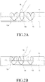
- FIG. 1A is a perspective view of a conventional mutual touch screen panel
- FIG. 1B is a side sectional view taken along line I-I' of FIG. 1A .
- the conventional touch screen panel includes a first electrode layer 11 formed at a lower portion thereof, and a second electrode layer 13 formed above the first electrode layer 11 to be spaced apart from the first electrode layer 11 by a predetermined distance, the second electrode layer 13 being separated from the first electrode layer 11 by a substrate 15 having a certain dielectric coefficient.
- the first electrode layer 11 and the second electrode layer 13 include a plurality of respective electrode lines, such that the electrode lines of the first electrode layer 11 are arranged to cross the electrode lines of the second electrode layer 13.
- a reinforced glass member 17 for protecting the second electrode layer 13 is further provided at an upper portion of the touch screen panel.
- a first circuit (not shown) for applying a signal is connected to the first electrode layer 11. If a signal is applied from the first circuit to the first electrode layer 11, electric fields are created by the signal between the first electrode layer 11 and the second electrode layer 13 and the signal applied to the first electrode layer 11 by the electric fields is transmitted to the second electrode layer 13.
- the signal transmitted to the second electrode layer 13 is provided to a second circuit.
- the second circuit checks a change in the signal transmitted from the second electrode layer 13, checks a touch input, and checks a coordinate value of a region where a touch input is made.
- FIGS. 2A and 2B are side sectional views of the conventional mutual touch screen panel of FIG. 1A , illustrating a state where a finger of a user contacts the mutual touch screen panel.
- a signal of the first electrode layer 11 is coupled to be transmitted to the second electrode layer 13 through the electric fields created between the first electrode layer 11 and the second electrode layer 13 and the signal transmitted from the second electrode layer 13 takes the form of a reference level in the second circuit.
- the finger 18 influences the electric fields created in at least two electrode lines. For example, even if the finger 18 touches a region where the second electrode line 13b is located, as shown in FIG. 2A , the finger 18 also influences the electric fields created by the first electrode line 13a and the third electrode line 13c adjacent to the second electrode line 13b.
- the second circuit connected to the second electrode layer 13 determines a touch region through an interpolation based on the strengths of the outputs of the channels corresponding to the first electrode line 13a, the second electrode line 13b, and the third electrode line 13c. Likewise, if the finger 18 of the user touches a region between the second electrode line 13b and the third electrode line 13c as shown in FIG.
- the second circuit connected to the second electrode layer 13 determines a touch region through an interpolation based on the strengths of the outputs of the channels corresponding to the second electrode line 13b and the third electrode line 13c.
- FIGS. 3A and 3B are side sectional views of the conventional mutual touch screen panel of FIG. 1A , illustrating a state where a stylus pen contacts the conventional mutual touch screen panel.
- an end of a stylus pen used for a touch input is smaller than an end of a finger of a user to form a small contact area, and a diameter of the contact area of the stylus pen 19 may be smaller than the interval among the plurality of electrode lines 13a, 13b, and 13c of the second electrode layer 13.
- the stylus pen 19 if a stylus pen 19 provides a touch input, and in particular if the stylus pen 19 touches a region where the second electrode line 13b is located, the stylus pen 19 only influences the electric fields created by the second electrode line 13b and does not influence the electric fields created by the adjacent first and third electrode lines 13a and 13c as shown in FIG. 3a .
- a diameter of a contact area of the stylus pen 19 is smaller than the interval among the plurality of electrode lines 13a, 13b, and 13c of the second electrode layer 13, to only influence the electric fields created by the second electrode line 13b and not influence the electric fields created by the third electrode line 13c.
- the touch screen panel cannot detect a change of the regions touched by the stylus pen 19.
- an input medium e.g. a stylus pen 19
- the touch screen panel cannot accurately detect a coordinate value of the contact region and cannot detect a change of the regions touched by the input medium (having a contact area smaller than the interval between the plurality of electrode lines)
- an object of the present invention is to address the above-described problems.
- a touch screen panel apparatus includes a first electrode layer that includes a plurality of first electrode lines arranged in a first direction such that adjacent first electrode lines are separated from each other by a predetermined distance; a plurality of first odd-numbered electrode plates coupled to odd-numbered lines of the first electrode lines; and a plurality of first even-numbered electrode plates coupled to even-numbered lines of the first electrode lines, wherein the plurality of first odd-numbered electrode plates and the plurality of first even-numbered electrode plates are alternately arranged in a second direction different from the first direction.
- a touch screen panel apparatus includes a plurality of first electrode layers arranged in a first direction such that adjacent first electrode line are separated from each other by a first distance; and a second electrode layer including a plurality of second electrode lines alternately arranged in a second direction different from the first direction, such that adjacent second electrode lines are separated by a second distance, a plurality of second electrode plates arranged such that adjacent second electrode plates are separated by a third distance along one side of respective second electrode lines, and a plurality of third electrode plates arranged such that adjacent third electrode plates are separated by the third distance, along a side of respective second electrode lines opposite the side to which the second electrode plates are arranged, the plurality of second electrode plates and the plurality of third electrode plates being alternately arranged in the first direction.
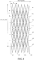
- FIG. 4 is a diagram illustrating a touch screen panel apparatus according to a first embodiment of the present invention.
- the touch screen panel apparatus includes first electrode lines 411, 412, 413, 414, 415, 416, and 417, first electrode plates 41, 42, 43, 44, 45, 46, and 47 formed in a first electrode layer, and second electrode lines 421, 422, 423, and 424 formed in a second electrode layer.
- the first electrode lines 411, 412, 413, 414, 415, 416, and 417 are arranged in a first direction, (e.g. in a longitudinal direction) and are regularly spaced apart from each other by a predetermined distance 'a'.
- the first electrode plates 41, 42, 43, 44, 45, 46, and 47 include first odd-numbered electrode plates 41, 43, 45, and 47 connected to the odd-numbered rows 411, 413, 415, and 417, respectively, of the first electrode line, and first even-numbered electrode plates 42, 44, and 46 connected to the even-numbered rows 412, 414, and 416, respectively, of the first electrode line.
- the first odd-numbered electrode plates 41, 43, 45, and 47 are regularly spaced apart from each other in the odd-numbered rows 411, 413, 415, and 417 of the first electrode line in a second direction, e.g. a transverse direction by a predetermined distance. Moreover, the first odd-numbered electrode plates 41, 43, 45, and 47 and the first even-numbered electrode plates 42, 44, and 46 are alternately arranged in the second direction. That is, the first odd-numbered electrode plates 41, 43, 45, and 47 are arranged in the first column in the second direction, and the first even-numbered electrode plates 42, 44, and 46 are arranged in the second column in the second direction.
- all the first odd-numbered electrode plates connected to the odd-numbered rows 411, 413, 415, and 417 of the first electrode line and all the first even-numbered electrode plates connected to the even-numbered rows 412, 414, and 416 of the first electrode line are regularly arranged.
- each of the first electrode plates 41, 42, 43, 44, 45, 46, and 47 decreases from the center of the first electrode plate to the periphery of the first electrode plate.
- each of the first electrode plates 41, 42, 43, 44, 45, 46, and 47 may have a diamond shape. Since the strengths of the electric fields emitting from an electrode plate become lower as an area of the electrode plate grows smaller, a voltage measured the second electrode layer becomes lower as the location of the voltage measurement further away from the center of the electrode plate. For example, if the distance between each the first electrode lines 411, 412, 413, 414, 415, 416, and 417 are less than a diameter of a contact end of a capacitive touch input pen (i.e.
- the contact end of the touch input pen contacts at least two of the first electrode plates 41, 42, 43, 44, 45, 46, and 47, making it possible to detect an output change according to movement of the touch input pen. Since the first electrode plates 41, 42,43, 44, 45, 46, and 47 are continuously arranged in the first direction, even when the touch input pen contacts a region where only one electrode plate is located, outputs are generated not only in the channel corresponding to the electrode plate but also in the channels corresponding to the adjacent neighboring electrode plates.
- first electrode plates 41, 42, 43, 44, 45, 46, and 47 are illustrated as having a diamond shape in the first embodiment of the present invention, the present invention is not limited thereto. According to embodiments of the present invention, it is sufficient to have first electrode plates of other shapes such that a central portion of each of the first electrode plates 41, 42, 43, 44, 45, 46, and 47 has an area larger than that of a periphery thereof.
- the second electrode lines 421, 422, 423, and 424 are arranged in a second direction, e.g. a transverse direction and are regularly spaced apart from each other by a predetermined distance 'b'.
- the distance 'a' between each of the first electrode lines 411, 412, 413, 414, 415, 416, and 417 may be the same or similar to the distance 'b' between the second electrode lines 421, 422, 423, and 424.
- the first column 421 of the second electrode line can be located in left side of the first odd-numbered electrode plates 41, 43, 45, and 47
- the second column 422 of the second electrode line can be located between second electrode plates and third plates of the first even-numbered electrode plates 41, 43, 45, and 47 in the second direction.
- the third column 423 of the second electrode line can be located between forth electrode plates and fifth plates of the first even-numbered electrode plates in the second direction, and the forth column 424 of the second electrode line can be located in right side of the sixth odd-numbered electrode plates 41, 43, 45, and 47 in the same way.
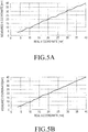
- FIG. 5A and 5B are graphs illustrating a result of an Experiment 1 where touch inputs were provided to the touch screen panel apparatus according to the first embodiment of the present invention.
- FIG. 5A is a graph using measurements obtained by diagonally touching a conventional touch screen panel apparatus are displayed.
- FIG. 5B is a graph using measurements obtained by diagonally touching the touch screen panel apparatus according to the first embodiment of the present invention.
- the X-axis represents X-coordinate values calculated by touch inputs
- the Y-axis represents Y-coordinate values calculated by touch inputs.
- the example of FIG. 5A represents a stepped form due to its low linearity
- the Experiment 1 depicted FIG. 5B represents a relatively high linearity by comparison.
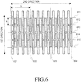
- FIG. 6 is a diagram illustrating a touch screen panel apparatus according to a second embodiment of the present invention.
- the touch screen panel apparatus includes first electrode lines 611, 612, 613, 614, and 615 and first electrode plates 61, 62, 63, 64, and 65 formed in a first electrode layer, and second electrode lines 621, 622, 623, and 624 formed in a second electrode layer.
- the touch screen panel apparatus according to the second embodiment of the present invention is similar the touch screen panel apparatus according to the first embodiment of the present invention.
- a structure of the first electrode plates 61, 62, 63, 64, and 65 coupled to the first electrode lines 611, 612, 613, 614, and 615 differs from the structure of the first electrode plates 41, 42, 43,44, 45, 46, and 47 provided in the touch screen panel apparatus according to the first embodiment of the present invention.
- Each of the first electrode plates 61, 62, 63, 64, and 65 of the touch screen panel apparatus according to the second embodiment of the present invention may have a rectangular shape.
- the length of each of the first electrode plates 61, 62, 63, 64, and 65 in a first direction is preferably longer than the distance 'a' between each of the plurality of first electrode lines 611, 612, 613, 614, and 615.
- the length of each of the first electrode plates 61, 62, 63, 64, and 65 in a first direction is preferably less than twice the distance 'a' between each of the plurality of first electrode lines 611, 612, 613, 614, and 615.
- first electrode plates 61, 62, 63, 64, and 65 may have a rectangular shape in which the length thereof in the first direction is greater than the length thereof in the second direction perpendicular to the first direction.
- the first electrode plates 61, 62, 63, 64, and 65 may include first odd-numbered electrode plates 61, 63, and 65 connected to the odd-numbered rows 611, 613, and 615 of the first electrode line and first even-numbered electrode plates 62 and 64 coupled to the even-numbered rows 612 and 614 of the first electrode line.
- the first odd-numbered electrode plates 61, 63, and 65 and the first even-numbered electrode plates 62 and 64 are alternately arranged continuously in a sensing direction, e.g. the first direction.
- FIGs. 7A and 7B are graphs illustrating a result of an Experiment 2 where touch inputs were provided to the touch screen panel apparatus according to the second embodiment of the present invention.
- FIG. 7A illustrates a graph according to an example, wherein coordinate values are obtained by diagonally touching a conventional touch screen panel apparatus.
- FIG. 7B illustrates a graph according to another example, wherein coordinate values are obtained by diagonally touching the touch screen panel apparatus according to the second embodiment of the present invention.
- the X-axis represents X-coordinate values calculated by touches
- the Y-axis represents Y-coordinate values calculated by touches.
- the comparison example of FIG. 7A shows a stepped form due to low linearity provided by the conventional touch screen apparatus, while Experiment 2 of FIG. 7B shows a relatively high linearity by comparison.
- FIG. 8 is a diagram illustrating a touch screen panel apparatus according to a third embodiment of the present invention.
- the touch screen panel apparatus includes first electrode plates 811, 812, 813, and 814 formed in a first electrode layer, second electrode lines 821, 822, 823, and 824 formed in a second electrode layer, and a second electrode plate 81 and a third electrode plate 82 connected to the second electrode lines 821, 822, 823, and 824.
- the first electrode plates 811, 812, 813, and 814 are arranged in a first direction, (e.g., a longitudinal direction) and are regularly spaced apart from each other by a predetermined distance.
- Each of the first electrode plates 811, 812, 813, and 814 may be a rectangular plate in which the length thereof in the first direction is greater than the length thereof in the second direction.
- the length of each electrode plate in the first direction is large enough to accommodate at least one second electrode plate 81 and at least one third electrode plate 82, that is, is larger than the a height between the second electrode plate 81 and the third electrode plate 82.
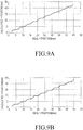
- FIGs. 9A AND 9b are diagrams illustrating a result of an Experiment 3 where touch inputs were provided to the touch screen panel apparatus according to the third embodiment of the present invention.
- FIG. 9A is a graph depicting measurements according to an example, wherein coordinate values are obtained by diagonally touching a conventional touch screen panel apparatus.
- FIG. 9B is a graph depicting measurements according to another example, wherein coordinate values are obtained by diagonally touching the touch screen panel apparatus according to the third embodiment of the present invention.
- the X-axis represents X-coordinate values calculated by touches and the Y-axis represents Y-coordinate values calculated by touches.
- the example of FIG. 9A shows a stepped form due to its low linearity, and, by contrast the example of Experiment 3 in FIG. 9B shows a relatively high linearity.
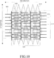
- FIG. 10 is a diagram illustrating a touch screen panel apparatus according to a fourth embodiment of the present invention.
- the touch screen panel apparatus includes a first electrode line 1011 (represented by dashed lines) and first electrode plates 1013 and 1015 formed in a first electrode layer, a second electrode line 1021 (represented by solid lines), a second electrode plate 1023 and a third electrode plate 1025 formed in a second electrode layer.
- the second electrode plate 1023 and the third electrode plate 1025 are connected to the second electrode line 1021.
- the arrangements and structures of the first electrode line 1011 and the first electrode plates 1013 and 1015 are the same as those of the first electrode lines 411, 412, 413, 414, and 415 and the first electrode plate 41, 42, 43, 44, 45, 46, and 47 of the touch screen panel apparatus according to the first embodiment of the present invention.
- the first electrode lines 411, 412, 413, 414, and 415 and the first electrode plate 41, 42, 43, 44, 45, 46, and 47 of the touch screen panel apparatus according to the first embodiment of the present invention can be referred to for details of the first electrode line 1011 and the first electrode plates 1013 and 1015 of the fourth embodiment of the present invention.
- the arrangements and structures of the second electrode line 1021, the second electrode plate 1023, and the third electrode plate 1025 are the same as those of the second electrode lines 821, 822, 823, and 824, the second electrode plate 81, and the third electrode plate 82 of the touch screen panel apparatus according to the third embodiment of the present invention.
- the arrangements and structures of the second electrode line 1021, the second electrode plate 1023, and the third electrode plate 1025 are the same as those of the second electrode lines 821, 822, 823, and 824, the second electrode plate 81, and the third electrode plate 82.
- the second electrode lines 821, 822, 823, and 824 are straight lines, and in Fig.
- the second electrode line 1021 is branched design.
- the second electrode lines 821, 822, 823, and 824 of Fig. 8 and the second electrode line 1021 of Fig. 10 are the same structures.
- the second electrode plate 1023, and the third electrode plate 1025 are the same as those of the second electrode lines 821, 822, 823, and 824, the second electrode plate 81, and the third electrode plate 82 of the touch screen panel apparatus according to the third embodiment of the present invention"
- the second electrode lines 821, 822, 823, and 824, the second electrode plate 81, and the third electrode plate 82 of the touch screen panel apparatus according to the third embodiment of the present invention can be referred to for details of the second electrode line 1021, the second electrode plate 1023, and the third electrode plate 1025, respectively, of the touch screen panel apparatus according to the fourth embodiment of the present invention.
- the quantity and intervals of the first electrode line 1011, the first electrode plates 1013 and 1015, the second electrode line 1021, the second electrode plate 1023, and the third electrode plate 1025 can be variously modified by those skilled in the art, in accordance with embodiments of the present invention.
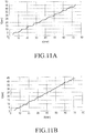
- FIGs. 11A and 11B are graphs illustrating a result of an Experiment 4, where touch inputs were provided the touch screen panel apparatus according to the fourth embodiment of the present invention.
- FIG. 11A is a graph illustrating measurements according to an example, wherein coordinate values obtained by diagonally touching a conventional touch screen panel apparatus.
- FIG. 11B is a graph illustrating measurementsaccording to another example, wherein coordinate values obtained by diagonally touching the touch screen panel apparatus according to the fourth embodiment of the present invention.
- the X-axis represents X-coordinate values calculated by touches
- the Y-axis represents Y-coordinate values calculated by touches.
- the example of FIG. 11A shows a stepped form due to low linearity, and, by contrast FIG. 11B shows a relatively high linearity when using a touch screen according to the fourth embodiment of the present invention.
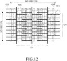
- FIG. 12 is a diagram illustrating a touch screen panel apparatus according to the fifth embodiment of the present invention.
- the touch screen panel apparatus includes a first electrode line 1211 and first electrode plates 1213 and 1215 formed in a first electrode layer, and a second electrode line 1221 formed in a second electrode layer, a second electrode plate 1223, and a third electrode plate 1225.
- the arrangements and structures of the first electrode line 1211 and the first electrode plates 1213 and 1215 are the same as those of the first electrode lines 611, 612, 613, 614, and 615 and the first electrode plates 61, 62, 63, 64, and 65 of the touch screen panel apparatus according to the second embodiment of the present invention.
- the first electrode lines 611, 612, 613, 614, and 615 and the first electrode plates 61, 62, 63, 64, and 65 of the touch screen panel apparatus according to the second embodiment of the present invention can be referred to for details of the first electrode line 1211 and the first electrode plates 1213 and 1215 of the touch screen panel apparatus according to the fifth embodiment of the present invention.
- the arrangements and structures of the second electrode line 1221, the second electrode plate 1223, and the third electrode plate 1225 are the same as those of the second electrode lines 821, 822, 823, and 824, the second electrode plate 81, and the third electrode plate 82 of the touch screen panel apparatus according to the third embodiment of the present invention.
- the second electrode lines 821, 822, 823, and 824, the second electrode plate 81, and the third electrode plate 82 of the touch screen panel apparatus according to the third embodiment of the present invention can be referred to for details of the second electrode line 1221, the second electrode plate 1223, and the third electrode plate 1225 of the touch screen panel apparatus according to the fifth embodiment of the present invention.
- the quantity, intervals, lengths, areas of first electrode lines and first electrode plates formed in a first electrode layer and the quantity, intervals, lengths, areas of second electrode lines, second electrode plates, and third electrode plates formed in a second electrode layer may be variously modified by those skilled in the art.
- a touched region in a touch screen, can be accurately detected without increasing the number of channels.
- a region touched by a user can be accurately detected even if a touch screen panel is touched through an input medium having a contact area smaller than a distance between channels.
Landscapes
- Engineering & Computer Science (AREA)
- General Engineering & Computer Science (AREA)
- Theoretical Computer Science (AREA)
- Human Computer Interaction (AREA)
- Physics & Mathematics (AREA)
- General Physics & Mathematics (AREA)
- Quality & Reliability (AREA)
- Position Input By Displaying (AREA)
Applications Claiming Priority (1)
| Application Number | Priority Date | Filing Date | Title |
|---|---|---|---|
| KR1020110024081A KR20120106165A (ko) | 2011-03-17 | 2011-03-17 | 개선된 전극 구조를 갖는 터치스크린 패널 장치 |
Publications (1)
| Publication Number | Publication Date |
|---|---|
| EP2500804A2 true EP2500804A2 (de) | 2012-09-19 |
Family
ID=45841296
Family Applications (1)
| Application Number | Title | Priority Date | Filing Date |
|---|---|---|---|
| EP12158693A Withdrawn EP2500804A2 (de) | 2011-03-17 | 2012-03-09 | Berührungsbildschirmplattenvorrichtung mit verbesserter Elektrodenstruktur |
Country Status (3)
| Country | Link |
|---|---|
| US (1) | US20120235931A1 (de) |
| EP (1) | EP2500804A2 (de) |
| KR (1) | KR20120106165A (de) |
Cited By (1)
| Publication number | Priority date | Publication date | Assignee | Title |
|---|---|---|---|---|
| WO2017067318A1 (zh) * | 2015-10-22 | 2017-04-27 | 京东方科技集团股份有限公司 | 触摸屏及其驱动方法和显示装置 |
Families Citing this family (5)
| Publication number | Priority date | Publication date | Assignee | Title |
|---|---|---|---|---|
| DK2586933T3 (en) | 2011-10-24 | 2015-12-21 | Areva Wind Gmbh | Work platforms for an offshore wind power plant |
| KR102040973B1 (ko) | 2012-12-14 | 2019-11-06 | 삼성디스플레이 주식회사 | 터치 스크린 패널 |
| KR102075040B1 (ko) | 2013-02-05 | 2020-02-11 | 삼성디스플레이 주식회사 | 터치 스크린 패널 |
| KR101500330B1 (ko) * | 2013-03-12 | 2015-03-10 | 아이티엠 주식회사 | 터치 패널 |
| TWI505167B (zh) * | 2014-02-10 | 2015-10-21 | Quanta Comp Inc | 電容式觸控面板 |
-
2011
- 2011-03-17 KR KR1020110024081A patent/KR20120106165A/ko not_active Withdrawn
-
2012
- 2012-02-08 US US13/368,909 patent/US20120235931A1/en not_active Abandoned
- 2012-03-09 EP EP12158693A patent/EP2500804A2/de not_active Withdrawn
Non-Patent Citations (1)
| Title |
|---|
| None |
Cited By (2)
| Publication number | Priority date | Publication date | Assignee | Title |
|---|---|---|---|---|
| WO2017067318A1 (zh) * | 2015-10-22 | 2017-04-27 | 京东方科技集团股份有限公司 | 触摸屏及其驱动方法和显示装置 |
| US9910525B2 (en) | 2015-10-22 | 2018-03-06 | Boe Technology Group Co., Ltd. | Touch screen and driving method for the same, display apparatus |
Also Published As
| Publication number | Publication date |
|---|---|
| US20120235931A1 (en) | 2012-09-20 |
| KR20120106165A (ko) | 2012-09-26 |
Similar Documents
| Publication | Publication Date | Title |
|---|---|---|
| US9836167B2 (en) | Electrode layout for touch screens | |
| KR101663763B1 (ko) | 터치스크린을 구비한 표시장치 | |
| JP5445438B2 (ja) | 静電容量式タッチパネル | |
| CN104182081B (zh) | 触控感测电极结构及触控装置 | |
| US8922501B2 (en) | Capacitive sensing device comprising cross-shaped sensing elements | |
| US8823666B2 (en) | Touch sensor panel | |
| EP2500804A2 (de) | Berührungsbildschirmplattenvorrichtung mit verbesserter Elektrodenstruktur | |
| US20190294274A1 (en) | Touch screen panel and touch sensing system including the same | |
| JP6076866B2 (ja) | 静電容量型の入力装置 | |
| US20160005352A1 (en) | Touch sensing device | |
| CN104063100B (zh) | 静电电容式触摸板 | |
| JP6284391B2 (ja) | 静電容量型入力装置 | |
| US9645684B2 (en) | Self-capacitive touch panel and conductive layer structure thereof | |
| US20140327845A1 (en) | Touch panel | |
| JP2013225266A (ja) | タッチパネル | |
| KR101540452B1 (ko) | 복수의 접촉 입력을 감지할 수 있는 접촉 감지 패널 및 장치 | |
| US11340729B2 (en) | Touch substrate and display panel | |
| KR101278283B1 (ko) | 터치스크린 장치 | |
| CN104571754B (zh) | 触摸屏、触摸面板以及具有该触摸面板的显示装置 | |
| KR101372329B1 (ko) | 구동전극 패턴, 터치패널, 터치패널 모듈, 및 전자장치 | |
| JPWO2017134718A1 (ja) | タッチセンサ及びそれを備えた入力装置 | |
| TWI611324B (zh) | 觸控結構 | |
| US20150277484A1 (en) | Touch module | |
| KR101097274B1 (ko) | 터치패널센서 | |
| KR101364956B1 (ko) | 터치 패널 센서 |
Legal Events
| Date | Code | Title | Description |
|---|---|---|---|
| PUAI | Public reference made under article 153(3) epc to a published international application that has entered the european phase |
Free format text: ORIGINAL CODE: 0009012 |
|
| AK | Designated contracting states |
Kind code of ref document: A2 Designated state(s): AL AT BE BG CH CY CZ DE DK EE ES FI FR GB GR HR HU IE IS IT LI LT LU LV MC MK MT NL NO PL PT RO RS SE SI SK SM TR |
|
| AX | Request for extension of the european patent |
Extension state: BA ME |
|
| RAP1 | Party data changed (applicant data changed or rights of an application transferred) |
Owner name: SAMSUNG ELECTRONICS CO., LTD. |
|
| STAA | Information on the status of an ep patent application or granted ep patent |
Free format text: STATUS: THE APPLICATION HAS BEEN WITHDRAWN |
|
| 18W | Application withdrawn |
Effective date: 20140402 |