EP2500752A1 - Optisches Element, Lichterkennungsvorrichtung, und Objekterkennungssystem - Google Patents
Optisches Element, Lichterkennungsvorrichtung, und Objekterkennungssystem Download PDFInfo
- Publication number
- EP2500752A1 EP2500752A1 EP12159779A EP12159779A EP2500752A1 EP 2500752 A1 EP2500752 A1 EP 2500752A1 EP 12159779 A EP12159779 A EP 12159779A EP 12159779 A EP12159779 A EP 12159779A EP 2500752 A1 EP2500752 A1 EP 2500752A1
- Authority
- EP
- European Patent Office
- Prior art keywords
- cylindrical face
- axis
- light
- optical element
- infrared ray
- Prior art date
- Legal status (The legal status is an assumption and is not a legal conclusion. Google has not performed a legal analysis and makes no representation as to the accuracy of the status listed.)
- Granted
Links
Images


Classifications
-
- G—PHYSICS
- G02—OPTICS
- G02B—OPTICAL ELEMENTS, SYSTEMS OR APPARATUS
- G02B3/00—Simple or compound lenses
- G02B3/02—Simple or compound lenses with non-spherical faces
- G02B3/06—Simple or compound lenses with non-spherical faces with cylindrical or toric faces
-
- G—PHYSICS
- G01—MEASURING; TESTING
- G01J—MEASUREMENT OF INTENSITY, VELOCITY, SPECTRAL CONTENT, POLARISATION, PHASE OR PULSE CHARACTERISTICS OF INFRARED, VISIBLE OR ULTRAVIOLET LIGHT; COLORIMETRY; RADIATION PYROMETRY
- G01J5/00—Radiation pyrometry, e.g. infrared or optical thermometry
- G01J5/0022—Radiation pyrometry, e.g. infrared or optical thermometry for sensing the radiation of moving bodies
- G01J5/0025—Living bodies
-
- G—PHYSICS
- G01—MEASURING; TESTING
- G01J—MEASUREMENT OF INTENSITY, VELOCITY, SPECTRAL CONTENT, POLARISATION, PHASE OR PULSE CHARACTERISTICS OF INFRARED, VISIBLE OR ULTRAVIOLET LIGHT; COLORIMETRY; RADIATION PYROMETRY
- G01J5/00—Radiation pyrometry, e.g. infrared or optical thermometry
- G01J5/02—Constructional details
- G01J5/08—Optical arrangements
- G01J5/0815—Light concentrators, collectors or condensers
-
- G—PHYSICS
- G02—OPTICS
- G02B—OPTICAL ELEMENTS, SYSTEMS OR APPARATUS
- G02B19/00—Condensers, e.g. light collectors or similar non-imaging optics
- G02B19/0004—Condensers, e.g. light collectors or similar non-imaging optics characterised by the optical means employed
- G02B19/0009—Condensers, e.g. light collectors or similar non-imaging optics characterised by the optical means employed having refractive surfaces only
- G02B19/0014—Condensers, e.g. light collectors or similar non-imaging optics characterised by the optical means employed having refractive surfaces only at least one surface having optical power
-
- G—PHYSICS
- G02—OPTICS
- G02B—OPTICAL ELEMENTS, SYSTEMS OR APPARATUS
- G02B19/00—Condensers, e.g. light collectors or similar non-imaging optics
- G02B19/0033—Condensers, e.g. light collectors or similar non-imaging optics characterised by the use
- G02B19/0076—Condensers, e.g. light collectors or similar non-imaging optics characterised by the use for use with a detector
-
- G—PHYSICS
- G02—OPTICS
- G02B—OPTICAL ELEMENTS, SYSTEMS OR APPARATUS
- G02B19/00—Condensers, e.g. light collectors or similar non-imaging optics
- G02B19/0033—Condensers, e.g. light collectors or similar non-imaging optics characterised by the use
- G02B19/009—Condensers, e.g. light collectors or similar non-imaging optics characterised by the use for use with infrared radiation
-
- G—PHYSICS
- G02—OPTICS
- G02B—OPTICAL ELEMENTS, SYSTEMS OR APPARATUS
- G02B3/00—Simple or compound lenses
- G02B3/0006—Arrays
- G02B3/0037—Arrays characterized by the distribution or form of lenses
- G02B3/0043—Inhomogeneous or irregular arrays, e.g. varying shape, size, height
-
- G—PHYSICS
- G02—OPTICS
- G02B—OPTICAL ELEMENTS, SYSTEMS OR APPARATUS
- G02B3/00—Simple or compound lenses
- G02B3/0006—Arrays
- G02B3/0037—Arrays characterized by the distribution or form of lenses
- G02B3/0062—Stacked lens arrays, i.e. refractive surfaces arranged in at least two planes, without structurally separate optical elements in-between
- G02B3/0068—Stacked lens arrays, i.e. refractive surfaces arranged in at least two planes, without structurally separate optical elements in-between arranged in a single integral body or plate, e.g. laminates or hybrid structures with other optical elements
-
- G—PHYSICS
- G08—SIGNALLING
- G08B—SIGNALLING OR CALLING SYSTEMS; ORDER TELEGRAPHS; ALARM SYSTEMS
- G08B13/00—Burglar, theft or intruder alarms
- G08B13/18—Actuation by interference with heat, light, or radiation of shorter wavelength; Actuation by intruding sources of heat, light, or radiation of shorter wavelength
- G08B13/189—Actuation by interference with heat, light, or radiation of shorter wavelength; Actuation by intruding sources of heat, light, or radiation of shorter wavelength using passive radiation detection systems
- G08B13/19—Actuation by interference with heat, light, or radiation of shorter wavelength; Actuation by intruding sources of heat, light, or radiation of shorter wavelength using passive radiation detection systems using infrared-radiation detection systems
- G08B13/193—Actuation by interference with heat, light, or radiation of shorter wavelength; Actuation by intruding sources of heat, light, or radiation of shorter wavelength using passive radiation detection systems using infrared-radiation detection systems using focusing means
Definitions
- At least one aspect of the present invention relates to at least one of an optical element and a light detection device and an object sensing system.
- Japanese Patent Application Publication No. 2008-128913 discloses an infrared ray detection apparatus characterized by including an infrared ray detection element for detecting an infrared ray, a package for storing the infrared ray detection element, a condenser lens arranged in front of the infrared ray detection element and provided for condensing infrared rays on the infrared ray detection element, and an aberration correction optical element arranged in front of the condenser lens and provided for finely controlling the incident angle of an infrared ray onto the condenser lens to correct for an aberration caused in the condenser lens.
- an optical element capable of condensing light with a broader range of incident angles or a light detection device capable of detecting light with a broader range of incident angles has not been disclosed.
- An object sensing system capable of sensing existence or displacement of an object based on light with a broader range of incident angles has not been disclosed.
- an optical element for condensing light wherein the optical element has a first cylindrical face and a second cylindrical face at one side and a third cylindrical face at an other side and a plane including an axis of the first cylindrical face and an axis of the third cylindrical face intersects with a plane including an axis of the second cylindrical face and the axis of the third cylindrical face.
- a light detection device for detecting light wherein the light detection device includes the optical element as described above and an element for detecting light condensed by the optical element.
- an object sensing system including a light detection device for detecting light from an object and a device for sensing existence or displacement of the object based on light detected by the light detection device, wherein the light detection device is the light detection device as described above.
- a first object of an embodiment of the present invention is to provide an optical element capable of condensing light with a broader range of incident angles.
- a second object of an embodiment of the present invention is to provide a light detection device capable of detecting light with a broader range of incident angles.
- a third object of an embodiment of the present invention is to provide an object sensing system capable of sensing existence or displacement of an object based on light with a broader range of incident angles.
- a first aspect of an embodiment of the present invention is an optical element for condensing light, characterized in that the optical element has a first cylindrical face and a second cylindrical face at one side and a third cylindrical face at an other side and a plane including an axis of the first cylindrical face and an axis of the third cylindrical face intersects with a plane including an axis of the second cylindrical face and the axis of the third cylindrical face.
- a second aspect of an embodiment of the present invention is a light detection device for detecting light, characterized by including the optical element being a first aspect of an embodiment of the present invention and an element for detecting light condensed by the optical element.
- a third aspect of an embodiment of the present invention is an object sensing system, including a light detection device for detecting light from an object and a device for sensing existence or displacement of the object based on light detected by the light detection device, characterized in that the light detection device is the light detection device being a second aspect of an embodiment of the present invention.
- an optical element capable of condensing light with a broader range of incident angles.
- a light detection device capable of detecting light with a broader range of incident angles.
- an object sensing system capable of sensing existence or displacement of an object based on light with a broader range of incident angles.
- FIG. 1A and FIG. 1B are diagrams illustrating one example of an optical element according to a first embodiment of the present invention.
- FIG. 1A is a perspective view illustrating one example of an optical element according to a first embodiment of the present invention.
- FIG. 1B is an elevation view illustrating one example of an optical element according to a first embodiment of the present invention.
- an optical element 100 for condensing light is an optical element 100 for condensing light, wherein such an optical element is characterized in that the optical element 100 has a first cylindrical face 101a and a second cylindrical face 101b at one side and a third cylindrical face 102 at the other side and a plane including an axis C1a of the first cylindrical face 101a and an axis C2 of the third cylindrical face 102 intersects with a plane including an axis C1b of the second cylindrical face 101b and the axis C2 of the third cylindrical face 102.
- a cylindrical face such as, for example, the first cylindrical face 101a, the second cylindrical face 101b, or the third cylindrical face 102, means at least one portion of a solid face composed of parallel generatrices standing on a perimeter of a face. "parallel” includes completely parallel and a degree regarded as substantially parallel.
- an axis of a cylindrical face such as, for example, the axis C1a of the first cylindrical face 101a, the axis C1b of the cylindrical face 101b, or the axis C2 of the third cylindrical face 102, means a set of centers of curvature of lines of intersection of a cylindrical face with planes parallel to a bottom face of a cylinder having a cylindrical face, and is a straight line (or line segment).
- a center of curvature of a cylindrical face such as, for example, a center of curvature of the first cylindrical face 101a, a center of curvature of the second cylindrical face 101b, or a center of curvature of the third cylindrical face 102, is a center of curvature of a line of intersection of a cylindrical face with a plane parallel to a bottom face of a cylinder having a cylindrical face.
- two or three of the axis C1a of the first cylindrical face 101a, the axis C1b of the second cylindrical face 101b, and the axis C2 of the third cylindrical face 102 are not present in an identical or common straight line.
- one side and “the other side” are, for example, a side of entrance of light onto the optical element 100 and a side of exit of light out of the optical element 100, respectively.
- the optical element 100 may be arranged in such a manner that, for example, the first cylindrical face 101a and the second cylindrical face 101b are provided at a side of entrance of light onto the optical element 100 and the third cylindrical face 102 is provided at a side of exit of light from the optical element 100.
- the optical element 100 has the first cylindrical face 101a and the second cylindrical face 101b at one side and the third cylindrical face 102 at the other side, and a plane including the axis C1a of the first cylindrical face 101a and the axis C2 of the third cylindrical face 102 intersects with a plane including the axis C1b of the second cylindrical face 101b and the axis C2 of the third cylindrical face 102.
- a plane including the axis C1a of the first cylindrical face 101a and the axis C2 of the third cylindrical face 102 intersecting with a plane including the axis C1b of the second cylindrical face 101b and the axis C2 of the third cylindrical face 102 means that all of the axis C1a of the first cylindrical face 10a, the axis C1b of the second cylindrical face 101b, and the axis C2 of the third cylindrical face 102, are not present in an identical or common plane.
- the axis C1a of The first cylindrical face 101a and (the axis C1b of) the second cylindrical face 101b are translated (shifted) or rotated toward directions opposite to each other with respect to (the axis C2 of) the third cylindrical face 102.
- first cylindrical face 101a and the second cylindrical face 101b are provided at a side of entrance of light onto the optical element 100 and the third cylindrical face 102 is provided at a side of exit of light from the optical element 100, it may be possible for light with a broader range of incident angles to enter the first cylindrical face 101a and the second cylindrical face 101b and exit from the third cylindrical face 102. It may be possible to divide light with a broader range of incident angles through the first cylindrical face 101a and the second cylindrical face 101b and the third cylindrical face 102 at a higher resolution.
- the optical element 100 capable of condensing light with a broader range of incident angles. According to a first embodiment of the present invention, it may be possible to provide the optical element 100 capable of condensing light at a higher angular resolution.
- a cylindrical face such as the first cylindrical face 101a, the second cylindrical face 101b, or the third cylindrical face 102, in the optical element 100 may be formed by a molding technique using a mold corresponding to a shape of a cylindrical face.
- a cylindrical face such as the first cylindrical face 101a, the second cylindrical face 101b, or the third cylindrical face 102, in the optical element 100 may be formed by using an etching technique for removing a part of a semiconductor wafer.
- An optical element as illustrated in FIG. 1A and FIG. 1B is, for example, capable of being utilized as an optical element included in an infrared light detection device for detecting infrared light from a heat source such as a human body in a house, an office or a car.
- the optical element 100 as illustrated in FIG. 1 A and FIG. 1B is, for example, capable of being utilized as an optical element included in a temperature control device in an air-conditioner, an electromagnetic cooking utensil, or a personal computer or an energy management device for electric power saving.
- a distance between the axis C1a of the first cylindrical face 101a and the axis C2 of the third cylindrical face 102 is identical to a distance between the axis C1b of the second cylindrical face 101b and the axis C2 of the third cylindrical face 102.
- a distance between axes of cylindrical faces such as a distance between the axis C1a of the first cylindrical face 101a and the axis C2 of the third cylindrical face 102 or a distance between the axis C1b of the second cylindrical face 101b and the axis C2 of the third cylindrical face 102 is an average of distances between an axis of one cylindrical face and an axis of the other cylindrical face.
- a distance between an axis of one cylindrical face and an axis of the other cylindrical face is a distance between a point on an axis of one cylindrical face and a point at an intersection of a line perpendicular to an axis of one cylindrical face at a point on an axis of one cylindrical face with an axis of the other cylindrical face.
- each of a distance between the axis C1a of the first cylindrical face 101a and the axis C2 of the third cylindrical face 102 and a distance between the axis C1b of the second cylindrical face 101b and the axis C2 of the third cylindrical face 102 is a value greater than zero.
- the optical element 100 capable of designing an arrangement of the first cylindrical face 101a and the second cylindrical face 101b with respect to the third cylindrical face 102 more easily. It may be possible to provide the optical element 100 capable of being designed more easily and capable of condensing light with a broader range of incident angles. It may be possible to provide the optical element 100 capable of being designed more easily and capable of condensing light at a higher angular resolution.
- a radius of curvature R1a of the first cylindrical face 101a is identical to a radius of curvature R1b of the second cylindrical face 101b.
- a radius of curvature of a cylindrical face such as the radius of curvature R1a of the first cylindrical face 101a or the radius of curvature R1b of the second cylindrical face 101b is a radius of curvature of a line of intersection of a cylindrical face with a plane parallel to a bottom face of a cylinder having a cylindrical face.
- the optical element 100 capable of designing an arrangement of the first cylindrical face 101a and the second cylindrical face 101b with respect to the third cylindrical face 102 more easily. It may be possible to provide the optical element 100 capable of being designed more easily and capable of condensing light with a broader range of incident angles. It may be possible to provide the optical element 100 capable of being designed more easily and capable of condensing light at a higher angular resolution.
- the first cylindrical face 101a and the second cylindrical face 101b are convex faces and the third cylindrical face 102 is a concave face.
- the first cylindrical face 101a and the second cylindrical face 101b are convex faces when viewing from the first cylindrical face 101a and the second cylindrical face 101b to the third cylindrical face 102.
- the third cylindrical face 102 is a concave face when viewing from the third cylindrical face 102 to the first cylindrical face 101a and the second cylindrical face 101b.
- the first cylindrical face 101a and the second cylindrical face 101b have positive powers and the third cylindrical face 102 has a negative power.
- the optical element 100 capable of condensing light with a broader range of incident angles more efficiently. It may be possible to provide the optical element 100 capable of condensing light at a higher angular resolution more efficiently.
- the optical element 100 is formed of a material transparent to an infrared ray.
- An infrared ray includes a near-infrared ray or very-near-infrared ray (an electromagnetic wave with a wavelength greater than or equal to 0.75 ⁇ m and less than or equal to 2 ⁇ m), a normal infrared ray (an electromagnetic wave with a wavelength greater than or equal to 2 ⁇ m and less than or equal to 60 ⁇ m), a mid-infrared ray (an electromagnetic wave with a wavelength greater than or equal to 2 ⁇ m and less than or equal to 20 ⁇ m), a mid-far-infrared ray (an electromagnetic wave with a wavelength greater than or equal to 25 ⁇ m and less than or equal to 60 ⁇ m), and a far-infrared ray (an electromagnetic wave with a wavelength greater than or equal to 25 ⁇ m and less than or equal to 5000 ⁇ m),
- silicon (Si), germanium (Ge), or the like For a material transparent to an infrared ray, there is provided, for example, silicon (Si), germanium (Ge), or the like.
- the optical element 100 When the optical element 100 is formed of a material transparent to an infrared ray, it may be possible to provide the optical element 100 capable of condensing an infrared light with a broader range of incident angles. It may be possible to provide the optical element 100 capable of condensing an infrared light at a higher angular resolution.
- an infrared ray is a far-infrared ray.
- an infrared ray for the optical element 100 is a far-infrared ray
- a material transparent to an infrared ray is a semiconductor material.
- a material transparent to an infrared ray which is a semiconductor material
- a material transparent to an infrared ray is a semiconductor material
- the first cylindrical face 101a and the second cylindrical face 101b have identical or common shapes.
- the optical element 100 capable of being manufactured more easily and capable of condensing light with a broader range of incident angles. It may be possible to provide the optical element 100 capable of being manufactured more easily and capable of condensing light at a higher angular resolution.
- the first cylindrical face 101a and the second cylindrical face 101b are circular cylindrical faces.
- a circular cylindrical face means at least one portion of a solid face composed of parallel generatrices standing on a perimeter of a circle.
- first cylindrical face 101a and the second cylindrical face 101b are circular cylindrical faces, it may be possible to provide the optical element 100 capable of condensing light with a broader range of incident angles more easily. It may be possible to provide the optical element 100 capable of condensing light at a higher angular resolution more easily.
- the first cylindrical face 101a and the second cylindrical face 101b are non-circular cylindrical faces.
- a non-circular cylindrical face means at least one portion of a solid face composed of parallel generatrices standing on a perimeter of a face having a shape other than a circle.
- a non-circular cylindrical face there is provided, for example, a cylindrical face in which a line of intersection of a plane parallel to a bottom face of a cylinder having a cylindrical face with such a cylindrical face is a Gaussian curve, or the like.
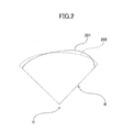
- FIG. 2 is a diagram illustrating another example of an optical element according to a first embodiment of the present invention.
- a first and second cylindrical faces 201 are non-circular cylindrical faces.
- a center of curvature of a line of intersection of a cylindrical face with a plane parallel to a bottom face of a cylinder having a cylindrical face is a center of curvature C of an arc 202 which best approximates a line of intersection of a cylindrical face with a plane parallel to a bottom face of a solid having a cylindrical face.
- a radius of curvature of a line of intersection of a cylindrical face with a plane parallel to a bottom face of a cylinder having a cylindrical face is a radius of curvature R of the arc 202 which best approximates a line of intersection of a cylindrical face with a plane parallel to a bottom face of a cylinder having a cylindrical face.
- the arc 202 which best approximates a line of intersection of a cylindrical face with a plane parallel to a bottom face of a cylinder having a cylindrical face, by means of approximation of an arc for a design value of the first or second cylindrical faces 201 being a non-circular cylindrical face or a line of intersection of a cylindrical face with a plane parallel to a bottom face of a cylinder having a cylindrical face based on a least-square method.
- first cylindrical face 101a and the second cylindrical face 101b are non-circular cylindrical faces
- a shape of the first cylindrical face 101a or the second cylindrical face 101b being a non-circular cylindrical face is adjusted whereby it may be possible to reduce aberration of light condensed by the optical element 100.
- the optical element 100 capable of condensing light with a broader range of incident angles and capable of reducing aberration of condensed light.
- the optical element 100 capable of condensing light at a higher angular resolution and capable of reducing aberration of condensed light.
- the first cylindrical face 101a and the second cylindrical face 101b are perpendicular to a plane H including the axis C1a of the first cylindrical face 101a and the axis C1b of the second cylindrical face 101b and have symmetric shapes with respect to a plane V including the axis C2 of the third cylindrical face 102.
- symmetric includes completely symmetric and a degree regarded as substantially symmetric.
- the optical element 100 capable of being designed or manufactured more easily and capable of condensing light with a broader range of incident angles. It may be possible to provide the optical element 100 capable of being designed or manufactured more easily and capable of condensing light at a higher angular resolution.
- the optical element 100 has a first plane provided with the first cylindrical face 101a and a second plane provided with the second cylindrical face 101b and a first plane and a second plane are planes inclined with respect to the plane H including the axis C1a of the first cylindrical face 101a and the axis C1b of the second cylindrical face 101b.
- a plane such as a first plane or a second plane includes a complete plane and a curved face or convex or concave face regarded as a substantial plane.
- a first plane and a second plane being planes inclined with respect to the plane H including the axis C1a of the first cylindrical face 101a and the axis C1b of the second cylindrical face 101b means that angles of a first plane and a second plane with respect to the plane H including the axis C1a of the first cylindrical face 101a and the axis C1b of the second cylindrical face 101b are angles greater than 0 degrees and less than 90 degrees.
- the optical element 100 has a first plane provided with the first cylindrical face 101a and a second plane provided with the second cylindrical face 101b and a first plane and a second plane are planes inclined with respect to the plane H including the axis C1a of the first cylindrical face 101a and the axis C1b of the second cylindrical face 101b, it may be possible to provide the optical element 100 capable of being designed more easily and capable of condensing light with a broader range of incident angles. It may be possible to provide the optical element 100 capable of being designed more easily and capable of condensing light at a higher angular resolution.
- a first plane and a second plane have symmetric shapes with respect to the plane V which is perpendicular to the plane H including the axis C1a of the first cylindrical face 101a and the axis C1b of the second cylindrical face 101b and includes the axis C2 of the third cylindrical face 102.
- symmetric includes completely symmetric and a degree regarded as substantially symmetric.
- first plane and a second plane have symmetric shapes with respect to the plane V which is perpendicular to the plane H including the axis C1a of the first cylindrical face 101a and the axis C1b of the second cylindrical face 101b and includes the axis C2 of the third cylindrical face 102
- the optical element 100 capable of being manufactured more easily and capable of condensing light with a broader range of incident angles. It may be possible to provide the optical element 100 capable of being manufactured more easily and capable of condensing light at a higher angular resolution.
- a maximum value of a length of the optical element 100 in a direction perpendicular to the plane H including the axis C1a of the first cylindrical face 101a and the axis C1b of the second cylindrical face 101b is less than or equal to 1 mm.
- a maximum value of a length of the optical element 100 in a direction perpendicular to the plane H including the axis C1a of the first cylindrical face 101a and the axis C1b of the second cylindrical face 101b is less than or equal to 1 mm, it may be possible to provide the optical element 100 being capable of condensing light with a broader range of incident angles and being more compact. It may be possible to provide the optical element 100 being capable of condensing light at a higher angular resolution and being more compact.
- the first cylindrical face 101a and the second cylindrical face 101b have Fresnel lens shapes.
- a Fresnel lens shape is a shape obtained by dividing the first cylindrical face 101a (or the second cylindrical face 101b) being a continuous curved face by plural lines parallel to the axis C1a of the first cylindrical face 101a (or the axis C1b of the second cylindrical face 101b) and reducing a distance(s) (or thickness) from a surface of the first cylindrical face 101a (or the second cylindrical face 101b) at an opposite side to a divided part(s) of the first cylindrical face 101a (or the second cylindrical face 101b).
- a Fresnel lens shape is a shape including plural cylindrical faces with a curvature of a portion of the first cylindrical face 101a (or the second cylindrical face 101b).
- a Fresnel lens shape is a sawtooth shape with a curvature of a portion of the first cylindrical face 101a (or the second cylindrical face 101b) in a cross-section perpendicular to the axis C1a of the first cylindrical face 101a (or the axis C1b of the second cylindrical face 101b).
- parallel includes completely parallel and a degree regarded as substantially parallel.
- perpendicular includes completely perpendicular and a degree regarded as substantially perpendicular.
- FIG. 11 is a diagram illustrating yet another example of an optical element according to a first embodiment of the preset invention.
- An optical element 1100 as illustrated in FIG. 11 has a first or second cylindrical face 1101 having a Fresnel lens shape.
- a Fresnel lens shape of a first cylindrical face or second cylindrical face as illustrated by curved lines and a solid and straight line connecting curved lines in FIG. 11 is a shape obtained by dividing a cylindrical face 1102 having a shape of a single convex curved face as illustrated by a dotted line in FIG.
- a Fresnel lens shape of a first cylindrical face or second cylindrical face is a shape including plural cylindrical faces with a curvature of a portion of a first cylindrical face or second cylindrical face.
- a Fresnel lens shape of a first cylindrical face or second cylindrical face is a saw-tooth shape with a curvature of a portion of a first cylindrical face or second cylindrical face in a cross-section perpendicular to an axis of a first cylindrical face or second cylindrical face.
- the cylindrical face 1102 having a shape of a single curved face is a non-circular cylindrical face which is asymmetric with respect to a plane perpendicular to an axis of a third cylindrical face as illustrated by a longitudinal dotted and straight line in FIG. 11 .
- a Fresnel lens shape of a first cylindrical face or second cylindrical face is a non-circular cylindrical face which is asymmetric with respect to a plane perpendicular to an axis of a third cylindrical face as illustrated in a longitudinal dotted and straight line in FIG. 11 .
- a thickness of a Fresnel lens shape (a maximum thickness of a first cylindrical face or second cylindrical face in a direction perpendicular to a plane including an axis of a cylindrical face and an axis of a second cylindrical face: amount of sag) is appropriately determined depending on a condition of designing or manufacturing of an optical element and is not particularly limited.
- first cylindrical face 101a and the second cylindrical face 101b in the optical element 100 have Fresnel lens shapes, it may be possible to reduce a maximum thickness of the first cylindrical face 101a or the second cylindrical face 101b in a direction perpendicular to a plane including the axis C1a of the first cylindrical face 101a and the axis C1b of the second cylindrical face 101b (amount of sag).
- a maximum thickness of the first cylindrical face 101a or the second cylindrical face 101b in a direction perpendicular to a plane including the axis C1a of the first cylindrical face 101a and the axis C1b of the second cylindrical face 101b (amount of sag)
- the first cylindrical face 101a or the second cylindrical face 101b When it may be possible to reduce a maximum thickness of the first cylindrical face 101a or the second cylindrical face 101b in a direction perpendicular to a plane including the axis C1a of the first cylindrical face 101a and the axis C1b of the second cylindrical face 101b (amount of sag), it may be possible to, for example, reduce damage of the optical element 100 pressed in a pressing process when a wafer for forming an optical element and a wafer for forming an element for detecting light condensed by the optical element 100 included in a light detection device are bonded to each other.
- first cylindrical face 101a and the second cylindrical face 101b in the optical element 100 have Fresnel lens shapes, it may be possible to provide the optical element 100 capable of condensing light with a broader range of incident angles. Even when the first cylindrical face 101a and the second cylindrical face 101b in the optical element 100 have Fresnel lens shapes, it may be possible to provide the optical element 100 capable of condensing light at a higher angular resolution.
- FIG. 3 is a diagram illustrating a general structure of a first example of a light detection device according to a second embodiment of the present invention.
- a first example of a light detection device according to a second embodiment of the present invention as illustrated in FIG. 3 is a light detection device 300 for detecting light, wherein a light detection device is characterized by including an optical element according to a first embodiment of the present invention and an element 304 for detecting light condensed by an optical element.
- the light detection device 300 as illustrated in FIG. 3 includes an optical element according to a first embodiment of the present invention as illustrated in FIG. 1A and FIG. 1B and the element (optical sensor) 304 for detecting light condensed by an optical element.
- An optical element as illustrated in FIG. 3 has a first cylindrical face 301a and a second cylindrical face 301b at one side and a third cylindrical face 302 at the other side and a plane including an axis of the first cylindrical face 301a and an axis of the third cylindrical face 302 intersects with a plane including an axis of the second cylindrical face 301b and an axis of the third cylindrical face 302.
- An optical element as illustrated in FIG. 3 has a first cylindrical face 301a and a second cylindrical face 301b at one side and a third cylindrical face 302 at the other side and a plane including an axis of the first cylindrical face 301a and an axis of the third cylindrical face 302 intersects with a plane including an axis of the second cylindrical face 301b and an axis of the third cylindrical face 302.
- a support substrate 303 for supporting a part having the first cylindrical face 301a, the second cylindrical face 301b, and the third cylindrical face 302 (a substrate to be provided with a part having the first cylindrical face 301a, the second cylindrical face 301b, and the third cylindrical face 302) in addition to the first cylindrical face 301a, the second cylindrical face 301b, and the third cylindrical face 302.
- (a maximum value of) a length Y of an optical element in a direction perpendicular to a plane including an axis of the first cylindrical face 301a and an axis of the second cylindrical face 301b as illustrated in FIG. 1A and FIG. 1B is less than or equal to 1 mm.
- (a maximum value of) the length Y of an optical element in a direction perpendicular to a plane including an axis of the first cylindrical face 301a and an axis of the second cylindrical face 301b is a distance from a straight line on a top of the first cylindrical face 301a or the second cylindrical face 301b to a plane of the support substrate 303 at a side of a circuit board 305.
- the optical sensor 304 receives light condensed by an optical element and converts received light into an electric signal, and thereby, light condensed by an optical element is detected.
- the optical sensor 304 includes a light receiving surface (pixel) for receiving light condensed by an optical element and a circuit (sensor circuit) for converting light received by a light receiving surface into an electric signal.
- a light receiving surface is a layer (infrared ray absorption layer) which absorbs and converts infrared light condensed by an optical element into heat
- a sensor circuit is an element for converting heat converted by a light receiving surface into an electric signal.
- the optical sensor 304 may be provided on a cavity structure 306 formed on the circuit board 305.
- the optical sensor 304 outputs a signal (electric signal) related to light detected by the optical sensor 304.
- a signal electrical signal
- the optical device 300 as illustrated in FIG. 3 may further include a circuit part 307 which includes a signal amplification circuit for amplifying a signal output from the optical sensor 304 and a signal processing circuit for processing a signal amplified by a signal amplification circuit.
- the circuit part 307 is provided on the circuit board 305.
- a signal amplification circuit included in the circuit part 307 may be a circuit for amplifying an electric signal output from an optical sensor for infrared light detected by the optical sensor 304 and a signal processing circuit included in the circuit part 307 may be a circuit for obtaining information of an incident angle of infrared light incident on an optical element or presence or absence or a direction of a heat source for generating infrared light incident on an optical element (or light source), from a signal amplified by a signal amplification circuit.
- the optical sensor 304 and the circuit part 307 provided on the cavity structure 306 are provided adjacent to the circuit board 305, and therefore, it may be possible to provide a more compact light detection device 300.
- the light detection device 300 includes an optical element according to a first embodiment of the present invention, and therefore, it may be possible for light with a broader range of incident angles to enter the first cylindrical face 301a and the second cylindrical face 301b and exit from the third cylindrical face 302. It may be possible to divide light with a broader range of incident angles through the first cylindrical face 301a and the second cylindrical face 301b and the third cylindrical face 302 at a higher resolution.
- the light detection device 300 capable of detecting light with a broader range of incident angles. According to a second embodiment of the present invention, it may be possible to provide the light detection device 300 capable of detecting light at a higher angular resolution.
- the light detection device 300 as illustrated in FIG. 3 is capable of being utilized as, for example, an infrared light detection device for detecting infrared light from a heat source such as a human body in a house, an office, or a car or the like.
- the light detection device 300 as illustrated in FIG. 3 is capable of being utilized as, for example, a temperature control device in an air-conditioner, an electromagnetic cooking utensil, or a personal computer or an energy management device for electric power saving.
- an optical element and a light detecting element are formed of a semiconductor material.
- silicon Si
- Si silicon
- an optical element and a light detecting element are formed of a semiconductor material, it may be possible to manufacture the light detection device 300 more easily by using a semiconductor process. It may be possible to provide the light detection device 300 capable of being manufactured more easily and capable of detecting light with a broader range of incident angles. According to a second embodiment of the present invention, it may be possible to provide the light detection device 300 capable of being manufactured more easily and capable of detecting light at a higher angular resolution.
- FIG. 4A, FIG. 4B, and FIG. 4C are diagrams illustrating a more detailed structure of a first example of a light detection device according to a second embodiment of the present invention.
- FIG. 4A is a plan view of a first example of a light detection device according to a second embodiment of the present invention.
- FIG. 4B is a cross-sectional view of a first example of a light detection device according to a second embodiment of the preset invention in direction of AA'.
- FIG. 4C is a cross-sectional view of a first example of a light detection device according to a second embodiment of the present invention in a direction of BB'.
- a first example of a light detection device according to a second embodiment of the present invention as illustrated in FIG. 4A, FIG. 4B, and FIG. 4C is an infrared light sensor 400 similar to a light detection device 300 according to a second embodiment of the present invention as illustrated in FIG. 3 .
- the infrared light sensor 400 as illustrated in FIG. 4A, FIG. 4B, and FIG. 4C is an infrared light device for detecting infrared light and includes an infrared ray condensing element as an optical element according to a first embodiment of the present invention and a sensor circuit 403 as an element for detecting infrared light condensed by an infrared ray condensing element.
- the sensor circuit 403 is held by a circuit board 404.
- the sensor circuit 403 has plural infrared ray receiving surfaces (pixels) which are arranged one-dimensionally and receive infrared light, and converts an infrared light received by an infrared ray receiving surface into an electric signal.
- the infrared light sensor 400 includes a signal amplification circuit for amplifying an electric signal output from the sensor circuit 403 and a signal processing circuit for obtaining information of presence or absence or a direction of a heat source from an output of a signal amplification circuit.
- An infrared ray condensing element included in the infrared light sensor 400 is an optical element for condensing infrared light.
- An infrared ray condensing element condenses infrared light radiated from a heat source onto an infrared ray receiving surface (pixel) of the sensor circuit 403 depending on an incident angle of an infrared light ray.
- An infrared ray condensing element is formed of a semiconductor material transparent to an infrared ray, such as silicon (Si) or germanium (Ge).
- Silicon (Si) is a material transparent to infrared light with a wavelength of about 10 ⁇ m.
- silicon (Si) is used for a material transparent to infrared light.
- silicon (Si) is used as a material transparent to infrared light, not only may it be possible to form an infrared ray condensing element of silicon (Si) but it may also be possible to form the sensor circuit 403, a signal amplification circuit, and a signal processing circuit by using a CMOS process technique.
- An infrared ray condensing element has a first cylindrical face 401a and a second cylindrical face 401b at a side of entrance of an infrared ray and a third cylindrical face 402 at a side of exit of an infrared ray.
- the first cylindrical face 401a and the second cylindrical face 401b are convex and circular cylindrical faces having identical or common shapes and the third cylindrical face 402 is a concave and circular cylindrical face.
- a plane including an axis of the first cylindrical face 401a and an axis of the third cylindrical face 402 intersects with a plane including an axis of the second cylindrical face 401b and an axis of the third cylindrical face 402.
- a distance between an axis of the first cylindrical face 401a and an axis of the third cylindrical face 402 is identical to a distance between an axis of the second cylindrical face 401b and an axis of the third cylindrical face 402.
- a radius of curvature of the first cylindrical face 401a is identical to a radius of curvature of the second cylindrical face 401b.
- the first cylindrical face 401a and the second cylindrical face 401b have symmetric shapes with respect to a plane which is perpendicular to a plane including an axis of the first cylindrical face 401a and an axis of the second cylindrical face 401b and includes an axis of the third cylindrical face 402.
- the first cylindrical face 401a and (an axis of) the second cylindrical face 401b are shifted by a predetermined amount Z with respect to a plane which is perpendicular to a plane including an axis of the first cylindrical face 401a and an axis of the second cylindrical face 401b and includes an axis of the third cylindrical face 402.
- a direction of the axis of first cylindrical face 401a or the axis of second cylindrical face 401b is a direction orthogonal to a direction of arrangement of light receiving surfaces (pixels) of the sensor circuit 403 arranged one-dimensionally (a parallel to AA').
- the first cylindrical face 401a and the second cylindrical face 401b are mutually shifted in a direction of arrangement of one-dimensionally arranged light receiving surfaces (pixels) of the sensor circuit 403 (a direction parallel to AA').
- a distance between the third cylindrical face 402 and the sensor circuit 403 is adjusted by reducing a size of a spot of infrared light condensed on a light receiving surface of the sensor circuit 403.
- the third cylindrical face 402 may have a concave shape engraved on an infrared ray condensing element to reduce a size of a spot of infrared light condensed on a light receiving surface of the sensor circuit 403.
- the first cylindrical face 401a, the second cylindrical face 401b, and the third cylindrical face 402 in an infrared ray condensing element are preferably provided with an anti-reflection coating which is composed of a single layer film or multilayer film transmitting infrared light.
- an anti-reflection coating which is composed of a single layer film or multilayer film transmitting infrared light
- infrared light When an infrared ray radiated from a heat source enters an infrared ray condensing element of the infrared light sensor 400, infrared light transmits through the first cylindrical face 401a or the second cylindrical face 401b and is refracted by either the first cylindrical face 401a or the second cylindrical face 401b. Infrared light having been transmitted through the first cylindrical face 401a or the second cylindrical face 401b enters the second cylindrical face 402. Infrared light having entered the second cylindrical face 402 is refracted by the second cylindrical face 402 and exits from an infrared ray condensing element. Infrared light exiting from an infrared ray condensing element is condensed on a predetermined light receiving surface (pixel) in the sensor circuit 403 at a relatively short distance.
- pixel light receiving surface
- a size of the infrared light sensor 400 is often sufficiently small compared to a distance from the infrared light sensor 400 to a heat source, and therefore, it may often be possible to regard infrared light entering the infrared light sensor 400 as parallel rays of infrared light.
- infrared light entering the infrared light sensor 400 is parallel rays of infrared light.
- an infrared ray condensing element has the first cylindrical face 401a and the second cylindrical face 401b, and therefore, it may be possible to receive parallel rays of infrared light with two different incident angles on one light receiving surface (pixel) of the sensor circuit 403 included in the infrared light sensor 400.
- the sensor circuit 403 included in the infrared light sensor 400 has N light receiving surface(s) (pixel(s)), it may be possible to receive parallel rays of infrared light with 2N different incident angles on N light receiving surface(s) (pixel(s)) of the sensor circuit 403 included in the infrared light sensor 400, because an infrared ray condensing element has the first cylindrical face 401a and the second cylindrical face 401b.
- an infrared ray condensing element included in the infrared light sensor 400 as illustrated in FIG. 4A, FIG. 4B, and FIG. 4C , it may be possible to provide an infrared ray condensing element capable of condensing light with a broader range of incident angles and an infrared light sensor capable of detecting light with a broader range of incident angles, even when the sensor circuit 403 with a relatively few pixel(s) is/are provided. It may be possible to provide an infrared ray condensing element capable of condensing light at a higher angular resolution and an infrared light sensor capable of detecting light at a higher angular resolution. It may be possible to provide an infrared light sensor capable of obtaining information of presence or absence or a direction of a heat source at a higher precision.
- An infrared ray condensing element further includes a support substrate 405 for supporting a part having the first cylindrical face 401a and second cylindrical face 401b and the third cylindrical face 402. A part having the first cylindrical face 401a and the second cylindrical face 401b and the third cylindrical face 402 are bonded to the support substrate 405. The support substrate 405 is bonded to the circuit board 404.
- the circuit board 404 holds the sensor circuit 403, a signal amplification circuit, and a signal processing circuit, and packages the sensor circuit 403, a signal amplification circuit, and a signal processing circuit together with a part having the first cylindrical face 401a and the second cylindrical face 401b and the third cylindrical face 402 and the support substrate 405.
- a length of an infrared ray condensing element in a direction perpendicular to a plane including an axis of the first cylindrical face 401a and an axis of the second cylindrical face 401b, that is, a distance between a straight line of a top of the first cylindrical face 401a or the second cylindrical face 401b and a bonding face of the circuit board 404 and the support substrate 405, is less than or equal to 1 mm, and therefore, it may be possible to provide a more compact infrared light sensor 400.
- the first cylindrical face 401a, the second cylindrical face 401b, and the third cylindrical face 402 in an infrared ray condensing element included in the infrared light sensor 400 may be formed by a molding technique using a mold corresponding to a shape of an infrared ray condensing element.
- the infrared light sensor 400 may be manufactured by a method including forming an infrared ray condensing element from a first semiconductor wafer, forming the sensor circuit 403, a signal amplification circuit, and a signal processing circuit from a second semiconductor wafer, bonding a first semiconductor wafer with a formed infrared ray condensing element and a second semiconductor wafer with the formed sensor circuit 403, signal amplification circuit, and signal processing circuit, and cutting a bonded first semiconductor wafer and second semiconductor wafer. It may be possible to manufacture the infrared light sensor 400 from a semiconductor wafer by using a semiconductor wafer process.
- the first cylindrical face 401a, the second cylindrical face 401b, and the third cylindrical face 402 in an infrared ray condensing element are formed by using an etching technique for eliminating a portion of a first semiconductor wafer.
- the sensor circuit 403, a signal amplification circuit, and a signal processing circuit are formed by using an etching technique for eliminating a portion of a second semiconductor wafer. It may be possible to manufacture the infrared light sensor 400 with a lower cost and a higher productivity.
- the infrared light sensor 400 may be used as, for example, a motion sensor.
- FIG. 9A and FIG. 9B are diagrams illustrating an example of a ray incident on an optical element in a first example of a light detection device according to a second embodiment of the present invention.
- FIG. 9A is a diagram illustrating an example of a ray incident on a first cylindrical face of an optical element in a first example of a light detection device according to a second embodiment of the present invention.
- FIG. 9B is a diagram illustrating an example of a ray incident on a second cylindrical face of an optical element in a first example of a light detection device according to a second embodiment of the present invention.
- a first example of a light detection device according to a second embodiment of the present invention as illustrated in FIG. 9A and FIG. 9B is an infrared light sensor 900 similar to the light detection device 400 according to a second embodiment of the present invention as illustrated in FIG. 4A, FIG. 4B, and FIG. 4C .
- the infrared light sensor 900 as illustrated in FIG. 9A and FIG. 9B is a light detection device for detecting infrared light and includes an infrared ray condensing element as an optical element according to a first embodiment of the present invention and a sensor circuit as an element for detecting infrared light condensed by an infrared ray condensing element.
- an infrared ray condensing element has a first cylindrical face 901a and a second cylindrical face 901b at one side and a third cylindrical face 902 at the other side.
- the first cylindrical face 901a and the second cylindrical face 901b are convex and circular cylindrical faces having identical or common shapes and the third cylindrical face 902 is a concave and circular cylindrical face.
- a plane including an axis of the first cylindrical face 901a and an axis of the third cylindrical face 902 intersects with a plane including an axis of the second cylindrical face 901b and an axis of the third cylindrical face 902.
- a distance between an axis of the first cylindrical face 901a and an axis of the third cylindrical face 902 is identical to a distance between an axis of the second cylindrical face 901b and an axis of the third cylindrical face 902.
- a radius of curvature of the first cylindrical face 901a is identical to a radius of curvature of the second cylindrical face 901b.
- the first cylindrical face 901a and the second cylindrical face 901b have symmetric shapes with respect to a plane which is perpendicular to a plane including an axis of the first cylindrical face 901a and an axis of the second cylindrical face 901b and includes an axis of the third cylindrical face 902.
- the first cylindrical face 901a and (an axis of) the second cylindrical face 901b are shifted by a predetermined amount with respect to a plane which is perpendicular to a plane including an axis of the first cylindrical face 901a and an axis of the second cylindrical face 901b and includes an axis of the third cylindrical face 902.
- An infrared ray condensing element condenses infrared light incident on an infrared ray condensing element in a direction parallel to at least one of directions of an axis of the first cylindrical face 901a, an axis of the second cylindrical face 901b, and an axis of the third cylindrical face 902. "parallel" includes completely parallel and a degree regarded as substantially parallel.
- a sensor circuit includes plural infrared ray receiving surfaces (pixels) 903 as plural elements for receiving light condensed by an infrared ray condensing element in a direction orthogonal to at least one of directions of an axis of the first cylindrical face 901a, an axis of the second cylindrical face 901b, and an axis of the third cylindrical face 902. "orthogonal" includes completely orthogonal and a degree regarded as substantially orthogonal.
- a sensor circuit including the plural infrared ray receiving surfaces (pixels) 903 is a one-dimensional array sensor.
- infrared rays radiated from a heat source (light source) which may be considered to be present at infinity are incident on the infrared light sensor 900 as parallel rays.
- An infrared ray incident on the infrared light sensor 900 is condensed by an infrared ray condensing element and a condensed infrared ray may be received by one infrared ray receiving surface 903 included in a sensor circuit.
- an infrared ray radiated from a heat source when incident on the first cylindrical face 901a at a relatively large angle ⁇ 1 with respect to a direction perpendicular to a plane including an axis of the first cylindrical face 901a and axis of the second cylindrical face 901b of an infrared ray condensing element, an infrared ray radiated from a heat source transmits through the first cylindrical face 901a and the third cylindrical face 902 of an infrared ray condensing element and is refracted by the first cylindrical face 901a and the third cylindrical face 902 of an infrared ray condensing element.
- an infrared ray radiated from a heat source when incident on the first cylindrical face 901a at a relatively small angle ⁇ 2 with respect to a direction perpendicular to a plane including an axis of the first cylindrical face 901a and axis of the second cylindrical face 901b of an infrared ray condensing element, an infrared ray radiated from a heat source transmits through the first cylindrical face 901a and the third cylindrical face 902 of an infrared ray condensing element and is refracted by the first cylindrical face 901a and the third cylindrical face 902 of an infrared ray condensing element.
- An infrared ray incident on the first cylindrical face 901a at an angle ⁇ 2 is condensed on the infrared ray receiving surface (pixel) 903 at the other end included in a sensor circuit.
- an infrared ray radiated from a heat source When an infrared ray radiated from a heat source is incident on the first cylindrical face 901a at an angle greater than ⁇ 2 and less than ⁇ 1 with respect to a direction perpendicular to a plane including an axis of the first cylindrical face 901a and an axis of the second cylindrical face 901b of an infrared ray condensing element, an infrared ray radiated from a heat source transmits through the first cylindrical face 901a and the third cylindrical face 902 of an infrared ray condensing element and is refracted by the first cylindrical face 901a and the third cylindrical face 902 of an infrared ray condensing element.
- An infrared ray incident on a the first cylindrical face 901a at an angle greater than ⁇ 2 and less than ⁇ 1 1 is condensed on the infrared ray receiving surface (pixel) 903 between one end and the other end included in a sensor circuit.
- an infrared ray radiated from a heat source When an infrared ray radiated from a heat source is incident on the second cylindrical face 901b at an angle greater than or equal to ⁇ 2 and less than or equal to ⁇ 1 with respect to a direction perpendicular to a plane including an axis of the first cylindrical face 901a and axis of the second cylindrical face 901b of an infrared ray condensing element, an infrared ray radiated from a heat source transmits through the second cylindrical face 901b and the third cylindrical face 902 of an infrared ray condensing element and is refracted by the second cylindrical face 901b and the third cylindrical face 902 of an infrared ray condensing element.
- An infrared ray incident on the second cylindrical face 901b at an angle greater than or equal to ⁇ 2 and less than ⁇ 1 or equal to is not condensed on the infrared ray receiving surface (pixel) 903 included in
- an infrared ray radiated from a heat source when incident on the second cylindrical face 901b at a relatively large angle ⁇ 3 (at an opposite side with respect to an angle ⁇ 1 or 02) with respect to a direction perpendicular to a plane including an axis of the first cylindrical face 902a and axis of the second cylindrical face 901b of an infrared ray condensing element, an infrared ray radiated from a heat source transmits through the second cylindrical face 901b and the third cylindrical face 902 of an infrared ray condensing element and is refracted by the second cylindrical face 901b and the third cylindrical face 902 of an infrared ray condensing element.
- An infrared ray incident on the second cylindrical face 901b at an angle ⁇ 3 is condensed on the infrared ray receiving surface (pixel) 903 at one end included in a sensor circuit.
- an infrared ray radiated from a heat source when incident on the second cylindrical face 901b at a relatively small angle ⁇ 4 (at an opposite side with respect to an angle ⁇ 1 or ⁇ 2) with respect to a direction perpendicular to a plane including an axis of the first cylindrical face 901a and axis of the second cylindrical face 901b of an infrared ray condensing element, an infrared ray radiated from a heat source transmits through the second cylindrical face 901b and the third cylindrical face 902 of an infrared ray condensing element and is refracted by the second cylindrical face 901b and the third cylindrical face 902 of an infrared ray condensing element.
- An infrared ray incident on the second cylindrical face 901b at an angle ⁇ 4 is condensed on the infrared ray receiving surface (pixel) 903 at the other end included in a sensor circuit.
- an infrared ray radiated from a heat source When an infrared ray radiated from a heat source is incident on the second cylindrical face 901b at an angle greater than ⁇ 4 and less than ⁇ 3 with respect to a direction perpendicular to a plane including an axis of the first cylindrical face 901a and an axis of the second cylindrical face 901b of an infrared ray condensing element, an infrared ray radiated from a heat source transmits through the second cylindrical face 901b and the third cylindrical face 902 of an infrared ray condensing element and is refracted by the second cylindrical face 901b and the third cylindrical face 902 of an infrared ray condensing element.
- An infrared ray incident on the second cylindrical face 901b at an angle greater than ⁇ 4 and less than ⁇ 3 is condensed on the infrared ray receiving surface (pixel) 903 between one end and the other end included in a sensor circuit.
- an infrared ray radiated from a heat source When an infrared ray radiated from a heat source is incident on the first cylindrical face 901a at an angle greater than or equal to ⁇ 4 and less than or equal to ⁇ 3 with respect to a direction perpendicular to a plane including an axis of the first cylindrical face 901a and an axis of the second cylindrical face 901b of an infrared ray condensing element, an infrared ray radiated from a heat source transmits through the first cylindrical face 901a and the third cylindrical face 902 of an infrared ray condensing element and is refracted by the first cylindrical face 901b and the third cylindrical face 902 of an infrared ray condensing element.
- An infrared ray incident on the first cylindrical face 901a at an angle greater than or equal to ⁇ 4 and less than or equal to ⁇ 3 is not condensed on the infrared ray receiving surface (pixel) 903 included in
- a sensor circuit includes the plural infrared ray receiving surfaces (pixels) 903 in a direction orthogonal to at least one direction of an axis of the first cylindrical face 901a, an axis of the second cylindrical face 901b, and an axis of the third cylindrical face 902, it may be possible to provide an infrared light sensor 900 capable of detecting an infrared ray with a broader range of incident angle even when the number of the infrared ray receiving surface(s) (a pixel(s)) 903 of a sensor circuit is relatively small. It may be possible to provide a more compact infrared ray sensor 900. It may be possible to provide the infrared light sensor 900 capable of obtaining information of existence or displacement of a heat source with a broader range of angles.
- an infrared ray incident on the first cylindrical face 901a at a continuous angle of ⁇ 1 fo ⁇ 3 (or ⁇ 3 to ⁇ 1) with respect to a direction perpendicular to a plane including an axis of the first cylindrical face 901a and an axis of the second cylindrical face 901b of an infrared ray condensing element an infrared ray incident on the first cylindrical face 901a at a continuous angle of ⁇ 1 to ⁇ 2 (or ⁇ 2 to ⁇ 1) is continuously condensed on the infrared ray receiving surfaces (pixels) 903 from one end to the other end included in a sensor circuit, and an infrared ray incident on the second cylindrical face 901b at a continuous angle of ⁇ 4 to ⁇ 3 (or ⁇ 3 to ⁇ 4) is continuously condensed on the infrared ray receiving surfaces (pixels) 903 from one end to the other end included in a sensor
- an infrared ray radiated from a heat source is incident on the first cylindrical face 901a and the second cylindrical face 901b at a continuous angle of ⁇ 1 to ⁇ 3 (or ⁇ 3 to ⁇ 1) with respect to a direction perpendicular to a plane including an axis of the first cylindrical face 901a and axis of the second cylindrical face 901b of an infrared ray condensing element.
- An infrared ray radiated from a heat source is twice condensed on the infrared ray receiving surface (pixel) 903 from one end to the other end included in a sensor circuit.
- the first cylindrical face 901a, the second cylindrical face 901b, and the third cylindrical face 902, and the plural infrared ray receiving surfaces (pixels) 903 are provided in such a manner that either infrared rays passing through the first cylindrical face 901a and the third cylindrical face 902 or infrared rays passing through the second cylindrical face 901b and the third cylindrical face 902 are received by the plural infrared ray receiving surfaces (pixels) 903.
- shapes and arrangement (relative positions) of the first cylindrical face 901a, the second cylindrical face 901b, and the third cylindrical face 902 and arrangement (relative positions) of the plural infrared ray receiving surfaces (pixels) 903 are determined in such a manner that either infrared rays passing through the first cylindrical face 901a and the third cylindrical face 902 or infrared rays passing through the second cylindrical face 901b and the third cylindrical face 902b are received by the plural infrared ray receiving surfaces (pixels) 903.
- an infrared ray radiated from a heat source is twice condensed on the infrared ray receiving surface (pixel) 903 from one end to the other end included in a sensor circuit, and therefore, an angular resolution of the infrared light sensor 900 for detecting an infrared ray is substantially twice an angular resolution for detecting an infrared ray, which is determined by the number of the infrared ray receiving surface(s) (the pixel(s)) 903.
- the plural infrared ray receiving surface(s) (pixel(s)) 903 are provided in such a manner that either infrared rays passing through the first cylindrical face 901a and the third cylindrical face 902 or infrared rays passing through the second cylindrical face 901b and the third cylindrical face 902 are received by the plural infrared ray receiving surfaces (pixel(s)) 903, it may be possible to provide the infrared sensor 900 capable of detecting an infrared ray(s) at a higher angular resolution even when the number of the infrared receiving surface(s) (the pixel(s)) 903 of a sensor circuit is relatively small.
- the plural infrared ray receiving surfaces (pixels) 903 are provided in such a manner that either infrared rays passing through the first cylindrical face 901a and the third cylindrical face 902 or infrared rays passing through the second cylindrical face 901b and the third cylindrical face 902 are received by the plural infrared ray receiving surfaces (pixels) 903, it may be possible to provide the infrared light sensor 900 capable of obtaining information of presence or displacement of a heat source at a higher precision.
- FIG. 5 is a diagram illustrating an example of a ray trace in a first example of a light detection device according to a second embodiment of the present invention.
- An example of the ray trace as illustrated in FIG. 5 is a result of a numerical simulation of the ray trace for an infrared ray condensing element included in an infrared ray sensor 500 similar to the infrared ray sensor 400 illustrated in FIG. 4 .
- Radii of curvature of circular cylindrical faces of a first and second cylindrical faces 501 of an infrared ray condensing element included in the infrared ray sensor 500 illustrated in FIG. 5 were set at 1200 ⁇ m.
- a radius of curvature of a circular cylindrical face of the third cylindrical face 502 of an infrared ray condensing element included in the infrared ray sensor 500 as illustrated in FIG. 5 was set at 1350 ⁇ m.
- a distance between the first or second circular cylindrical face 501 and the third circular cylindrical face 502 (a thickness of an infrared ray condensing element) was set at 760 ⁇ m.
- the number of light receiving surfaces (pixels) of the sensor circuit 503 included in the infrared ray sensor 500 as illustrated in FIG. 5 was set at 8.
- FIG. 5 illustrates a result of a ray trace for parallel rays of infrared light incident on the infrared ray sensor 500 when incident angles of parallel rays of infrared light with respect to a normal direction of a light receiving surface of the sensor circuit 503 included in the infrared ray sensor 500 were set at 1.875° and 28.125°.
- parallel rays of infrared light with an incident angle of 1.875° were condensed on an extremely right pixel of a sensor circuit 503.
- Parallel rays of infrared light with an incident angle of 28.125° were condensed on an extremely left pixel of a sensor circuit 503.
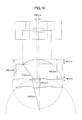
- FIG. 10 is a diagram illustrating an example of a model of a light detection device and its parameters for a ray trace in a first example of a light detection device according to a second embodiment of the present invention.
- Light Tools For the ray trace (a numerical simulation) in a first example of a light detection device according to a second embodiment of the present invention, "Light Tools” was used which is a commercially available lighting design and analysis software.
- an infrared ray sensor which included an infrared ray condensing element and a sensor circuit as illustrated in FIG. 10 .
- An infrared ray condensing element has a first cylindrical face and a second cylindrical face at one side and a third cylindrical face at the other side.
- the first cylindrical face and the second cylindrical face are convex and circular cylindrical faces having identical or common shapes and the third cylindrical face is a concave and circular cylindrical face, A plane including an axis of the first cylindrical face and an axis of the third cylindrical face intersects with a plane including an axis of the second cylindrical face and an axis of the third cylindrical face.
- a distance between an axis of the first cylindrical face and an axis of the third cylindrical face is identical to a distance between an axis of the second cylindrical face and an axis of the third cylindrical face.
- a radius of curvature of the first cylindrical face is identical to a radius of curvature of the second cylindrical face.
- the first cylindrical face and the second cylindrical face have symmetric shapes with respect to a plane which is perpendicular to a plane including an axis of the first cylindrical face and an axis of the second cylindrical face and includes an axis of the third cylindrical face.
- An axis of The first cylindrical face and (an axis of) the second cylindrical face are shifted by a predetermined amount with respect to a plane which is perpendicular to a plane including an axis of the first cylindrical face and an axis of the second cylindrical face and includes an axis of the third cylindrical face.
- parameters of an infrared ray sensor was used which included an infrared ray condensing element and a sensor circuit as illustrated in FIG. 10 .
- Radii of curvature of convex and circular cylindrical faces which were the first cylindrical face and the second cylindrical face were 1200 ⁇ m.
- a radius of curvature of a concave and circular cylindrical face which was the third cylindrical face was 1350 ⁇ m.
- a thickness of an infrared ray condensing element in a direction perpendicular to a plane including an axis of the first cylindrical face and an axis of the second cylindrical face (a distance between a center (or axis) of the first cylindrical face or the second cylindrical face and a perimeter of the third cylindrical face) was 910 ⁇ m.
- a lens thickness of the infrared ray condensing element in a direction perpendicular to a plane including an axis of the first cylindrical face and an axis of the second cylindrical face (a distance between a center (or axis) of the first cylindrical face or a center (or axis) of the second cylindrical face and a center (or axis) of the third cylindrical face) was 850 ⁇ m.
- a lens thickness of the first cylindrical face or the second cylindrical face (a distance between a center (or axis) of the first cylindrical face or the second cylindrical face and a perimeter of the first cylindrical face or the second cylindrical face) was 184 ⁇ m.
- a lens thickness of the third cylindrical face (a distance between a center (or axis) of the third cylindrical face and a perimeter of the third cylindrical face) was 60 ⁇ m.
- a distance between a center (or axis) of the first cylindrical face or a center (or axis) of the second cylindrical face and a center (or axis) of the third cylindrical face (amount of decentering) was 105 ⁇ m.
- FIG. 6 is a diagram illustrating an example of a result of a ray trace in a first example of a light detection device according to a second embodiment of the present invention.
- FIG. 6 An example of a ray trace as illustrated in FIG. 6 is a result of a numerical simulation of the ray trace for an infrared ray condensing element included in an infrared ray sensor as illustrated in FIG. 10 .
- "Light Tools" was used for a numerical simulation of the ray trace for an infrared ray condensing element included in an infrared ray sensor as illustrated in FIG. 10 .
- FIG. 6 illustrates the number of a ray(s) of infrared light condensing on a light receiving surface of a sensor circuit included in an infrared ray sensor versus incident angles of parallel rays of infrared light incident on an infrared ray condensing element included in an infrared ray sensor as illustrated in FIG. 10 .
- a sensor circuit included in an infrared ray sensor has 8 light receiving surfaces (pixels) and a size of each light receiving surface (pixel) is 40 ⁇ m ⁇ 50 ⁇ m.
- FIG. 6 illustrates incident angles (degree(s)) of parallel rays of infrared light incident on an infrared ray condensing element included in an infrared ray sensor as illustrated in FIG. 5 .
- a vertical axis of FIG. 6 illustrates the number of a ray(s) of infrared light condensing on a light receiving surface of a sensor circuit included in an infrared ray sensor.
- a value on a vertical axis of FIG. 6 is a value normalized by the number of a ray(s) of infrared light arriving at a light receiving surface of a sensor circuit included in an infrared ray sensor in a case where there is no infrared ray condensing element.
- a numerical simulation of the ray trace was conducted for only the infrared light ray(s) passing through the first cylindrical face and the third cylindrical face while symmetry for the first cylindrical face and the second cylindrical face was taken into consideration.
- an effect of multiple reflection of an infrared light ray in a circuit board included in an infrared ray sensor and reflection and refraction of an infrared light ray in a cavity structure provided on an infrared ray sensor have been considered.
- FIG. 7 is a diagram illustrating a structure of a second example of a light detection device according to a second embodiment of the present invention.
- An infrared light sensor 700 as a second example of a light detection device according to a second embodiment of the present invention as illustrated in FIG. 7 is a light detection device for detecting infrared light and includes an infrared ray condensing element as an optical element according to a first embodiment of the present invention and a sensor circuit 703 as an element for detecting infrared light condensed by an infrared ray condensing element.
- the sensor circuit 703 is held by a circuit board 704.
- the sensor circuit 703 has plural infrared ray receiving surfaces (pixels) which are arranged one-dimensionally and receive infrared light, and converts infrared light received by an infrared ray receiving surface into an electric signal.
- the infrared light sensor 700 includes a signal amplification circuit for amplifying an electric signal output from the sensor circuit 703 and a signal processing circuit for obtaining information of presence or absence or a direction of a heat source from an output of a signal amplification circuit.
- An infrared ray condensing element included in the infrared light sensor 700 is an optical element for condensing infrared light.
- An infrared ray condensing element condenses infrared light radiated from a heat source onto an infrared ray receiving surface (pixel) of a sensor circuit 703 depending on an incident angle of an infrared light ray.
- An infrared ray condensing element is formed of a transparent semiconductor material for an infrared ray, such as silicon (Si) or germanium (Ge).
- Silicon (Si) is a transparent material for infrared light with a wavelength of about 10 ⁇ m.
- silicon (Si) is preferably used for a transparent material for infrared light.
- silicon (Si) is used for a transparent material for infrared light, not only may it be possible to form an infrared ray condensing element from silicon (Si) but it may also be possible to form the sensor circuit 703, the signal amplification circuit, and the signal processing circuit by using a CMOS process technique.
- An infrared ray condensing element has a first cylindrical face 701a and a second cylindrical face 701b at a side of entrance of an infrared ray and a third cylindrical face 702 at a side of exit of an infrared ray.
- the first cylindrical face 701a and the second cylindrical face 701b are convex and non-circular cylindrical faces and the third cylindrical face 702 is a concave and circular cylindrical face.
- a plane including an axis of the first cylindrical face 701a and an axis of the third cylindrical face 702 intersects with a plane including an axis of the second cylindrical face 701b and an axis of the third cylindrical face 702.
- a distance between an axis of the first cylindrical face 701a and an axis of the third cylindrical face 702 is identical to a distance between an axis of the second cylindrical face 701b and an axis of the third cylindrical face 702.
- a radius of curvature of the first cylindrical face 701a is identical to a radius of curvature of the second cylindrical face 701b.
- the first cylindrical face 701a and the second cylindrical face 701b have mutually symmetric shapes with respect to a plane which is perpendicular to a plane including an axis of the first cylindrical face 701a and an axis of the second cylindrical face 701b and includes an axis of the third cylindrical face 702.
- the first cylindrical face 701a has an asymmetric shape with respect to a plane which is perpendicular to a plane including an axis of the first cylindrical face 701a and an axis of the second cylindrical face 701b and includes an axis of the third cylindrical face 702.
- the first cylindrical face 701a has a face with a relatively high curvature at a left side and has a face with a relatively low curvature at a right side, with respect to a plane which is perpendicular to a plane including an axis of the first cylindrical face 701a and an axis of the second cylindrical face 701b and includes an axis of the third cylindrical face 702.
- the second cylindrical face 701b has an asymmetric shape with respect to a plane which is perpendicular to a plane including an axis of the first cylindrical face 701a and an axis of the second cylindrical face 701b and includes an axis of the third cylindrical face 702.
- the second cylindrical face 701b has a face with a relatively low curvature at a left side and has a face with a relatively high curvature at a right side, with respect to a plane which is perpendicular to a plane including an axis of the first cylindrical face 701a and an axis of the second cylindrical face 701b and includes an axis of the third cylindrical face 702.
- the first cylindrical face 701a and (an axis of) the second cylindrical face 701b are shifted by a predetermined amount Z with respect to a plane which is perpendicular to a plane including an axis of the first cylindrical face 701a and an axis of the second cylindrical face 701b and includes an axis of the third cylindrical face 702.
- a direction of an axis of the first cylindrical face 701a and an axis of the second cylindrical face 701b is a direction orthogonal to a direction of arrangement of one-dimensionally arranged light receiving surfaces (pixels) of the sensor circuit 703.
- the first cylindrical face 701a and the second cylindrical face 701b are mutually shifted in a direction of arrangement of one-dimensionally arranged light receiving surfaces (pixels) of the sensor circuit 703.
- a distance between the third cylindrical face 702 and the sensor circuit 703 is adjusted in such a manner that a size of a spot of infrared light condensed on a light receiving surface of the sensor circuit 703 is reduced.
- the third cylindrical face 702 may have a concave shape engraved on an infrared ray condensing element.
- the first cylindrical face 701a, the second cylindrical face 701b, and the third cylindrical face 702 in an infrared ray condensing element are preferably provided with an anti-reflection coating which is composed of a single layer film or multilayer film which transmits infrared light.
- an anti-reflection coating which is composed of a single layer film or multilayer film which transmits infrared light
- infrared light radiated from a heat source is incident on an infrared ray condensing element in the infrared light sensor 400
- infrared light transmits through the first circular cylindrical face 701a or the second circular cylindrical face 701b and is refracted by the first circular cylindrical face 701a or the second circular cylindrical face 701b correspondingly
- Infrared light having transmitted through the first circular cylindrical face 701a or the second circular cylindrical face 701b is incident on the second circular cylindrical face 702.
- Infrared light having entered the second circular cylindrical face 702 is refracted by the second circular cylindrical face 702 and exits from an infrared ray condensing element.
- Infrared light having exited from an infrared ray condensing element is condensed onto a predetermined light receiving surface (pixel) of the sensor circuit 703 at a relatively short distance.
- a size of the infrared light sensor 700 is often sufficiently small compared to a distance from the infrared light sensor 700 to a heat source, and therefore, it may often be possible to regard infrared light incident on the infrared light sensor 700 as parallel rays of infrared light.
- infrared light incident on the infrared light sensor 700 it may be possible to receive parallel rays of infrared light with two different incident angles on one light receiving surface (pixel) of the sensor circuit 703 included in the infrared light sensor 700, because an infrared ray condensing element has the first cylindrical face 701a and the second cylindrical face 701b.
- the sensor circuit 703 included in the infrared light sensor 700 has N light receiving surfaces (pixels)
- an infrared ray condensing element included in the infrared light sensor 700 As illustrated in FIG. 7 , it may be possible to provide an infrared ray condensing element capable of condensing light with a broader range of incident angles and an infrared light sensor capable of detecting light with a broader range of incident angles, even when the sensor circuit 703 with a relatively few pixel(s) is provided. It may be possible to provide an infrared ray condensing element capable of condensing light at a higher angular resolution and an infrared light sensor capable of detecting light at a higher angular resolution. It may be possible to provide an infrared light sensor capable of obtaining information of presence or absence or a direction of a heat source at a higher precision.
- first cylindrical face 701a and the second cylindrical face 701b of an infrared ray condensing element included in the infrared light sensor 700 as illustrated in FIG. 7 are non-circular cylindrical faces, it may be possible to adjust shapes of non-circular cylindrical faces of the first cylindrical face 701a and the second cylindrical face 701b, and thereby, reduce aberration of infrared light rays condensed on a light receiving surface (pixel) of the sensor circuit 703 included in the infrared ray sensor 700.
- a curvature of field of infrared light rays condensed on a light receiving surface (pixel) of the sensor circuit 703 there is provided, for example, a curvature of field of infrared light rays condensed on a light receiving surface (pixel) of the sensor circuit 703 or the like. It may be possible to provide an infrared ray condensing element capable of condensing light with more reduced aberration and an infrared light sensor capable of detecting light with more reduced aberration. It may be possible to provide an infrared ray condensing element capable of condensing light at a higher resolution and an infrared light sensor capable of detecting light at a higher resolution. It may be possible to provide an infrared light sensor capable of obtaining presence or absence or a direction of a heat source at an even higher precision.
- An infrared ray condensing element further includes a support substrate 705 for supporting a part having the first cylindrical face 701a and the second cylindrical face 701b and the third cylindrical face 702.
- a part having the first cylindrical face 701a and the second cylindrical face 701b and the third cylindrical face 702 is integrated with the support substrate 705.
- the support substrate 705 is bonded to the circuit board 704.
- the circuit board 704 holds the sensor circuit 703, a signal amplification circuit, and a signal processing circuit, and packages the sensor circuit 703, a signal amplification circuit, and a signal processing circuit together with a part having the first cylindrical face 701a and the second cylindrical face 701b and the third cylindrical face 702, and the support substrate 705.
- a length of an infrared ray condensing element in a direction perpendicular to a plane including an axis of the first cylindrical face 701a and an axis of the second cylindrical face 701b, namely, a distance between a straight line on a top of the first cylindrical face 701a or the second cylindrical face 701b and the face bonding circuit board 704 and the support substrate 705, is less than or equal to 1 mm, and therefore, it may be possible to provide a more compact infrared light sensor 700.
- the first cylindrical face 701a, the second cylindrical face 701b, and the third cylindrical face 702 in an infrared ray condensing element included in the infrared light sensor 700 are formed by a molding technique using a mold corresponding to a shape of an infrared ray condensing element.
- the infrared light sensor 700 may be manufactured by a method including forming an infrared ray condensing element from a fist semiconductor wafer, forming the sensor circuit 703, a signal amplification circuit, and a signal processing circuit from a second semiconductor wafer, bonding a first semiconductor wafer with a formed infrared ray condensing element and a second semiconductor wafer with the formed sensor circuit 703, signal amplification circuit, and signal processing circuit, and cutting a bonded first semiconductor wafer and second semiconductor wafer. It may be possible to manufacture the infrared light sensor 700 from a semiconductor wafer by using a semiconductor wafer process.
- the first cylindrical face 701a, the second cylindrical face 701b, and the third cylindrical face 702 in an infrared ray condensing element are formed by using an etching technique for eliminating a portion of a first semiconductor wafer.
- the sensor circuit 703, a signal amplification circuit, and a signal processing circuit are formed by using an etching technique for eliminating a portion of a second semiconductor wafer. It may be possible to manufacture the infrared light sensor 700 with a lower cost and a higher productivity.
- the infrared light sensor 700 may be used as, for example, a motion sensor.
- FIG. 12A and FIG. 12B are diagrams illustrating an example of a model of a light detection device for a ray trace and a result of its ray trace in a fourth example of a light detection device according to a second embodiment of the present invention.
- FIG. 12A is a diagram illustrating a model of a light detection device for a ray trace in a fourth example of a light detection device according to a second embodiment of the present invention.
- a horizontal axis of FIG. 12A represents a horizontal position ( ⁇ m) of an optical element based on an axis of a third cylindrical face of an optical element included in an optical detection device.
- FIG. 12A represents an amount of sag ( ⁇ m) of a first cylindrical face or second cylindrical face of an optical element included in an optical detection device.
- FIG. 12B is a diagram illustrating an example of a result of a ray trace in a fourth example of a light detection device according to a second embodiment of the present invention.
- An example of a model of a light detection device for a ray trace as illustrated in FIG. 12A is similar to an infrared ray sensor including an infrared ray condensing element and a sensor circuit as illustrated in FIG. 10 , except a first cylindrical face and second cylindrical face of an optical element included in a light detection device.
- a first cylindrical face and second cylindrical face of an infrared ray condensing element included in an infrared ray sensor are similar to an example of an optical element according to a first embodiment of the present invention as illustrated in FIG. 11 and have Fresnel lens shapes.
- an infrared ray condensing element included in an infrared ray sensor as illustrated in FIG. 12A amounts of sag of a first cylindrical face and second cylindrical face which have Fresnel lens shapes and are convex faces were 50 ⁇ m.
- a radius of curvature of a third cylindrical face (having a shape of a concave face) of an infrared ray condensing element was 830 ⁇ m.
- a thickness of an infrared ray condensing element was 720 ⁇ m.
- FIG. 12B An example of a ray trace as illustrated in FIG. 12B is a result of a numerical simulation of a ray trace for an infrared ray condensing element included in an infrared ray sensor as illustrated in FIG. 12A .
- "CODE V" was used which is a commercially available optical design / simulation software.
- FIG. 12B illustrates the number of an infrared light ray(s) condensed on a light receiving surface(s) of a sensor circuit included in an infrared ray sensor versus incident angles of parallel rays of infrared light incident on an infrared ray condensing element included in an infrared ray sensor as illustrated in FIG. 12A .
- a horizontal axis of FIG. 12B illustrates incident angles (degrees) of parallel rays of infrared light incident on an infrared ray condensing element included in an infrared ray sensor as illustrated in FIG. 12A .
- FIG. 12B illustrates the number of a ray(s) of infrared light condensed on a light receiving surface of a sensor circuit included in an infrared ray sensor.
- a value on a vertical axis of FIG. 12B is a value normalized by the number of an infrared light ray(s) arriving at a light receiving surface of a sensor circuit included in an infrared ray sensor in a case where there is no infrared ray condensing element.
- FIG. 8A, FIG. 8B, and FIG. 8C are diagrams illustrating a structure of a third example of a light detection device according to a second embodiment of the present invention.
- FIG. 8A is a plan view of a third example of a light detection device according to a second embodiment of the present invention.
- FIG. 8B is a cross-sectional view of a third example of a light detection device according to a second embodiment of the preset invention in direction of AA'.
- FIG. 8C is a cross-sectional view of a third example of a light detection device according to a second embodiment of the present invention in a direction of BB'.
- An infrared light sensor 800 as a third example of a light detection device according to a second embodiment of the present invention as illustrated in FIG. 8A, FIG. 8B, and FIG. 8C is an infrared light device for detecting infrared light and includes an infrared ray condensing element as an optical element according to a first embodiment of the present invention and a sensor circuit 803 as an element for detecting infrared light condensed by an infrared ray condensing element.
- the sensor circuit 803 is held by a circuit board 804.
- the sensor circuit 803 has plural infrared ray receiving surfaces (pixels) which are arranged one-dimensionally and receive infrared light, and converts an infrared light received by an infrared ray receiving surface into an electric signal.
- the infrared light sensor 800 includes a signal amplification circuit for amplifying an electric signal output from the sensor circuit 803 and a signal processing circuit for obtaining information of presence or absence or a direction of a heat source from an output of a signal amplification circuit.
- An infrared ray condensing element included in the infrared light sensor 800 is an optical element for condensing infrared light.
- An infrared ray condensing element condenses infrared light radiated from a heat source onto infrared ray receiving surfaces (pixels) of the sensor circuit 803 depending on an incident angle of an infrared light ray.
- An infrared ray condensing element is formed of a semiconductor material transparent to an infrared ray, such as silicon (Si) or germanium (Ge).
- Silicon (Si) is a material transparent to infrared light with a wavelength of about 10 ⁇ m.
- silicon (Si) is used for a material transparent to infrared light.
- silicon (Si) is used as a material transparent to infrared light, not only may it be possible to form an infrared ray condensing element of silicon (Si) but also it may be possible to form the sensor circuit 803, a signal amplification circuit, and a signal processing circuit by using a CMOS process technique.
- An infrared ray condensing element has a first cylindrical face 801a and a second cylindrical face 801b at a side of entrance of an infrared ray and a third cylindrical face 802 at a side of exit of an infrared ray.
- An infrared ray condensing element has a first plane provided with the first cylindrical face 801a and a second plane provided with the second cylindrical face 801b.
- a first plane and a second plane are planes inclined with respect to a plane including an axis of the first cylindrical face 801a and an axis of the second cylindrical face 801b.
- a first plane and a second plane have symmetric shapes with respect to a plane which is perpendicular to a plane including an axis of the first cylindrical face 801a and an axis of the second cylindrical face 801b and includes an axis of the third cylindrical face 802.
- the first cylindrical face 801a and the second cylindrical face 801b are convex and circular cylindrical faces having identical or common shapes and the third cylindrical face 802 is a concave and circular cylindrical face.
- a plane including an axis of the first cylindrical face 801a and an axis of the third cylindrical face 802 intersects with a plane including an axis of the second cylindrical face 801b and an axis of the third cylindrical face 802.
- a distance between an axis of the first cylindrical face 801a and an axis of the third cylindrical face 802 is identical to a distance between an axis of the second cylindrical face 801b and an axis of the third cylindrical face 802.
- a radius of curvature of the first cylindrical face 801a is identical to a radius of curvature of the second cylindrical face 801b.
- the first cylindrical face 801a and the second cylindrical face 801b have symmetric shapes with respect to a plane which is perpendicular to a plane including an axis of the first cylindrical face 801a and an axis of the second cylindrical face 801b and includes an axis of the third cylindrical face 802.
- a direction of an axis of the first circular cylindrical face 801a and an axis of the second circular cylindrical face 801b is a direction orthogonal to a direction of arrangement of one-dimensionally arranged light receiving surfaces (pixels) of the sensor circuit 803.
- the first cylindrical face 801a and the second cylindrical face 801b are mutually inclined with respect to a light receiving surface (pixel) with respect to one-dimensionally arranged light receiving surfaces (pixels) of the sensor circuit 803.
- a distance between the third cylindrical face 802 and the sensor circuit 803 is adjusted in such a manner that a size of a spot of infrared light condensed on a light receiving surface of the sensor circuit 803 is reduced.
- the third cylindrical face 802 may have a concave shape engraved on an infrared ray condensing element in order to reduce a size of a spot of infrared light condensed on a light receiving surface of the sensor circuit 803.
- the first cylindrical face 801a, the second cylindrical face 801b, and the third cylindrical face 802 in an infrared ray condensing element are preferably provided with an anti-reflection coating which is composed of a single layer film or multilayer film transparent to infrared light.
- an anti-reflection coating which is composed of a single layer film or multilayer film transparent to infrared light
- infrared light radiated from a heat source is incident on an infrared ray condensing element of the infrared light sensor 800
- infrared light transmits through the first circular cylindrical face 801a provided on a first plane or the second circular cylindrical face 801b provided on a second plane and is refracted by the first circular cylindrical face 801a provided on a first plane or the second circular cylindrical face 801b provided on a second plane correspondingly.
- Infrared light having transmitted through the first circular cylindrical face 801a or the second circular cylindrical face 801b is incident on the second circular cylindrical face 802.
- Infrared light entering the second circular cylindrical face 802 is refracted by the second circular cylindrical face 802 and exits from an infrared ray condensing element.
- Infrared light exiting from an infrared ray condensing element condenses on a predetermined light receiving surface (pixel) on the sensor circuit 803 at a relatively short distance.
- a size of the infrared light sensor 800 is often sufficiently small compared to a distance from the infrared light sensor 800 to a heat source, and therefore, it may often be possible to regard infrared light entering the infrared light sensor 800 as parallel rays of infrared light.
- an infrared ray condensing element included in the infrared light sensor 800 When parallel rays of infrared light are incident on an infrared ray condensing element included in the infrared light sensor 800, it may be possible to receive parallel rays of infrared light with two different incident angles on one light receiving surface (pixel) of the sensor circuit 803 included in the infrared light sensor 800, because an infrared ray condensing element has the first cylindrical face 801a provided on a first plane and the second cylindrical face 801b provided on a second plane.
- the sensor circuit 803 included in the infrared light sensor 800 has N light receiving surfaces (pixels)
- an infrared ray condensing element included in the infrared light sensor 800 as illustrated in FIG. 8A, FIG. 8B, and FIG. 8C , it may be possible to provide an infrared ray condensing element capable of condensing light with a broader range of incident angles and an infrared light sensor capable of detecting light with a broader range of incident angles, even when a relatively few pixel(s) of the sensor circuit 803 is/are provided. It may be possible to provide an infrared ray condensing element capable of condensing light at a higher angular resolution and an infrared light sensor capable of detecting light at a higher angular resolution. It may be possible to provide an infrared light sensor capable of obtaining information of presence or absence or a direction of a heat source at a higher precision.
- An infrared ray condensing element further includes a support substrate 805 for supporting a part having the first cylindrical face 801a provided on a first plane and the second cylindrical face 801b provided on a second plane and the third cylindrical face 802.
- a part having the first cylindrical face 801a provided on a first plane and the second cylindrical face 801b provided on a second plane and the third cylindrical face 802 is bonded to the support substrate 805.
- the support substrate 805 is bonded to the circuit board 804.
- the circuit board 804 holds the sensor circuit 803, a signal amplification circuit, and a signal processing circuit, and packages the sensor circuit 803, a signal amplification circuit, and a signal processing circuit together with a part having the first cylindrical face 801a provided on a first plane and the second cylindrical face 801b provided on a second plane and the third cylindrical face 802 and the support substrate 805.
- the first cylindrical face 801a provided on a first plane, the second cylindrical face 801b provided on a second plane, and the third cylindrical face 802, in an infrared ray condensing element included in the infrared light sensor 800, may be formed by a molding technique using a mold corresponding to a shape of an infrared ray condensing element.
- the infrared light sensor 800 may be manufactured by a method including forming an infrared ray condensing element from a first semiconductor wafer, forming the sensor circuit 803, a signal amplification circuit, and a signal processing circuit from a second semiconductor wafer, bonding a first semiconductor wafer with a formed infrared ray condensing element and a second semiconductor wafer with the formed sensor circuit 803, signal amplification circuit, and signal processing circuit, and cutting a bonded first semiconductor wafer and second semiconductor wafer. It may be possible to manufacture the infrared light sensor 800 from a semiconductor wafer by using a semiconductor wafer process.
- the first cylindrical face 801a provided on a first plane, the second cylindrical face 801b provided on a second plane, and the third cylindrical face 802, in an infrared ray condensing element are formed by using an etching technique for eliminating a portion of a first semiconductor wafer.
- the sensor circuit 803, a signal amplification circuit, and a signal processing element are formed by using an etching technique for eliminating a portion of a second semiconductor wafer. It may be possible to manufacture the infrared light sensor 800 with a lower cost and a higher productivity.
- the infrared light sensor 800 may be used as, for example, a motion sensor.
- FIG. 13 is a diagram illustrating a general structure of an object sensing system according to a third embodiment of the present invention.
- An object sensing system 1300 includes a light detection device for detecting light from an object and a device for sensing existence or displacement of an object based on light detected by a light detection device.
- An object is, for example, a heat source 1301 for emitting at least an infrared ray.
- a light detection device is an infrared ray sensor 1302 as a light detection device according to a second embodiment of the present invention.
- the infrared ray sensor 1302 includes an infrared ray condensing element and a sensor circuit.
- An infrared ray condensing element has a first cylindrical face and a second cylindrical face at one side and a third cylindrical face at the other side.
- an infrared ray emitted from the heat source 1301 is condensed on a sensor circuit of the infrared ray sensor 1302 by an infrared ray condensing element of the infrared ray sensor 1302.
- An angle of view of the infrared ray sensor 1302 is a sum of an angle of view ⁇ 1 of a first cylindrical face of an infrared ray condensing element and an angle of view ⁇ 2 of a second cylindrical face of an infrared ray condensing element.
- an infrared ray emitted from the heat source 1301 passes through the first cylindrical face and the third cylindrical face of an infrared ray condensing element and is condensed by a sensor circuit.
- an infrared ray emitted from the heat source 1301 passes through the second cylindrical face and the third cylindrical face of an infrared ray condensing element and is condensed on a sensor circuit.
- An infrared ray condensed by a sensor circuit is converted into N bit data for parallel output or time series data for serial output by a sensor circuit.
- N bit data for parallel output or time series data for serial output as obtained by a sensor circuit are output to a signal processing device 1303 connected to the infrared ray sensor 1302.
- the signal processing device 1303 determines information of existence (presence or absence) or displacement of the heat source 1301 as an object in an angle of view of the infrared ray sensor 1302 based on data output from the infrared ray sensor 1302.
- the signal processing device 1303 there is provided, for example, a signal amplification processing device, a differential processing device, a noise elimination processing device, a threshold determination device, or the like.
- Information determined by the signal processing device 1303 is transmitted to a controlled apparatus 1304 connected to the signal processing device 1303 and controlled by the signal processing device 1303, as, for example, flag output or temperature data. Data transmitted from the signal processing device 1303 to the controlled apparatus 1304 determine operation of the controlled apparatus 1304.
- controlled apparatus 1304 which is controlled by the signal processing device 1303, there is provided, for example, a home electric appliance such as a personal computer, a television set, or an air conditioner, an office instrument, or an alarm for security application, or the like.
- a home electric appliance such as a personal computer, a television set, or an air conditioner, an office instrument, or an alarm for security application, or the like.
- the controlled apparatus 1304 is utilized, for example, for the purpose of energy management such as electric power saving or raising of caution for a person.
- an object sensing system capable of sensing existence or displacement of an object based on light with a broader range of incident angles.
- An optical element according to a first embodiment of the present invention, a light detection device according to a second embodiment of the present invention, and an object sensing system according to a third embodiment of the present invention are an optical element for condensing light or an electromagnetic wave(s), a light detection device for detecting light or an electromagnetic wave(s), and an object sensing system based on light or an electromagnetic wave(s), respectively.
- An optical element according to a first embodiment of the present invention, a light detection device according to a second embodiment of the present invention, and an object sensing system according to a third embodiment of the present invention are not limited to an optical element for condensing an infrared light or an infrared ray, a light detection device for detecting infrared light or an infrared ray, and an object sensing system based on infrared light or an infrared ray, respectively.
- an optical element for condensing light or an electromagnetic wave(s) from an object a light detection device for detecting light or an electromagnetic wave(s) from an object, and an object sensing system based on light or an electromagnetic wave(s) from an object by selecting a material transmitting light or an electric wave(s) from an object.
Landscapes
- Physics & Mathematics (AREA)
- General Physics & Mathematics (AREA)
- Optics & Photonics (AREA)
- Spectroscopy & Molecular Physics (AREA)
- Health & Medical Sciences (AREA)
- Toxicology (AREA)
- Photometry And Measurement Of Optical Pulse Characteristics (AREA)
- Geophysics And Detection Of Objects (AREA)
- Lenses (AREA)
Applications Claiming Priority (2)
| Application Number | Priority Date | Filing Date | Title |
|---|---|---|---|
| JP2011061629 | 2011-03-18 | ||
| JP2012015594A JP6111517B2 (ja) | 2011-03-18 | 2012-01-27 | 光学素子及び光検出デバイス並びに物体検知システム |
Publications (2)
| Publication Number | Publication Date |
|---|---|
| EP2500752A1 true EP2500752A1 (de) | 2012-09-19 |
| EP2500752B1 EP2500752B1 (de) | 2022-09-14 |
Family
ID=46027556
Family Applications (1)
| Application Number | Title | Priority Date | Filing Date |
|---|---|---|---|
| EP12159779.3A Active EP2500752B1 (de) | 2011-03-18 | 2012-03-16 | Optisches Element, Lichterkennungsvorrichtung, und Objekterkennungssystem |
Country Status (3)
| Country | Link |
|---|---|
| US (1) | US8895910B2 (de) |
| EP (1) | EP2500752B1 (de) |
| JP (1) | JP6111517B2 (de) |
Families Citing this family (9)
| Publication number | Priority date | Publication date | Assignee | Title |
|---|---|---|---|---|
| JP2015133594A (ja) | 2014-01-10 | 2015-07-23 | 株式会社リコー | 撮像モジュール及び撮像装置 |
| JP6572559B2 (ja) | 2014-03-12 | 2019-09-11 | 株式会社リコー | 光変調素子、撮像装置及び画像投影装置 |
| US10018341B2 (en) * | 2014-07-31 | 2018-07-10 | JST Performance, LLC | Method and apparatus for a light collection and projection system |
| JP6390864B2 (ja) * | 2015-12-04 | 2018-09-19 | パナソニックIpマネジメント株式会社 | 照明装置およびそれを用いた走行体 |
| US9863596B2 (en) * | 2016-01-29 | 2018-01-09 | Chun-Te Wu | Optical element, optical module, and lens carrier |
| US10326038B2 (en) * | 2017-11-02 | 2019-06-18 | Lawrence Livermore National Security, Llc | Three-dimensional co-axial linear photonic switch |
| KR102253239B1 (ko) * | 2019-10-16 | 2021-05-17 | 이준섭 | 원적외선 열화상 센서 어셈블리용 윈도우 및 이를 포함하는 원적외선 열화상 센서 어셈블리 |
| CN115077727B (zh) * | 2021-03-15 | 2024-04-26 | 四川大学 | 一种在线检测透明元件前后表面面形的方法 |
| JP2024052098A (ja) | 2022-09-30 | 2024-04-11 | 株式会社リコー | 網膜投影表示装置、頭部装着型表示装置および検眼装置 |
Citations (9)
| Publication number | Priority date | Publication date | Assignee | Title |
|---|---|---|---|---|
| US4740701A (en) * | 1985-05-24 | 1988-04-26 | Cerberus Ag | Infrared intrusion detector |
| GB2207523A (en) * | 1987-07-27 | 1989-02-01 | Philips Electronic Associated | Lens arrays in two planes |
| US5107120A (en) * | 1989-09-22 | 1992-04-21 | Pennwalt Corporation | Passive infrared detector |
| US20070152156A1 (en) * | 2005-03-21 | 2007-07-05 | Visonic Ltd. | Passive infra-red detectors |
| US20080112057A1 (en) * | 2006-11-09 | 2008-05-15 | Takashi Ono | Optical device and crystallization device |
| JP2008128913A (ja) | 2006-11-22 | 2008-06-05 | Matsushita Electric Works Ltd | 赤外線検出装置 |
| JP2008166234A (ja) * | 2007-01-05 | 2008-07-17 | Stanley Electric Co Ltd | 面照明装置 |
| JP2011061629A (ja) | 2009-09-11 | 2011-03-24 | Ricoh Co Ltd | 検出回路 |
| JP2012015594A (ja) | 2010-06-29 | 2012-01-19 | Nippon Soken Inc | 超音波センサ |
Family Cites Families (5)
| Publication number | Priority date | Publication date | Assignee | Title |
|---|---|---|---|---|
| US4322124A (en) * | 1980-05-05 | 1982-03-30 | Honeywell Inc. | Low cost wide field of view infrared sensor |
| GB2213927A (en) * | 1987-12-18 | 1989-08-23 | Philips Electronic Associated | Pyroelectric infrared sensors |
| JP2621430B2 (ja) * | 1988-10-21 | 1997-06-18 | 松下電器産業株式会社 | 光センサー |
| JP2501596Y2 (ja) * | 1990-04-27 | 1996-06-19 | 松下電工株式会社 | 熱線式検知器 |
| JP2010170081A (ja) * | 2008-12-25 | 2010-08-05 | Tokuyama Corp | 遠赤外線用光学素子 |
-
2012
- 2012-01-27 JP JP2012015594A patent/JP6111517B2/ja active Active
- 2012-03-15 US US13/421,281 patent/US8895910B2/en active Active
- 2012-03-16 EP EP12159779.3A patent/EP2500752B1/de active Active
Patent Citations (9)
| Publication number | Priority date | Publication date | Assignee | Title |
|---|---|---|---|---|
| US4740701A (en) * | 1985-05-24 | 1988-04-26 | Cerberus Ag | Infrared intrusion detector |
| GB2207523A (en) * | 1987-07-27 | 1989-02-01 | Philips Electronic Associated | Lens arrays in two planes |
| US5107120A (en) * | 1989-09-22 | 1992-04-21 | Pennwalt Corporation | Passive infrared detector |
| US20070152156A1 (en) * | 2005-03-21 | 2007-07-05 | Visonic Ltd. | Passive infra-red detectors |
| US20080112057A1 (en) * | 2006-11-09 | 2008-05-15 | Takashi Ono | Optical device and crystallization device |
| JP2008128913A (ja) | 2006-11-22 | 2008-06-05 | Matsushita Electric Works Ltd | 赤外線検出装置 |
| JP2008166234A (ja) * | 2007-01-05 | 2008-07-17 | Stanley Electric Co Ltd | 面照明装置 |
| JP2011061629A (ja) | 2009-09-11 | 2011-03-24 | Ricoh Co Ltd | 検出回路 |
| JP2012015594A (ja) | 2010-06-29 | 2012-01-19 | Nippon Soken Inc | 超音波センサ |
Also Published As
| Publication number | Publication date |
|---|---|
| JP2012212108A (ja) | 2012-11-01 |
| EP2500752B1 (de) | 2022-09-14 |
| US20120235027A1 (en) | 2012-09-20 |
| JP6111517B2 (ja) | 2017-04-12 |
| US8895910B2 (en) | 2014-11-25 |
Similar Documents
| Publication | Publication Date | Title |
|---|---|---|
| EP2500752B1 (de) | Optisches Element, Lichterkennungsvorrichtung, und Objekterkennungssystem | |
| TWI480598B (zh) | 光學式偵測裝置及使用其之機器設備 | |
| US8913119B2 (en) | Short distance iris recognition camera | |
| CN102183222B (zh) | 螺旋输送系统同轴度和平面度动态定量测量方法及装置 | |
| KR20150084656A (ko) | 정보 처리 장치 및 방법 | |
| KR101109834B1 (ko) | 감지 모듈과 이를 구비한 광학 감지 시스템 | |
| CN1657869A (zh) | 位置测量系统及用于位置测量的透镜 | |
| US8969784B2 (en) | Optical lens assembly and optical devices thereof | |
| CN101807131B (zh) | 侦测模块及包含此侦测模块的光学侦测系统 | |
| US20180025204A1 (en) | Optical fingerprint sensor with prism module | |
| KR102103767B1 (ko) | 가스 센서용 광 공동 및 그를 이용한 가스센서 | |
| JP2013200367A (ja) | フレネルレンズおよび光学検出器 | |
| KR20140042633A (ko) | 적외선센서모듈 | |
| US20150276490A1 (en) | Sensor assembly | |
| US9772718B2 (en) | Optical touch device and touch detecting method using the same | |
| US9922233B1 (en) | Thin type optical fingerprint sensor | |
| US20100321558A1 (en) | Apparatus and method for detecting spatial movement of object | |
| CN104570342B (zh) | 一种检测设备光学系统的设计方法 | |
| WO2018072604A1 (zh) | 智能镜 | |
| CN207200710U (zh) | 用于近距离无线光通信系统中的集成自聚焦光电接收单元 | |
| US10042084B2 (en) | Reflective type PIR motion detection system | |
| KR101752955B1 (ko) | 차량공조시스템 제어용 적외선 센서의 제작방법 | |
| CN102829859A (zh) | 光学测量系统及其装置 | |
| CN210775894U (zh) | 一种雨量感应器本体及其构成的集成式传感器 | |
| US20220291357A1 (en) | Optical sensing system |
Legal Events
| Date | Code | Title | Description |
|---|---|---|---|
| PUAI | Public reference made under article 153(3) epc to a published international application that has entered the european phase |
Free format text: ORIGINAL CODE: 0009012 |
|
| 17P | Request for examination filed |
Effective date: 20120316 |
|
| AK | Designated contracting states |
Kind code of ref document: A1 Designated state(s): AL AT BE BG CH CY CZ DE DK EE ES FI FR GB GR HR HU IE IS IT LI LT LU LV MC MK MT NL NO PL PT RO RS SE SI SK SM TR |
|
| AX | Request for extension of the european patent |
Extension state: BA ME |
|
| STAA | Information on the status of an ep patent application or granted ep patent |
Free format text: STATUS: EXAMINATION IS IN PROGRESS |
|
| 17Q | First examination report despatched |
Effective date: 20180213 |
|
| GRAP | Despatch of communication of intention to grant a patent |
Free format text: ORIGINAL CODE: EPIDOSNIGR1 |
|
| STAA | Information on the status of an ep patent application or granted ep patent |
Free format text: STATUS: GRANT OF PATENT IS INTENDED |
|
| INTG | Intention to grant announced |
Effective date: 20220407 |
|
| RIN1 | Information on inventor provided before grant (corrected) |
Inventor name: SAKAI, ATSUSHI Inventor name: SANGU, SUGURU |
|
| GRAS | Grant fee paid |
Free format text: ORIGINAL CODE: EPIDOSNIGR3 |
|
| GRAA | (expected) grant |
Free format text: ORIGINAL CODE: 0009210 |
|
| STAA | Information on the status of an ep patent application or granted ep patent |
Free format text: STATUS: THE PATENT HAS BEEN GRANTED |
|
| AK | Designated contracting states |
Kind code of ref document: B1 Designated state(s): AL AT BE BG CH CY CZ DE DK EE ES FI FR GB GR HR HU IE IS IT LI LT LU LV MC MK MT NL NO PL PT RO RS SE SI SK SM TR |
|
| REG | Reference to a national code |
Ref country code: GB Ref legal event code: FG4D |
|
| RIN1 | Information on inventor provided before grant (corrected) |
Inventor name: SAKAI, ATSUSHI Inventor name: SANGU, SUGURU |
|
| REG | Reference to a national code |
Ref country code: CH Ref legal event code: EP |
|
| REG | Reference to a national code |
Ref country code: DE Ref legal event code: R096 Ref document number: 602012078742 Country of ref document: DE |
|
| REG | Reference to a national code |
Ref country code: IE Ref legal event code: FG4D |
|
| REG | Reference to a national code |
Ref country code: AT Ref legal event code: REF Ref document number: 1519039 Country of ref document: AT Kind code of ref document: T Effective date: 20221015 |
|
| REG | Reference to a national code |
Ref country code: LT Ref legal event code: MG9D |
|
| REG | Reference to a national code |
Ref country code: NL Ref legal event code: MP Effective date: 20220914 |
|
| PG25 | Lapsed in a contracting state [announced via postgrant information from national office to epo] |
Ref country code: SE Free format text: LAPSE BECAUSE OF FAILURE TO SUBMIT A TRANSLATION OF THE DESCRIPTION OR TO PAY THE FEE WITHIN THE PRESCRIBED TIME-LIMIT Effective date: 20220914 Ref country code: RS Free format text: LAPSE BECAUSE OF FAILURE TO SUBMIT A TRANSLATION OF THE DESCRIPTION OR TO PAY THE FEE WITHIN THE PRESCRIBED TIME-LIMIT Effective date: 20220914 Ref country code: NO Free format text: LAPSE BECAUSE OF FAILURE TO SUBMIT A TRANSLATION OF THE DESCRIPTION OR TO PAY THE FEE WITHIN THE PRESCRIBED TIME-LIMIT Effective date: 20221214 Ref country code: LV Free format text: LAPSE BECAUSE OF FAILURE TO SUBMIT A TRANSLATION OF THE DESCRIPTION OR TO PAY THE FEE WITHIN THE PRESCRIBED TIME-LIMIT Effective date: 20220914 Ref country code: LT Free format text: LAPSE BECAUSE OF FAILURE TO SUBMIT A TRANSLATION OF THE DESCRIPTION OR TO PAY THE FEE WITHIN THE PRESCRIBED TIME-LIMIT Effective date: 20220914 Ref country code: FI Free format text: LAPSE BECAUSE OF FAILURE TO SUBMIT A TRANSLATION OF THE DESCRIPTION OR TO PAY THE FEE WITHIN THE PRESCRIBED TIME-LIMIT Effective date: 20220914 |
|
| REG | Reference to a national code |
Ref country code: AT Ref legal event code: MK05 Ref document number: 1519039 Country of ref document: AT Kind code of ref document: T Effective date: 20220914 |
|
| PG25 | Lapsed in a contracting state [announced via postgrant information from national office to epo] |
Ref country code: HR Free format text: LAPSE BECAUSE OF FAILURE TO SUBMIT A TRANSLATION OF THE DESCRIPTION OR TO PAY THE FEE WITHIN THE PRESCRIBED TIME-LIMIT Effective date: 20220914 Ref country code: GR Free format text: LAPSE BECAUSE OF FAILURE TO SUBMIT A TRANSLATION OF THE DESCRIPTION OR TO PAY THE FEE WITHIN THE PRESCRIBED TIME-LIMIT Effective date: 20221215 |
|
| PG25 | Lapsed in a contracting state [announced via postgrant information from national office to epo] |
Ref country code: SM Free format text: LAPSE BECAUSE OF FAILURE TO SUBMIT A TRANSLATION OF THE DESCRIPTION OR TO PAY THE FEE WITHIN THE PRESCRIBED TIME-LIMIT Effective date: 20220914 Ref country code: RO Free format text: LAPSE BECAUSE OF FAILURE TO SUBMIT A TRANSLATION OF THE DESCRIPTION OR TO PAY THE FEE WITHIN THE PRESCRIBED TIME-LIMIT Effective date: 20220914 Ref country code: PT Free format text: LAPSE BECAUSE OF FAILURE TO SUBMIT A TRANSLATION OF THE DESCRIPTION OR TO PAY THE FEE WITHIN THE PRESCRIBED TIME-LIMIT Effective date: 20230116 Ref country code: ES Free format text: LAPSE BECAUSE OF FAILURE TO SUBMIT A TRANSLATION OF THE DESCRIPTION OR TO PAY THE FEE WITHIN THE PRESCRIBED TIME-LIMIT Effective date: 20220914 Ref country code: CZ Free format text: LAPSE BECAUSE OF FAILURE TO SUBMIT A TRANSLATION OF THE DESCRIPTION OR TO PAY THE FEE WITHIN THE PRESCRIBED TIME-LIMIT Effective date: 20220914 Ref country code: AT Free format text: LAPSE BECAUSE OF FAILURE TO SUBMIT A TRANSLATION OF THE DESCRIPTION OR TO PAY THE FEE WITHIN THE PRESCRIBED TIME-LIMIT Effective date: 20220914 |
|
| PG25 | Lapsed in a contracting state [announced via postgrant information from national office to epo] |
Ref country code: SK Free format text: LAPSE BECAUSE OF FAILURE TO SUBMIT A TRANSLATION OF THE DESCRIPTION OR TO PAY THE FEE WITHIN THE PRESCRIBED TIME-LIMIT Effective date: 20220914 Ref country code: PL Free format text: LAPSE BECAUSE OF FAILURE TO SUBMIT A TRANSLATION OF THE DESCRIPTION OR TO PAY THE FEE WITHIN THE PRESCRIBED TIME-LIMIT Effective date: 20220914 Ref country code: IS Free format text: LAPSE BECAUSE OF FAILURE TO SUBMIT A TRANSLATION OF THE DESCRIPTION OR TO PAY THE FEE WITHIN THE PRESCRIBED TIME-LIMIT Effective date: 20230114 Ref country code: EE Free format text: LAPSE BECAUSE OF FAILURE TO SUBMIT A TRANSLATION OF THE DESCRIPTION OR TO PAY THE FEE WITHIN THE PRESCRIBED TIME-LIMIT Effective date: 20220914 |
|
| REG | Reference to a national code |
Ref country code: DE Ref legal event code: R097 Ref document number: 602012078742 Country of ref document: DE |
|
| PG25 | Lapsed in a contracting state [announced via postgrant information from national office to epo] |
Ref country code: NL Free format text: LAPSE BECAUSE OF FAILURE TO SUBMIT A TRANSLATION OF THE DESCRIPTION OR TO PAY THE FEE WITHIN THE PRESCRIBED TIME-LIMIT Effective date: 20220914 Ref country code: AL Free format text: LAPSE BECAUSE OF FAILURE TO SUBMIT A TRANSLATION OF THE DESCRIPTION OR TO PAY THE FEE WITHIN THE PRESCRIBED TIME-LIMIT Effective date: 20220914 |
|
| P01 | Opt-out of the competence of the unified patent court (upc) registered |
Effective date: 20230525 |
|
| PLBE | No opposition filed within time limit |
Free format text: ORIGINAL CODE: 0009261 |
|
| STAA | Information on the status of an ep patent application or granted ep patent |
Free format text: STATUS: NO OPPOSITION FILED WITHIN TIME LIMIT |
|
| PG25 | Lapsed in a contracting state [announced via postgrant information from national office to epo] |
Ref country code: DK Free format text: LAPSE BECAUSE OF FAILURE TO SUBMIT A TRANSLATION OF THE DESCRIPTION OR TO PAY THE FEE WITHIN THE PRESCRIBED TIME-LIMIT Effective date: 20220914 |
|
| 26N | No opposition filed |
Effective date: 20230615 |
|
| PG25 | Lapsed in a contracting state [announced via postgrant information from national office to epo] |
Ref country code: SI Free format text: LAPSE BECAUSE OF FAILURE TO SUBMIT A TRANSLATION OF THE DESCRIPTION OR TO PAY THE FEE WITHIN THE PRESCRIBED TIME-LIMIT Effective date: 20220914 |
|
| PG25 | Lapsed in a contracting state [announced via postgrant information from national office to epo] |
Ref country code: MC Free format text: LAPSE BECAUSE OF FAILURE TO SUBMIT A TRANSLATION OF THE DESCRIPTION OR TO PAY THE FEE WITHIN THE PRESCRIBED TIME-LIMIT Effective date: 20220914 |
|
| REG | Reference to a national code |
Ref country code: CH Ref legal event code: PL |
|
| REG | Reference to a national code |
Ref country code: BE Ref legal event code: MM Effective date: 20230331 |
|
| PG25 | Lapsed in a contracting state [announced via postgrant information from national office to epo] |
Ref country code: LU Free format text: LAPSE BECAUSE OF NON-PAYMENT OF DUE FEES Effective date: 20230316 |
|
| REG | Reference to a national code |
Ref country code: IE Ref legal event code: MM4A |
|
| PG25 | Lapsed in a contracting state [announced via postgrant information from national office to epo] |
Ref country code: LI Free format text: LAPSE BECAUSE OF NON-PAYMENT OF DUE FEES Effective date: 20230331 Ref country code: IE Free format text: LAPSE BECAUSE OF NON-PAYMENT OF DUE FEES Effective date: 20230316 Ref country code: CH Free format text: LAPSE BECAUSE OF NON-PAYMENT OF DUE FEES Effective date: 20230331 |
|
| PG25 | Lapsed in a contracting state [announced via postgrant information from national office to epo] |
Ref country code: BE Free format text: LAPSE BECAUSE OF NON-PAYMENT OF DUE FEES Effective date: 20230331 |
|
| PG25 | Lapsed in a contracting state [announced via postgrant information from national office to epo] |
Ref country code: IT Free format text: LAPSE BECAUSE OF FAILURE TO SUBMIT A TRANSLATION OF THE DESCRIPTION OR TO PAY THE FEE WITHIN THE PRESCRIBED TIME-LIMIT Effective date: 20220914 |
|
| PG25 | Lapsed in a contracting state [announced via postgrant information from national office to epo] |
Ref country code: BG Free format text: LAPSE BECAUSE OF FAILURE TO SUBMIT A TRANSLATION OF THE DESCRIPTION OR TO PAY THE FEE WITHIN THE PRESCRIBED TIME-LIMIT Effective date: 20220914 |
|
| PG25 | Lapsed in a contracting state [announced via postgrant information from national office to epo] |
Ref country code: BG Free format text: LAPSE BECAUSE OF FAILURE TO SUBMIT A TRANSLATION OF THE DESCRIPTION OR TO PAY THE FEE WITHIN THE PRESCRIBED TIME-LIMIT Effective date: 20220914 |
|
| PGFP | Annual fee paid to national office [announced via postgrant information from national office to epo] |
Ref country code: DE Payment date: 20250319 Year of fee payment: 14 |
|
| PGFP | Annual fee paid to national office [announced via postgrant information from national office to epo] |
Ref country code: FR Payment date: 20250325 Year of fee payment: 14 |
|
| PGFP | Annual fee paid to national office [announced via postgrant information from national office to epo] |
Ref country code: GB Payment date: 20250321 Year of fee payment: 14 |
|
| PG25 | Lapsed in a contracting state [announced via postgrant information from national office to epo] |
Ref country code: CY Free format text: LAPSE BECAUSE OF FAILURE TO SUBMIT A TRANSLATION OF THE DESCRIPTION OR TO PAY THE FEE WITHIN THE PRESCRIBED TIME-LIMIT; INVALID AB INITIO Effective date: 20120316 |
|
| PG25 | Lapsed in a contracting state [announced via postgrant information from national office to epo] |
Ref country code: HU Free format text: LAPSE BECAUSE OF FAILURE TO SUBMIT A TRANSLATION OF THE DESCRIPTION OR TO PAY THE FEE WITHIN THE PRESCRIBED TIME-LIMIT; INVALID AB INITIO Effective date: 20120316 |
|
| PG25 | Lapsed in a contracting state [announced via postgrant information from national office to epo] |
Ref country code: TR Free format text: LAPSE BECAUSE OF FAILURE TO SUBMIT A TRANSLATION OF THE DESCRIPTION OR TO PAY THE FEE WITHIN THE PRESCRIBED TIME-LIMIT Effective date: 20220914 |