EP2499731B1 - Power system having voltage-based monitoring for over current protection - Google Patents
Power system having voltage-based monitoring for over current protection Download PDFInfo
- Publication number
- EP2499731B1 EP2499731B1 EP10775998.7A EP10775998A EP2499731B1 EP 2499731 B1 EP2499731 B1 EP 2499731B1 EP 10775998 A EP10775998 A EP 10775998A EP 2499731 B1 EP2499731 B1 EP 2499731B1
- Authority
- EP
- European Patent Office
- Prior art keywords
- power
- power supply
- voltage
- link
- output
- Prior art date
- Legal status (The legal status is an assumption and is not a legal conclusion. Google has not performed a legal analysis and makes no representation as to the accuracy of the status listed.)
- Active
Links
Images


Classifications
-
- H—ELECTRICITY
- H02—GENERATION; CONVERSION OR DISTRIBUTION OF ELECTRIC POWER
- H02M—APPARATUS FOR CONVERSION BETWEEN AC AND AC, BETWEEN AC AND DC, OR BETWEEN DC AND DC, AND FOR USE WITH MAINS OR SIMILAR POWER SUPPLY SYSTEMS; CONVERSION OF DC OR AC INPUT POWER INTO SURGE OUTPUT POWER; CONTROL OR REGULATION THEREOF
- H02M1/00—Details of apparatus for conversion
- H02M1/42—Circuits or arrangements for compensating for or adjusting power factor in converters or inverters
- H02M1/4208—Arrangements for improving power factor of AC input
- H02M1/4225—Arrangements for improving power factor of AC input using a non-isolated boost converter
-
- H—ELECTRICITY
- H02—GENERATION; CONVERSION OR DISTRIBUTION OF ELECTRIC POWER
- H02M—APPARATUS FOR CONVERSION BETWEEN AC AND AC, BETWEEN AC AND DC, OR BETWEEN DC AND DC, AND FOR USE WITH MAINS OR SIMILAR POWER SUPPLY SYSTEMS; CONVERSION OF DC OR AC INPUT POWER INTO SURGE OUTPUT POWER; CONTROL OR REGULATION THEREOF
- H02M1/00—Details of apparatus for conversion
- H02M1/32—Means for protecting converters other than automatic disconnection
-
- H—ELECTRICITY
- H02—GENERATION; CONVERSION OR DISTRIBUTION OF ELECTRIC POWER
- H02M—APPARATUS FOR CONVERSION BETWEEN AC AND AC, BETWEEN AC AND DC, OR BETWEEN DC AND DC, AND FOR USE WITH MAINS OR SIMILAR POWER SUPPLY SYSTEMS; CONVERSION OF DC OR AC INPUT POWER INTO SURGE OUTPUT POWER; CONTROL OR REGULATION THEREOF
- H02M1/00—Details of apparatus for conversion
- H02M1/0067—Converter structures employing plural converter units, other than for parallel operation of the units on a single load
- H02M1/007—Plural converter units in cascade
-
- Y—GENERAL TAGGING OF NEW TECHNOLOGICAL DEVELOPMENTS; GENERAL TAGGING OF CROSS-SECTIONAL TECHNOLOGIES SPANNING OVER SEVERAL SECTIONS OF THE IPC; TECHNICAL SUBJECTS COVERED BY FORMER USPC CROSS-REFERENCE ART COLLECTIONS [XRACs] AND DIGESTS
- Y02—TECHNOLOGIES OR APPLICATIONS FOR MITIGATION OR ADAPTATION AGAINST CLIMATE CHANGE
- Y02B—CLIMATE CHANGE MITIGATION TECHNOLOGIES RELATED TO BUILDINGS, e.g. HOUSING, HOUSE APPLIANCES OR RELATED END-USER APPLICATIONS
- Y02B70/00—Technologies for an efficient end-user side electric power management and consumption
- Y02B70/10—Technologies improving the efficiency by using switched-mode power supplies [SMPS], i.e. efficient power electronics conversion e.g. power factor correction or reduction of losses in power supplies or efficient standby modes
Definitions
- the present invention relates in general to the field of electronics, and more specifically to a power control system and method with voltage-based monitoring for over current protection.
- Power control systems often utilize one or more power conversion stages to convert alternating current (AC) voltages to direct current (DC) voltages or perform DC-to-DC conversions.
- power control systems often contain a power factor correction (PFC) stage to provide power factor correction and regulate a link voltage, an output stage to provide output power to a load, and an isolation stage to isolate the PFC stage from the output stage.
- PFC power factor correction
- the PFC stage and the output stage of a power control system have a one hundred percent (100%) rated power and a maximum power.
- the rated power refers to power available from the power control system under nominal operation conditions.
- the maximum power refers to a percentage of the rated power that can be supplied by the power control system for at least a limited period of time while maintaining a regulated output voltage and without damaging the power control systems and/or the load.
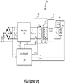
- FIG. 1 depicts a power control system 100, and power control system 100 includes a PFC stage 102, an output stage 104, and an isolation stage 106 to isolate the PFC stage 102 from the output stage 104.
- Voltage source 108 supplies an alternating current (AC) input voltage V IN to a full bridge diode rectifier 110.
- Capacitor 112 provides high frequency filtering.
- the voltage source 108 is, for example, a public utility, and the AC voltage V IN is, for example, a 60 Hz/110 V line voltage in the United States of America or a 50 Hz/220 V line voltage in Europe.
- the rectifier 110 rectifies the input voltage V IN and supplies a rectified, time-varying, line input voltage V X to the PFC stage 102.
- the power control system 100 includes a controller 114 to regulate a link voltage V LINK of PFC stage 102 and control isolation stage 106. Controller 114 generates a pulse-width modulated control signal CS 0 to control power factor correction and regulate the link voltage V LINK of PFC stage 102.
- PFC stage 102 is a boost-type, switching power converter
- control signal CS 0 is a switch control signal that controls conversion of input voltage V X to link voltage V LINK .
- Controller 114 monitors voltages V X and V LINK to generate switch control signal CS 0 .
- Isolation stage 106 isolates the PFC stage 102 from the output stage 104.
- the link voltage V LINK is either a multiple or a fraction of the input voltage V X .
- the load 116 may not be compatible with the value of the link voltage V LINK or compatible with a DC voltage in general.
- Isolation stage 106 includes a transformer 118 to convert the link voltage V LINK into the output voltage V OUT .
- Transformer 118 is a flyback type transformer that includes switch 124.
- Control signal CS F controls the conductivity of switch 124 to convert link voltage V LINK into a time-varying, primary-side voltage Vp to allow the primary-side windings 120 of transformer 118 to alternately store energy and then transfer energy to the secondary-side windings 122.
- switch 124 is a field effect transistor (FET).
- Transformer 118 converts the primary side voltage Vp into a secondary voltage V S .
- FET field effect transistor
- the output stage 104 converts the secondary voltage Vs into the output voltage V OUT .
- the topology of output stage 104 is a matter of design choice. Exemplary topologies are a half-bridge buck converter and a full-bridge buck converter. Examples of output stage 104 are also discussed in chapter 6 of Fundamentals of Power Electronics.
- Power control system 100 supplies load 116 with output voltage V OUT and output current i OUT .
- the load 116 is any device that can utilize the power provided by output stage 104.
- Controller 114 regulates the link voltage V LINK and the primary-side voltage V p to establish a particular value for the secondary-side load current i OUT .
- Controller 114 regulates the primary-side voltage V p by controlling the duty cycles of control signal CS F .
- Controller 114 obtains a value of the output current I OUT by sensing a feedback voltage V R SENSE across sense resistor 126.
- the output current I OUT equals V R _ SENSE /R, and R is the known resistance of sense resistor 126.
- Controller 114 regulates link voltage V LINK and the primary-side V p based on the value of output current i OUT . If the value of the output current i OUT is too large, controller 114 decreases the duty cycle of control signal CS F to reduce the value of output current i OUT . If the value of secondary side current i OUT is too small, controller 114 increases the duty cycle of control signal CS F to increase the value output current i OUT .
- PFC stage 102 has a rated power of P RATED and a maximum power of P MAX . If load 116 demands more power than the maximum power P MAX , the output current I OUT increases and the output voltage V OUT decreases. If the output current I OUT exceeds a predetermined threshold value, the power control system 100 enters an over current protection mode.
- the particular over current protection mode involves, for example, turning the power control system 100 OFF to protect components of the power control system 100 from damage.
- WO 2006 013557 describes a system for supplying power to a load and for controlling the power factor presented to the power line. Output voltage is controlled by a digital, outer, control loop, and inner, analog, control loop causes the input current to be substantially proportional to the input voltage at any particular point in the power line cycle. Thus, the system presents a load to the power line that appears to be purely resistive.
- One aspect of the invention provides an apparatus according to claim 1.
- a corresponding method is also provided.
- a power control system reduces power losses while monitoring for an over current event by utilizing an over current protection method that detects the over current event based on an output voltage of an output stage of the power control system and power utilization information.
- the power utilization information represents power utilization of a power supply of the power control system.
- the power utilization of the power supply is represented as a normalized, power utilization factor.
- the power control system detects the over current event by sensing only voltages and, in at least one embodiment, without sensing an output current in an output stage of the power control system. Since the output current is not sensed, the power control system avoids power losses otherwise associated with sensing the output current.
- the power control system includes the power factor correction (PFC) stage to provide power factor correction and, in at least one embodiment, to regulate an output voltage of the PFC stage.
- the power control system also includes an isolation stage to isolate the PFC stage from the output stage while allowing the PFC stage to transfer energy to the output stage.
- the power control system also includes a controller to control the PFC stage and the isolation stage.
- the controller includes an over current protection module ("OCP module").
- OCP module determines the power utilization factor P UTIL using voltages sensed from the PFC stage and/or the isolation stage.
- the OCP module responds to the over current event by entering an over current protection mode.
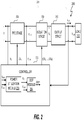
- Figure 2 depicts a power control system 200 that includes a power supply and a controller 202.
- the controller 202 provides over current protection and controls conversion of an input voltage V X into an output voltage V OUT .
- controller 202 includes a power utilization module 203 that determines power utilization information in the form of a power utilization factor P UTIL .
- the power utilization factor P UTIL is a normalized value ranging from 0-1.
- the power utilization factor P UTIL represents the power demanded of power control system 200 by load 212.
- the power utilization factor P UTIL is expressed as a normalized percentage of the rated power P RATED (as defined below) of power control system 200. For example, when the power utilization factor P UTIL is 0, the power demand of load 212 is zero. When the power utilization factor P UTIL is 1, the power demand of load 212 is 100% of rated power P RATED .
- the OCP module 204 determines the power utilization factor P UTIL using the link voltage V LINK and a reference voltage V REF .
- the OCP module 204 utilizes the output voltage V OUT of output stage 210 of power supply 201 and the power utilization factor P UTIL to determine when to enter an over current protection mode to, for example, protect power control system 200 from an over current event.
- an over current event refers to an increase in the output current i OUT above a predetermined output current threshold I OUT_TH .
- the OCP module 204 does not utilize sensed currents to protect the power control system 200 from an over current event, and, thus, avoids power losses associated with current sensing.
- the rated power P RATED of power control system 200 represents an amount of power that power supply 201 can nominally supply to load 212.
- a rated power P RATED of 100W indicates that the power supply 201 can nominally supply load 212 with up to 100W of power.
- Power supply 201 also has a maximum power P MAX .
- the maximum power P MAX is generally a percentage increase of, for example 25%, over the rated power P RATED .
- a maximum power P MAX is 125% of the rated power P RATED , which equals 125W.
- the maximum power P MAX represents an amount of power that power supply 201 can supply to load 212 while maintaining an approximately constant output voltage V OUT .
- Power control system 200 maintains an approximately constant output voltage V OUT if the power demand of load 212 is less than or equal to the maximum power P MAX of power supply 201. If load 212 begins to demand more power from power supply 201 than the maximum power P MAX , then P equals P MAX in Equation [1], output current i OUT will increase in proportion to the power demand increase, and the output voltage V OUT will decrease in accordance with Equation [1]. In at least one embodiment, when power utilization factor P UTIL equals 1 (indicating that the power control system is generating 100% of rated power) and the output voltage V OUT decreases to a predetermined threshold voltage V OUT_TH .
- the threshold voltage V OUT_TH is set to correspond with a maximum allowable output current I OUT , as described below.
- the OCP module 204 generates an output signal OCP indicating entry into over current protection mode.
- the particular operation(s) associated with the over current protection mode is a matter of design choice.
- controller 202 turns PFC stage 206 OFF. In another embodiment, controller 202 turns PFC stage 206 OFF and, then, restarts PFC stage 206.
- the PFC stage 206 receives the input voltage V X .
- the input voltage V X is a rectified alternating current (AC) voltage, such as a rectified 60 Hz/110 V line voltage in the United States of America or a rectified 50 Hz/220 V line voltage in Europe.
- AC alternating current
- the particular topology of the PFC stage 206 is a matter of design choice.
- PFC stage 206 can be a switching type boost, buck, buck-boost, or C ⁇ k converter.
- the PFC stage 206 generates a link voltage V LINK .
- the link voltage V LINK is a regulated, approximately DC voltage.
- the power supply 201 also includes an isolation stage 208 that isolates the PFC stage 206 from an output stage 210 and converts the link voltage V LINK into a secondary voltage V S .
- the particular topology of the isolation stage 208 is a matter of design choice.
- the isolation stage 208 can be a transformer based isolation stage such as a flyback, full bridge, or half bridge transformer.
- the output stage 210 receives the secondary voltage V S and provides an output voltage V OUT and an output current I OUT to load 212.
- the particular topology of the output stage 210 is also a matter of design choice.
- output stage 210 can have a flyback topology.
- the load 212 can be any load for which power control system 200 can provide power. Examples of load 212 include lamps, such as light emitting diode and gas discharge type lamps, cellular telephones, personal computer (PCs) computing devices including personal digital assistants, and other electronic devices.
- isolation stage 208 and output stage 210 are separate and distinct as shown in Figure 2 . In at least one embodiment, isolation stage 208 and output stage 210 are combined into a single circuit. For example, in at least one embodiment, isolation stage 208 and output stage 210 are configured together as a single, flyback converter.
- controller 202 In addition to providing over current protection, controller 202 generates a control signal CS 1 for PFC stage 206 to control power factor correction of PFC stage 206 and, in at least one embodiment, to also regulate the link voltage V LINK to a particular value.
- U.S. Patent Application No. 11/967269 entitled “POWER CONTROL SYSTEM USING A NONLINEAR DELTA-SIGMA MODULATOR WITH NONLINEAR POWER CONVERSION PROCESS MODELING", filed December 31, 2007, inventor John L. Melanson, and assignee Cirrus Logic, Inc. (referred to herein as "Melanson I”) describes exemplary generation of control signal, such as control signal CS 1 , and control of PFC stage implemented as a switching power converter.
- Controller 202 also generates control signals CS 2 through CS N to control isolation stage 208, and N is an integer index and is greater than or equal to 2.
- Melanson I describes exemplary generation of control signals CS 2 through CS N .
- controller 202 can be implemented as one or more physically distinct circuits.
- controller 202 is a single integrated circuit.
- controller 202 is implemented as two embodiments with one embodiment controlling PFC stage 206 and one embodiment controlling isolation stage 208.
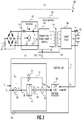
- FIG. 3 depicts power control system 300, which represents one embodiment of power control system 200.
- Power control system 300 includes a power supply 301, and power supply 301 includes a PFC stage 302, an output stage 304, and an isolation stage 306 to isolate the PFC stage 302 from the output stage 304.
- Voltage source 308 supplies an alternating current (AC) input voltage V IN to a full bridge diode rectifier 310.
- Capacitor 312 provides high frequency filtering.
- the voltage source 308 is, for example, a public utility, and the AC voltage V IN is, for example, a 60 Hz/110 V line voltage in the United States of America or a 50 Hz/220 V line voltage in Europe.
- the rectifier 310 rectifies the input voltage V in and supplies a rectified, time-varying, line input voltage V X to the PFC stage 302.
- the power control system 300 includes a controller 314 to regulate a link voltage V LINK of PFC stage 302 and control isolation stage 306. Controller 314 also protects power control system 300 when load 332 is demanding more than the rated power P RATED of power supply 301 and the output voltage decreases below a predetermined threshold value V OUT_TH . Controller 314 generates a pulse-width modulated switch control signal CS 1 to control power factor correction and regulate the link voltage V LINK of PFC stage 302.
- PFC stage 302 is a boost-type, switching power converter, and switch control signal CS 1 is a switch control signal that controls switch 316.
- switch control signal CS 1 is a duty cycle modulated signal
- switch 316 is a field effect transistor (FET).
- Controller 314 monitors voltages V X and V LINK to generate switch control signal CS 1 .
- controller 314 generates switch control signal CS 1 as described in Melanson I.
- the PFC stage 302 includes an inductor 318 that conducts a current i L .
- inductor current i L energizes inductor 318.
- switch 316 is OFF, diode 320 is forward biased, and inductor current i L charges link capacitor 322.
- the link voltage V LINK across link capacitor 322 remains approximately constant during operation of PFC stage 302.
- Controller 314 operates PFC stage 302 in discontinuous conduction mode (DCM). In DCM, the inductor current i L decreases to zero while switch 316 is OFF and remains at zero for a finite time before switch 316 turns ON.
- DCM discontinuous conduction mode
- Isolation stage 306 isolates the PFC stage 302 from the output stage 304 and converts the DC link voltage V LINK into an AC voltage so that transformer 328 can transfer energy from link capacitor 322 via the primary side windings 324 to the secondary-side windings 326 of transformer 328.
- Isolation stage 306 also includes a primary-side transformer interface 330.
- the primary-side transformer interface 330 can be any type of interface. In at least one embodiment, primary-side transformer interface 330 is a half-bridge interface as described in U.S. Patent Application No. 12/415,830 , entitled "PRIMARY-SIDE BASED CONTROL OF SECONDARY-SIDE CURRENT FOR A TRANSFORMER," inventor John L. Melanson, Attorney Docket No.
- Control signals CS 2 through CS N control isolation stage 306, and N is an integer index that is greater than or equal to 2.
- a variety of other topologies are well-known for isolation stage 306, such as full-bridge topologies as discussed in chapter 6 of Fundamentals of Power Electronics.
- the output stage 304 converts the secondary voltage V S into the output voltage V OUT .
- the topology of output stage 304 is a matter of design choice.
- the output stage 304 is a half-bridge, buck converter as described in Melanson II.
- Other exemplary topologies, such as a full-bridge buck converter, are also discussed in chapter 6 of Fundamentals of Power Electronics.
- Power supply 301 supplies load 332 with output voltage V OUT and output current i OUT .
- Controller 314 regulates the link voltage V LINK and the primary-side voltage Vp to establish a particular value for the secondary-side load current i OUT .
- Controller 314 includes a power utilization module ("P UTIL module") 333 which represents one embodiment of power utilization module 203.
- the P UTIL module 333 generates the power utilization factor P UTIL .
- the power utilization factor P UTIL varies as the difference between the reference voltage V REF and the link voltage V LINK , as represented by error signal e v from error generator 336 varies.
- the link voltage V LINK varies in proportion to the power demand by load 332.
- the power utilization factor P UTIL also varies in proportion to power demand by load 332.
- the power utilization factor P UTIL is a normalized representation of the power demand of load 332.
- the reference voltage V REF is set to a desired value of the link voltage V LINK .
- the desired value of link voltage V LINK is 100V, so the reference voltage V REF is set to 100 V.
- the P UTIL module 333 includes an integral signal path 338 and a proportional signal path 340.
- the integral signal path 338 includes an integrator 342 to integrate the error signal e v and also includes a gain module 344 to multiply the integral of error signal e v by a gain factor g2 and generate the integrated output signal I PW .
- the proportional path 340 includes a gain module 346 to multiply the error signal e v by a gain factor g1 and generate the proportional output signal P PW .
- Adder 348 adds the integrated output signal I PW and the proportional output signal P PW to generate the power utilization factor P UTIL .
- the values of gain factors g1 and g2 are a matter of design choice.
- the gain factors g1 and g2 affect the responsiveness of OCP module 314 in tracking changes in power demand by load 332.
- Exemplary values of gain factors g1 and g2 are set forth in the emulation code of Figures 8-31 in Melanson I. Additionally, in at least one embodiment, the link voltage V LINK , the reference voltage V REF , and the output voltage V OUT monitored by the P UTIL module 333 are scaled versions of the actual voltages.
- Controller 314 also includes OCP module 334 to detect an over current event in power supply 301.
- the OCP module 334 also provides an over current protection signal OCP that causes power control system 300 to enter an over current protection mode.
- over current protection signal OCP causes power control system 300 to enter an over current protection mode when power supply 301 is operating above 100% rated power P RATED .
- Figure 4 depicts an exemplary over current protection algorithm 400.
- the OCP module 314 determines whether to cause power control system 300 to enter over current protection mode in accordance with the over current protection algorithm 400.
- the P UTIL module 333 monitors the link voltage V LINK , and in operation 404, power utilization factor P UTIL is determined.
- OCP mode module 334 monitors the output voltage V OUT .
- the OCP module 334 stores a power utilization factor threshold P UTIL TH .
- the power utilization factor threshold P UTIL TH is set to a value that indicates the power demand of load 332 is at or close to 100% of the rated power P RATED of power supply 301.
- the power utilization factor threshold P UTIL TH is set to a value that reflects a margin of error in the determination of the power utilization factor P UTIL .
- power utilization factor threshold P UTIL TH is 0.95, which reflects a margin of error of 5% in the determination of power utilization factor P UTIL .
- the OCP mode module 334 determines whether the power utilization factor P UTIL is greater than the power utilization factor threshold P UTIL TH . If power utilization factor P UTIL is less than the power utilization factor threshold P UTIL TH , then load 332 is not demanding more than 100% of the rated power P RATED of power supply 301. OCP module 334 then returns to operation 402 and continues therefrom. If the power utilization factor P UTIL is greater than the power utilization factor threshold P UTIL TH , then load 332 is demanding more power than the power corresponding to the power utilization factor threshold P UTIL TH .
- OCP module 334 determines whether the output voltage V OUT is less than the threshold voltage V OUT _ TH .
- Figure 5 depicts an exemplary over current protection graph 500, which depicts the relationship between the output voltage V OUT ( Figure 3 ), the output current i OUT , and entry into over current protection mode by power control system 300. Referring to Figures 3 , 4 , and 5 . If the power demand of load 332 exceeds the maximum power P MAX of power supply 301, the output current I OUT will increase and the output voltage V OUT will decrease in accordance with Equation [1]. In at least one embodiment, the threshold voltage V OUT_TH is set to correspond with a maximum allowable output current i OUT .
- the threshold voltage V OUT_TH is set to 10V.
- operation 410 determines that the output voltage V OUT is greater than the threshold voltage V OUT _ TH , then: (1) from operation 408, load 332 is demanding more power than the maximum power P MAX of power supply 301 and (2) the output current I OUT exceeds the maximum allowable output current i OUT_TH .
- OCP mode module 334 To protect power control system 300 from an output current i OUT exceeding the maximum allowable output current i OUT_TH , in operation 412, OCP mode module 334 generates the OCP signal indicating an over current protection event, and controller 3 14 enters over current protection mode.
- the particular over current protection mode is a design choice. In at least one embodiment, in over current protection mode, controller 3 14 turns PFC stage 302 OFF. In another embodiment, controller 3 14 turns PFC stage 302 OFF and, then, restarts PFC stage 206.
- a power control system can provide overcurrent protection using sensed voltages without incurring current sensing power losses.
Landscapes
- Engineering & Computer Science (AREA)
- Power Engineering (AREA)
- Dc-Dc Converters (AREA)
- Rectifiers (AREA)
Description
- The present invention relates in general to the field of electronics, and more specifically to a power control system and method with voltage-based monitoring for over current protection.
- Power control systems often utilize one or more power conversion stages to convert alternating current (AC) voltages to direct current (DC) voltages or perform DC-to-DC conversions. For example, power control systems often contain a power factor correction (PFC) stage to provide power factor correction and regulate a link voltage, an output stage to provide output power to a load, and an isolation stage to isolate the PFC stage from the output stage.
- The PFC stage and the output stage of a power control system have a one hundred percent (100%) rated power and a maximum power. The rated power refers to power available from the power control system under nominal operation conditions. The maximum power refers to a percentage of the rated power that can be supplied by the power control system for at least a limited period of time while maintaining a regulated output voltage and without damaging the power control systems and/or the load. Once the load begins demanding more power than the maximum power of the power control system, an output current of the output stage will increase, and an output voltage of the output stage will decrease. A controller that controls the power control system monitors the output current. When the output current exceeds a predetermined threshold, the controller will enter an overcurrent protection mode. However, circuitry used to sense the current can cause overall power losses and, thus, lower the efficiency of the power control system.
-
Figure 1 depicts apower control system 100, andpower control system 100 includes aPFC stage 102, anoutput stage 104, and anisolation stage 106 to isolate thePFC stage 102 from theoutput stage 104.Voltage source 108 supplies an alternating current (AC) input voltage VIN to a fullbridge diode rectifier 110. Capacitor 112 provides high frequency filtering. Thevoltage source 108 is, for example, a public utility, and the AC voltage VIN is, for example, a 60 Hz/110 V line voltage in the United States of America or a 50 Hz/220 V line voltage in Europe. Therectifier 110 rectifies the input voltage VIN and supplies a rectified, time-varying, line input voltage VX to thePFC stage 102. - The
power control system 100 includes acontroller 114 to regulate a link voltage VLINK ofPFC stage 102 andcontrol isolation stage 106.Controller 114 generates a pulse-width modulated control signal CS0 to control power factor correction and regulate the link voltage VLINK ofPFC stage 102. In one embodiment,PFC stage 102 is a boost-type, switching power converter, and control signal CS0 is a switch control signal that controls conversion of input voltage VX to link voltage VLINK. Controller 114 monitors voltages VX and VLINK to generate switch control signal CS0. -
Isolation stage 106 isolates thePFC stage 102 from theoutput stage 104. Depending upon the type ofPFC stage 102, the link voltage VLINK is either a multiple or a fraction of the input voltage VX. In either situation, theload 116 may not be compatible with the value of the link voltage VLINK or compatible with a DC voltage in general.Isolation stage 106 includes atransformer 118 to convert the link voltage VLINK into the output voltage VOUT. Transformer 118 is a flyback type transformer that includesswitch 124. Control signal CSF controls the conductivity ofswitch 124 to convert link voltage VLINK into a time-varying, primary-side voltage Vp to allow the primary-side windings 120 oftransformer 118 to alternately store energy and then transfer energy to the secondary-side windings 122. In one embodiment,switch 124 is a field effect transistor (FET).Transformer 118 converts the primary side voltage Vp into a secondary voltage VS. A variety of other topologies are well-known forisolation stage 106, such as half-bridge and full-bridge topologies as discussed in chapter 6 of Fundamentals of Power Electronics - Second Edition by Erickson and Maksimović, publisher Springer Science+Business Media, LLC, copyright 2001 ("Fundamentals of Power Electronics"). - The
output stage 104 converts the secondary voltage Vs into the output voltage VOUT. The topology ofoutput stage 104 is a matter of design choice. Exemplary topologies are a half-bridge buck converter and a full-bridge buck converter. Examples ofoutput stage 104 are also discussed in chapter 6 of Fundamentals of Power Electronics. -
Power control system 100supplies load 116 with output voltage VOUT and output current iOUT. Theload 116 is any device that can utilize the power provided byoutput stage 104.Controller 114 regulates the link voltage VLINK and the primary-side voltage Vp to establish a particular value for the secondary-side load current iOUT.Controller 114 regulates the primary-side voltage Vp by controlling the duty cycles of control signal CSF.Controller 114 obtains a value of the output current IOUT by sensing a feedback voltage VR SENSE acrosssense resistor 126. The output current IOUT equals VR_SENSE/R, and R is the known resistance ofsense resistor 126.Controller 114 regulates link voltage VLINK and the primary-side Vp based on the value of output current iOUT. If the value of the output current iOUT is too large,controller 114 decreases the duty cycle of control signal CSF to reduce the value of output current iOUT. If the value of secondary side current iOUT is too small,controller 114 increases the duty cycle of control signal CSF to increase the value output current iOUT. -
PFC stage 102 has a rated power of PRATED and a maximum power of PMAX. Ifload 116 demands more power than the maximum power PMAX, the output current IOUT increases and the output voltage VOUT decreases. If the output current IOUT exceeds a predetermined threshold value, thepower control system 100 enters an over current protection mode. The particular over current protection mode involves, for example, turning thepower control system 100 OFF to protect components of thepower control system 100 from damage. - Power efficiency is generally a concern when designing and utilizing
power control system 100. However, the voltage drop corresponding to the feedback voltage VR_SENSE acrosssense resistor 126 represents a power loss. Such power loss is disadvantageous.WO 2006 013557 describes a system for supplying power to a load and for controlling the power factor presented to the power line. Output voltage is controlled by a digital, outer, control loop, and inner, analog, control loop causes the input current to be substantially proportional to the input voltage at any particular point in the power line cycle. Thus, the system presents a load to the power line that appears to be purely resistive. - One aspect of the invention provides an apparatus according to claim 1.
- A corresponding method is also provided.
- Preferred embodiments are addressed in the dependent claims.
- The present invention may be better understood, and its numerous objects, features and advantages made apparent to those skilled in the art by referencing the accompanying drawings. The use of the same reference number throughout the several figures designates a like or similar element.
-
Figure 1 (labeled prior art) depicts a power control system that monitors for an over current event by sensing an output stage current across a sense resistor. -
Figure 2 depicts a power control system that monitors for an over current event using a power utilization factor and an output stage voltage. -
Figure 3 depicts an embodiment of the power control system ofFigure 2 . -
Figure 4 depicts an over current protection algorithm. -
Figure 5 depicts an over current protection graph. - A power control system reduces power losses while monitoring for an over current event by utilizing an over current protection method that detects the over current event based on an output voltage of an output stage of the power control system and power utilization information. The power utilization information represents power utilization of a power supply of the power control system. In at least one embodiment, the power utilization of the power supply is represented as a normalized, power utilization factor. In at least one embodiment, the power control system detects the over current event by sensing only voltages and, in at least one embodiment, without sensing an output current in an output stage of the power control system. Since the output current is not sensed, the power control system avoids power losses otherwise associated with sensing the output current.
- In at least one embodiment, addition to the output stage, the power control system includes the power factor correction (PFC) stage to provide power factor correction and, in at least one embodiment, to regulate an output voltage of the PFC stage. The power control system also includes an isolation stage to isolate the PFC stage from the output stage while allowing the PFC stage to transfer energy to the output stage. In at least one embodiment, the power control system also includes a controller to control the PFC stage and the isolation stage. The controller includes an over current protection module ("OCP module"). In at least one embodiment, the OCP module determines the power utilization factor PUTIL using voltages sensed from the PFC stage and/or the isolation stage. In at least one embodiment, the OCP module responds to the over current event by entering an over current protection mode.
-
Figure 2 depicts apower control system 200 that includes a power supply and acontroller 202. Thecontroller 202 provides over current protection and controls conversion of an input voltage VX into an output voltage VOUT. In at least one embodiment,controller 202 includes apower utilization module 203 that determines power utilization information in the form of a power utilization factor PUTIL. In at least one embodiment, the power utilization factor PUTIL is a normalized value ranging from 0-1. The power utilization factor PUTIL represents the power demanded ofpower control system 200 byload 212. In at least one embodiment, the power utilization factor PUTIL is expressed as a normalized percentage of the rated power PRATED (as defined below) ofpower control system 200. For example, when the power utilization factor PUTIL is 0, the power demand ofload 212 is zero. When the power utilization factor PUTIL is 1, the power demand ofload 212 is 100% of rated power PRATED. - In at least one embodiment, the
OCP module 204 determines the power utilization factor PUTIL using the link voltage VLINK and a reference voltage VREF. TheOCP module 204 utilizes the output voltage VOUT ofoutput stage 210 ofpower supply 201 and the power utilization factor PUTIL to determine when to enter an over current protection mode to, for example, protectpower control system 200 from an over current event. In at least one embodiment, an over current event refers to an increase in the output current iOUT above a predetermined output current threshold IOUT_TH. In at least one embodiment, theOCP module 204 does not utilize sensed currents to protect thepower control system 200 from an over current event, and, thus, avoids power losses associated with current sensing. - As subsequently described in more detail, the rated power PRATED of
power control system 200 represents an amount of power thatpower supply 201 can nominally supply to load 212. For example, a rated power PRATED of 100W indicates that thepower supply 201 can nominally supplyload 212 with up to 100W of power.Power supply 201 also has a maximum power PMAX. The maximum power PMAX is generally a percentage increase of, for example 25%, over the rated power PRATED. Thus, in at least one embodiment, for a rated power PRATED of 100W and a 25% increase, a maximum power PMAX is 125% of the rated power PRATED, which equals 125W. The maximum power PMAX represents an amount of power thatpower supply 201 can supply to load 212 while maintaining an approximately constant output voltage VOUT. Equation [1] represents an exemplary relationship between the output power P ofpower supply 201, the output current iOUT, and the output voltage VOUT:
power supply 201, VOUT represents the output voltage ofoutput stage 210, and iOUT represents the output current ofoutput stage 210. -
Power control system 200 maintains an approximately constant output voltage VOUT if the power demand ofload 212 is less than or equal to the maximum power PMAX ofpower supply 201. Ifload 212 begins to demand more power frompower supply 201 than the maximum power PMAX, then P equals PMAX in Equation [1], output current iOUT will increase in proportion to the power demand increase, and the output voltage VOUT will decrease in accordance with Equation [1]. In at least one embodiment, when power utilization factor PUTIL equals 1 (indicating that the power control system is generating 100% of rated power) and the output voltage VOUT decreases to a predetermined threshold voltage VOUT_TH. In at least one embodiment, the threshold voltage VOUT_TH is set to correspond with a maximum allowable output current IOUT, as described below. TheOCP module 204 generates an output signal OCP indicating entry into over current protection mode. The particular operation(s) associated with the over current protection mode is a matter of design choice. In at least one embodiment, in over current protection mode,controller 202 turnsPFC stage 206 OFF. In another embodiment,controller 202 turnsPFC stage 206 OFF and, then, restartsPFC stage 206. - For the
power control system 200 to convert the input voltage VX into the output voltage VOUT, thePFC stage 206 receives the input voltage VX. In at least one embodiment, the input voltage VX is a rectified alternating current (AC) voltage, such as a rectified 60 Hz/110 V line voltage in the United States of America or a rectified 50 Hz/220 V line voltage in Europe. The particular topology of thePFC stage 206 is a matter of design choice. For example,PFC stage 206 can be a switching type boost, buck, buck-boost, or Cúk converter. ThePFC stage 206 generates a link voltage VLINK. In at least one embodiment, the link voltage VLINK is a regulated, approximately DC voltage. - The
power supply 201 also includes anisolation stage 208 that isolates thePFC stage 206 from anoutput stage 210 and converts the link voltage VLINK into a secondary voltage VS. The particular topology of theisolation stage 208 is a matter of design choice. For example, theisolation stage 208 can be a transformer based isolation stage such as a flyback, full bridge, or half bridge transformer. - The
output stage 210 receives the secondary voltage VS and provides an output voltage VOUT and an output current IOUT to load 212. The particular topology of theoutput stage 210 is also a matter of design choice. For example,output stage 210 can have a flyback topology. Theload 212 can be any load for whichpower control system 200 can provide power. Examples ofload 212 include lamps, such as light emitting diode and gas discharge type lamps, cellular telephones, personal computer (PCs) computing devices including personal digital assistants, and other electronic devices. Additionally, in at least one embodiment,isolation stage 208 andoutput stage 210 are separate and distinct as shown inFigure 2 . In at least one embodiment,isolation stage 208 andoutput stage 210 are combined into a single circuit. For example, in at least one embodiment,isolation stage 208 andoutput stage 210 are configured together as a single, flyback converter. - In addition to providing over current protection,
controller 202 generates a control signal CS1 forPFC stage 206 to control power factor correction ofPFC stage 206 and, in at least one embodiment, to also regulate the link voltage VLINK to a particular value.U.S. Patent Application No. 11/967269 Controller 202 also generates control signals CS2 through CSN to controlisolation stage 208, and N is an integer index and is greater than or equal to 2. Melanson I describes exemplary generation of control signals CS2 through CSN. In at least one embodiment,controller 202 can be implemented as one or more physically distinct circuits. For example, in at least one embodiment,controller 202 is a single integrated circuit. In at least one embodiment,controller 202 is implemented as two embodiments with one embodiment controllingPFC stage 206 and one embodiment controllingisolation stage 208. -
Figure 3 depictspower control system 300, which represents one embodiment ofpower control system 200.Power control system 300 includes apower supply 301, andpower supply 301 includes aPFC stage 302, anoutput stage 304, and anisolation stage 306 to isolate thePFC stage 302 from theoutput stage 304.Voltage source 308 supplies an alternating current (AC) input voltage VIN to a fullbridge diode rectifier 310.Capacitor 312 provides high frequency filtering. Thevoltage source 308 is, for example, a public utility, and the AC voltage VIN is, for example, a 60 Hz/110 V line voltage in the United States of America or a 50 Hz/220 V line voltage in Europe. Therectifier 310 rectifies the input voltage Vin and supplies a rectified, time-varying, line input voltage VX to thePFC stage 302. - The
power control system 300 includes acontroller 314 to regulate a link voltage VLINK ofPFC stage 302 and controlisolation stage 306.Controller 314 also protectspower control system 300 whenload 332 is demanding more than the rated power PRATED ofpower supply 301 and the output voltage decreases below a predetermined threshold value VOUT_TH. Controller 314 generates a pulse-width modulated switch control signal CS1 to control power factor correction and regulate the link voltage VLINK ofPFC stage 302.PFC stage 302 is a boost-type, switching power converter, and switch control signal CS1 is a switch control signal that controlsswitch 316. In at least one embodiment, switch control signal CS1, is a duty cycle modulated signal, and switch 316 is a field effect transistor (FET).Controller 314 monitors voltages VX and VLINK to generate switch control signal CS1. In at least one embodiment,controller 314 generates switch control signal CS1 as described in Melanson I. - The
PFC stage 302 includes aninductor 318 that conducts a current iL. Whenswitch 316 is ON,diode 320 is reverse biased, and inductor current iL energizesinductor 318. Whenswitch 316 is OFF,diode 320 is forward biased, and inductor current iL charges linkcapacitor 322. The link voltage VLINK acrosslink capacitor 322 remains approximately constant during operation ofPFC stage 302.Controller 314 operatesPFC stage 302 in discontinuous conduction mode (DCM). In DCM, the inductor current iL decreases to zero whileswitch 316 is OFF and remains at zero for a finite time beforeswitch 316 turns ON. -
Isolation stage 306 isolates thePFC stage 302 from theoutput stage 304 and converts the DC link voltage VLINK into an AC voltage so thattransformer 328 can transfer energy fromlink capacitor 322 via theprimary side windings 324 to the secondary-side windings 326 oftransformer 328.Isolation stage 306 also includes a primary-side transformer interface 330. The primary-side transformer interface 330 can be any type of interface. In at least one embodiment, primary-side transformer interface 330 is a half-bridge interface as described inU.S. Patent Application No. 12/415,830 control isolation stage 306, and N is an integer index that is greater than or equal to 2. A variety of other topologies are well-known forisolation stage 306, such as full-bridge topologies as discussed in chapter 6 of Fundamentals of Power Electronics. - The
output stage 304 converts the secondary voltage VS into the output voltage VOUT. The topology ofoutput stage 304 is a matter of design choice. In at least one embodiment, theoutput stage 304 is a half-bridge, buck converter as described in Melanson II. Other exemplary topologies, such as a full-bridge buck converter, are also discussed in chapter 6 of Fundamentals of Power Electronics. -
Power supply 301 supplies load 332 with output voltage VOUT and output current iOUT.Controller 314 regulates the link voltage VLINK and the primary-side voltage Vp to establish a particular value for the secondary-side load current iOUT.Controller 314 includes a power utilization module ("PUTIL module") 333 which represents one embodiment ofpower utilization module 203. The PUTIL module 333 generates the power utilization factor PUTIL. The power utilization factor PUTIL varies as the difference between the reference voltage VREF and the link voltage VLINK, as represented by error signal e v fromerror generator 336 varies. The link voltage VLINK varies in proportion to the power demand byload 332. Accordingly, the power utilization factor PUTIL also varies in proportion to power demand byload 332. As previously described, the power utilization factor PUTIL is a normalized representation of the power demand ofload 332. In at least one embodiment, the reference voltage VREF is set to a desired value of the link voltage VLINK. For example, in at least one embodiment, the desired value of link voltage VLINK is 100V, so the reference voltage VREF is set to 100 V. The PUTIL module 333 includes anintegral signal path 338 and aproportional signal path 340. - The
integral signal path 338 includes anintegrator 342 to integrate the error signal ev and also includes again module 344 to multiply the integral of error signal ev by a gain factor g2 and generate the integrated output signal IPW. Theproportional path 340 includes again module 346 to multiply the error signal ev by a gain factor g1 and generate the proportional output signal PPW. Adder 348 adds the integrated output signal IPW and the proportional output signal PPW to generate the power utilization factor PUTIL. The values of gain factors g1 and g2 are a matter of design choice. The gain factors g1 and g2 affect the responsiveness ofOCP module 314 in tracking changes in power demand byload 332. Exemplary values of gain factors g1 and g2 are set forth in the emulation code of Figures 8-31 in Melanson I. Additionally, in at least one embodiment, the link voltage VLINK, the reference voltage VREF, and the output voltage VOUT monitored by the PUTIL module 333 are scaled versions of the actual voltages. -
Controller 314 also includesOCP module 334 to detect an over current event inpower supply 301. TheOCP module 334 also provides an over current protection signal OCP that causespower control system 300 to enter an over current protection mode. In at least one embodiment, over current protection signal OCP causespower control system 300 to enter an over current protection mode whenpower supply 301 is operating above 100% rated power PRATED. -
Figure 4 depicts an exemplary overcurrent protection algorithm 400. Referring toFigures 3 and4 , in at least one embodiment, theOCP module 314 determines whether to causepower control system 300 to enter over current protection mode in accordance with the overcurrent protection algorithm 400. Inoperation 402, the PUTIL module 333 monitors the link voltage VLINK, and inoperation 404, power utilization factor PUTIL is determined. - In
operation 406,OCP mode module 334 monitors the output voltage VOUT. TheOCP module 334 stores a power utilization factor threshold PUTIL TH. In at least one embodiment, the power utilization factor threshold PUTIL TH is set to a value that indicates the power demand ofload 332 is at or close to 100% of the rated power PRATED ofpower supply 301. In at least one embodiment, the power utilization factor threshold PUTIL TH is set to a value that reflects a margin of error in the determination of the power utilization factor PUTIL. For example, in at least one embodiment, power utilization factor threshold PUTIL TH is 0.95, which reflects a margin of error of 5% in the determination of power utilization factor PUTIL. - In
operation 408, theOCP mode module 334 determines whether the power utilization factor PUTIL is greater than the power utilization factor threshold PUTIL TH. If power utilization factor PUTIL is less than the power utilization factor threshold PUTIL TH, then load 332 is not demanding more than 100% of the rated power PRATED ofpower supply 301.OCP module 334 then returns tooperation 402 and continues therefrom. If the power utilization factor PUTIL is greater than the power utilization factor threshold PUTIL TH, then load 332 is demanding more power than the power corresponding to the power utilization factor threshold PUTIL TH. For example, if power utilization factor threshold PUTIL TH is 0.95, then load 332 is demanding at least 95% (+/- a margin of error) of the rated power PRATED ofpower supply 301. If the response tooperation 408 is "YES",OCP module 334 proceeds tooperation 410. Inoperation 410,OCP mode module 334 determines whether the output voltage VOUT is less than the threshold voltage VOUT_TH. -
Figure 5 depicts an exemplary overcurrent protection graph 500, which depicts the relationship between the output voltage VOUT (Figure 3 ), the output current iOUT, and entry into over current protection mode bypower control system 300. Referring toFigures 3 ,4 , and5 . If the power demand ofload 332 exceeds the maximum power PMAX ofpower supply 301, the output current IOUT will increase and the output voltage VOUT will decrease in accordance with Equation [1]. In at least one embodiment, the threshold voltage VOUT_TH is set to correspond with a maximum allowable output current iOUT. For example, if the maximum power PMAX ofpower supply 301 is 100W, and the maximum allowable output current iOUT_TH is 10A, then the threshold voltage VOUT_TH is set to 10V. Thus, ifoperation 410 determines that the output voltage VOUT is greater than the threshold voltage VOUT_TH, then: (1) fromoperation 408,load 332 is demanding more power than the maximum power PMAX ofpower supply 301 and (2) the output current IOUT exceeds the maximum allowable output current iOUT_TH. - To protect
power control system 300 from an output current iOUT exceeding the maximum allowable output current iOUT_TH, inoperation 412,OCP mode module 334 generates the OCP signal indicating an over current protection event, and controller 3 14 enters over current protection mode. The particular over current protection mode is a design choice. In at least one embodiment, in over current protection mode, controller 3 14 turnsPFC stage 302 OFF. In another embodiment, controller 3 14 turnsPFC stage 302 OFF and, then, restartsPFC stage 206. - Thus, in at least one embodiment, a power control system can provide overcurrent protection using sensed voltages without incurring current sensing power losses.
- Although the present invention has been described in detail, it should be understood that various changes, substitutions and alterations can be made hereto without departing from the scope of the invention as defined by the appended claims.
Claims (22)
- An apparatus comprising:
a controller (202) to control a power supply (201) and provide over current protection for an output current of the power supply, characterised in that the controller (202) is configured to:(i) determine a power utilization factor representing an amount of power demanded of the power supply (201) by a load coupled to the power supply (201),(ii) monitor an output voltage of the power supply (201),(iii) determine when the power utilization factor exceeds a predetermined threshold value and when the output voltage decreases to a predetermined threshold voltage, and(iv) provide the over current protection for the power supply when the controller determines that the power utilization factor exceeds the predetermined threshold value and the output voltage decreases to or is less than a predetermined threshold voltage. - The apparatus of claim 1 wherein the power utilization factor is derived from a comparison between a link voltage (VLINK) generated by a power factor correction stage (206) of the power supply (201) and a reference voltage (VREF), and the reference voltage (VREF) represents a desired value for the link voltage (VLINK).
- The apparatus of claim 1 wherein the controller (202) is configured to provide over current protection for the power supply (201) without sensing a current in an output stage (210) of the power supply (201).
- The apparatus of claim 3 wherein the controller (202) is configured to provide over current protection for the power supply (201) without sensing a current.
- The apparatus of claim 1 wherein the controller (202) is configured to enter an over current protection mode if the power utilization factor indicates power demanded from the power supply (201) exceeds a maximum power of the power supply (201) and an output voltage of the power supply (201) is below a threshold voltage.
- The apparatus of claim 5 wherein the threshold voltage relates to a predetermined maximum threshold output current of the power supply (201).
- The apparatus of claim 5 wherein the over current protection mode comprises the controller (202) turning the power supply (201) OFF.
- The apparatus of claim 1 further comprising: the power supply (201) coupled to the controller (202).
- The apparatus of claim 8 wherein the power supply comprises a switching power converter and the controller (202) is further configured to control power factor correction of the switching power converter.
- A method comprising:
controlling a power supply (201), wherein controlling the power supply (201) includes:determining a power utilization factor representing an amount of power demanded of the power supply (201) by a load coupled to the power supply (201);monitoring an output voltage of the power supply (201);determining when the power utilization factor exceeds a predetermined threshold value and when the output voltage decreases to a predetermined threshold voltage, andproviding the over current protection for the power supply (201) when the controller (202) determines that the power utilization factor exceeds the predetermined threshold value and the output voltage decreases to or is less than a predetermined threshold voltage. - The method of claim 10 further comprising:comparing a link voltage (VLINK) of a power factor correction stage (206) of the power supply (201) and a reference voltage (VREF), wherein the reference voltage (VREF) represents a desired value for the link voltage (VLINK); andderiving the power utilization factor from an outcome of comparing the link voltage (VLINK) and the reference voltage (VREF).
- The method of claim 10 further comprising:
providing over current protection for the power supply (201) without sensing a current in an output stage of the power supply (201). - The method of claim 12 further comprising:
providing over current protection for the power supply (201) without sensing a current. - The method of claim 10 further comprising:
entering an over current protection mode if the power utilization factor indicates power demanded from the power supply (201) exceeds a maximum power of the power supply (201) and an output voltage of the power supply (201) is below a threshold voltage. - The method of claim 14 wherein the threshold voltage relates to a predetermined maximum threshold output current of the power supply (201).
- The method of claim 14 wherein entering the over current protection mode comprises turning the power supply OFF.
- The method of claim 10 wherein the power supply (201) comprises a switching power converter, the method further comprising:
controlling power factor correction of the switching power converter. - An apparatus according to claim 1 wherein the power supply is a switching power supply (201) of a switching power converter, wherein the controller (202) is further configured to:
monitor a link voltage (VLINK) of a stage of the switching power converter coupled to an output stage (210) of the switching power converter. - The apparatus of claim 18 wherein the over current protection mode comprises the controller (202) turning the power supply OFF.
- The apparatus of claim 18 further comprising:
the switching power supply coupled to the controller (202). - The apparatus of claim 20 wherein the switching power supply further comprises a power factor correction stage (206), an isolation stage (208), and an output stage (210).
- A method according to claim 10 wherein the power supply is a switching power supply of a switching power converter, and the method further comprises:
monitoring a link voltage (VLINK) of a stage of the switching power converter coupled to an output stage (210) of the switching power converter.
Applications Claiming Priority (2)
| Application Number | Priority Date | Filing Date | Title |
|---|---|---|---|
| US12/614,607 US8654483B2 (en) | 2009-11-09 | 2009-11-09 | Power system having voltage-based monitoring for over current protection |
| PCT/US2010/054036 WO2011056539A1 (en) | 2009-11-09 | 2010-10-26 | Power system having voltage-based monitoring for over current protection |
Publications (2)
| Publication Number | Publication Date |
|---|---|
| EP2499731A1 EP2499731A1 (en) | 2012-09-19 |
| EP2499731B1 true EP2499731B1 (en) | 2018-06-13 |
Family
ID=43568199
Family Applications (1)
| Application Number | Title | Priority Date | Filing Date |
|---|---|---|---|
| EP10775998.7A Active EP2499731B1 (en) | 2009-11-09 | 2010-10-26 | Power system having voltage-based monitoring for over current protection |
Country Status (4)
| Country | Link |
|---|---|
| US (1) | US8654483B2 (en) |
| EP (1) | EP2499731B1 (en) |
| TW (1) | TWI535163B (en) |
| WO (1) | WO2011056539A1 (en) |
Families Citing this family (24)
| Publication number | Priority date | Publication date | Assignee | Title |
|---|---|---|---|---|
| US9510401B1 (en) | 2010-08-24 | 2016-11-29 | Cirrus Logic, Inc. | Reduced standby power in an electronic power control system |
| CN101909394B (en) * | 2010-09-02 | 2015-06-03 | Bcd半导体制造有限公司 | Drive circuit and method of dimming LED lamp |
| EP2638626A1 (en) * | 2010-11-11 | 2013-09-18 | Telefonaktiebolaget LM Ericsson (PUBL) | Overload detection in a switched mode power supply |
| CN103636109B (en) | 2011-06-03 | 2016-08-17 | 塞瑞斯逻辑公司 | For operating method and apparatus and the electric power distribution system of switched power transducer |
| US10036768B2 (en) * | 2011-08-29 | 2018-07-31 | Landis+Gyr Llc | Method and arrangement for controlling DC power output in utility meter |
| JP5846818B2 (en) * | 2011-09-16 | 2016-01-20 | ミネベア株式会社 | Power control device |
| CN103095115A (en) * | 2011-10-28 | 2013-05-08 | 鸿富锦精密工业(深圳)有限公司 | Power-supplying circuit |
| TWI474593B (en) * | 2012-09-06 | 2015-02-21 | Fsp Technology Inc | Power supply apparatus with power factor correction and pulse width modulation mechanism and method thereof |
| EP2713488B1 (en) * | 2012-09-28 | 2020-04-15 | OSRAM GmbH | Electronic converter, and related lighting system and method of operating an electronic converter |
| TWI500228B (en) * | 2012-10-23 | 2015-09-11 | Acbel Polytech Inc | Power supply with output protection function and control method thereof |
| US9939883B2 (en) | 2012-12-27 | 2018-04-10 | Nvidia Corporation | Supply-voltage control for device power management |
| US9602083B2 (en) | 2013-07-03 | 2017-03-21 | Nvidia Corporation | Clock generation circuit that tracks critical path across process, voltage and temperature variation |
| US9766649B2 (en) | 2013-07-22 | 2017-09-19 | Nvidia Corporation | Closed loop dynamic voltage and frequency scaling |
| US10466763B2 (en) * | 2013-12-02 | 2019-11-05 | Nvidia Corporation | Dynamic voltage-frequency scaling to limit power transients |
| EP2928038A1 (en) * | 2014-03-31 | 2015-10-07 | ABB Technology AG | Inductive power transfer system and method for operating an inductive power transfer system |
| DE102014214490A1 (en) * | 2014-07-24 | 2016-01-28 | Robert Bosch Gmbh | Switching converter and method for converting an input voltage into an output voltage |
| US9866108B2 (en) * | 2014-10-08 | 2018-01-09 | Power Intergrations, Inc. | PFC shutdown circuit for light load |
| KR102510906B1 (en) | 2016-11-16 | 2023-03-15 | 삼성전자주식회사 | Semiconductor device and system |
| US11201548B2 (en) * | 2016-12-15 | 2021-12-14 | Foundation For Research And Business, Seoul National University Of Science And Technology | Single-stage interleaved soft switching converter |
| US10659887B2 (en) * | 2017-06-27 | 2020-05-19 | Cirrus Logic, Inc. | High efficiency transducer driver |
| CN108718152B (en) * | 2018-06-13 | 2020-12-11 | 广东美的制冷设备有限公司 | Interleaved PFC control circuit and motor drive circuit |
| US11536754B2 (en) | 2019-08-15 | 2022-12-27 | Landis+Gyr Innovations, Inc. | Electricity meter with fault tolerant power supply |
| TWI755736B (en) * | 2020-05-22 | 2022-02-21 | 亞源科技股份有限公司 | Conversion device with overload control and method of overload control the same |
| CN114079395A (en) * | 2020-08-19 | 2022-02-22 | 台达电子工业股份有限公司 | Light source system, driver and operation method thereof |
Family Cites Families (249)
| Publication number | Priority date | Publication date | Assignee | Title |
|---|---|---|---|---|
| US3316495A (en) | 1964-07-06 | 1967-04-25 | Cons Systems Corp | Low-level commutator with means for providing common mode rejection |
| US3423689A (en) | 1965-08-19 | 1969-01-21 | Hewlett Packard Co | Direct current amplifier |
| US3586988A (en) | 1967-12-01 | 1971-06-22 | Newport Lab | Direct coupled differential amplifier |
| US3725804A (en) | 1971-11-26 | 1973-04-03 | Avco Corp | Capacitance compensation circuit for differential amplifier |
| US3790878A (en) | 1971-12-22 | 1974-02-05 | Keithley Instruments | Switching regulator having improved control circuiting |
| US3881167A (en) | 1973-07-05 | 1975-04-29 | Pelton Company Inc | Method and apparatus to maintain constant phase between reference and output signals |
| US4075701A (en) | 1975-02-12 | 1978-02-21 | Messerschmitt-Bolkow-Blohm Gesellschaft Mit Beschrankter Haftung | Method and circuit arrangement for adapting the measuring range of a measuring device operating with delta modulation in a navigation system |
| US4334250A (en) | 1978-03-16 | 1982-06-08 | Tektronix, Inc. | MFM data encoder with write precompensation |
| US4337441A (en) | 1980-02-11 | 1982-06-29 | Tektronix, Inc. | Supply-voltage driver for a differential amplifier |
| SE438048B (en) | 1980-06-16 | 1985-03-25 | Asea Ab | FIBEROPTIC TEMPERATURE SENSOR BASED ON PHOTOLUMINISCENCE OF A SOLID MATERIAL EXPOSED TO THE TEMPERATURE TO BE METAS |
| US4414493A (en) | 1981-10-06 | 1983-11-08 | Thomas Industries Inc. | Light dimmer for solid state ballast |
| US4476706A (en) | 1982-01-18 | 1984-10-16 | Delphian Partners | Remote calibration system |
| US4523128A (en) | 1982-12-10 | 1985-06-11 | Honeywell Inc. | Remote control of dimmable electronic gas discharge lamp ballasts |
| US4700188A (en) | 1985-01-29 | 1987-10-13 | Micronic Interface Technologies | Electric power measurement system and hall effect based electric power meter for use therein |
| DE3528046A1 (en) | 1985-08-05 | 1987-02-05 | Bbc Brown Boveri & Cie | RADIO CONTROL RECEIVER |
| US4677366A (en) | 1986-05-12 | 1987-06-30 | Pioneer Research, Inc. | Unity power factor power supply |
| US4683529A (en) | 1986-11-12 | 1987-07-28 | Zytec Corporation | Switching power supply with automatic power factor correction |
| US4797633A (en) | 1987-03-20 | 1989-01-10 | Video Sound, Inc. | Audio amplifier |
| US4994952A (en) | 1988-02-10 | 1991-02-19 | Electronics Research Group, Inc. | Low-noise switching power supply having variable reluctance transformer |
| GB8817684D0 (en) | 1988-07-25 | 1988-09-01 | Astec Int Ltd | Power factor improvement |
| GB8821130D0 (en) | 1988-09-09 | 1988-10-12 | Ml Aviation Co Ltd | Inductive coupler |
| US4937727A (en) | 1989-03-07 | 1990-06-26 | Rca Licensing Corporation | Switch-mode power supply with transformer-coupled feedback |
| US4973919A (en) | 1989-03-23 | 1990-11-27 | Doble Engineering Company | Amplifying with directly coupled, cascaded amplifiers |
| US4940929A (en) | 1989-06-23 | 1990-07-10 | Apollo Computer, Inc. | AC to DC converter with unity power factor |
| US4980898A (en) | 1989-08-08 | 1990-12-25 | Siemens-Pacesetter, Inc. | Self-oscillating burst mode transmitter with integral number of periods |
| US5109185A (en) | 1989-09-29 | 1992-04-28 | Ball Newton E | Phase-controlled reversible power converter presenting a controllable counter emf to a source of an impressed voltage |
| US4992919A (en) | 1989-12-29 | 1991-02-12 | Lee Chu Quon | Parallel resonant converter with zero voltage switching |
| US5055746A (en) | 1990-08-13 | 1991-10-08 | Electronic Ballast Technology, Incorporated | Remote control of fluorescent lamp ballast using power flow interruption coding with means to maintain filament voltage substantially constant as the lamp voltage decreases |
| US5278490A (en) | 1990-09-04 | 1994-01-11 | California Institute Of Technology | One-cycle controlled switching circuit |
| US5121079A (en) | 1991-02-12 | 1992-06-09 | Dargatz Marvin R | Driven-common electronic amplifier |
| US5477481A (en) | 1991-02-15 | 1995-12-19 | Crystal Semiconductor Corporation | Switched-capacitor integrator with chopper stabilization performed at the sampling rate |
| US5206540A (en) | 1991-05-09 | 1993-04-27 | Unitrode Corporation | Transformer isolated drive circuit |
| DE69222762T2 (en) | 1992-07-30 | 1998-02-12 | St Microelectronics Srl | Control part and error amplifier device with a circuit for measuring the voltage fluctuations related to a voltage setpoint |
| US5264780A (en) | 1992-08-10 | 1993-11-23 | International Business Machines Corporation | On time control and gain circuit |
| US5313381A (en) | 1992-09-01 | 1994-05-17 | Power Integrations, Inc. | Three-terminal switched mode power supply integrated circuit |
| US5359180A (en) | 1992-10-02 | 1994-10-25 | General Electric Company | Power supply system for arcjet thrusters |
| JPH06209569A (en) | 1993-01-05 | 1994-07-26 | Yokogawa Electric Corp | Switching power supply |
| US5323157A (en) | 1993-01-15 | 1994-06-21 | Motorola, Inc. | Sigma-delta digital-to-analog converter with reduced noise |
| US5481178A (en) | 1993-03-23 | 1996-01-02 | Linear Technology Corporation | Control circuit and method for maintaining high efficiency over broad current ranges in a switching regulator circuit |
| DE4320682C1 (en) | 1993-06-22 | 1995-01-26 | Siemens Ag | Method and circuit arrangement for regulating the lighting of a room |
| US5638265A (en) | 1993-08-24 | 1997-06-10 | Gabor; George | Low line harmonic AC to DC power supply |
| US5430635A (en) * | 1993-12-06 | 1995-07-04 | Bertonee, Inc. | High power factor electronic transformer system for gaseous discharge tubes |
| US5383109A (en) | 1993-12-10 | 1995-01-17 | University Of Colorado | High power factor boost rectifier apparatus |
| US5479333A (en) | 1994-04-25 | 1995-12-26 | Chrysler Corporation | Power supply start up booster circuit |
| US5565761A (en) | 1994-09-02 | 1996-10-15 | Micro Linear Corp | Synchronous switching cascade connected offline PFC-PWM combination power converter controller |
| US5668446A (en) | 1995-01-17 | 1997-09-16 | Negawatt Technologies Inc. | Energy management control system for fluorescent lighting |
| JP2730506B2 (en) | 1995-02-27 | 1998-03-25 | 日本電気株式会社 | DC / DC converter using piezoelectric transformer |
| US5971597A (en) | 1995-03-29 | 1999-10-26 | Hubbell Corporation | Multifunction sensor and network sensor system |
| US5747977A (en) | 1995-03-30 | 1998-05-05 | Micro Linear Corporation | Switching regulator having low power mode responsive to load power consumption |
| JPH09140145A (en) | 1995-11-15 | 1997-05-27 | Samsung Electron Co Ltd | Boost converter with power factor compensation circuit |
| GB2307802B (en) | 1995-12-01 | 2000-06-07 | Ibm | Power supply with power factor correction circuit |
| KR0154776B1 (en) | 1995-12-28 | 1998-12-15 | 김광호 | Power factor correction circuit |
| JP3869903B2 (en) | 1996-03-05 | 2007-01-17 | キヤノン株式会社 | Electrophotographic image forming apparatus |
| US5798635A (en) | 1996-06-20 | 1998-08-25 | Micro Linear Corporation | One pin error amplifier and switched soft-start for an eight pin PFC-PWM combination integrated circuit converter controller |
| US5781040A (en) | 1996-10-31 | 1998-07-14 | Hewlett-Packard Company | Transformer isolated driver for power transistor using frequency switching as the control signal |
| US5912812A (en) | 1996-12-19 | 1999-06-15 | Lucent Technologies Inc. | Boost power converter for powering a load from an AC source |
| US5783909A (en) | 1997-01-10 | 1998-07-21 | Relume Corporation | Maintaining LED luminous intensity |
| US6084450A (en) | 1997-01-14 | 2000-07-04 | The Regents Of The University Of California | PWM controller with one cycle response |
| US5960207A (en) | 1997-01-21 | 1999-09-28 | Dell Usa, L.P. | System and method for reducing power losses by gating an active power factor conversion process |
| US5793625A (en) | 1997-01-24 | 1998-08-11 | Baker Hughes Incorporated | Boost converter regulated alternator |
| JP3644615B2 (en) | 1997-02-17 | 2005-05-11 | Tdk株式会社 | Switching power supply |
| US5952849A (en) | 1997-02-21 | 1999-09-14 | Analog Devices, Inc. | Logic isolator with high transient immunity |
| DE19713814A1 (en) | 1997-04-03 | 1998-10-15 | Siemens Ag | Switching power supply |
| US6442213B1 (en) | 1997-04-22 | 2002-08-27 | Silicon Laboratories Inc. | Digital isolation system with hybrid circuit in ADC calibration loop |
| US5901176A (en) | 1997-04-29 | 1999-05-04 | Hewlett-Packard Company | Delta-sigma pulse width modulator control circuit |
| US6211627B1 (en) | 1997-07-29 | 2001-04-03 | Michael Callahan | Lighting systems |
| US5963086A (en) | 1997-08-08 | 1999-10-05 | Velodyne Acoustics, Inc. | Class D amplifier with switching control |
| US7064498B2 (en) | 1997-08-26 | 2006-06-20 | Color Kinetics Incorporated | Light-emitting diode based products |
| US7014336B1 (en) | 1999-11-18 | 2006-03-21 | Color Kinetics Incorporated | Systems and methods for generating and modulating illumination conditions |
| US6211626B1 (en) | 1997-08-26 | 2001-04-03 | Color Kinetics, Incorporated | Illumination components |
| US6888322B2 (en) | 1997-08-26 | 2005-05-03 | Color Kinetics Incorporated | Systems and methods for color changing device and enclosure |
| US6975079B2 (en) | 1997-08-26 | 2005-12-13 | Color Kinetics Incorporated | Systems and methods for controlling illumination sources |
| US6806659B1 (en) | 1997-08-26 | 2004-10-19 | Color Kinetics, Incorporated | Multicolored LED lighting method and apparatus |
| US6016038A (en) | 1997-08-26 | 2000-01-18 | Color Kinetics, Inc. | Multicolored LED lighting method and apparatus |
| US6967448B2 (en) | 1997-08-26 | 2005-11-22 | Color Kinetics, Incorporated | Methods and apparatus for controlling illumination |
| JPH1172515A (en) | 1997-08-28 | 1999-03-16 | Iwatsu Electric Co Ltd | Broadband analog isolation circuit |
| US6873065B2 (en) | 1997-10-23 | 2005-03-29 | Analog Devices, Inc. | Non-optical signal isolator |
| US5929400A (en) | 1997-12-22 | 1999-07-27 | Otis Elevator Company | Self commissioning controller for field-oriented elevator motor/drive system |
| US5900683A (en) | 1997-12-23 | 1999-05-04 | Ford Global Technologies, Inc. | Isolated gate driver for power switching device and method for carrying out same |
| US6509913B2 (en) | 1998-04-30 | 2003-01-21 | Openwave Systems Inc. | Configurable man-machine interface |
| US6043633A (en) | 1998-06-05 | 2000-03-28 | Systel Development & Industries | Power factor correction method and apparatus |
| US6083276A (en) | 1998-06-11 | 2000-07-04 | Corel, Inc. | Creating and configuring component-based applications using a text-based descriptive attribute grammar |
| DE19827755A1 (en) | 1998-06-23 | 2000-03-02 | Siemens Ag | Hybrid filter for an AC network |
| IL125328A0 (en) | 1998-07-13 | 1999-03-12 | Univ Ben Gurion | Modular apparatus for regulating the harmonics of current drawn from power lines |
| US6140777A (en) | 1998-07-29 | 2000-10-31 | Philips Electronics North America Corporation | Preconditioner having a digital power factor controller |
| KR100293979B1 (en) | 1998-11-10 | 2001-09-17 | 김덕중 | Switching Mode Power Supply |
| EP1014563B1 (en) | 1998-12-14 | 2006-03-01 | Alcatel | Amplifier arrangement with voltage gain and reduced power consumption |
| US6495964B1 (en) | 1998-12-18 | 2002-12-17 | Koninklijke Philips Electronics N.V. | LED luminaire with electrically adjusted color balance using photodetector |
| US6091233A (en) | 1999-01-14 | 2000-07-18 | Micro Linear Corporation | Interleaved zero current switching in a power factor correction boost converter |
| US6064187A (en) | 1999-02-12 | 2000-05-16 | Analog Devices, Inc. | Voltage regulator compensation circuit and method |
| US6344811B1 (en) | 1999-03-16 | 2002-02-05 | Audio Logic, Inc. | Power supply compensation for noise shaped, digital amplifiers |
| DE10032846A1 (en) | 1999-07-12 | 2001-01-25 | Int Rectifier Corp | Power factor correction circuit for a.c.-d.c. power converter varies switch-off time as function of the peak inductance current during each switching period |
| US6317068B1 (en) | 1999-08-23 | 2001-11-13 | Level One Communications, Inc. | Method and apparatus for matching common mode output voltage at a switched-capacitor to continuous-time interface |
| US6181114B1 (en) | 1999-10-26 | 2001-01-30 | International Business Machines Corporation | Boost circuit which includes an additional winding for providing an auxiliary output voltage |
| US6407515B1 (en) | 1999-11-12 | 2002-06-18 | Lighting Control, Inc. | Power regulator employing a sinusoidal reference |
| US7158633B1 (en) | 1999-11-16 | 2007-01-02 | Silicon Laboratories, Inc. | Method and apparatus for monitoring subscriber loop interface circuitry power dissipation |
| US6229271B1 (en) | 2000-02-24 | 2001-05-08 | Osram Sylvania Inc. | Low distortion line dimmer and dimming ballast |
| US6246183B1 (en) | 2000-02-28 | 2001-06-12 | Litton Systems, Inc. | Dimmable electrodeless light source |
| US6636107B2 (en) | 2000-03-28 | 2003-10-21 | International Rectifier Corporation | Active filter for reduction of common mode current |
| US6970503B1 (en) | 2000-04-21 | 2005-11-29 | National Semiconductor Corporation | Apparatus and method for converting analog signal to pulse-width-modulated signal |
| US6693571B2 (en) | 2000-05-10 | 2004-02-17 | Cirrus Logic, Inc. | Modulation of a digital input signal using a digital signal modulator and signal splitting |
| US6304473B1 (en) | 2000-06-02 | 2001-10-16 | Iwatt | Operating a power converter at optimal efficiency |
| US6882552B2 (en) | 2000-06-02 | 2005-04-19 | Iwatt, Inc. | Power converter driven by power pulse and sense pulse |
| US6373340B1 (en) | 2000-08-14 | 2002-04-16 | K. S. Waves, Ltd. | High-efficiency audio power amplifier |
| US6636003B2 (en) | 2000-09-06 | 2003-10-21 | Spectrum Kinetics | Apparatus and method for adjusting the color temperature of white semiconduct or light emitters |
| US6407691B1 (en) | 2000-10-18 | 2002-06-18 | Cirrus Logic, Inc. | Providing power, clock, and control signals as a single combined signal across an isolation barrier in an ADC |
| US6583550B2 (en) | 2000-10-24 | 2003-06-24 | Toyoda Gosei Co., Ltd. | Fluorescent tube with light emitting diodes |
| FR2815790B1 (en) | 2000-10-24 | 2003-02-07 | St Microelectronics Sa | VOLTAGE CONVERTER WITH SELF-SWITCHING CONTROL CIRCUIT |
| US6343026B1 (en) | 2000-11-09 | 2002-01-29 | Artesyn Technologies, Inc. | Current limit circuit for interleaved converters |
| US6369525B1 (en) | 2000-11-21 | 2002-04-09 | Philips Electronics North America | White light-emitting-diode lamp driver based on multiple output converter with output current mode control |
| JP2002171205A (en) | 2000-11-30 | 2002-06-14 | Matsushita Electric Works Ltd | Power line carrier terminal system setting method and power line carrier terminal setting device |
| JP3371962B2 (en) | 2000-12-04 | 2003-01-27 | サンケン電気株式会社 | DC-DC converter |
| DE10061563B4 (en) | 2000-12-06 | 2005-12-08 | RUBITEC Gesellschaft für Innovation und Technologie der Ruhr-Universität Bochum mbH | Method and apparatus for switching on and off of power semiconductors, in particular for a variable-speed operation of an asynchronous machine, operating an ignition circuit for gasoline engines, and switching power supply |
| US6441558B1 (en) | 2000-12-07 | 2002-08-27 | Koninklijke Philips Electronics N.V. | White LED luminary light control system |
| EP1215808B1 (en) | 2000-12-13 | 2011-05-11 | Semiconductor Components Industries, LLC | A power supply circuit and method thereof to detect demagnitization of the power supply |
| DE60210217T2 (en) | 2001-01-31 | 2006-11-16 | Matsushita Electric Industrial Co., Ltd., Kadoma | SMPS device |
| CN1457622A (en) | 2001-02-02 | 2003-11-19 | 皇家菲利浦电子有限公司 | Integrated light source |
| US6653960B2 (en) | 2001-03-08 | 2003-11-25 | Shindengen Electric Manufacturing Co., Ltd. | Stabilized power supply using delta sigma modulator |
| US6452521B1 (en) | 2001-03-14 | 2002-09-17 | Rosemount Inc. | Mapping a delta-sigma converter range to a sensor range |
| US6510995B2 (en) | 2001-03-16 | 2003-01-28 | Koninklijke Philips Electronics N.V. | RGB LED based light driver using microprocessor controlled AC distributed power system |
| US6407514B1 (en) | 2001-03-29 | 2002-06-18 | General Electric Company | Non-synchronous control of self-oscillating resonant converters |
| US6531854B2 (en) | 2001-03-30 | 2003-03-11 | Champion Microelectronic Corp. | Power factor correction circuit arrangement |
| US6917504B2 (en) | 2001-05-02 | 2005-07-12 | Supertex, Inc. | Apparatus and method for adaptively controlling power supplied to a hot-pluggable subsystem |
| EP1388276B1 (en) | 2001-05-10 | 2011-08-10 | Philips Solid-State Lighting Solutions, Inc. | Systems and methods for synchronizing lighting effects |
| US20020196006A1 (en) | 2001-06-21 | 2002-12-26 | Champion Microelectronic Corp. | Volt-second balanced PFCPWM power converter |
| US6628106B1 (en) | 2001-07-30 | 2003-09-30 | University Of Central Florida | Control method and circuit to provide voltage and current regulation for multiphase DC/DC converters |
| IL147578A (en) | 2002-01-10 | 2006-06-11 | Lightech Electronics Ind Ltd | Lamp transformer for use with an electronic dimmer and method for use thereof for reducing acoustic noise |
| WO2003058797A1 (en) | 2002-01-11 | 2003-07-17 | Precisionh2 Inc. | Power factor controller |
| US20080027841A1 (en) | 2002-01-16 | 2008-01-31 | Jeff Scott Eder | System for integrating enterprise performance management |
| KR100597379B1 (en) | 2002-02-08 | 2006-07-10 | 산켄덴키 가부시키가이샤 | Starting method of power supply, starting circuit of power supply and power supply |
| GB0204212D0 (en) | 2002-02-22 | 2002-04-10 | Oxley Dev Co Ltd | Led drive circuit |
| US7756896B1 (en) | 2002-03-11 | 2010-07-13 | Jp Morgan Chase Bank | System and method for multi-dimensional risk analysis |
| JP3947682B2 (en) | 2002-04-26 | 2007-07-25 | Fdk株式会社 | Switching power supply circuit |
| SE0201432D0 (en) | 2002-04-29 | 2002-05-13 | Emerson Energy Systems Ab | A Power supply system and apparatus |
| US7358679B2 (en) | 2002-05-09 | 2008-04-15 | Philips Solid-State Lighting Solutions, Inc. | Dimmable LED-based MR16 lighting apparatus and methods |
| JP4175027B2 (en) | 2002-05-28 | 2008-11-05 | 松下電工株式会社 | Discharge lamp lighting device |
| US7317445B2 (en) | 2002-05-28 | 2008-01-08 | Koninklijke Philips Electronics N. V. | Motion blur decrease in varying duty cycle |
| US6657417B1 (en) | 2002-05-31 | 2003-12-02 | Champion Microelectronic Corp. | Power factor correction with carrier control and input voltage sensing |
| EP1367703A1 (en) | 2002-05-31 | 2003-12-03 | STMicroelectronics S.r.l. | Method of regulation of the supply voltage of a load and relative voltage regulator |
| US6728121B2 (en) | 2002-05-31 | 2004-04-27 | Green Power Technologies Ltd. | Method and apparatus for active power factor correction with minimum input current distortion |
| US6753661B2 (en) | 2002-06-17 | 2004-06-22 | Koninklijke Philips Electronics N.V. | LED-based white-light backlighting for electronic displays |
| AU2003240440A1 (en) | 2002-06-23 | 2004-01-06 | Powerlynx A/S | Power converter |
| US6756772B2 (en) | 2002-07-08 | 2004-06-29 | Cogency Semiconductor Inc. | Dual-output direct current voltage converter |
| US6860628B2 (en) | 2002-07-17 | 2005-03-01 | Jonas J. Robertson | LED replacement for fluorescent lighting |
| US6781351B2 (en) | 2002-08-17 | 2004-08-24 | Supertex Inc. | AC/DC cascaded power converters having high DC conversion ratio and improved AC line harmonics |
| US6940733B2 (en) | 2002-08-22 | 2005-09-06 | Supertex, Inc. | Optimal control of wide conversion ratio switching converters |
| US6724174B1 (en) | 2002-09-12 | 2004-04-20 | Linear Technology Corp. | Adjustable minimum peak inductor current level for burst mode in current-mode DC-DC regulators |
| KR100470599B1 (en) | 2002-10-16 | 2005-03-10 | 삼성전자주식회사 | Power supply capable of protecting electric device circuit |
| US6744223B2 (en) | 2002-10-30 | 2004-06-01 | Quebec, Inc. | Multicolor lamp system |
| US6727832B1 (en) | 2002-11-27 | 2004-04-27 | Cirrus Logic, Inc. | Data converters with digitally filtered pulse width modulation output stages and methods and systems using the same |
| US6741123B1 (en) | 2002-12-26 | 2004-05-25 | Cirrus Logic, Inc. | Delta-sigma amplifiers with output stage supply voltage variation compensation and methods and digital amplifier systems using the same |
| US6768655B1 (en) | 2003-02-03 | 2004-07-27 | System General Corp. | Discontinuous mode PFC controller having a power saving modulator and operation method thereof |
| JP3947720B2 (en) | 2003-02-28 | 2007-07-25 | 日本放送協会 | How to use dimming control lighting device for incandescent lamp |
| JP4082672B2 (en) | 2003-03-06 | 2008-04-30 | 株式会社デンソー | Electrically isolated switching element drive circuit |
| EP1460775B8 (en) | 2003-03-18 | 2007-02-28 | POWER ONE ITALY S.p.A. | Lighting control with power line modem |
| US7078963B1 (en) | 2003-03-21 | 2006-07-18 | D2Audio Corporation | Integrated PULSHI mode with shutdown |
| EP2302850A1 (en) | 2003-04-30 | 2011-03-30 | Analog Devices, Inc. | Signal isolators using micro-transformers |
| US7126288B2 (en) | 2003-05-05 | 2006-10-24 | International Rectifier Corporation | Digital electronic ballast control apparatus and method |
| JP4072765B2 (en) | 2003-05-12 | 2008-04-09 | 日本ビクター株式会社 | Power amplifier circuit |
| US7001036B2 (en) | 2003-05-13 | 2006-02-21 | Universal Plastics Products, Inc. | Electroluminescent illumination for a magnetic compass |
| US6956750B1 (en) | 2003-05-16 | 2005-10-18 | Iwatt Inc. | Power converter controller having event generator for detection of events and generation of digital error |
| JP2007520775A (en) | 2003-06-20 | 2007-07-26 | ゲイアソフト リミテッド | System for facilitating management and organizational development processes |
| US6944034B1 (en) | 2003-06-30 | 2005-09-13 | Iwatt Inc. | System and method for input current shaping in a power converter |
| ES2291909T3 (en) | 2003-07-02 | 2008-03-01 | S.C. JOHNSON & SON, INC. | LAMP AND BULB FOR LIGHTING AND ENVIRONMENTAL LIGHT. |
| WO2005004304A1 (en) | 2003-07-07 | 2005-01-13 | Nippon Telegraph And Telephone Corporation | Booster |
| US6839247B1 (en) | 2003-07-10 | 2005-01-04 | System General Corp. | PFC-PWM controller having a power saving means |
| WO2005017802A2 (en) | 2003-08-15 | 2005-02-24 | Providus Software Solutions, Inc. | Risk mitigation and management |
| US6933706B2 (en) | 2003-09-15 | 2005-08-23 | Semiconductor Components Industries, Llc | Method and circuit for optimizing power efficiency in a DC-DC converter |
| JP4107209B2 (en) | 2003-09-29 | 2008-06-25 | 株式会社村田製作所 | Ripple converter |
| US6958920B2 (en) | 2003-10-02 | 2005-10-25 | Supertex, Inc. | Switching power converter and method of controlling output voltage thereof using predictive sensing of magnetic flux |
| US20060116898A1 (en) | 2003-11-18 | 2006-06-01 | Peterson Gary E | Interactive risk management system and method with reputation risk management |
| US7009543B2 (en) | 2004-01-16 | 2006-03-07 | Cirrus Logic, Inc. | Multiple non-monotonic quantizer regions for noise shaping |
| US7034611B2 (en) | 2004-02-09 | 2006-04-25 | Texas Instruments Inc. | Multistage common mode feedback for improved linearity line drivers |
| US7142142B2 (en) | 2004-02-25 | 2006-11-28 | Nelicor Puritan Bennett, Inc. | Multi-bit ADC with sigma-delta modulation |
| AU2005219978B2 (en) | 2004-03-03 | 2010-08-26 | S.C. Johnson & Son, Inc. | LED light bulb with active ingredient emission |
| US7459864B2 (en) | 2004-03-15 | 2008-12-02 | Philips Solid-State Lighting Solutions, Inc. | Power control methods and apparatus |
| EP1754121A4 (en) | 2004-03-15 | 2014-02-12 | Philips Solid State Lighting | METHODS AND SYSTEMS FOR PROVIDING LIGHTING SYSTEMS |
| US7266001B1 (en) | 2004-03-19 | 2007-09-04 | Marvell International Ltd. | Method and apparatus for controlling power factor correction |
| US7569996B2 (en) | 2004-03-19 | 2009-08-04 | Fred H Holmes | Omni voltage direct current power supply |
| US6977827B2 (en) | 2004-03-22 | 2005-12-20 | American Superconductor Corporation | Power system having a phase locked loop with a notch filter |
| US20050222881A1 (en) | 2004-04-05 | 2005-10-06 | Garry Booker | Management work system and method |
| US7317625B2 (en) | 2004-06-04 | 2008-01-08 | Iwatt Inc. | Parallel current mode control using a direct duty cycle algorithm with low computational requirements to perform power factor correction |
| US7259524B2 (en) | 2004-06-10 | 2007-08-21 | Lutron Electronics Co., Inc. | Apparatus and methods for regulating delivery of electrical energy |
| EP1608206B1 (en) | 2004-06-14 | 2009-08-12 | STMicroelectronics S.r.l. | Led driving device with variable light intensity |
| US7109791B1 (en) | 2004-07-09 | 2006-09-19 | Rf Micro Devices, Inc. | Tailored collector voltage to minimize variation in AM to PM distortion in a power amplifier |
| US7088059B2 (en) | 2004-07-21 | 2006-08-08 | Boca Flasher | Modulated control circuit and method for current-limited dimming and color mixing of display and illumination systems |
| JP4081462B2 (en) | 2004-08-02 | 2008-04-23 | 沖電気工業株式会社 | Display panel color adjustment circuit |
| US20060022648A1 (en) * | 2004-08-02 | 2006-02-02 | Green Power Technologies Ltd. | Method and control circuitry for improved-performance switch-mode converters |
| JP2006067730A (en) | 2004-08-27 | 2006-03-09 | Sanken Electric Co Ltd | Power factor improving circuit |
| US7276861B1 (en) | 2004-09-21 | 2007-10-02 | Exclara, Inc. | System and method for driving LED |
| US7292013B1 (en) | 2004-09-24 | 2007-11-06 | Marvell International Ltd. | Circuits, systems, methods, and software for power factor correction and/or control |
| CA2521973C (en) | 2004-09-29 | 2013-12-10 | Tir Systems Ltd. | System and method for controlling luminaires |
| US20060125420A1 (en) | 2004-12-06 | 2006-06-15 | Michael Boone | Candle emulation device |
| US7723964B2 (en) | 2004-12-15 | 2010-05-25 | Fujitsu General Limited | Power supply device |
| GB2421367B (en) | 2004-12-20 | 2008-09-03 | Stephen Bryce Hayes | Lighting apparatus and method |
| US7221130B2 (en) | 2005-01-05 | 2007-05-22 | Fyrestorm, Inc. | Switching power converter employing pulse frequency modulation control |
| US7180250B1 (en) | 2005-01-25 | 2007-02-20 | Henry Michael Gannon | Triac-based, low voltage AC dimmer |
| US7945472B2 (en) | 2005-02-11 | 2011-05-17 | Optimum Outcomes, Llc | Business management tool |
| US7102902B1 (en) | 2005-02-17 | 2006-09-05 | Ledtronics, Inc. | Dimmer circuit for LED |
| WO2006092040A1 (en) | 2005-03-03 | 2006-09-08 | Tir Systems Ltd. | Method and apparatus for controlling thermal stress in lighting devices |
| US7378805B2 (en) | 2005-03-22 | 2008-05-27 | Fairchild Semiconductor Corporation | Single-stage digital power converter for driving LEDs |
| US7064531B1 (en) | 2005-03-31 | 2006-06-20 | Micrel, Inc. | PWM buck regulator with LDO standby mode |
| US7375476B2 (en) | 2005-04-08 | 2008-05-20 | S.C. Johnson & Son, Inc. | Lighting device having a circuit including a plurality of light emitting diodes, and methods of controlling and calibrating lighting devices |
| KR100587022B1 (en) | 2005-05-18 | 2006-06-08 | 삼성전기주식회사 | LED drive circuit with dimming circuit |
| DE102006022845B4 (en) | 2005-05-23 | 2016-01-07 | Infineon Technologies Ag | A drive circuit for a switch unit of a clocked power supply circuit and resonance converter |
| US7106603B1 (en) | 2005-05-23 | 2006-09-12 | Li Shin International Enterprise Corporation | Switch-mode self-coupling auxiliary power device |
| US7336127B2 (en) | 2005-06-10 | 2008-02-26 | Rf Micro Devices, Inc. | Doherty amplifier configuration for a collector controlled power amplifier |
| US7388764B2 (en) | 2005-06-16 | 2008-06-17 | Active-Semi International, Inc. | Primary side constant output current controller |
| US7145295B1 (en) | 2005-07-24 | 2006-12-05 | Aimtron Technology Corp. | Dimming control circuit for light-emitting diodes |
| WO2007016373A2 (en) | 2005-07-28 | 2007-02-08 | Synditec, Inc. | Pulsed current averaging controller with amplitude modulation and time division multiplexing for arrays of independent pluralities of light emitting diodes |
| TWI277225B (en) | 2005-08-03 | 2007-03-21 | Beyond Innovation Tech Co Ltd | Apparatus of light source and adjustable control circuit for LEDs |
| CN101292574B (en) | 2005-08-17 | 2012-12-26 | 皇家飞利浦电子股份有限公司 | Digitally controlled luminaire system |
| WO2007022492A1 (en) * | 2005-08-17 | 2007-02-22 | Cidra Corporation | A system and method for providing a compositional measurement of a mixture having entrained gas |
| US7249865B2 (en) | 2005-09-07 | 2007-07-31 | Plastic Inventions And Patents | Combination fluorescent and LED lighting system |
| US7545130B2 (en) | 2005-11-11 | 2009-06-09 | L&L Engineering, Llc | Non-linear controller for switching power supply |
| US7099163B1 (en) | 2005-11-14 | 2006-08-29 | Bcd Semiconductor Manufacturing Limited | PWM controller with constant output power limit for a power supply |
| US7856566B2 (en) | 2005-11-29 | 2010-12-21 | Power Integrations, Inc. | Standby arrangement for power supplies |
| TWI293543B (en) | 2005-12-07 | 2008-02-11 | Ind Tech Res Inst | Illumination brightness and color control system and method thereof |
| KR101243402B1 (en) | 2005-12-27 | 2013-03-13 | 엘지디스플레이 주식회사 | Apparatus for driving hybrid backlight of LCD |
| US7183957B1 (en) | 2005-12-30 | 2007-02-27 | Cirrus Logic, Inc. | Signal processing system with analog-to-digital converter using delta-sigma modulation having an internal stabilizer loop |
| US7656103B2 (en) | 2006-01-20 | 2010-02-02 | Exclara, Inc. | Impedance matching circuit for current regulation of solid state lighting |
| US7310244B2 (en) | 2006-01-25 | 2007-12-18 | System General Corp. | Primary side controlled switching regulator |
| KR100755624B1 (en) | 2006-02-09 | 2007-09-04 | 삼성전기주식회사 | LCD in field sequential color mode |
| PT1984667T (en) | 2006-02-10 | 2018-01-03 | Philips Lighting North America Corp | METHODS AND APPARATUS FOR CONTROLLED POWER SUPPLY WITH HIGH POWER FACTOR USING A SINGLE CHARGE SWITCHING STAGE |
| CN101127495B (en) | 2006-08-16 | 2010-04-21 | 昂宝电子(上海)有限公司 | Systems and methods for providing control for switching mode power supplies |
| US7733034B2 (en) | 2006-09-01 | 2010-06-08 | Broadcom Corporation | Single inductor serial-parallel LED driver |
| EP1912330B1 (en) | 2006-10-11 | 2009-11-25 | Mitsubishi Electric Information Technology Centre Europe B.V. | Spread-period clock generator |
| US20080154679A1 (en) | 2006-11-03 | 2008-06-26 | Wade Claude E | Method and apparatus for a processing risk assessment and operational oversight framework |
| US7902771B2 (en) | 2006-11-21 | 2011-03-08 | Exclara, Inc. | Time division modulation with average current regulation for independent control of arrays of light emitting diodes |
| US7864546B2 (en) | 2007-02-13 | 2011-01-04 | Akros Silicon Inc. | DC-DC converter with communication across an isolation pathway |
| US7667986B2 (en) | 2006-12-01 | 2010-02-23 | Flextronics International Usa, Inc. | Power system with power converters having an adaptive controller |
| US7675759B2 (en) | 2006-12-01 | 2010-03-09 | Flextronics International Usa, Inc. | Power system with power converters having an adaptive controller |
| JP2010513944A (en) | 2006-12-13 | 2010-04-30 | コーニンクレッカ フィリップス エレクトロニクス エヌ ヴィ | Light-emitting diode control method and corresponding optical sensor array, backlight, and liquid crystal display |
| JP2008159550A (en) | 2006-12-26 | 2008-07-10 | Toshiba Corp | Backlight control device and backlight control method |
| KR101357006B1 (en) | 2007-01-18 | 2014-01-29 | 페어차일드코리아반도체 주식회사 | Converter and the driving method thereof |
| US8362838B2 (en) | 2007-01-19 | 2013-01-29 | Cirrus Logic, Inc. | Multi-stage amplifier with multiple sets of fixed and variable voltage rails |
| US8174204B2 (en) | 2007-03-12 | 2012-05-08 | Cirrus Logic, Inc. | Lighting system with power factor correction control data determined from a phase modulated signal |
| US7288902B1 (en) | 2007-03-12 | 2007-10-30 | Cirrus Logic, Inc. | Color variations in a dimmable lighting device with stable color temperature light sources |
| US7560677B2 (en) | 2007-03-13 | 2009-07-14 | Renaissance Lighting, Inc. | Step-wise intensity control of a solid state lighting system |
| GB2447873B (en) | 2007-03-30 | 2009-07-29 | Cambridge Semiconductor Ltd | Forward power converter controllers |
| US7480159B2 (en) | 2007-04-19 | 2009-01-20 | Leadtrend Technology Corp. | Switching-mode power converter and pulse-width-modulation control circuit with primary-side feedback control |
| US7554473B2 (en) | 2007-05-02 | 2009-06-30 | Cirrus Logic, Inc. | Control system using a nonlinear delta-sigma modulator with nonlinear process modeling |
| US7974109B2 (en) | 2007-05-07 | 2011-07-05 | Iwatt Inc. | Digital compensation for cable drop in a primary side control power supply controller |
| JP4239111B2 (en) | 2007-06-14 | 2009-03-18 | サンケン電気株式会社 | AC-DC converter |
| US20090070188A1 (en) | 2007-09-07 | 2009-03-12 | Certus Limited (Uk) | Portfolio and project risk assessment |
| US7656687B2 (en) | 2007-12-11 | 2010-02-02 | Cirrus Logic, Inc. | Modulated transformer-coupled gate control signaling method and apparatus |
| US7821333B2 (en) | 2008-01-04 | 2010-10-26 | Texas Instruments Incorporated | High-voltage differential amplifier and method using low voltage amplifier and dynamic voltage selection |
| US7750738B2 (en) | 2008-11-20 | 2010-07-06 | Infineon Technologies Ag | Process, voltage and temperature control for high-speed, low-power fixed and variable gain amplifiers based on MOSFET resistors |
| US7777563B2 (en) | 2008-12-18 | 2010-08-17 | Freescale Semiconductor, Inc. | Spread spectrum pulse width modulation method and apparatus |
-
2009
- 2009-11-09 US US12/614,607 patent/US8654483B2/en not_active Expired - Fee Related
-
2010
- 2010-10-26 EP EP10775998.7A patent/EP2499731B1/en active Active
- 2010-10-26 WO PCT/US2010/054036 patent/WO2011056539A1/en not_active Ceased
- 2010-11-09 TW TW099138576A patent/TWI535163B/en active
Non-Patent Citations (1)
| Title |
|---|
| None * |
Also Published As
| Publication number | Publication date |
|---|---|
| US20110110000A1 (en) | 2011-05-12 |
| TW201131951A (en) | 2011-09-16 |
| WO2011056539A1 (en) | 2011-05-12 |
| TWI535163B (en) | 2016-05-21 |
| EP2499731A1 (en) | 2012-09-19 |
| US8654483B2 (en) | 2014-02-18 |
Similar Documents
| Publication | Publication Date | Title |
|---|---|---|
| US8654483B2 (en) | Power system having voltage-based monitoring for over current protection | |
| US8711580B2 (en) | Resonant conversion system with over-current protection processes | |
| JP5104947B2 (en) | Switching power supply | |
| CN101741247B (en) | Method and apparatus to control a power factor correction circuit | |
| US7453248B2 (en) | Switching power supply device | |
| CN102265233B (en) | Controller for switching power converter driving bjt based on primary side adaptive digital control | |
| US7787261B2 (en) | Intermediate bus architecture with a quasi-regulated bus converter | |
| TWI393337B (en) | Two stage switching power conversion circuit | |
| US8929106B2 (en) | Monotonic pre-bias start-up of a DC-DC converter | |
| CN102573218B (en) | light emitting diode driver and control method | |
| TWI495247B (en) | Cascaded power converter and method and integrated circuit for controlling the same | |
| US20120194143A1 (en) | Switch-Mode Converter Operating in a Hybrid Discontinuous Conduction Mode (DCM)/Continuous Conduction Mode (CCM) That Uses Double or More Pulses in a Switching Period | |
| US20080112193A1 (en) | On-Time Control For Constant Current Mode In A Flyback Power Supply | |
| US20120001599A1 (en) | Power Supply Circuit Capable of Handling Direct Current and Alternating Current and Power Supply Control Method | |
| JP2011004595A (en) | Circuit and method for driving load using power factor correction function | |
| CN101645660A (en) | AC/DC power converter with time delay maintaining function | |
| US20060273662A1 (en) | Switching power supply device | |
| CN104247564A (en) | Operation method of LLC resonant converter for lighting device, converter and LED converter | |
| JP2006074965A (en) | Power supply | |
| JP4104868B2 (en) | Switching power supply | |
| US10348208B2 (en) | Power controllers and control methods thereof for switching mode power supplies | |
| JP2006094696A (en) | Power factor correcting circuit and its output voltage control method | |
| US7795847B2 (en) | Power supply device, in particular for redundant operation with a plurality of further power supply devices connected in parallel on the output side | |
| TWI398081B (en) | Power supply with reduced power consumption | |
| TWI473406B (en) | Digitalized feedforward type wide output voltage power factor corrector and method thereof |
Legal Events
| Date | Code | Title | Description |
|---|---|---|---|
| PUAI | Public reference made under article 153(3) epc to a published international application that has entered the european phase |
Free format text: ORIGINAL CODE: 0009012 |
|
| 17P | Request for examination filed |
Effective date: 20120427 |
|
| AK | Designated contracting states |
Kind code of ref document: A1 Designated state(s): AL AT BE BG CH CY CZ DE DK EE ES FI FR GB GR HR HU IE IS IT LI LT LU LV MC MK MT NL NO PL PT RO RS SE SI SK SM TR |
|
| DAX | Request for extension of the european patent (deleted) | ||
| RAP1 | Party data changed (applicant data changed or rights of an application transferred) |
Owner name: CIRRUS LOGIC, INC. |
|
| 17Q | First examination report despatched |
Effective date: 20160322 |
|
| REG | Reference to a national code |
Ref country code: DE Ref legal event code: R079 Ref document number: 602010051298 Country of ref document: DE Free format text: PREVIOUS MAIN CLASS: H02M0001320000 Ipc: H02M0001000000 |
|
| RIC1 | Information provided on ipc code assigned before grant |
Ipc: H02M 1/32 20070101ALI20180202BHEP Ipc: H02M 1/42 20070101ALI20180202BHEP Ipc: H02M 1/00 20060101AFI20180202BHEP |
|
| GRAP | Despatch of communication of intention to grant a patent |
Free format text: ORIGINAL CODE: EPIDOSNIGR1 |
|
| INTG | Intention to grant announced |
Effective date: 20180322 |
|
| GRAS | Grant fee paid |
Free format text: ORIGINAL CODE: EPIDOSNIGR3 |
|
| GRAA | (expected) grant |
Free format text: ORIGINAL CODE: 0009210 |
|
| AK | Designated contracting states |
Kind code of ref document: B1 Designated state(s): AL AT BE BG CH CY CZ DE DK EE ES FI FR GB GR HR HU IE IS IT LI LT LU LV MC MK MT NL NO PL PT RO RS SE SI SK SM TR |
|
| REG | Reference to a national code |
Ref country code: GB Ref legal event code: FG4D |
|
| REG | Reference to a national code |
Ref country code: CH Ref legal event code: EP Ref country code: AT Ref legal event code: REF Ref document number: 1009497 Country of ref document: AT Kind code of ref document: T Effective date: 20180615 |
|
| REG | Reference to a national code |
Ref country code: IE Ref legal event code: FG4D |
|
| REG | Reference to a national code |
Ref country code: DE Ref legal event code: R096 Ref document number: 602010051298 Country of ref document: DE |
|
| REG | Reference to a national code |
Ref country code: NL Ref legal event code: MP Effective date: 20180613 |
|
| REG | Reference to a national code |
Ref country code: LT Ref legal event code: MG4D Ref country code: FR Ref legal event code: PLFP Year of fee payment: 9 |
|
| PG25 | Lapsed in a contracting state [announced via postgrant information from national office to epo] |
Ref country code: LT Free format text: LAPSE BECAUSE OF FAILURE TO SUBMIT A TRANSLATION OF THE DESCRIPTION OR TO PAY THE FEE WITHIN THE PRESCRIBED TIME-LIMIT Effective date: 20180613 Ref country code: FI Free format text: LAPSE BECAUSE OF FAILURE TO SUBMIT A TRANSLATION OF THE DESCRIPTION OR TO PAY THE FEE WITHIN THE PRESCRIBED TIME-LIMIT Effective date: 20180613 Ref country code: SE Free format text: LAPSE BECAUSE OF FAILURE TO SUBMIT A TRANSLATION OF THE DESCRIPTION OR TO PAY THE FEE WITHIN THE PRESCRIBED TIME-LIMIT Effective date: 20180613 Ref country code: NO Free format text: LAPSE BECAUSE OF FAILURE TO SUBMIT A TRANSLATION OF THE DESCRIPTION OR TO PAY THE FEE WITHIN THE PRESCRIBED TIME-LIMIT Effective date: 20180913 Ref country code: BG Free format text: LAPSE BECAUSE OF FAILURE TO SUBMIT A TRANSLATION OF THE DESCRIPTION OR TO PAY THE FEE WITHIN THE PRESCRIBED TIME-LIMIT Effective date: 20180913 Ref country code: ES Free format text: LAPSE BECAUSE OF FAILURE TO SUBMIT A TRANSLATION OF THE DESCRIPTION OR TO PAY THE FEE WITHIN THE PRESCRIBED TIME-LIMIT Effective date: 20180613 Ref country code: CY Free format text: LAPSE BECAUSE OF FAILURE TO SUBMIT A TRANSLATION OF THE DESCRIPTION OR TO PAY THE FEE WITHIN THE PRESCRIBED TIME-LIMIT Effective date: 20180613 |
|
| PG25 | Lapsed in a contracting state [announced via postgrant information from national office to epo] |
Ref country code: HR Free format text: LAPSE BECAUSE OF FAILURE TO SUBMIT A TRANSLATION OF THE DESCRIPTION OR TO PAY THE FEE WITHIN THE PRESCRIBED TIME-LIMIT Effective date: 20180613 Ref country code: RS Free format text: LAPSE BECAUSE OF FAILURE TO SUBMIT A TRANSLATION OF THE DESCRIPTION OR TO PAY THE FEE WITHIN THE PRESCRIBED TIME-LIMIT Effective date: 20180613 Ref country code: GR Free format text: LAPSE BECAUSE OF FAILURE TO SUBMIT A TRANSLATION OF THE DESCRIPTION OR TO PAY THE FEE WITHIN THE PRESCRIBED TIME-LIMIT Effective date: 20180914 Ref country code: LV Free format text: LAPSE BECAUSE OF FAILURE TO SUBMIT A TRANSLATION OF THE DESCRIPTION OR TO PAY THE FEE WITHIN THE PRESCRIBED TIME-LIMIT Effective date: 20180613 |
|
| REG | Reference to a national code |
Ref country code: AT Ref legal event code: MK05 Ref document number: 1009497 Country of ref document: AT Kind code of ref document: T Effective date: 20180613 |
|
| PG25 | Lapsed in a contracting state [announced via postgrant information from national office to epo] |
Ref country code: NL Free format text: LAPSE BECAUSE OF FAILURE TO SUBMIT A TRANSLATION OF THE DESCRIPTION OR TO PAY THE FEE WITHIN THE PRESCRIBED TIME-LIMIT Effective date: 20180613 |
|
| PG25 | Lapsed in a contracting state [announced via postgrant information from national office to epo] |
Ref country code: EE Free format text: LAPSE BECAUSE OF FAILURE TO SUBMIT A TRANSLATION OF THE DESCRIPTION OR TO PAY THE FEE WITHIN THE PRESCRIBED TIME-LIMIT Effective date: 20180613 Ref country code: AT Free format text: LAPSE BECAUSE OF FAILURE TO SUBMIT A TRANSLATION OF THE DESCRIPTION OR TO PAY THE FEE WITHIN THE PRESCRIBED TIME-LIMIT Effective date: 20180613 Ref country code: IS Free format text: LAPSE BECAUSE OF FAILURE TO SUBMIT A TRANSLATION OF THE DESCRIPTION OR TO PAY THE FEE WITHIN THE PRESCRIBED TIME-LIMIT Effective date: 20181013 Ref country code: SK Free format text: LAPSE BECAUSE OF FAILURE TO SUBMIT A TRANSLATION OF THE DESCRIPTION OR TO PAY THE FEE WITHIN THE PRESCRIBED TIME-LIMIT Effective date: 20180613 Ref country code: CZ Free format text: LAPSE BECAUSE OF FAILURE TO SUBMIT A TRANSLATION OF THE DESCRIPTION OR TO PAY THE FEE WITHIN THE PRESCRIBED TIME-LIMIT Effective date: 20180613 Ref country code: RO Free format text: LAPSE BECAUSE OF FAILURE TO SUBMIT A TRANSLATION OF THE DESCRIPTION OR TO PAY THE FEE WITHIN THE PRESCRIBED TIME-LIMIT Effective date: 20180613 Ref country code: PL Free format text: LAPSE BECAUSE OF FAILURE TO SUBMIT A TRANSLATION OF THE DESCRIPTION OR TO PAY THE FEE WITHIN THE PRESCRIBED TIME-LIMIT Effective date: 20180613 |
|
| PG25 | Lapsed in a contracting state [announced via postgrant information from national office to epo] |
Ref country code: IT Free format text: LAPSE BECAUSE OF FAILURE TO SUBMIT A TRANSLATION OF THE DESCRIPTION OR TO PAY THE FEE WITHIN THE PRESCRIBED TIME-LIMIT Effective date: 20180613 Ref country code: SM Free format text: LAPSE BECAUSE OF FAILURE TO SUBMIT A TRANSLATION OF THE DESCRIPTION OR TO PAY THE FEE WITHIN THE PRESCRIBED TIME-LIMIT Effective date: 20180613 |
|
| REG | Reference to a national code |
Ref country code: DE Ref legal event code: R097 Ref document number: 602010051298 Country of ref document: DE |
|
| PLBE | No opposition filed within time limit |
Free format text: ORIGINAL CODE: 0009261 |
|
| STAA | Information on the status of an ep patent application or granted ep patent |
Free format text: STATUS: NO OPPOSITION FILED WITHIN TIME LIMIT |
|
| 26N | No opposition filed |
Effective date: 20190314 |
|
| PG25 | Lapsed in a contracting state [announced via postgrant information from national office to epo] |
Ref country code: SI Free format text: LAPSE BECAUSE OF FAILURE TO SUBMIT A TRANSLATION OF THE DESCRIPTION OR TO PAY THE FEE WITHIN THE PRESCRIBED TIME-LIMIT Effective date: 20180613 Ref country code: DK Free format text: LAPSE BECAUSE OF FAILURE TO SUBMIT A TRANSLATION OF THE DESCRIPTION OR TO PAY THE FEE WITHIN THE PRESCRIBED TIME-LIMIT Effective date: 20180613 |
|
| REG | Reference to a national code |
Ref country code: CH Ref legal event code: PL |
|
| REG | Reference to a national code |
Ref country code: BE Ref legal event code: MM Effective date: 20181031 |
|
| PG25 | Lapsed in a contracting state [announced via postgrant information from national office to epo] |
Ref country code: LU Free format text: LAPSE BECAUSE OF NON-PAYMENT OF DUE FEES Effective date: 20181026 Ref country code: MC Free format text: LAPSE BECAUSE OF FAILURE TO SUBMIT A TRANSLATION OF THE DESCRIPTION OR TO PAY THE FEE WITHIN THE PRESCRIBED TIME-LIMIT Effective date: 20180613 |
|
| REG | Reference to a national code |
Ref country code: IE Ref legal event code: MM4A |
|
| PG25 | Lapsed in a contracting state [announced via postgrant information from national office to epo] |
Ref country code: CH Free format text: LAPSE BECAUSE OF NON-PAYMENT OF DUE FEES Effective date: 20181031 Ref country code: BE Free format text: LAPSE BECAUSE OF NON-PAYMENT OF DUE FEES Effective date: 20181031 Ref country code: LI Free format text: LAPSE BECAUSE OF NON-PAYMENT OF DUE FEES Effective date: 20181031 |
|
| PG25 | Lapsed in a contracting state [announced via postgrant information from national office to epo] |
Ref country code: IE Free format text: LAPSE BECAUSE OF NON-PAYMENT OF DUE FEES Effective date: 20181026 |
|
| PG25 | Lapsed in a contracting state [announced via postgrant information from national office to epo] |
Ref country code: AL Free format text: LAPSE BECAUSE OF FAILURE TO SUBMIT A TRANSLATION OF THE DESCRIPTION OR TO PAY THE FEE WITHIN THE PRESCRIBED TIME-LIMIT Effective date: 20180613 |
|
| PG25 | Lapsed in a contracting state [announced via postgrant information from national office to epo] |
Ref country code: MT Free format text: LAPSE BECAUSE OF NON-PAYMENT OF DUE FEES Effective date: 20181026 |
|
| PG25 | Lapsed in a contracting state [announced via postgrant information from national office to epo] |
Ref country code: TR Free format text: LAPSE BECAUSE OF FAILURE TO SUBMIT A TRANSLATION OF THE DESCRIPTION OR TO PAY THE FEE WITHIN THE PRESCRIBED TIME-LIMIT Effective date: 20180613 |
|
| PG25 | Lapsed in a contracting state [announced via postgrant information from national office to epo] |
Ref country code: PT Free format text: LAPSE BECAUSE OF FAILURE TO SUBMIT A TRANSLATION OF THE DESCRIPTION OR TO PAY THE FEE WITHIN THE PRESCRIBED TIME-LIMIT Effective date: 20180613 |
|
| PG25 | Lapsed in a contracting state [announced via postgrant information from national office to epo] |
Ref country code: MK Free format text: LAPSE BECAUSE OF NON-PAYMENT OF DUE FEES Effective date: 20180613 Ref country code: HU Free format text: LAPSE BECAUSE OF FAILURE TO SUBMIT A TRANSLATION OF THE DESCRIPTION OR TO PAY THE FEE WITHIN THE PRESCRIBED TIME-LIMIT; INVALID AB INITIO Effective date: 20101026 |
|
| PGFP | Annual fee paid to national office [announced via postgrant information from national office to epo] |
Ref country code: FR Payment date: 20221025 Year of fee payment: 13 |
|
| PGFP | Annual fee paid to national office [announced via postgrant information from national office to epo] |
Ref country code: DE Payment date: 20221027 Year of fee payment: 13 |
|
| P01 | Opt-out of the competence of the unified patent court (upc) registered |
Effective date: 20230308 |
|
| REG | Reference to a national code |
Ref country code: DE Ref legal event code: R119 Ref document number: 602010051298 Country of ref document: DE |
|
| PG25 | Lapsed in a contracting state [announced via postgrant information from national office to epo] |
Ref country code: FR Free format text: LAPSE BECAUSE OF NON-PAYMENT OF DUE FEES Effective date: 20231031 Ref country code: DE Free format text: LAPSE BECAUSE OF NON-PAYMENT OF DUE FEES Effective date: 20240501 |
|
| PGFP | Annual fee paid to national office [announced via postgrant information from national office to epo] |
Ref country code: GB Payment date: 20251027 Year of fee payment: 16 |