EP2496053A1 - Organic el module - Google Patents
Organic el module Download PDFInfo
- Publication number
- EP2496053A1 EP2496053A1 EP10826531A EP10826531A EP2496053A1 EP 2496053 A1 EP2496053 A1 EP 2496053A1 EP 10826531 A EP10826531 A EP 10826531A EP 10826531 A EP10826531 A EP 10826531A EP 2496053 A1 EP2496053 A1 EP 2496053A1
- Authority
- EP
- European Patent Office
- Prior art keywords
- wiring
- organic
- support substrate
- wirings
- electrode lines
- Prior art date
- Legal status (The legal status is an assumption and is not a legal conclusion. Google has not performed a legal analysis and makes no representation as to the accuracy of the status listed.)
- Granted
Links
Images


Classifications
-
- H—ELECTRICITY
- H05—ELECTRIC TECHNIQUES NOT OTHERWISE PROVIDED FOR
- H05B—ELECTRIC HEATING; ELECTRIC LIGHT SOURCES NOT OTHERWISE PROVIDED FOR; CIRCUIT ARRANGEMENTS FOR ELECTRIC LIGHT SOURCES, IN GENERAL
- H05B45/00—Circuit arrangements for operating light-emitting diodes [LED]
- H05B45/60—Circuit arrangements for operating LEDs comprising organic material, e.g. for operating organic light-emitting diodes [OLED] or polymer light-emitting diodes [PLED]
-
- H—ELECTRICITY
- H10—SEMICONDUCTOR DEVICES; ELECTRIC SOLID-STATE DEVICES NOT OTHERWISE PROVIDED FOR
- H10K—ORGANIC ELECTRIC SOLID-STATE DEVICES
- H10K59/00—Integrated devices, or assemblies of multiple devices, comprising at least one organic light-emitting element covered by group H10K50/00
- H10K59/10—OLED displays
- H10K59/17—Passive-matrix OLED displays
- H10K59/179—Interconnections, e.g. wiring lines or terminals
- H10K59/1795—Interconnections, e.g. wiring lines or terminals comprising structures specially adapted for lowering the resistance
-
- H—ELECTRICITY
- H05—ELECTRIC TECHNIQUES NOT OTHERWISE PROVIDED FOR
- H05K—PRINTED CIRCUITS; CASINGS OR CONSTRUCTIONAL DETAILS OF ELECTRIC APPARATUS; MANUFACTURE OF ASSEMBLAGES OF ELECTRICAL COMPONENTS
- H05K1/00—Printed circuits
- H05K1/02—Details
- H05K1/11—Printed elements for providing electric connections to or between printed circuits
-
- H—ELECTRICITY
- H05—ELECTRIC TECHNIQUES NOT OTHERWISE PROVIDED FOR
- H05K—PRINTED CIRCUITS; CASINGS OR CONSTRUCTIONAL DETAILS OF ELECTRIC APPARATUS; MANUFACTURE OF ASSEMBLAGES OF ELECTRICAL COMPONENTS
- H05K3/00—Apparatus or processes for manufacturing printed circuits
- H05K3/36—Assembling printed circuits with other printed circuits
- H05K3/361—Assembling flexible printed circuits with other printed circuits
-
- Y—GENERAL TAGGING OF NEW TECHNOLOGICAL DEVELOPMENTS; GENERAL TAGGING OF CROSS-SECTIONAL TECHNOLOGIES SPANNING OVER SEVERAL SECTIONS OF THE IPC; TECHNICAL SUBJECTS COVERED BY FORMER USPC CROSS-REFERENCE ART COLLECTIONS [XRACs] AND DIGESTS
- Y02—TECHNOLOGIES OR APPLICATIONS FOR MITIGATION OR ADAPTATION AGAINST CLIMATE CHANGE
- Y02B—CLIMATE CHANGE MITIGATION TECHNOLOGIES RELATED TO BUILDINGS, e.g. HOUSING, HOUSE APPLIANCES OR RELATED END-USER APPLICATIONS
- Y02B20/00—Energy efficient lighting technologies, e.g. halogen lamps or gas discharge lamps
- Y02B20/30—Semiconductor lamps, e.g. solid state lamps [SSL] light emitting diodes [LED] or organic LED [OLED]
Definitions
- the invention relates to an organic EL module which is provided with a light-emitting display having plural first electrode lines formed on a support substrate, an organic light-emitting layer formed on the first electrode lines, and plural second electrode lines formed so as to intersect with the first electrode lines.
- the organic EL elements As the conventional organic EL panels, there has been known a type of having a light-emitting display which has organic EL elements formed on a transparent support substrate as light-emitting pixels, the organic EL elements being formed by interposing an organic layer at least having an organic light-emitting layer between anode lines (first electrode lines) formed of ITO (Indium Tin Oxide) and the like and cathode lines (second electrode lines) formed of aluminum (Al) and the like (for example, refer to Patent Document 1).
- the organic EL element injects a hole from the anode and injects an electron from the cathode; and the hole and the electron are re-coupled in the organic light-emitting layer, hence to emit a light.
- the organic EL element has a so-called diode characteristic that a current hardly flows from the cathode to the anode.
- Fig. 5 shows a COG typed organic EL module.
- a light-emitting display 2 and a driver IC 3 are provided on a support substrate 1.
- an FPC (Flexible Printed Circuit) 4 is installed on the support substrate 1 as an electrically connecting means to the driver IC 3.
- a sealing material for hermetically covering the light-emitting display 2 is provided on the support substrate 1, the sealing material is omitted in Fig. 5 .
- plural anode wirings 5 for connecting respective anode lines of the light-emitting display 2 to the driver IC 3 plural cathode wirings 6 for connecting respective cathode lines of the light-emitting display 2 to the driver IC 3, and an input wiring 7 for connecting the driver IC 3 to an external circuit are drawn and formed on the support substrate 1.
- the input wiring 7 is connected to a connecting wiring 8 formed on the FPC 4.
- a part of the anode wirings 5, the cathode wirings 6, and the input wiring 7 is omitted.
- the number of the anode wirings 5 and the cathode wirings 6 is increased according as the number of dots of light-emitting pixels on the light-emitting display 2 gets larger and the width of the wiring per one wiring gets thinner. Particularly, when the cathode wirings 6 are drawn on the lateral sides of the support substrate 1, as illustrated in Fig.
- the wiring length of the cathode wirings 6 gets longer than the length of the anode wirings 5, which causes a remarkable increase in wiring resistance.
- the anode wirings 5 or the input wiring 7 may be drawn on the lateral sides of the support substrate 1.
- the invention aims to provide an organic EL module capable of improving brightness of an organic EL element, by reducing wiring resistance and restraining a voltage drop in a COG typed organic EL module.
- the invention is an organic EL module having a light-emitting display including plural first electrode lines formed on a support substrate, an organic light-emitting layer formed on the first electrode lines, and plural second electrode lines formed so as to intersect with the first electrode lines, a driver IC which is provided on the support substrate for applying a drive current between the first and second electrode lines, and a circuit board which is installed on the support substrate for connecting the driver IC to an external circuit, in which a first wiring with its one end connected to the driver IC and a second wiring decoupled from the first wiring are formed on the support substrate, and the first wiring is connected to the second wiring through a third wiring formed on the circuit board.
- the second wiring is formed with one end connected to the first electrode lines or the second electrode lines and the other end connected to the third wiring.
- the second wiring is formed with one end connected to the external circuit and the other end connected to the third wiring.
- plural connecting units for connecting the third wiring to the first and second wirings are formed in rows on one side and intervals between the connecting units are wider on the lateral sides than intervals between the connecting units in a middle portion.
- the circuit board is a flexible substrate.
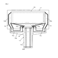
- Fig. 1 is a view showing the whole organic EL module and Figs. 2 to 4 are enlarged views of an important portion of the organic EL module.
- a part of respective wirings described later is omitted.
- a support substrate 11 is an electrically insulating substrate made of a rectangular transparent glass material.
- a light-emitting display 12 and a driver IC 13 are provided on the support substrate 11.
- An FPC 14 is installed on the support substrate 11 as a means for electrically connecting to the driver IC 13.
- anode wirings 15 connected to respective anode lines of the light-emitting display 12 described later, a first wiring 16a and a second wiring 16b that are some parts of cathode wirings 16 connected to respective cathode lines of the light-emitting display 12 described later, and an input wiring 17 for electrically connecting the driver IC 13 to an external circuit are formed on the support substrate 11.
- a sealing material for hermetically covering the light-emitting display 12 is provided on the support substrate 11, the sealing material is omitted in Figs. 1 , 3 , and 4 .
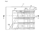
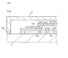
- the light-emitting display 12 mainly includes plural anode lines (first electrode lines) 12a, an insulating film 12b, a partition wall 12c, an organic layer 12d, and plural cathode lines (second electrode lines) 12e, as illustrated in Figs. 2 and 3 , and it is what is called a passive matrix light-emitting display including plural light-emitting pixels (organic EL element) which are formed by intersecting the respective anode lines 12a and the respective cathode lines 12e and interposing the organic layer 12d therebetween. Further, the light-emitting display 12 is hermetically covered by a sealing material 12f, as illustrated in Fig. 3 .
- the anode lines 12a are made of a transparent conductive material such as ITO. After the conductive material is formed into a layer shape on the support substrate 11 through vapor deposition, sputtering, and the like, the anode lines 12a are formed in almost parallel through a photolithography method and the like. One ends (the lower side in Fig. 1 ) of the respective anode lines 12a are connected to the respective anode wirings 15.
- the insulating film 12b is made of an electrically insulating polyimide material, for example, and positioned between the anode lines 12a and the cathode lines 12e, hence to prevent short of the both electrode lines 12a and 12e.
- the insulating film 12b is provided with openings 12b1 which define and clearly outline the respective light-emitting pixels. Further, the insulating film 12b is extended between the cathode wirings 16 and the cathode lines 12e and provided with contact holes 12b2 which connect the respective cathode wirings 16 to the respective cathode lines 12e.
- the partition wall 12c is made of an electrically insulating phenolic material, for example, and formed on the insulating film 12b.
- the partition wall 12c is formed so that its cross section has an inverted taper shape with respect to the insulating film 12b, according to the photolithography and the like.
- the plural partition walls 12c are formed in a direction orthogonal to the anode lines 12a at regular intervals.
- the partition wall 12c is designed to decouple the organic layer 12d and the cathode lines 12e when forming the organic layer 12d and the cathode lines 12e through the vapor deposition, sputtering and the like from above.
- the organic layer 12d is formed on the anode lines 12a and at least provided with an organic light-emitting layer.
- the organic layer 12d is formed by sequentially stacking a hole injection layer, a hole transport layer, the organic light-emitting layer, and an electron transport layer through the vapor deposition, sputtering, and the like.
- the plural cathode lines 12e are formed of a metal conductive material such as aluminum (Al), and magnesium silver (Mg : Ag) having a higher conductivity than that of the anode lines 12a, through the vapor deposition or the like, in a way of intersecting with the respective anode lines 12a.
- the respective cathode lines 12e are connected to the respective second wirings 16b through the contact holes 12b2 provided on the insulating film 12b.
- the sealing material 12f is formed of, for example, a glass material and provided on the support substrate 1 through a bonding agent 12g, in order to hermetically accommodate the light-emitting display 12.
- the driver IC 13 forms a driving circuit which makes the light-emitting display 12 emit a light and includes a signal line driving circuit, a scanning line driving circuit, and the like.
- the driver IC 13 is provided on the support substrate 11 in accordance with the light-emitting display 12 through a COG technique and electrically connected to the respective anode lines 12a and the respective cathode lines 12e through the respective anode wirings 15 and the respective cathode wirings 16, to apply a drive current between the respective anode lines 12a and the respective cathode lines 12e.
- the FPC 14 is a flexible circuit board, which is formed into a substantially T-letter shape, provided with a connecting wiring 18 to be connected to the input wiring 17 on a central portion 14a, and provided with third wirings 16c that are some parts of the cathode wirings 16 to be connected to the cathode lines 12e on the light-emitting display 12, in both lateral portions 14b.
- the connecting wirings 18 and the third wirings 16c formed on the back side of the FPC 14 are shown by a dotted line.
- the anode wiring 15 is a wiring for connecting the anode line 12a to the driver IC 13 and formed of a conductive material of, for example, ITO that is the same material as that of the anode line 12a, chrome (Cr), aluminum (Al), or the like, or a stack of these conductive materials.
- the anode wirings 15 are formed on the support substrate 11 integrally with the anode lines 12a, or formed separately so as to be connected to the anode lines 12a.
- the cathode wiring 16 is a wiring for connecting the cathode line 12e to the driver IC and formed by first and second wirings 16a and 16b that are metal wirings formed on the support substrate 11 and the third wiring 16c that is a copper foil wiring formed on the FPC 14.
- the first and second wirings 16a and 16b are decoupled on the support substrate 11 and connected to each other through the third wiring 16c on the FPC 14.
- the first and second wirings 16a and 16b are formed of a conductive material of, for example, ITO that is the same material as that of the anode line 12a, chrome (Cr), aluminum (Al), or the like, or a stack of these conductive materials.
- the first wirings 16a are wirings formed near the driver IC 13 on the support substrate 11, with their one ends connected to the driver IC 13 and the other ends connected to the third wirings 16c through an anisotropic conductive film (ACF).
- the second wirings 16b are wirings which are drawn alternately on both sides of the cathode lines 12e on the lateral sides of the support substrate 11, with their one ends connected to the cathode lines 12e and the other ends connected to the third wirings 16c through the ACF.
- Each of the second wirings 16b is formed in such a way that at least its end portion that is a connecting portion to the cathode line 12e is positioned below the cathode line 12e through the insulating film 12b so as to be connectable to the cathode line 12e through the contact hole 12b2, as illustrated in Fig. 2 .
- the third wirings 16c are wirings formed on the lateral portions 14b of the substantially T-letter shaped FPC 14, which are made of, for example, a copper foil with a layer thickness of several to dozens ⁇ m, in which electric resistance in the same length is smaller than that of the metal wiring of the first and second wirings 16a and 16b.
- One end of the third wiring 16c is connected to the first wiring 16a through the ACF and the other end is connected to the second wiring 16b through the ACF.
- both ends of the third wirings 16c are connected to plural connecting units 14c formed in rows on one side of the FPC 14 (the upper side in Fig. 4 ) and connected to the first and second wirings 16a and 16b through the connecting units 14c.
- Intervals (pitch) between the connecting units 14c are not even and the intervals between the connecting units 14c are set wider on the lateral sides than the intervals between the connecting units 14c in a middle portion.
- the connecting units 14 are formed so that the intervals between the connecting units 14c to be connected to the second wirings 16b become wider than the intervals between the connecting units 14c to be connected to the first wirings 16a.
- positional deviation caused by thermal deformation expansion or shrinkage
- the input wiring 17 is a wiring for electrically connecting the driver IC 13 to the external circuit and formed of a conductive material of, for example, ITO that is the same material as that of the anode line 12a, chrome (Cr), aluminum (Al), or the like, or a stack of these conductive materials.
- the input wiring 17 is drawn and formed near the driver IC 13 on the support substrate 11, with one end connected to the driver IC 13 and the other end connected to the connecting wiring 18 formed on the FPC 14 through the ACF.
- the connecting wiring 18 is a wiring formed on the central portion 14a of the FPC 14 and formed of a copper foil, for example, with a layer thickness of several to dozens ⁇ m.
- the connecting wiring 18 has a terminal 18a with one end connected to the input wiring 17 through the ACF and the other end connected to the external circuit.
- the organic EL module is formed by the above mentioned units.
- the cathode wirings 16 in which large currents flow are separated into the first wiring 16a and the second wiring 16b on the support substrate 11, which are connected to each other through the third wiring 16c formed on the FPC 14.
- the third wiring 16c formed on the FPC 14 is formed of a copper foil with a thickness of several to dozens ⁇ m, much thicker compared with the wiring having the layer thickness of several nm formed on the support substrate 11, and the electric resistance is lower. Therefore, compared with the conventional case of extending all the cathode wirings 6 on the support substrate 1, it is possible to reduce wiring resistance in the cathode wirings 16, restrain a voltage drop, and improve the brightness of the light-emitting pixels.
- the cathode wirings 16 are constituted in that the first and second wirings 16a and 16b decoupled on the support substrate 11 are connected to each other through the third wirings 16c formed on the FPC 14, the invention is not restricted to this application but it may be applied to the anode wirings 15 or the input wiring 17 depending on the design of drawing wirings.
- a first wiring with one end connected to the driver IC 13 and a second wiring with one end connected to the anode line 12a are decoupled on the support substrate 11 and connected to each other through a third wiring formed on the FPC 14.
- the invention is applied to the input wiring, a first wiring with one end connected to the driver IC and a second wiring with one end connected to the external circuit are decoupled on the support substrate 11 and connected to each other through a third wiring formed on the FPC 14.
- the intervals between the connecting units 14c to connect the third wiring 16c to the first and second wirings 16a and 16b, which are formed on the FPC 14, wider on the lateral sides than the intervals in the middle portion, it is possible to restrain a contact failure caused by the positional deviation in the connecting units 14c as mentioned above.
- the invention is suitable for a COG typed organic EL module.
Landscapes
- Electroluminescent Light Sources (AREA)
- Devices For Indicating Variable Information By Combining Individual Elements (AREA)
Abstract
Description
- The invention relates to an organic EL module which is provided with a light-emitting display having plural first electrode lines formed on a support substrate, an organic light-emitting layer formed on the first electrode lines, and plural second electrode lines formed so as to intersect with the first electrode lines.
- As the conventional organic EL panels, there has been known a type of having a light-emitting display which has organic EL elements formed on a transparent support substrate as light-emitting pixels, the organic EL elements being formed by interposing an organic layer at least having an organic light-emitting layer between anode lines (first electrode lines) formed of ITO (Indium Tin Oxide) and the like and cathode lines (second electrode lines) formed of aluminum (Al) and the like (for example, refer to Patent Document 1). The organic EL element injects a hole from the anode and injects an electron from the cathode; and the hole and the electron are re-coupled in the organic light-emitting layer, hence to emit a light. The organic EL element has a so-called diode characteristic that a current hardly flows from the cathode to the anode.
- As a method of installing a driver IC for driving the organic EL element, there has been known a COG (Chip on Glass) mode of directly mounting the driver IC on the support substrate (for example, refer to Patent Document 2). A COG typed organic EL module is superior in downsizing.
-
- Patent Document 1:
JP-A-8-315981 - Patent Document 2:
JP-A-2000-40585 -
Fig. 5 shows a COG typed organic EL module. A light-emittingdisplay 2 and adriver IC 3 are provided on asupport substrate 1. Further, an FPC (Flexible Printed Circuit) 4 is installed on thesupport substrate 1 as an electrically connecting means to thedriver IC 3. Although a sealing material for hermetically covering the light-emittingdisplay 2 is provided on thesupport substrate 1, the sealing material is omitted inFig. 5 . In the COG typed organic EL module, hitherto fore,plural anode wirings 5 for connecting respective anode lines of the light-emitting display 2 to thedriver IC 3,plural cathode wirings 6 for connecting respective cathode lines of the light-emitting display 2 to thedriver IC 3, and an input wiring 7 for connecting thedriver IC 3 to an external circuit are drawn and formed on thesupport substrate 1. The input wiring 7 is connected to a connectingwiring 8 formed on theFPC 4. InFig. 5 , a part of theanode wirings 5, thecathode wirings 6, and the input wiring 7 is omitted. - The
anode wirings 5 and thecathode wirings 6 formed on thesupport substrate 1, however, are some hundreds nm thin in conductor thickness and large in resistance. According as thinner the wiring width gets, the larger the resistance becomes, and as a result, a voltage drop becomes large. In this case, brightness of an organic EL element is reduced disadvantageously because of a restriction in a driving voltage of thedriver IC 3. The number of theanode wirings 5 and thecathode wirings 6 is increased according as the number of dots of light-emitting pixels on the light-emittingdisplay 2 gets larger and the width of the wiring per one wiring gets thinner. Particularly, when thecathode wirings 6 are drawn on the lateral sides of thesupport substrate 1, as illustrated inFig. 5 , the wiring length of thecathode wirings 6 gets longer than the length of theanode wirings 5, which causes a remarkable increase in wiring resistance. Depending on the design, there is a case in which theanode wirings 5 or the input wiring 7 may be drawn on the lateral sides of thesupport substrate 1. - Taking the above mentioned problem into consideration, the invention aims to provide an organic EL module capable of improving brightness of an organic EL element, by reducing wiring resistance and restraining a voltage drop in a COG typed organic EL module.
- In order to solve the problem, the invention is an organic EL module having a light-emitting display including plural first electrode lines formed on a support substrate, an organic light-emitting layer formed on the first electrode lines, and plural second electrode lines formed so as to intersect with the first electrode lines, a driver IC which is provided on the support substrate for applying a drive current between the first and second electrode lines, and a circuit board which is installed on the support substrate for connecting the driver IC to an external circuit, in which a first wiring with its one end connected to the driver IC and a second wiring decoupled from the first wiring are formed on the support substrate, and the first wiring is connected to the second wiring through a third wiring formed on the circuit board.
- The second wiring is formed with one end connected to the first electrode lines or the second electrode lines and the other end connected to the third wiring.
- The second wiring is formed with one end connected to the external circuit and the other end connected to the third wiring.
- On the circuit board, plural connecting units for connecting the third wiring to the first and second wirings are formed in rows on one side and intervals between the connecting units are wider on the lateral sides than intervals between the connecting units in a middle portion.
- The circuit board is a flexible substrate.
- As mentioned above, according to the invention, in a COG typed organic EL module, by reducing wiring resistance, it is possible to restrain a voltage drop and to improve brightness of an organic EL element.
-
- [
Fig. 1] Fig. 1 is a view showing an organic EL module of an embodiment of the invention. - [
Fig. 2] Fig. 2 is an enlarged view of an important portion of the organic EL module. - [
Fig. 3] Fig. 3 is a cross-sectional view showing an organic EL element indicating the organic EL module. - [
Fig. 4] Fig. 4 is an enlarged view of an important portion of the organic EL module. - [
Fig. 5] Fig. 5 is a view showing the conventional organic EL module. - Hereinafter, an organic EL module that is an embodiment of the invention will be described according to the attached drawings.
Fig. 1 is a view showing the whole organic EL module andFigs. 2 to 4 are enlarged views of an important portion of the organic EL module. In the drawings, a part of respective wirings described later is omitted. - A
support substrate 11 is an electrically insulating substrate made of a rectangular transparent glass material. A light-emitting display 12 and adriver IC 13 are provided on thesupport substrate 11. An FPC 14 is installed on thesupport substrate 11 as a means for electrically connecting to thedriver IC 13. Further,anode wirings 15 connected to respective anode lines of the light-emittingdisplay 12 described later, afirst wiring 16a and asecond wiring 16b that are some parts ofcathode wirings 16 connected to respective cathode lines of the light-emittingdisplay 12 described later, and aninput wiring 17 for electrically connecting thedriver IC 13 to an external circuit are formed on thesupport substrate 11. Although a sealing material for hermetically covering the light-emittingdisplay 12 is provided on thesupport substrate 11, the sealing material is omitted inFigs. 1 ,3 , and4 . - The light-emitting
display 12 mainly includes plural anode lines (first electrode lines) 12a, aninsulating film 12b, a partition wall 12c, anorganic layer 12d, and plural cathode lines (second electrode lines) 12e, as illustrated inFigs. 2 and3 , and it is what is called a passive matrix light-emitting display including plural light-emitting pixels (organic EL element) which are formed by intersecting therespective anode lines 12a and therespective cathode lines 12e and interposing theorganic layer 12d therebetween. Further, the light-emittingdisplay 12 is hermetically covered by a sealingmaterial 12f, as illustrated inFig. 3 . - The
anode lines 12a are made of a transparent conductive material such as ITO. After the conductive material is formed into a layer shape on thesupport substrate 11 through vapor deposition, sputtering, and the like, theanode lines 12a are formed in almost parallel through a photolithography method and the like. One ends (the lower side inFig. 1 ) of therespective anode lines 12a are connected to therespective anode wirings 15. - The
insulating film 12b is made of an electrically insulating polyimide material, for example, and positioned between theanode lines 12a and thecathode lines 12e, hence to prevent short of the bothelectrode lines insulating film 12b is provided with openings 12b1 which define and clearly outline the respective light-emitting pixels. Further, theinsulating film 12b is extended between thecathode wirings 16 and thecathode lines 12e and provided with contact holes 12b2 which connect therespective cathode wirings 16 to therespective cathode lines 12e. - The partition wall 12c is made of an electrically insulating phenolic material, for example, and formed on the
insulating film 12b. The partition wall 12c is formed so that its cross section has an inverted taper shape with respect to theinsulating film 12b, according to the photolithography and the like. The plural partition walls 12c are formed in a direction orthogonal to theanode lines 12a at regular intervals. The partition wall 12c is designed to decouple theorganic layer 12d and thecathode lines 12e when forming theorganic layer 12d and thecathode lines 12e through the vapor deposition, sputtering and the like from above. - The
organic layer 12d is formed on theanode lines 12a and at least provided with an organic light-emitting layer. In this embodiment, theorganic layer 12d is formed by sequentially stacking a hole injection layer, a hole transport layer, the organic light-emitting layer, and an electron transport layer through the vapor deposition, sputtering, and the like. - The
plural cathode lines 12e are formed of a metal conductive material such as aluminum (Al), and magnesium silver (Mg : Ag) having a higher conductivity than that of theanode lines 12a, through the vapor deposition or the like, in a way of intersecting with therespective anode lines 12a. Therespective cathode lines 12e are connected to the respectivesecond wirings 16b through the contact holes 12b2 provided on theinsulating film 12b. - The sealing
material 12f is formed of, for example, a glass material and provided on thesupport substrate 1 through abonding agent 12g, in order to hermetically accommodate the light-emittingdisplay 12. - The
driver IC 13 forms a driving circuit which makes the light-emittingdisplay 12 emit a light and includes a signal line driving circuit, a scanning line driving circuit, and the like. Thedriver IC 13 is provided on thesupport substrate 11 in accordance with the light-emittingdisplay 12 through a COG technique and electrically connected to therespective anode lines 12a and therespective cathode lines 12e through therespective anode wirings 15 and therespective cathode wirings 16, to apply a drive current between therespective anode lines 12a and therespective cathode lines 12e. - The
FPC 14 is a flexible circuit board, which is formed into a substantially T-letter shape, provided with a connectingwiring 18 to be connected to theinput wiring 17 on acentral portion 14a, and provided withthird wirings 16c that are some parts of the cathode wirings 16 to be connected to thecathode lines 12e on the light-emittingdisplay 12, in bothlateral portions 14b. InFig. 1 , the connectingwirings 18 and thethird wirings 16c formed on the back side of theFPC 14 are shown by a dotted line. - The
anode wiring 15 is a wiring for connecting theanode line 12a to thedriver IC 13 and formed of a conductive material of, for example, ITO that is the same material as that of theanode line 12a, chrome (Cr), aluminum (Al), or the like, or a stack of these conductive materials. The anode wirings 15 are formed on thesupport substrate 11 integrally with theanode lines 12a, or formed separately so as to be connected to theanode lines 12a. - The
cathode wiring 16 is a wiring for connecting thecathode line 12e to the driver IC and formed by first andsecond wirings support substrate 11 and thethird wiring 16c that is a copper foil wiring formed on theFPC 14. The first andsecond wirings support substrate 11 and connected to each other through thethird wiring 16c on theFPC 14. - The first and
second wirings anode line 12a, chrome (Cr), aluminum (Al), or the like, or a stack of these conductive materials. Thefirst wirings 16a are wirings formed near thedriver IC 13 on thesupport substrate 11, with their one ends connected to thedriver IC 13 and the other ends connected to thethird wirings 16c through an anisotropic conductive film (ACF). Thesecond wirings 16b are wirings which are drawn alternately on both sides of thecathode lines 12e on the lateral sides of thesupport substrate 11, with their one ends connected to thecathode lines 12e and the other ends connected to thethird wirings 16c through the ACF. Each of thesecond wirings 16b is formed in such a way that at least its end portion that is a connecting portion to thecathode line 12e is positioned below thecathode line 12e through the insulatingfilm 12b so as to be connectable to thecathode line 12e through the contact hole 12b2, as illustrated inFig. 2 . - The
third wirings 16c are wirings formed on thelateral portions 14b of the substantially T-letter shapedFPC 14, which are made of, for example, a copper foil with a layer thickness of several to dozens µm, in which electric resistance in the same length is smaller than that of the metal wiring of the first andsecond wirings third wiring 16c is connected to thefirst wiring 16a through the ACF and the other end is connected to thesecond wiring 16b through the ACF. As illustrated inFig. 4 , both ends of thethird wirings 16c are connected to plural connectingunits 14c formed in rows on one side of the FPC 14 (the upper side inFig. 4 ) and connected to the first andsecond wirings units 14c. Intervals (pitch) between the connectingunits 14c are not even and the intervals between the connectingunits 14c are set wider on the lateral sides than the intervals between the connectingunits 14c in a middle portion. Namely, in the embodiment, the connectingunits 14 are formed so that the intervals between the connectingunits 14c to be connected to thesecond wirings 16b become wider than the intervals between the connectingunits 14c to be connected to thefirst wirings 16a. In theFPC 14 formed wider, positional deviation caused by thermal deformation (expansion or shrinkage) is larger on the lateral sides than in the middle portion. Therefore, by widening the intervals between the connectingunits 14c on the lateral sides, it is possible to restrain a contact malfunction of the connectingunits 14c caused by the positional deviation. - The
input wiring 17 is a wiring for electrically connecting thedriver IC 13 to the external circuit and formed of a conductive material of, for example, ITO that is the same material as that of theanode line 12a, chrome (Cr), aluminum (Al), or the like, or a stack of these conductive materials. Theinput wiring 17 is drawn and formed near thedriver IC 13 on thesupport substrate 11, with one end connected to thedriver IC 13 and the other end connected to the connectingwiring 18 formed on theFPC 14 through the ACF. - The connecting
wiring 18 is a wiring formed on thecentral portion 14a of theFPC 14 and formed of a copper foil, for example, with a layer thickness of several to dozens µm. The connectingwiring 18 has a terminal 18a with one end connected to theinput wiring 17 through the ACF and the other end connected to the external circuit. - The organic EL module is formed by the above mentioned units.
- In the organic EL module, of the wirings extended from the
driver IC 13, thecathode wirings 16 in which large currents flow are separated into thefirst wiring 16a and thesecond wiring 16b on thesupport substrate 11, which are connected to each other through thethird wiring 16c formed on theFPC 14. Thethird wiring 16c formed on theFPC 14 is formed of a copper foil with a thickness of several to dozens µm, much thicker compared with the wiring having the layer thickness of several nm formed on thesupport substrate 11, and the electric resistance is lower. Therefore, compared with the conventional case of extending all thecathode wirings 6 on thesupport substrate 1, it is possible to reduce wiring resistance in thecathode wirings 16, restrain a voltage drop, and improve the brightness of the light-emitting pixels. In this embodiment, although thecathode wirings 16 are constituted in that the first andsecond wirings support substrate 11 are connected to each other through thethird wirings 16c formed on theFPC 14, the invention is not restricted to this application but it may be applied to theanode wirings 15 or theinput wiring 17 depending on the design of drawing wirings. When the invention is applied to theanode wirings 15, a first wiring with one end connected to thedriver IC 13 and a second wiring with one end connected to theanode line 12a are decoupled on thesupport substrate 11 and connected to each other through a third wiring formed on theFPC 14. When the invention is applied to the input wiring, a first wiring with one end connected to the driver IC and a second wiring with one end connected to the external circuit are decoupled on thesupport substrate 11 and connected to each other through a third wiring formed on theFPC 14. - Further, by making the intervals between the connecting
units 14c to connect thethird wiring 16c to the first andsecond wirings FPC 14, wider on the lateral sides than the intervals in the middle portion, it is possible to restrain a contact failure caused by the positional deviation in the connectingunits 14c as mentioned above. - The invention is suitable for a COG typed organic EL module.
-
- 11
- support substrate
- 12
- light-emitting display
- 12a
- anode line (first electrode line)
- 12b
- insulating film
- 12c
- partition wall
- 12d
- organic layer
- 12e
- cathode line (second electrode line)
- 12f
- sealing material
- 13
- driver IC
- 14
- FPC
- 15
- anode wiring
- 16
- cathode wiring
- 16a
- first wiring
- 16b
- second wiring
- 16c
- third wiring
- 17
- input wiring
- 18
- connecting wiring
Claims (5)
- An organic EL module comprising:a light-emitting display including a plurality of first electrode lines formed on a support substrate, an organic light-emitting layer formed on the first electrode lines, and a plurality of second electrode lines formed so as to intersect with the first electrode lines,a driver IC which is provided on the support substrate for applying a drive current between the first and the second electrode lines, anda circuit board which is installed on the support substrate for connecting the driver IC to an external circuit, whereina first wiring with one end connected to the driver IC and a second wiring decoupled from the first wiring are formed on the support substrate, andthe first wiring is connected to the second wiring through a third wiring formed on the circuit board.
- The organic EL module according to Claim 1, wherein the second wiring is formed with one end connected to the first electrode lines or the second electrode lines and with the other end connected to the third wiring.
- The organic EL module according to Claim 1, wherein the second wiring is formed with one end connected to the external circuit and the other end connected to the third wiring.
- The organic EL module according to Claim 1, wherein on the circuit board, a plurality of connecting units for connecting the third wiring to the first and the second wirings are formed in rows on one side, and intervals between the connecting units are wider on lateral sides than intervals between the connecting units in a middle portion.
- The organic EL module according to Claim 1, wherein the circuit board is a flexible substrate.
Applications Claiming Priority (2)
| Application Number | Priority Date | Filing Date | Title |
|---|---|---|---|
| JP2009249701A JP5477626B2 (en) | 2009-10-30 | 2009-10-30 | Organic EL module |
| PCT/JP2010/068107 WO2011052397A1 (en) | 2009-10-30 | 2010-10-15 | Organic el module |
Publications (3)
| Publication Number | Publication Date |
|---|---|
| EP2496053A1 true EP2496053A1 (en) | 2012-09-05 |
| EP2496053A4 EP2496053A4 (en) | 2013-11-06 |
| EP2496053B1 EP2496053B1 (en) | 2019-04-10 |
Family
ID=43921823
Family Applications (1)
| Application Number | Title | Priority Date | Filing Date |
|---|---|---|---|
| EP10826531.5A Not-in-force EP2496053B1 (en) | 2009-10-30 | 2010-10-15 | Organic el module |
Country Status (4)
| Country | Link |
|---|---|
| US (1) | US20120206067A1 (en) |
| EP (1) | EP2496053B1 (en) |
| JP (1) | JP5477626B2 (en) |
| WO (1) | WO2011052397A1 (en) |
Families Citing this family (2)
| Publication number | Priority date | Publication date | Assignee | Title |
|---|---|---|---|---|
| JP5471317B2 (en) * | 2009-11-05 | 2014-04-16 | 日本精機株式会社 | Organic EL panel |
| JP6612406B2 (en) * | 2018-09-05 | 2019-11-27 | パイオニア株式会社 | Light emitting device |
Family Cites Families (14)
| Publication number | Priority date | Publication date | Assignee | Title |
|---|---|---|---|---|
| JPH051265U (en) * | 1991-06-20 | 1993-01-08 | カシオ計算機株式会社 | Board wiring structure |
| JP3813217B2 (en) | 1995-03-13 | 2006-08-23 | パイオニア株式会社 | Method for manufacturing organic electroluminescence display panel |
| JP2000040585A (en) | 1998-07-21 | 2000-02-08 | Tdk Corp | Organic EL element module |
| JP4179313B2 (en) * | 2001-09-21 | 2008-11-12 | セイコーエプソン株式会社 | Electro-optical panel, electro-optical device and electronic apparatus |
| JP2003295785A (en) * | 2002-04-03 | 2003-10-15 | Optrex Corp | Organic EL display device and driving device thereof |
| JP3938367B2 (en) * | 2002-09-03 | 2007-06-27 | シャープ株式会社 | Electronic module and drive circuit board used therefor |
| JP4314084B2 (en) * | 2002-09-17 | 2009-08-12 | シャープ株式会社 | Display device |
| JP2004163827A (en) * | 2002-11-15 | 2004-06-10 | Denso Corp | Transparent display device |
| JP4144387B2 (en) * | 2003-03-13 | 2008-09-03 | セイコーエプソン株式会社 | Electro-optical device and electronic apparatus |
| US7411601B2 (en) * | 2004-08-03 | 2008-08-12 | Seiko Epson Corporation | Exposure head |
| JP4736614B2 (en) * | 2005-08-12 | 2011-07-27 | セイコーエプソン株式会社 | Signal transmission circuit, electro-optical device, and electronic apparatus |
| JP4926426B2 (en) * | 2005-08-12 | 2012-05-09 | 株式会社半導体エネルギー研究所 | Electronics |
| JP2008209792A (en) * | 2007-02-27 | 2008-09-11 | Optrex Corp | Liquid crystal display device |
| JP5157602B2 (en) * | 2008-04-03 | 2013-03-06 | セイコーエプソン株式会社 | Electro-optical device and electronic apparatus |
-
2009
- 2009-10-30 JP JP2009249701A patent/JP5477626B2/en not_active Expired - Fee Related
-
2010
- 2010-10-15 US US13/503,602 patent/US20120206067A1/en not_active Abandoned
- 2010-10-15 EP EP10826531.5A patent/EP2496053B1/en not_active Not-in-force
- 2010-10-15 WO PCT/JP2010/068107 patent/WO2011052397A1/en not_active Ceased
Also Published As
| Publication number | Publication date |
|---|---|
| JP5477626B2 (en) | 2014-04-23 |
| EP2496053A4 (en) | 2013-11-06 |
| US20120206067A1 (en) | 2012-08-16 |
| EP2496053B1 (en) | 2019-04-10 |
| JP2011096524A (en) | 2011-05-12 |
| WO2011052397A1 (en) | 2011-05-05 |
Similar Documents
| Publication | Publication Date | Title |
|---|---|---|
| EP3648189B1 (en) | Electroluminescent diode array substrate, preparation method thereof and display panel | |
| EP2764401B1 (en) | Interconnection schemes for displays with minimized border regions | |
| CN109411455B (en) | LED display unit group and display panel | |
| US11887947B2 (en) | Electronic device including conductive element on side surface of substrate | |
| US8143527B2 (en) | Golden finger for flexible printed circuitboard | |
| EP3633661A1 (en) | Electronic device | |
| US12057382B2 (en) | Chip on film assembly, display panel, and display module | |
| US7095476B2 (en) | Liquid crystal module | |
| CN110308815A (en) | Display panel and display device | |
| CN211654825U (en) | Array substrate, display panel and wiring structure thereof | |
| CN107678196A (en) | Connector and display screen | |
| KR102808240B1 (en) | Electronic device | |
| JP5982060B2 (en) | Passive matrix drive display and tiling display | |
| EP2496053B1 (en) | Organic el module | |
| US8067889B2 (en) | Stacked display medium | |
| KR20060130265A (en) | Display | |
| US8680791B2 (en) | Organic EL panel | |
| JP2003223988A (en) | Organic el panel | |
| JP5471691B2 (en) | Organic EL panel | |
| JP7638091B2 (en) | Display device and manufacturing method thereof | |
| JP2011187217A (en) | Organic el module | |
| JP2010170773A (en) | Organic el panel | |
| CN218039209U (en) | OLED display panel and display device | |
| JP2015225092A (en) | Display device | |
| JP2020025033A (en) | Flexible wiring board and display device |
Legal Events
| Date | Code | Title | Description |
|---|---|---|---|
| PUAI | Public reference made under article 153(3) epc to a published international application that has entered the european phase |
Free format text: ORIGINAL CODE: 0009012 |
|
| 17P | Request for examination filed |
Effective date: 20120504 |
|
| AK | Designated contracting states |
Kind code of ref document: A1 Designated state(s): AL AT BE BG CH CY CZ DE DK EE ES FI FR GB GR HR HU IE IS IT LI LT LU LV MC MK MT NL NO PL PT RO RS SE SI SK SM TR |
|
| DAX | Request for extension of the european patent (deleted) | ||
| A4 | Supplementary search report drawn up and despatched |
Effective date: 20131004 |
|
| RIC1 | Information provided on ipc code assigned before grant |
Ipc: G09F 9/30 20060101ALI20130927BHEP Ipc: G09F 9/00 20060101ALI20130927BHEP Ipc: H01L 51/50 20060101ALI20130927BHEP Ipc: H01L 27/32 20060101ALI20130927BHEP Ipc: H05B 33/06 20060101ALI20130927BHEP Ipc: H05B 33/02 20060101AFI20130927BHEP |
|
| REG | Reference to a national code |
Ref country code: DE Ref legal event code: R079 Ref document number: 602010058205 Country of ref document: DE Free format text: PREVIOUS MAIN CLASS: H05B0033020000 Ipc: H01L0027320000 |
|
| GRAP | Despatch of communication of intention to grant a patent |
Free format text: ORIGINAL CODE: EPIDOSNIGR1 |
|
| STAA | Information on the status of an ep patent application or granted ep patent |
Free format text: STATUS: GRANT OF PATENT IS INTENDED |
|
| RIC1 | Information provided on ipc code assigned before grant |
Ipc: H01L 27/32 20060101AFI20181022BHEP |
|
| INTG | Intention to grant announced |
Effective date: 20181114 |
|
| GRAS | Grant fee paid |
Free format text: ORIGINAL CODE: EPIDOSNIGR3 |
|
| GRAA | (expected) grant |
Free format text: ORIGINAL CODE: 0009210 |
|
| STAA | Information on the status of an ep patent application or granted ep patent |
Free format text: STATUS: THE PATENT HAS BEEN GRANTED |
|
| AK | Designated contracting states |
Kind code of ref document: B1 Designated state(s): AL AT BE BG CH CY CZ DE DK EE ES FI FR GB GR HR HU IE IS IT LI LT LU LV MC MK MT NL NO PL PT RO RS SE SI SK SM TR |
|
| REG | Reference to a national code |
Ref country code: GB Ref legal event code: FG4D |
|
| REG | Reference to a national code |
Ref country code: CH Ref legal event code: EP Ref country code: AT Ref legal event code: REF Ref document number: 1119846 Country of ref document: AT Kind code of ref document: T Effective date: 20190415 |
|
| REG | Reference to a national code |
Ref country code: DE Ref legal event code: R096 Ref document number: 602010058205 Country of ref document: DE |
|
| REG | Reference to a national code |
Ref country code: IE Ref legal event code: FG4D |
|
| REG | Reference to a national code |
Ref country code: NL Ref legal event code: MP Effective date: 20190410 |
|
| REG | Reference to a national code |
Ref country code: LT Ref legal event code: MG4D |
|
| REG | Reference to a national code |
Ref country code: AT Ref legal event code: MK05 Ref document number: 1119846 Country of ref document: AT Kind code of ref document: T Effective date: 20190410 |
|
| PG25 | Lapsed in a contracting state [announced via postgrant information from national office to epo] |
Ref country code: NL Free format text: LAPSE BECAUSE OF FAILURE TO SUBMIT A TRANSLATION OF THE DESCRIPTION OR TO PAY THE FEE WITHIN THE PRESCRIBED TIME-LIMIT Effective date: 20190410 |
|
| PG25 | Lapsed in a contracting state [announced via postgrant information from national office to epo] |
Ref country code: NO Free format text: LAPSE BECAUSE OF FAILURE TO SUBMIT A TRANSLATION OF THE DESCRIPTION OR TO PAY THE FEE WITHIN THE PRESCRIBED TIME-LIMIT Effective date: 20190710 Ref country code: FI Free format text: LAPSE BECAUSE OF FAILURE TO SUBMIT A TRANSLATION OF THE DESCRIPTION OR TO PAY THE FEE WITHIN THE PRESCRIBED TIME-LIMIT Effective date: 20190410 Ref country code: PT Free format text: LAPSE BECAUSE OF FAILURE TO SUBMIT A TRANSLATION OF THE DESCRIPTION OR TO PAY THE FEE WITHIN THE PRESCRIBED TIME-LIMIT Effective date: 20190910 Ref country code: ES Free format text: LAPSE BECAUSE OF FAILURE TO SUBMIT A TRANSLATION OF THE DESCRIPTION OR TO PAY THE FEE WITHIN THE PRESCRIBED TIME-LIMIT Effective date: 20190410 Ref country code: SE Free format text: LAPSE BECAUSE OF FAILURE TO SUBMIT A TRANSLATION OF THE DESCRIPTION OR TO PAY THE FEE WITHIN THE PRESCRIBED TIME-LIMIT Effective date: 20190410 Ref country code: AL Free format text: LAPSE BECAUSE OF FAILURE TO SUBMIT A TRANSLATION OF THE DESCRIPTION OR TO PAY THE FEE WITHIN THE PRESCRIBED TIME-LIMIT Effective date: 20190410 Ref country code: HR Free format text: LAPSE BECAUSE OF FAILURE TO SUBMIT A TRANSLATION OF THE DESCRIPTION OR TO PAY THE FEE WITHIN THE PRESCRIBED TIME-LIMIT Effective date: 20190410 Ref country code: LT Free format text: LAPSE BECAUSE OF FAILURE TO SUBMIT A TRANSLATION OF THE DESCRIPTION OR TO PAY THE FEE WITHIN THE PRESCRIBED TIME-LIMIT Effective date: 20190410 |
|
| PG25 | Lapsed in a contracting state [announced via postgrant information from national office to epo] |
Ref country code: RS Free format text: LAPSE BECAUSE OF FAILURE TO SUBMIT A TRANSLATION OF THE DESCRIPTION OR TO PAY THE FEE WITHIN THE PRESCRIBED TIME-LIMIT Effective date: 20190410 Ref country code: PL Free format text: LAPSE BECAUSE OF FAILURE TO SUBMIT A TRANSLATION OF THE DESCRIPTION OR TO PAY THE FEE WITHIN THE PRESCRIBED TIME-LIMIT Effective date: 20190410 Ref country code: GR Free format text: LAPSE BECAUSE OF FAILURE TO SUBMIT A TRANSLATION OF THE DESCRIPTION OR TO PAY THE FEE WITHIN THE PRESCRIBED TIME-LIMIT Effective date: 20190711 Ref country code: BG Free format text: LAPSE BECAUSE OF FAILURE TO SUBMIT A TRANSLATION OF THE DESCRIPTION OR TO PAY THE FEE WITHIN THE PRESCRIBED TIME-LIMIT Effective date: 20190710 Ref country code: LV Free format text: LAPSE BECAUSE OF FAILURE TO SUBMIT A TRANSLATION OF THE DESCRIPTION OR TO PAY THE FEE WITHIN THE PRESCRIBED TIME-LIMIT Effective date: 20190410 |
|
| PG25 | Lapsed in a contracting state [announced via postgrant information from national office to epo] |
Ref country code: AT Free format text: LAPSE BECAUSE OF FAILURE TO SUBMIT A TRANSLATION OF THE DESCRIPTION OR TO PAY THE FEE WITHIN THE PRESCRIBED TIME-LIMIT Effective date: 20190410 Ref country code: IS Free format text: LAPSE BECAUSE OF FAILURE TO SUBMIT A TRANSLATION OF THE DESCRIPTION OR TO PAY THE FEE WITHIN THE PRESCRIBED TIME-LIMIT Effective date: 20190810 |
|
| REG | Reference to a national code |
Ref country code: DE Ref legal event code: R097 Ref document number: 602010058205 Country of ref document: DE |
|
| PG25 | Lapsed in a contracting state [announced via postgrant information from national office to epo] |
Ref country code: CZ Free format text: LAPSE BECAUSE OF FAILURE TO SUBMIT A TRANSLATION OF THE DESCRIPTION OR TO PAY THE FEE WITHIN THE PRESCRIBED TIME-LIMIT Effective date: 20190410 Ref country code: EE Free format text: LAPSE BECAUSE OF FAILURE TO SUBMIT A TRANSLATION OF THE DESCRIPTION OR TO PAY THE FEE WITHIN THE PRESCRIBED TIME-LIMIT Effective date: 20190410 Ref country code: RO Free format text: LAPSE BECAUSE OF FAILURE TO SUBMIT A TRANSLATION OF THE DESCRIPTION OR TO PAY THE FEE WITHIN THE PRESCRIBED TIME-LIMIT Effective date: 20190410 Ref country code: DK Free format text: LAPSE BECAUSE OF FAILURE TO SUBMIT A TRANSLATION OF THE DESCRIPTION OR TO PAY THE FEE WITHIN THE PRESCRIBED TIME-LIMIT Effective date: 20190410 Ref country code: SK Free format text: LAPSE BECAUSE OF FAILURE TO SUBMIT A TRANSLATION OF THE DESCRIPTION OR TO PAY THE FEE WITHIN THE PRESCRIBED TIME-LIMIT Effective date: 20190410 |
|
| PLBE | No opposition filed within time limit |
Free format text: ORIGINAL CODE: 0009261 |
|
| STAA | Information on the status of an ep patent application or granted ep patent |
Free format text: STATUS: NO OPPOSITION FILED WITHIN TIME LIMIT |
|
| PG25 | Lapsed in a contracting state [announced via postgrant information from national office to epo] |
Ref country code: IT Free format text: LAPSE BECAUSE OF FAILURE TO SUBMIT A TRANSLATION OF THE DESCRIPTION OR TO PAY THE FEE WITHIN THE PRESCRIBED TIME-LIMIT Effective date: 20190410 Ref country code: SM Free format text: LAPSE BECAUSE OF FAILURE TO SUBMIT A TRANSLATION OF THE DESCRIPTION OR TO PAY THE FEE WITHIN THE PRESCRIBED TIME-LIMIT Effective date: 20190410 |
|
| 26N | No opposition filed |
Effective date: 20200113 |
|
| PG25 | Lapsed in a contracting state [announced via postgrant information from national office to epo] |
Ref country code: TR Free format text: LAPSE BECAUSE OF FAILURE TO SUBMIT A TRANSLATION OF THE DESCRIPTION OR TO PAY THE FEE WITHIN THE PRESCRIBED TIME-LIMIT Effective date: 20190410 |
|
| REG | Reference to a national code |
Ref country code: DE Ref legal event code: R119 Ref document number: 602010058205 Country of ref document: DE |
|
| PG25 | Lapsed in a contracting state [announced via postgrant information from national office to epo] |
Ref country code: SI Free format text: LAPSE BECAUSE OF FAILURE TO SUBMIT A TRANSLATION OF THE DESCRIPTION OR TO PAY THE FEE WITHIN THE PRESCRIBED TIME-LIMIT Effective date: 20190410 Ref country code: MC Free format text: LAPSE BECAUSE OF FAILURE TO SUBMIT A TRANSLATION OF THE DESCRIPTION OR TO PAY THE FEE WITHIN THE PRESCRIBED TIME-LIMIT Effective date: 20190410 |
|
| REG | Reference to a national code |
Ref country code: CH Ref legal event code: PL |
|
| PG25 | Lapsed in a contracting state [announced via postgrant information from national office to epo] |
Ref country code: CH Free format text: LAPSE BECAUSE OF NON-PAYMENT OF DUE FEES Effective date: 20191031 Ref country code: LU Free format text: LAPSE BECAUSE OF NON-PAYMENT OF DUE FEES Effective date: 20191015 Ref country code: LI Free format text: LAPSE BECAUSE OF NON-PAYMENT OF DUE FEES Effective date: 20191031 Ref country code: DE Free format text: LAPSE BECAUSE OF NON-PAYMENT OF DUE FEES Effective date: 20200501 |
|
| REG | Reference to a national code |
Ref country code: BE Ref legal event code: MM Effective date: 20191031 |
|
| PG25 | Lapsed in a contracting state [announced via postgrant information from national office to epo] |
Ref country code: BE Free format text: LAPSE BECAUSE OF NON-PAYMENT OF DUE FEES Effective date: 20191031 |
|
| GBPC | Gb: european patent ceased through non-payment of renewal fee |
Effective date: 20191015 |
|
| PG25 | Lapsed in a contracting state [announced via postgrant information from national office to epo] |
Ref country code: IE Free format text: LAPSE BECAUSE OF NON-PAYMENT OF DUE FEES Effective date: 20191015 Ref country code: GB Free format text: LAPSE BECAUSE OF NON-PAYMENT OF DUE FEES Effective date: 20191015 Ref country code: FR Free format text: LAPSE BECAUSE OF NON-PAYMENT OF DUE FEES Effective date: 20191031 |
|
| PG25 | Lapsed in a contracting state [announced via postgrant information from national office to epo] |
Ref country code: CY Free format text: LAPSE BECAUSE OF FAILURE TO SUBMIT A TRANSLATION OF THE DESCRIPTION OR TO PAY THE FEE WITHIN THE PRESCRIBED TIME-LIMIT Effective date: 20190410 |
|
| PG25 | Lapsed in a contracting state [announced via postgrant information from national office to epo] |
Ref country code: HU Free format text: LAPSE BECAUSE OF FAILURE TO SUBMIT A TRANSLATION OF THE DESCRIPTION OR TO PAY THE FEE WITHIN THE PRESCRIBED TIME-LIMIT; INVALID AB INITIO Effective date: 20101015 Ref country code: MT Free format text: LAPSE BECAUSE OF FAILURE TO SUBMIT A TRANSLATION OF THE DESCRIPTION OR TO PAY THE FEE WITHIN THE PRESCRIBED TIME-LIMIT Effective date: 20190410 |
|
| PG25 | Lapsed in a contracting state [announced via postgrant information from national office to epo] |
Ref country code: MK Free format text: LAPSE BECAUSE OF FAILURE TO SUBMIT A TRANSLATION OF THE DESCRIPTION OR TO PAY THE FEE WITHIN THE PRESCRIBED TIME-LIMIT Effective date: 20190410 |