EP2493008A1 - Transmission line, impedance transformer, integrated circuit mounted device, and communication device module - Google Patents
Transmission line, impedance transformer, integrated circuit mounted device, and communication device module Download PDFInfo
- Publication number
- EP2493008A1 EP2493008A1 EP11190255A EP11190255A EP2493008A1 EP 2493008 A1 EP2493008 A1 EP 2493008A1 EP 11190255 A EP11190255 A EP 11190255A EP 11190255 A EP11190255 A EP 11190255A EP 2493008 A1 EP2493008 A1 EP 2493008A1
- Authority
- EP
- European Patent Office
- Prior art keywords
- line
- lines
- tapered
- integrated circuit
- opposite
- Prior art date
- Legal status (The legal status is an assumption and is not a legal conclusion. Google has not performed a legal analysis and makes no representation as to the accuracy of the status listed.)
- Granted
Links
Images




Classifications
-
- H—ELECTRICITY
- H01—ELECTRIC ELEMENTS
- H01P—WAVEGUIDES; RESONATORS, LINES, OR OTHER DEVICES OF THE WAVEGUIDE TYPE
- H01P5/00—Coupling devices of the waveguide type
- H01P5/12—Coupling devices having more than two ports
-
- H—ELECTRICITY
- H01—ELECTRIC ELEMENTS
- H01P—WAVEGUIDES; RESONATORS, LINES, OR OTHER DEVICES OF THE WAVEGUIDE TYPE
- H01P5/00—Coupling devices of the waveguide type
- H01P5/02—Coupling devices of the waveguide type with invariable factor of coupling
-
- H—ELECTRICITY
- H01—ELECTRIC ELEMENTS
- H01P—WAVEGUIDES; RESONATORS, LINES, OR OTHER DEVICES OF THE WAVEGUIDE TYPE
- H01P3/00—Waveguides; Transmission lines of the waveguide type
- H01P3/02—Waveguides; Transmission lines of the waveguide type with two longitudinal conductors
- H01P3/08—Microstrips; Strip lines
-
- H—ELECTRICITY
- H03—ELECTRONIC CIRCUITRY
- H03F—AMPLIFIERS
- H03F3/00—Amplifiers with only discharge tubes or only semiconductor devices as amplifying elements
- H03F3/60—Amplifiers in which coupling networks have distributed constants, e.g. with waveguide resonators
- H03F3/602—Combinations of several amplifiers
-
- H—ELECTRICITY
- H03—ELECTRONIC CIRCUITRY
- H03H—IMPEDANCE NETWORKS, e.g. RESONANT CIRCUITS; RESONATORS
- H03H7/00—Multiple-port networks comprising only passive electrical elements as network components
- H03H7/38—Impedance-matching networks
-
- H—ELECTRICITY
- H04—ELECTRIC COMMUNICATION TECHNIQUE
- H04B—TRANSMISSION
- H04B1/00—Details of transmission systems, not covered by a single one of groups H04B3/00 - H04B13/00; Details of transmission systems not characterised by the medium used for transmission
-
- H—ELECTRICITY
- H10—SEMICONDUCTOR DEVICES; ELECTRIC SOLID-STATE DEVICES NOT OTHERWISE PROVIDED FOR
- H10W—GENERIC PACKAGES, INTERCONNECTIONS, CONNECTORS OR OTHER CONSTRUCTIONAL DETAILS OF DEVICES COVERED BY CLASS H10
- H10W44/00—Electrical arrangements for controlling or matching impedance
- H10W44/20—Electrical arrangements for controlling or matching impedance at high-frequency [HF] or radio frequency [RF]
-
- H—ELECTRICITY
- H10—SEMICONDUCTOR DEVICES; ELECTRIC SOLID-STATE DEVICES NOT OTHERWISE PROVIDED FOR
- H10W—GENERIC PACKAGES, INTERCONNECTIONS, CONNECTORS OR OTHER CONSTRUCTIONAL DETAILS OF DEVICES COVERED BY CLASS H10
- H10W44/00—Electrical arrangements for controlling or matching impedance
- H10W44/20—Electrical arrangements for controlling or matching impedance at high-frequency [HF] or radio frequency [RF]
- H10W44/203—Electrical connections
- H10W44/216—Waveguides, e.g. strip lines
-
- H—ELECTRICITY
- H10—SEMICONDUCTOR DEVICES; ELECTRIC SOLID-STATE DEVICES NOT OTHERWISE PROVIDED FOR
- H10W—GENERIC PACKAGES, INTERCONNECTIONS, CONNECTORS OR OTHER CONSTRUCTIONAL DETAILS OF DEVICES COVERED BY CLASS H10
- H10W44/00—Electrical arrangements for controlling or matching impedance
- H10W44/20—Electrical arrangements for controlling or matching impedance at high-frequency [HF] or radio frequency [RF]
- H10W44/226—Electrical arrangements for controlling or matching impedance at high-frequency [HF] or radio frequency [RF] for HF amplifiers
- H10W44/234—Arrangements for impedance matching
-
- H—ELECTRICITY
- H10—SEMICONDUCTOR DEVICES; ELECTRIC SOLID-STATE DEVICES NOT OTHERWISE PROVIDED FOR
- H10W—GENERIC PACKAGES, INTERCONNECTIONS, CONNECTORS OR OTHER CONSTRUCTIONAL DETAILS OF DEVICES COVERED BY CLASS H10
- H10W72/00—Interconnections or connectors in packages
- H10W72/50—Bond wires
- H10W72/541—Dispositions of bond wires
- H10W72/5445—Dispositions of bond wires being orthogonal to a side surface of the chip, e.g. parallel arrangements
Definitions
- the embodiments discussed herein are related to a transmission line, an impedance transformer including a transmission line, an integrated circuit mounted device including an impedance transformer, and a communication device module including an integrated circuit mounted device.
- a high-output integrated circuit device that mounts an integrated circuit chip including a high-output transistor is demanded for a mobile telephone base station or radar.
- high-output characteristics are realized by arranging in parallel a plurality of power transistors formed on an integrated circuit chip on a metal package and forming an impedance transformer by a line on a dielectric substrate for impedance matching.
- an impedance transformer In order to form a wideband matching circuit, an impedance transformer is utilized, in which a plurality of 1/4 wavelength lines is connected in series so as to keep a Q value small. Such an impedance transformer is used widely in an integrated circuit mounted device that requires wideband characteristics because the wideband characteristics may be obtained by increasing the number of stages of the 1/4 wavelength line.
- a transmission line having a desired characteristic impedance is formed with the substrate thickness of the wire, the dielectric constant of the substrate, and the wire width being taken into consideration.
- Figs. 1A and 1B are diagrams explaining impedance conversion, wherein Fig. 1A illustrates a case of matching with one stage and Fig. 1B illustrates a case of matching with two stages. It is assumed that the output impedance of a transistor is R1, the input impedance in the subsequent stage is R0, and R0>R1 holds.
- R1 the output impedance of a transistor
- R0 the input impedance in the subsequent stage
- R0>R1 holds.
- Z1 (R1 3 xR0) 1 ⁇ 4
- the gate width of a transistor is increased in order to increase the output.
- the increase in the gate width of a transistor may be realized by using a plurality of transistors having the same characteristics in parallel and connecting the outputs of the plurality of transistors commonly. If the gate width of the transistor is increased in this manner, the output impedance of the transistor is reduced to 1 ⁇ or less.
- the output impedance of several ohms is converted into 50 ⁇ used normally and to perform impedance matching. In this case, in order to secure the frequency band, as illustrated in Fig.
- a plurality of impedance transformers are connected in series and the impedance is converted into 50 ⁇ stepwise for matching.
- the shape of the 1/4 wavelength line is determined based on the dielectric constant, the impedance, etc., of the substrate. Because of this, a high-impedance line that uses a substrate with a low dielectric constant has a longer length and a wider width compared to a low-impedance line that uses a substrate with a high dielectric constant. As a result, there is such a problem that the size of the matching circuit is increased. Because of this, a pattern layout in which a long line is bent in wiring is used to downsize the matching circuit.
- a compact transmission line a compact impedance transformer, an integrated circuit mounted device and a communication device module are realized.
- a transmission line includes two tapered lines having a tapered planar shape and arranged in parallel, an opposite line provided in opposition to the narrower width sides of the two tapered lines, and bonding wires for connecting the narrower width sides of the two tapered lines and the opposite line, wherein the distance between two outer edges on the narrower width sides of the two tapered lines arranged in parallel is greater than the distance between outer edges on the opposite side of the opposite line in opposition to the narrower width sides of the two tapered lines.
- Fig. 2 is a diagram illustrating a conventional example of a matching circuit of a high-output integrated circuit mounted device including a line in a bent shape.
- an integrated circuit chip 11 includes a plurality of transistors.
- the left side of the integrated circuit chip 11 is an input matching circuit 20 and the right side is an output matching circuit 30.
- the input matching circuit 20 includes a 1/4 wavelength line 22 in a bent shape formed on a substrate 21, a 1/4 wavelength line in a linear shape formed on a substrate 23, bonding wires 25 for connecting the 1/4 wavelength line 22 and the 1/4 wavelength line 24, and bonding wires 26 for connecting the 1/4 wavelength line 24 and the input terminal of the integrated circuit chip 11.
- the output matching circuit 30 includes an electrode 32 in a tapered shape formed on a substrate 31, a 1/4 wavelength line 34 in a linear shape formed on a substrate 33, a 1/4 wavelength line 36 in a bent shape formed on a substrate 35, bonding wires 37 for connecting the output terminal of the integrated circuit chip 11 and the electrode 32, bonding wires 38 for connecting the electrode 32 and the 1/4 wavelength line 34, and bonding wires 39 for connecting the 1/4 wavelength line 34 and the 1/4 wavelength line 36.
- An end part OUT on the right side of the 1/4 wavelength line 36 is an output part and which is connected to the terminal of the package of the integrated circuit mounted device with bonding wires etc.
- connection is usually realized by bonding wires.
- the integrated circuit chip 11 and the 1/4 wavelength line 24, and the integrated circuit chip 11 and the 1/4 wavelength line 32 are connected by eight bonding wires 26 and 37, respectively.
- four bonding wires 25 are used and for the connection of the electrode 32 and the 1/4 wavelength line 34 and the connection of the 1/4 wavelength line 34 and the 1/4 wavelength line 36, four bonding wires 38 and 39 are respectively used.
- the plurality of wires is bonded using the same bonding device with the bonding positions shifted in parallel. Consequently, the trace of the boded wire projected on the bonding plane (line) extends in parallel.
- the wire is parallel.
- a transistor chip in which power transistors formed on a semiconductor chip are arranged in parallel in a plurality of rows on a metal package is used.
- a matching circuit is arranged at the input/output of the transistor chip.
- the matching circuit is a line on a dielectric substrate and configured by an impedance converter and realizes high-output characteristics by impedance-matching the transistor.
- the gate width of the transistor is made wider. By inputting the same signal into a plurality of transistors and commonly connecting the outputs of the plurality of transistors, the gate width of the transistor is substantially made wider and the increase in output is realized.
- the number of parallel connections of transistors within the chip is increased and a plurality of chips is arranged in an alignment manner to compose power. If the number of parallel connections of transistors within the chip is increased, the transverse width size of the chip is increased accordingly and the length between the output parts (pads) at both ends of the transistor chip is increased. Further, also when a plurality of chips is arranged in an alignment manner, the length between the output parts located at both ends is increased. It is desirable to form a matching circuit to extract an output from such a transistor chip or a plurality of chips without deteriorating the output performance of the transistor.
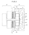
- Fig. 3 is a diagram illustrating an example of a circuit arrangement supposed when an output matching circuit using two chips and having a line in a bent shape illustrated in Fig. 2 is applied. It is desirable to consider an input matching circuit into consideration, however, the input matching circuit may be realized by, for example, arranging the output matching circuit in a symmetric manner, and therefore, in order to make explanation simple, only the output matching circuit is explained.
- reference numeral 20 represents an input matching circuit and 30 an output matching circuit. As described above, explanation of the input matching circuit 20 is omitted.
- two chips 11A and 11B are arranged so that the output terminal of each transistor is arranged in a line, in other words, the chips 11A and 11B are arranged side by side.
- the output matching circuit 30 has low dielectric constant substrates 31A and 31B, high dielectric constant substrates 33A and 33B, and the low dielectric constant substrate 35.
- a tapered line 32 having a tapered (trapezoidal) planar shape is formed.
- a tapered line 32B having a tapered (trapezoidal) planar shape is formed.
- a low impedance line 34A having a linear (rectangular) planar shape is formed.
- a low impedance line 34B having a linear (rectangular) planar shape is formed.
- high impedance lines 36A and 36B for impedance-matching the outputs of the low impedance lines 34A and 34B and composing them at the out OUT are formed. It is desirable to insert a resistor between the inputs of the high impedance lines 36A and 36B to suppress trouble, such as circuit oscillation due to the variation in packaging.
- the positions of the input terminals of the high impedance lines 36A and 36B are apart, and therefore, connection lines 40A and 40B are extended from the input terminals of the high impedance lines 36A and 36B and connected with a resistor 41.
- the wider width side (the longer base of the trapezoid) of the tapered line 32A is in opposition to the chip 11A and connected by the bonding wires.
- the wider width side (the longer base of the trapezoid)of the tapered line 32B is in opposition to the chip 11B and connected by the bonding wires.
- the length of the chip 11A and the width of the longer base of the tapered line 32A, and the length of the chip 11B and the width of the longer base of the tapered line 32B are substantially the same, and therefore, the bonding wires are parallel.
- the narrower width side (the shorter base of the trapezoid) of the tapered line 32A is in opposition to the low impedance line 34A and connected by the bonding wire wires.
- the narrower width side (the shorter base of the trapezoid) of the tapered line 32B is in opposition to the low impedance line 34B and connected by the bonding wires.
- the width of the shorter base of the tapered line 32A and the width of the low impedance line 34A, and the width of the shorter base of the tapered line 32B and the width of the low impedance line 34B are substantially the same, and therefore, the bonding wires are parallel.
- the low impedance line 34A is in opposition to the high impedance line 36A and connected by the bonding wires.
- the low impedance line 34B is in opposition to the high impedance line 36B and connected by the bonding wires.
- the bonding wires for connecting the lines are substantially parallel.
- the widths and lengths of the tapered lines 32A and 32B, the low impedance lines 34A and 34B, and the high impedance lines 36A and 36B are determined to realize impedance matching according to the dielectric constant of the substrate.
- the tapered line formed on the low dielectric constant substrate has a tapered (trapezoidal) planar shape and at the end on the opposite side of the chip, the width of the wire is made narrower than the width size of the chip.
- the signal path length of the signal output from both end parts of the chip differs from that of the signal output from the chip center part. Therefore, at high frequencies in particular, the signals cancel each other out and it becomes difficult to extract a signal efficiently. As a result, the output, efficiency, and the frequency band are reduced. Further, it is difficult to fine-adjust the conventional circuit characteristic which impedes improvement of yields.
- a high-performance integrated circuit mounted device in which the difference in the signal path length between the signal output from both end parts of the chip and the signal output from the center part is reduced.
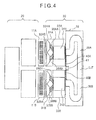
- Fig. 4 is a diagram illustrating a circuit arrangement of an integrated circuit mounted device in a first embodiment.
- the circuit arrangement of the integrated circuit mounted device in the first embodiment has the two chips 11A and 11B in which a plurality of transistors is arrayed in the form of a row, the input matching circuit 20, and the output matching circuit 30.
- the signal input from the input terminal of the input matching circuit 20 is input to the inputs of the transistors of the two chips in parallel while the input matching circuit 20 is maintaining impedance matching. Consequently, the same signal is input to the plurality of transistors and the plurality of transistors outputs the same output in parallel and at the same time to the output matching circuit 30.
- the output matching circuit 30 composes the signals input in parallel from the two chips 11A and 11B while maintaining impedance matching and outputs it from the output terminal OUT. Due to this, the gate width of the transistor is increased substantially and high output is realized.
- any type of the input matching circuit 20 may be used and its explanation is omitted.
- the output matching circuit 30 has the low dielectric constant substrates 31A and 31B, the high dielectric constant substrates 33A and 33B, and the low dielectric constant substrate 35.
- the low dielectric constant substrate 31A two tapered lines 32AA and 32AB having a tapered (trapezoidal) planar shape are formed.
- two tapered lines 32BA and 32BB having a tapered (trapezoidal) planar shape are formed.
- the high dielectric constant 33A the low impedance line 34A having a linear (rectangular) planar shape is formed.
- the low impedance line 34B having a linear (rectangular) planar shape is formed.
- the high impedance lines 36A and 36B are formed, which composes the outputs of the low impedance lines 34A and 34B after impedance-matching them at the output OUT. Further, on the low dielectric constant substrate 35, the connection lines 40A and 40B extending from the input terminals of the high impedance lines 36A and 36B and the resistor 41 connected between the connection lines 40A and 40B are arranged.
- the wider width sides (the longer base of the trapezoid) of the two tapered lines 32AA and 32AB are arranged side by side in the direction perpendicular to the direction in which the signal travels and in opposition to the chip 11A and connected by bonding wires.
- the wider width sides (the longer base of the trapezoid) of the two tapered lines 32BA and 32BB are arranged side by side in the direction perpendicular to the direction in which the signal travels and in opposition to the chip 11B and connected by bonding wires.
- the length of the chip 11A is substantially the same as the sum of the widths of the longer bases of the two tapered lines 32AA and 32AB and the bonding wires are parallel.
- the length of the chip 11B is substantially the same as the sum of the widths of the longer bases of the two tapered lines 32BA and 32BB and the bonding wires are parallel.
- the narrower width sides (the shorter base of the trapezoid) of the two tapered lines 32AA and 32AB are in opposition to the low impedance line 34A and connected by bonding wires.
- the narrower width sides (the shorter base of the trapezoid) of the two tapered lines 32BA and 32BB are in opposition to the low impedance line 34B and connected by bonding wires.
- the shorter bases of the two tapered lines 32AA and 32AB are arranged with a space and the distance between the upper end of the shorter base of the tapered line 32AA and the lower end of the shorter base of the tapered line 32AB is greater than the width of the low impedance line 34A. Because of this, bonding wires 38AA for connecting the tapered line 32AA and the low impedance line 34A and bonding wires 38AB for connecting the tapered line 32AB and the low impedance line 34A are not parallel. Specifically, the tapered line 32AA and the low impedance line 34A are connected by the five parallel wires 38AA and the tapered line 32AB and the low impedance line 34A are connected by the five parallel wires 38AB. However, the trace of the wire 38AA projected on the line plane extends in a direction different from a direction in which the trace of the wire 38AB projected on the line plane extends.
- the tapered line 32BA and the low impedance line 34B are connected by five parallel wires 38BA and the tapered line 32BB and the low impedance line 34B are connected by five parallel wires 38BB.
- the trace of the wire 38BA projected on the line plane extends in a direction different from a direction in which the trace of the wire 38BB projected on the line plane extends.
- the low impedance line 34A is in opposition to the high impedance line 36A and connected by bonding wires.
- the low impedance line 34B is in opposition to the high impedance line 36B and connected by bonding wires.
- the high impedance line 36A and the high impedance line 36B are connected at the output terminal OUT and an output may be obtained therefrom.
- the widths and lengths of the tapered lines 32AA, 32AB, 32BA, and 32BB, the low impedance lines 34A and 34B, and the high impedance lines 36A and 36B are determined to realize impedance matching according to the dielectric constant of the substrate.
- the circuit arrangement in the first embodiment differs from the circuit arrangement in Fig. 3 in that the tapered line is divided into two tapered lines and the shorter bases of the two tapered lines and the low impedance line are connected by the bonding wires extending in different directions and other parts are the same.
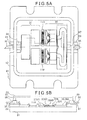
- Fig. 5A is a top view of the integrated circuit mounted device in the first embodiment and Fig. 5B is a sectional view at the part of the broken line in the top view.
- Figs. 5A and 5B illustrate a high-output amplifier circuit device mounting the circuit device in Fig. 4 in a hermetically sealed metal package having a metal wall.
- connection electrodes 84 and 87 are provided for electrical connection with the outside.
- the connection electrodes 84 and 87 are electrically insulated from the metal wall 82 and the lid 83 by field-throughs 86 and 89.
- an input lead 85 is provided and on the part outside the package of the connection electrode 87, an output lead 88 is provided.
- the part within the package of the connection electrode 84 and an input part IN of the input matching circuit 20 are connected by a boding wire etc.
- the part within the package of the connection electrode 88 and the output part OUT of the output matching circuit 30 are connected by bonding wires etc.
- two GaN (gallium nitride) power transistor (HEMT) chips and a matching circuit substrate (high dielectric substrate, low dielectric substrate) configuring an impedance converter are packaged in a nitrogen atmosphere at 300°C using, for example, AuSn. It is possible to use a metal having a relative dielectric constant of 9.8 as the low dielectric constant substrates 31A, 31B and a metal having a relative dielectric constant of 140 as the high dielectric constant substrates 33A, 33B. Due to this, for example, in the output matching circuit 30, it is possible to form an impedance converter for converting the output impedance of the transistor into 50 ohm by a transmission line having a desired characteristic impedance.
- the low impedance lines 34A, 34B formed on the high dielectric constant substrates 34A, 34B are formed to have a wire width of 2.4 mm.
- the wires are arranged at regular intervals along the length of the shorter base of the tapered line and the wires are connected so as to be symmetric vertically (symmetric with respect to the line in the direction in which the signal travels) as to the low impedance lines 34A, 34B on the high dielectric constant substrates 33A, 33B with the wire intervals being maintained.
- the wire length may be changed in minute units, and therefore, it is possible to fine-adjust the circuit characteristics by fine-adjusting the wire inductance, also contributing to improvement of performance and yields.
- the low impedance lines 34A, 34B are connected to the high impedance lines 36A, 36B of the low dielectric constant substrate 35.
- the low dielectric constant substrate 35 is a parallel line having a substrate thickness of 0.38 mm, a substrate dielectric constant of 9.8, and a wire width of 0.65 mm. It is possible to easily realize a transmission line of microwaves and millimeter waves by the micro strip line by making the back surface of the dielectric substrate a ground and the surface a signal wire, and therefore, design properties may be obtained.
- each line is connected by bonding wires, however, it is also possible to connect by a bonding ribbon.
- the bonding ribbons for connecting the shorter bases of the tapered lines 32AA and 32AB and the low impedance line 34A extend in different directions.
- the bonding ribbons for connecting the shorter bases of the tapered lines 32BA and 32BB and the low impedance line 34B extend in different directions.
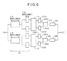
- Fig. 6 is a diagram schematically illustrating the impedance conversion circuit of the integrated circuit mounted device in the first embodiment.
- the input matching circuit 20 is arranged and to the other, the output matching circuit 30 is arranged.
- the input matching circuit 20 performs impedance conversion through the 1/4 wavelength circuit in two stages.
- the output matching circuit 30 also performs impedance conversion through the 1/4 wavelength circuit in two stages.
- the first stage of the output matching circuit 30 is formed by the tapered lines 32AA, 32AB, 32BA, and 32BB and the low impedance line 34 and the second stage by the high impedance lines 36A and 36B.
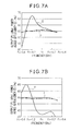
- Fig. 7A is a diagram illustrating measured characteristics of a test-manufacturing amplifier having the circuit arrangement in the first embodiment
- Fig. 7B is a diagram illustrating measured characteristics of a test-manufacturing amplifier having the circuit arrangement in Fig. 3 in order to confirm the effect of the circuit arrangement in the first embodiment.
- Fig. 8 is a diagram illustrating a circuit arrangement of an integrated circuit mounted device in a second embodiment.
- the circuit arrangement in the second embodiment differs in that the low impedance line 34A is divided into two low impedance lines 34AA and 34AB and the low impedance line 34B is divided into two low impedance lines 34BA and 34BB in the first embodiment and others are the same. Between the two low impedance lines 34AA and 34AB, a resistor 42A is provided and between the two low impedance lines 34BA and 34BB, a resistor 42B is provided.
- the lines are formed into parallel lines. Further, by inserting the resistors 42A and 42B between the parallel lines, a problem, such as circuit oscillation due to the variation in packaging, is suppressed.
- Fig. 9 is a diagram illustrating a circuit arrangement of an integrated circuit mounted device in a third embodiment.
- the circuit arrangement in the third embodiment differs in that a composing line 43A for composing the low impedance lines 34AA and 34AB and a composing line 43B for composing the low impedance lines 34BA and 34BB are provided in the second embodiment and others are the same.
- the resistor 42A is provided between the two low impedance lines 34AA and 34AB, the resistor 42A is provided and between the two low impedance lines 34BA and 34BB, the resistor 42B is provided, the effect as that in the first embodiment may be obtained.
- Fig. 10 is a diagram illustrating a circuit arrangement of an integrated circuit mounted device in a fourth embodiment.
- the circuit arrangement in the fourth embodiment differs in that the tapered lines 32AA, 32AB, 32BA, and 32BB are formed on the high dielectric constant substrates 33A and 33B on which the low impedance lines 34A and 34B are formed in the first embodiment and others are the same. Consequently, in the fourth embodiment, the low dielectric constant substrates 31A and 31 are not provided.
- Fig. 11 is a diagram illustrating a circuit arrangement of an integrated circuit mounted device in a fifth embodiment.
- the circuit arrangement in the fifth embodiment differs in that the shapes of the tapered lines 32AA, 32AB, 32BA, and 32BB are formed into shapes of the tapered lines 32A and 32B illustrated in Fig. 3 divided into symmetric shapes about the centers, respectively, in the first embodiment and others are the same. It may also be possible to connect resistors 49A and 49B between the tapered lines 32AA and 32AB and between the tapered lines 32BA and 32BB. Due to this, it is possible to suppress trouble, such as circuit oscillation due to the variation in packaging.
- Fig. 12 is a diagram illustrating a circuit arrangement of an integrated circuit mounted device in a sixth embodiment.
- the circuit arrangement in the sixth embodiment differs from that in the first embodiment in that the same arrangement as that of the output matching circuit 30 in the first embodiment is applied also to the input matching circuit 20.
- the configuration and operation in the input matching circuit 20 are symmetric with those of the output matching circuit 30 with respect to the chips 11A and 11B, and therefore, its explanation is omitted.
- circuit arrangements of the integrated circuit mounted devices in the embodiments are explained as above, however, there may also be various modified examples.
- the example of the low impedance line having a linear (rectangular) planar shape is explained, however, it is also possible to form it into a tapered shape.
- Fig. 13 illustrates a modified example, in which the low impedance line 34A is formed into a tapered shape in the circuit arrangement in the fourth embodiment.
- the configuration of the output matching circuit 30 explained in the second to fifth embodiments may also be applied to the input matching circuit 20. Further, it is also possible to apply the configuration in the embodiment explained above only to the input matching circuit or to apply different configurations to the output matching circuit 30 and the input matching circuit 20, or to apply a combination thereof.
- the GaN transistor is used, however, it is also possible to use transistors using Si, GaAs, InP, etc.
- the chip and the matching circuit substrate are packaged using AuSn, however, it may also be possible to package them using a conductive adhesive. In this case, it is possible to package at 200°C or less, and therefore, it is possible to suppress cracks resulting from a difference in thermal expansion coefficient between the package and the chip, matching circuit substrate, and capacitor and yields may be improved. Further, it is possible to package a device, such as InP, the heat resistance of which is comparatively poor, without deteriorating the characteristics. Furthermore, it is possible to apply a material, such as copper, having a large thermal expansion coefficient difference of the package material, excellent in heat dissipation properties, and therefore, it is possible to realize a circuit with a higher output.
- the embodiments it is made possible to reduce loss in the impedance conversion circuit and further to fine-adjust the characteristics of the impedance conversion circuit, and therefore, it is possible to realize an integrated circuit device at low cost by improving yields, which has higher performance, such as higher output, higher efficiency, and wider band.
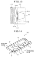
- Fig. 14 is a diagram illustrating a configuration of a communication device module 100 using the high-output amplifier circuit device in the embodiment.
- the communication device module 100 includes an input/output terminal 90 connected to an antenna, a transmission/reception switching device 91 connected with the input/output terminal 90, a lownoise amplifier 92, a control circuit 93, a previous stage amplifier 94, a high-output amplifier 95, and a filter 96.
- the row on the front-right side in Fig. 14 configures a transmission system and the rear-left side configures a reception system.
- An input signal from the input/output terminal 90 is selectively sent to the lownoise amplifier 92 by the transmission/reception switching device 91 and reception processing is performed.
- a transmission signal amplified in the previous-stage amplifier 94 is further amplified by the high-output amplifier 95 and selectively sent to the input/output terminal 90 by the transmission/reception switching device 91 through the filter 96 and transmitted from the antenna.
- the high-output amplifier 95 the high-output amplifier circuit device in the embodiment is used. It is needless to say that the high-output amplifier circuit device in the embodiment may be used not only in the transmission/reception communication module device but also in the transmission communication device module.
- the communication device module 100 in Fig. 14 is used as part of a system device, such as a communication system, radar, sensor, and radio interference unit.
- a system device such as a communication system, radar, sensor, and radio interference unit.
- the high-performance, compact high-output amplifier circuit device in the embodiment may contribute to the improvement of performance and downsizing of a device.
Landscapes
- Engineering & Computer Science (AREA)
- Power Engineering (AREA)
- Computer Networks & Wireless Communication (AREA)
- Signal Processing (AREA)
- Microwave Amplifiers (AREA)
- Amplifiers (AREA)
Abstract
Description
- The embodiments discussed herein are related to a transmission line, an impedance transformer including a transmission line, an integrated circuit mounted device including an impedance transformer, and a communication device module including an integrated circuit mounted device.
- Recently, a high-output integrated circuit device that mounts an integrated circuit chip including a high-output transistor is demanded for a mobile telephone base station or radar. In such an integrated circuit mounted device, high-output characteristics are realized by arranging in parallel a plurality of power transistors formed on an integrated circuit chip on a metal package and forming an impedance transformer by a line on a dielectric substrate for impedance matching.
- In order to form a wideband matching circuit, an impedance transformer is utilized, in which a plurality of 1/4 wavelength lines is connected in series so as to keep a Q value small. Such an impedance transformer is used widely in an integrated circuit mounted device that requires wideband characteristics because the wideband characteristics may be obtained by increasing the number of stages of the 1/4 wavelength line. When configuring a 1/4 wavelength impedance transformer, a transmission line having a desired characteristic impedance is formed with the substrate thickness of the wire, the dielectric constant of the substrate, and the wire width being taken into consideration.
-
Figs. 1A and 1B are diagrams explaining impedance conversion, whereinFig. 1A illustrates a case of matching with one stage andFig. 1B illustrates a case of matching with two stages. It is assumed that the output impedance of a transistor is R1, the input impedance in the subsequent stage is R0, and R0>R1 holds. When performing matching with one stage as illustrated inFig. 1A , one 1/4 wavelength line having a characteristic impedance Z is used and it is set as Z=(R0xR1)½ . In contrast to this, when performing matching with two stages as illustrated inFig. 1B , a 1/4 wavelength line having a characteristic impedance Z1 and a 1/4 wavelength line having a characteristic impedance Z2 are connected in series and they are set as Z1= (R13xR0)¼ and Z2=(R1xR03)¼. There is a case where 1/4 wavelength lines in three or more stages are connected in series. - In a high-output integrated circuit mounted device, the gate width of a transistor is increased in order to increase the output. The increase in the gate width of a transistor may be realized by using a plurality of transistors having the same characteristics in parallel and connecting the outputs of the plurality of transistors commonly. If the gate width of the transistor is increased in this manner, the output impedance of the transistor is reduced to 1 Ω or less. In order to increase the output of the transistor to the maximum, the output impedance of several ohms is converted into 50 Ω used normally and to perform impedance matching. In this case, in order to secure the frequency band, as illustrated in
Fig. 1B , a plurality of impedance transformers are connected in series and the impedance is converted into 50 Ω stepwise for matching. The shape of the 1/4 wavelength line, such as its length and width, is determined based on the dielectric constant, the impedance, etc., of the substrate. Because of this, a high-impedance line that uses a substrate with a low dielectric constant has a longer length and a wider width compared to a low-impedance line that uses a substrate with a high dielectric constant. As a result, there is such a problem that the size of the matching circuit is increased. Because of this, a pattern layout in which a long line is bent in wiring is used to downsize the matching circuit. - On the other hand, due to the recent development of broadband, the demand for large-capacity high-speed radio communication is increasing. It is expected that the third generation of the base station amplifier of a mobile telephone will become widely used in order to deal with a larger capacity and further the fourth generation will develop in the future. The new communication scheme (WiMAX) has been put into practical use and it is expected that an increase in capacity will develop. In such circumstances, a higher output, higher efficiency, wider band, and reduction in cost are demanded. On the other hand, for a radar amplifier, a higher output and wider band to improve performance, such as the extension of detection range and resolution, and further high efficiency to realize reduction in operation cost and downsizing of a cooler is demanded. Furthermore, in a phased array radar, it is necessary to arrange radar elements including an amplifier in the form of an array in a narrow space, and therefore, further downsizing of an amplifier is demanded.
-
- [Patent Document 1] Japanese Laid-open Patent Publication No.
H11-122009 - [Patent Document 2] Japanese Laid-open Patent Publication No.
H10-284920 - [Patent Document 3]
Japanese Laid-open Patent Publication No. S57-037903 - [Non-Patent Document 1] S. B. Cohn, "Optimum Design of Stepped Transmission-Line Transformers", IRE trans. MTT-3, pp.16-21, 1955.
- According to the embodiments, a compact transmission line, a compact impedance transformer, an integrated circuit mounted device and a communication device module are realized.
- According to an aspect of the embodiments, a transmission line includes two tapered lines having a tapered planar shape and arranged in parallel, an opposite line provided in opposition to the narrower width sides of the two tapered lines, and bonding wires for connecting the narrower width sides of the two tapered lines and the opposite line, wherein the distance between two outer edges on the narrower width sides of the two tapered lines arranged in parallel is greater than the distance between outer edges on the opposite side of the opposite line in opposition to the narrower width sides of the two tapered lines.
-
-
Figs. 1A and 1B are diagrams explaining impedance conversion; -
Fig. 2 is a diagram illustrating a conventional example of a matching circuit of a high-output integrated circuit mounted device including a line in a bent shape; -
Fig. 3 is a diagram illustrating an example of a circuit arrangement supposed when an output matching circuit using two chips and having a line in a bent shape illustrated inFig. 2 is applied; -
Fig. 4 is a diagram illustrating a circuit arrangement of an integrated circuit mounted device in a first embodiment; -
Fig. 5A is a top view of the integrated circuit mounted device in the first embodiment andFig. 5B is a sectional view of a part along a broken line in the top view; -
Fig. 6 is a diagram schematically illustrating an impedance conversion circuit of the integrated circuit mounted device in the first embodiment; -
Fig. 7A is a diagram illustrating a measured characteristic of an amplifier having the circuit arrangement in the first embodiment andFig. 7B is a diagram illustrating a measured characteristic of an amplifier having the circuit arrangement inFig. 3 , both the amplifiers being produced as prototypes; -
Fig. 8 is a diagram illustrating a circuit arrangement of an integrated circuit mounted device in a second embodiment; -
Fig. 9 is a diagram illustrating a circuit arrangement of the integrated circuit mounted device in the second embodiment; -
Fig. 10 is a diagram illustrating a circuit arrangement of an integrated circuit mounted device in a third embodiment; -
Fig. 11 is a diagram illustrating a circuit arrangement of an integrated circuit mounted device in a fourth embodiment; -
Fig. 12 is a diagram illustrating a circuit arrangement of an integrated circuit mounted device in a fifth embodiment; -
Fig. 13 illustrates a modified example when a low impedance line is formed into a tapered shape in the circuit arrangement in the fourth embodiment; and -
Fig. 14 is a diagram illustrating a configuration of a communication device module using a high-output amplifier circuit device. - Before explaining embodiments, the technology of increasing the output of and downsize of an integrated circuit mounted device will be explained.
-
Fig. 2 is a diagram illustrating a conventional example of a matching circuit of a high-output integrated circuit mounted device including a line in a bent shape. InFig. 2 , anintegrated circuit chip 11 includes a plurality of transistors. The left side of theintegrated circuit chip 11 is aninput matching circuit 20 and the right side is anoutput matching circuit 30. Theinput matching circuit 20 includes a 1/4wavelength line 22 in a bent shape formed on asubstrate 21, a 1/4 wavelength line in a linear shape formed on asubstrate 23,bonding wires 25 for connecting the 1/4wavelength line 22 and the 1/4wavelength line 24, andbonding wires 26 for connecting the 1/4wavelength line 24 and the input terminal of theintegrated circuit chip 11. An end part IN on the left side of the 1/4wavelength line 22 is an input part and which is connected to the terminal of the package of the integrated circuit mounted device with bonding wires, etc. Theoutput matching circuit 30 includes anelectrode 32 in a tapered shape formed on asubstrate 31, a 1/4wavelength line 34 in a linear shape formed on asubstrate 33, a 1/4wavelength line 36 in a bent shape formed on asubstrate 35,bonding wires 37 for connecting the output terminal of theintegrated circuit chip 11 and theelectrode 32,bonding wires 38 for connecting theelectrode 32 and the 1/4wavelength line 34, andbonding wires 39 for connecting the 1/4wavelength line 34 and the 1/4wavelength line 36. An end part OUT on the right side of the 1/4wavelength line 36 is an output part and which is connected to the terminal of the package of the integrated circuit mounted device with bonding wires etc. By using a line in a bent shape, it is possible to reduce the width of an integrated circuit mounted device in the direction in which a signal travels. - The connection is usually realized by bonding wires. For example, in the conventional example in
Fig. 2 , theintegrated circuit chip 11 and the 1/4wavelength line 24, and theintegrated circuit chip 11 and the 1/4wavelength line 32 are connected by eightbonding wires wavelength line 22 and the 1/4wavelength line 24, fourbonding wires 25 are used and for the connection of theelectrode 32 and the 1/4wavelength line 34 and the connection of the 1/4wavelength line 34 and the 1/4wavelength line 36, fourbonding wires - In a high-output semiconductor circuit, a transistor chip in which power transistors formed on a semiconductor chip are arranged in parallel in a plurality of rows on a metal package is used. In order to extract the performance of the transistor, a matching circuit is arranged at the input/output of the transistor chip. The matching circuit is a line on a dielectric substrate and configured by an impedance converter and realizes high-output characteristics by impedance-matching the transistor.
- In order to increase the output, the gate width of the transistor is made wider. By inputting the same signal into a plurality of transistors and commonly connecting the outputs of the plurality of transistors, the gate width of the transistor is substantially made wider and the increase in output is realized. At this time, the number of parallel connections of transistors within the chip is increased and a plurality of chips is arranged in an alignment manner to compose power. If the number of parallel connections of transistors within the chip is increased, the transverse width size of the chip is increased accordingly and the length between the output parts (pads) at both ends of the transistor chip is increased. Further, also when a plurality of chips is arranged in an alignment manner, the length between the output parts located at both ends is increased. It is desirable to form a matching circuit to extract an output from such a transistor chip or a plurality of chips without deteriorating the output performance of the transistor.
-
Fig. 3 is a diagram illustrating an example of a circuit arrangement supposed when an output matching circuit using two chips and having a line in a bent shape illustrated inFig. 2 is applied. It is desirable to consider an input matching circuit into consideration, however, the input matching circuit may be realized by, for example, arranging the output matching circuit in a symmetric manner, and therefore, in order to make explanation simple, only the output matching circuit is explained. - In
Fig. 3 ,reference numeral 20 represents an input matching circuit and 30 an output matching circuit. As described above, explanation of theinput matching circuit 20 is omitted. - As illustrated in
Fig. 3 , twochips chips - The
output matching circuit 30 has low dielectricconstant substrates constant substrates constant substrate 35. On the low dielectricconstant substrate 31A, a taperedline 32 having a tapered (trapezoidal) planar shape is formed. On the low dielectricconstant substrate 31B, atapered line 32B having a tapered (trapezoidal) planar shape is formed. On the high dielectricconstant substrate 33A, alow impedance line 34A having a linear (rectangular) planar shape is formed. On the high dielectricconstant substrate 33B, alow impedance line 34B having a linear (rectangular) planar shape is formed. On the low dielectricconstant substrate 35,high impedance lines low impedance lines high impedance lines high impedance lines connection lines high impedance lines resistor 41. - The wider width side (the longer base of the trapezoid) of the tapered
line 32A is in opposition to thechip 11A and connected by the bonding wires. The wider width side (the longer base of the trapezoid)of the taperedline 32B is in opposition to thechip 11B and connected by the bonding wires. The length of thechip 11A and the width of the longer base of the taperedline 32A, and the length of thechip 11B and the width of the longer base of the taperedline 32B are substantially the same, and therefore, the bonding wires are parallel. - The narrower width side (the shorter base of the trapezoid) of the tapered
line 32A is in opposition to thelow impedance line 34A and connected by the bonding wire wires. The narrower width side (the shorter base of the trapezoid) of the taperedline 32B is in opposition to thelow impedance line 34B and connected by the bonding wires. The width of the shorter base of the taperedline 32A and the width of thelow impedance line 34A, and the width of the shorter base of the taperedline 32B and the width of thelow impedance line 34B are substantially the same, and therefore, the bonding wires are parallel. - The
low impedance line 34A is in opposition to thehigh impedance line 36A and connected by the bonding wires. Thelow impedance line 34B is in opposition to thehigh impedance line 36B and connected by the bonding wires. - Therefore, in the output matching circuit in
Fig. 3 , the bonding wires for connecting the lines are substantially parallel. - The widths and lengths of the tapered
lines low impedance lines high impedance lines - As illustrated in
Fig. 2 andFig. 3 , the tapered line formed on the low dielectric constant substrate has a tapered (trapezoidal) planar shape and at the end on the opposite side of the chip, the width of the wire is made narrower than the width size of the chip. - However, when the tapered line is used, the signal path length of the signal output from both end parts of the chip differs from that of the signal output from the chip center part. Therefore, at high frequencies in particular, the signals cancel each other out and it becomes difficult to extract a signal efficiently. As a result, the output, efficiency, and the frequency band are reduced. Further, it is difficult to fine-adjust the conventional circuit characteristic which impedes improvement of yields.
- In the embodiment described below, a high-performance integrated circuit mounted device is provided, in which the difference in the signal path length between the signal output from both end parts of the chip and the signal output from the center part is reduced.
-
Fig. 4 is a diagram illustrating a circuit arrangement of an integrated circuit mounted device in a first embodiment. - The circuit arrangement of the integrated circuit mounted device in the first embodiment has the two
chips input matching circuit 20, and theoutput matching circuit 30. The signal input from the input terminal of theinput matching circuit 20 is input to the inputs of the transistors of the two chips in parallel while theinput matching circuit 20 is maintaining impedance matching. Consequently, the same signal is input to the plurality of transistors and the plurality of transistors outputs the same output in parallel and at the same time to theoutput matching circuit 30. Theoutput matching circuit 30 composes the signals input in parallel from the twochips input matching circuit 20 may be used and its explanation is omitted. - As illustrated in
Fig. 4 , theoutput matching circuit 30 has the low dielectricconstant substrates constant substrates constant substrate 35. On the low dielectricconstant substrate 31A, two tapered lines 32AA and 32AB having a tapered (trapezoidal) planar shape are formed. On the low dielectricconstant substrate 31B, two tapered lines 32BA and 32BB having a tapered (trapezoidal) planar shape are formed. On the high dielectric constant 33A, thelow impedance line 34A having a linear (rectangular) planar shape is formed. On the high dielectricconstant substrate 33B, thelow impedance line 34B having a linear (rectangular) planar shape is formed. On the low dielectricconstant substrate 35, thehigh impedance lines low impedance lines constant substrate 35, theconnection lines high impedance lines resistor 41 connected between theconnection lines - The wider width sides (the longer base of the trapezoid) of the two tapered lines 32AA and 32AB are arranged side by side in the direction perpendicular to the direction in which the signal travels and in opposition to the
chip 11A and connected by bonding wires. The wider width sides (the longer base of the trapezoid) of the two tapered lines 32BA and 32BB are arranged side by side in the direction perpendicular to the direction in which the signal travels and in opposition to thechip 11B and connected by bonding wires. The length of thechip 11A is substantially the same as the sum of the widths of the longer bases of the two tapered lines 32AA and 32AB and the bonding wires are parallel. Similarly, the length of thechip 11B is substantially the same as the sum of the widths of the longer bases of the two tapered lines 32BA and 32BB and the bonding wires are parallel. - The narrower width sides (the shorter base of the trapezoid) of the two tapered lines 32AA and 32AB are in opposition to the
low impedance line 34A and connected by bonding wires. The narrower width sides (the shorter base of the trapezoid) of the two tapered lines 32BA and 32BB are in opposition to thelow impedance line 34B and connected by bonding wires. - The shorter bases of the two tapered lines 32AA and 32AB are arranged with a space and the distance between the upper end of the shorter base of the tapered line 32AA and the lower end of the shorter base of the tapered line 32AB is greater than the width of the
low impedance line 34A. Because of this, bonding wires 38AA for connecting the tapered line 32AA and thelow impedance line 34A and bonding wires 38AB for connecting the tapered line 32AB and thelow impedance line 34A are not parallel. Specifically, the tapered line 32AA and thelow impedance line 34A are connected by the five parallel wires 38AA and the tapered line 32AB and thelow impedance line 34A are connected by the five parallel wires 38AB. However, the trace of the wire 38AA projected on the line plane extends in a direction different from a direction in which the trace of the wire 38AB projected on the line plane extends. - Similarly, the tapered line 32BA and the
low impedance line 34B are connected by five parallel wires 38BA and the tapered line 32BB and thelow impedance line 34B are connected by five parallel wires 38BB. However, the trace of the wire 38BA projected on the line plane extends in a direction different from a direction in which the trace of the wire 38BB projected on the line plane extends. - The
low impedance line 34A is in opposition to thehigh impedance line 36A and connected by bonding wires. Thelow impedance line 34B is in opposition to thehigh impedance line 36B and connected by bonding wires. Thehigh impedance line 36A and thehigh impedance line 36B are connected at the output terminal OUT and an output may be obtained therefrom. - The widths and lengths of the tapered lines 32AA, 32AB, 32BA, and 32BB, the
low impedance lines high impedance lines - As above, the circuit arrangement in the first embodiment differs from the circuit arrangement in
Fig. 3 in that the tapered line is divided into two tapered lines and the shorter bases of the two tapered lines and the low impedance line are connected by the bonding wires extending in different directions and other parts are the same. -
Fig. 5A is a top view of the integrated circuit mounted device in the first embodiment andFig. 5B is a sectional view at the part of the broken line in the top view.Figs. 5A and 5B illustrate a high-output amplifier circuit device mounting the circuit device inFig. 4 in a hermetically sealed metal package having a metal wall. - The package is hermetically sealed by a
metal wall 82 and alid 83 on ametal base 81. For electrical connection with the outside,connection electrodes connection electrodes metal wall 82 and thelid 83 by field-throughs connection electrode 84, aninput lead 85 is provided and on the part outside the package of theconnection electrode 87, anoutput lead 88 is provided. The part within the package of theconnection electrode 84 and an input part IN of theinput matching circuit 20 are connected by a boding wire etc. The part within the package of theconnection electrode 88 and the output part OUT of theoutput matching circuit 30 are connected by bonding wires etc. - On the
metal base 81, two GaN (gallium nitride) power transistor (HEMT) chips and a matching circuit substrate (high dielectric substrate, low dielectric substrate) configuring an impedance converter are packaged in a nitrogen atmosphere at 300°C using, for example, AuSn. It is possible to use a metal having a relative dielectric constant of 9.8 as the low dielectricconstant substrates constant substrates output matching circuit 30, it is possible to form an impedance converter for converting the output impedance of the transistor into 50 ohm by a transmission line having a desired characteristic impedance. Thelow impedance lines constant substrates low impedance lines constant substrates substrates substrates chips - The
low impedance lines high impedance lines constant substrate 35. The low dielectricconstant substrate 35 is a parallel line having a substrate thickness of 0.38 mm, a substrate dielectric constant of 9.8, and a wire width of 0.65 mm. It is possible to easily realize a transmission line of microwaves and millimeter waves by the micro strip line by making the back surface of the dielectric substrate a ground and the surface a signal wire, and therefore, design properties may be obtained. - In the above explanation, each line is connected by bonding wires, however, it is also possible to connect by a bonding ribbon. In this case also, the bonding ribbons for connecting the shorter bases of the tapered lines 32AA and 32AB and the
low impedance line 34A extend in different directions. Further, the bonding ribbons for connecting the shorter bases of the tapered lines 32BA and 32BB and thelow impedance line 34B extend in different directions. -
Fig. 6 is a diagram schematically illustrating the impedance conversion circuit of the integrated circuit mounted device in the first embodiment. To one of theintegrated circuit chips input matching circuit 20 is arranged and to the other, theoutput matching circuit 30 is arranged. Theinput matching circuit 20 performs impedance conversion through the 1/4 wavelength circuit in two stages. Similarly, theoutput matching circuit 30 also performs impedance conversion through the 1/4 wavelength circuit in two stages. The first stage of theoutput matching circuit 30 is formed by the tapered lines 32AA, 32AB, 32BA, and 32BB and thelow impedance line 34 and the second stage by thehigh impedance lines -
Fig. 7A is a diagram illustrating measured characteristics of a test-manufacturing amplifier having the circuit arrangement in the first embodiment andFig. 7B is a diagram illustrating measured characteristics of a test-manufacturing amplifier having the circuit arrangement inFig. 3 in order to confirm the effect of the circuit arrangement in the first embodiment. - As illustrated in
Fig. 7B , in the circuit arrangement inFig. 3 , the performance (output (P), power added efficiency (E)) in high frequencies is reduced. This is because the cancel-out of the signals immediately after output from the chips becomes remarkable in high frequencies in theoutput matching circuit 30. On the other hand, as illustrated inFig. 7A , in the circuit arrangement in the first embodiment, the cancel-out of signals immediately output from the chips is reduced and further, it is made possible to fine-adjust the characteristics, and therefore, it is known that the output and power added efficiency increase and the band is widened due to the improvement of the characteristics in high frequencies. Due to this, the effect in the first embodiment has been confirmed. -
Fig. 8 is a diagram illustrating a circuit arrangement of an integrated circuit mounted device in a second embodiment. - The circuit arrangement in the second embodiment differs in that the
low impedance line 34A is divided into two low impedance lines 34AA and 34AB and thelow impedance line 34B is divided into two low impedance lines 34BA and 34BB in the first embodiment and others are the same. Between the two low impedance lines 34AA and 34AB, aresistor 42A is provided and between the two low impedance lines 34BA and 34BB, aresistor 42B is provided. - As the frequency increases and it becomes no longer possible to ignore the line width for the signal wavelength, a mode other than a desired signal propagation mode is excited, resulting in signal loss. In the second embodiment, in order to avoid this problem, the lines are formed into parallel lines. Further, by inserting the
resistors -
Fig. 9 is a diagram illustrating a circuit arrangement of an integrated circuit mounted device in a third embodiment. - The circuit arrangement in the third embodiment differs in that a
composing line 43A for composing the low impedance lines 34AA and 34AB and acomposing line 43B for composing the low impedance lines 34BA and 34BB are provided in the second embodiment and others are the same. In the third embodiment also, in which between the two low impedance lines 34AA and 34AB, theresistor 42A is provided and between the two low impedance lines 34BA and 34BB, theresistor 42B is provided, the effect as that in the first embodiment may be obtained. -
Fig. 10 is a diagram illustrating a circuit arrangement of an integrated circuit mounted device in a fourth embodiment. - The circuit arrangement in the fourth embodiment differs in that the tapered lines 32AA, 32AB, 32BA, and 32BB are formed on the high dielectric
constant substrates low impedance lines constant substrates - In the fourth embodiment also, the same effect as that in the first embodiment may be obtained.
-
Fig. 11 is a diagram illustrating a circuit arrangement of an integrated circuit mounted device in a fifth embodiment. - The circuit arrangement in the fifth embodiment differs in that the shapes of the tapered lines 32AA, 32AB, 32BA, and 32BB are formed into shapes of the tapered
lines Fig. 3 divided into symmetric shapes about the centers, respectively, in the first embodiment and others are the same. It may also be possible to connect resistors 49A and 49B between the tapered lines 32AA and 32AB and between the tapered lines 32BA and 32BB. Due to this, it is possible to suppress trouble, such as circuit oscillation due to the variation in packaging. - In the fifth embodiment also, the same effect as that in the first embodiment may be obtained.
-
Fig. 12 is a diagram illustrating a circuit arrangement of an integrated circuit mounted device in a sixth embodiment. - The circuit arrangement in the sixth embodiment differs from that in the first embodiment in that the same arrangement as that of the
output matching circuit 30 in the first embodiment is applied also to theinput matching circuit 20. The configuration and operation in theinput matching circuit 20 are symmetric with those of theoutput matching circuit 30 with respect to thechips - The circuit arrangements of the integrated circuit mounted devices in the embodiments are explained as above, however, there may also be various modified examples. For example, in the explanation described above, the example of the low impedance line having a linear (rectangular) planar shape is explained, however, it is also possible to form it into a tapered shape.
-
Fig. 13 illustrates a modified example, in which thelow impedance line 34A is formed into a tapered shape in the circuit arrangement in the fourth embodiment. - Further, the configuration of the
output matching circuit 30 explained in the second to fifth embodiments may also be applied to theinput matching circuit 20. Further, it is also possible to apply the configuration in the embodiment explained above only to the input matching circuit or to apply different configurations to theoutput matching circuit 30 and theinput matching circuit 20, or to apply a combination thereof. - Further, in the embodiments, the GaN transistor is used, however, it is also possible to use transistors using Si, GaAs, InP, etc. In the embodiments, the chip and the matching circuit substrate are packaged using AuSn, however, it may also be possible to package them using a conductive adhesive. In this case, it is possible to package at 200°C or less, and therefore, it is possible to suppress cracks resulting from a difference in thermal expansion coefficient between the package and the chip, matching circuit substrate, and capacitor and yields may be improved. Further, it is possible to package a device, such as InP, the heat resistance of which is comparatively poor, without deteriorating the characteristics. Furthermore, it is possible to apply a material, such as copper, having a large thermal expansion coefficient difference of the package material, excellent in heat dissipation properties, and therefore, it is possible to realize a circuit with a higher output.
- As explained above, according to the embodiments, it is made possible to reduce loss in the impedance conversion circuit and further to fine-adjust the characteristics of the impedance conversion circuit, and therefore, it is possible to realize an integrated circuit device at low cost by improving yields, which has higher performance, such as higher output, higher efficiency, and wider band.
- Next, an application example of the integrated circuit device described above is explained.
-
Fig. 14 is a diagram illustrating a configuration of acommunication device module 100 using the high-output amplifier circuit device in the embodiment. - As illustrated in
Fig. 14 , thecommunication device module 100 includes an input/output terminal 90 connected to an antenna, a transmission/reception switching device 91 connected with the input/output terminal 90, alownoise amplifier 92, acontrol circuit 93, a previous stage amplifier 94, a high-output amplifier 95, and afilter 96. - The row on the front-right side in
Fig. 14 configures a transmission system and the rear-left side configures a reception system. An input signal from the input/output terminal 90 is selectively sent to thelownoise amplifier 92 by the transmission/reception switching device 91 and reception processing is performed. On the other hand, a transmission signal amplified in the previous-stage amplifier 94 is further amplified by the high-output amplifier 95 and selectively sent to the input/output terminal 90 by the transmission/reception switching device 91 through thefilter 96 and transmitted from the antenna. As the high-output amplifier 95, the high-output amplifier circuit device in the embodiment is used. It is needless to say that the high-output amplifier circuit device in the embodiment may be used not only in the transmission/reception communication module device but also in the transmission communication device module. - The
communication device module 100 inFig. 14 is used as part of a system device, such as a communication system, radar, sensor, and radio interference unit. When mounted in various kinds of devices, the high-performance, compact high-output amplifier circuit device in the embodiment may contribute to the improvement of performance and downsizing of a device. - All examples and conditional language recited herein are intended for pedagogical purposes to aid the reader in understanding the invention and the concepts contributed by the inventor to furthering the art, and are to be construed as being without limitation to such specifically recited examples and conditions, nor does the organization of such examples in the specification relate to a illustrating of the superiority and inferiority of the invention. Although the embodiments of the present invention have been described in detail, it should be understood that the various changes, substitutions, and alterations could be made hereto without departing from the spirit and scope of the invention.
Claims (15)
- A transmission line comprising:two tapered lines having a tapered planar shape and arranged in parallel;an opposite line provided in opposition to the narrower width sides of the two tapered lines; andbonding wires for connecting the narrower width sides of the two tapered lines and the opposite line, whereinthe distance between two outer edges on the narrower width sides of the two tapered lines arranged in parallel is greater than the distance between outer edges on the opposite side of the opposite line in opposition to the narrower width sides of the two tapered lines.
- The transmission line according to claim 1, wherein the opposite line includes one opposite line, and the distance between two outer edges on the narrower width sides of the two tapered lines arranged in parallel is greater than the width on the opposite side of the one opposite line.
- The transmission line according to claim 1, wherein the opposite line includes two opposite lines, and the distance between outer edges on the narrower width sides of the two tapered lines arranged in parallel is greater than the distance between two outer edges on the opposite side of the two opposite lines.
- The transmission line according to any of claims 1 to 3, wherein
the opposite line has a rectangular planar shape. - The transmission line according to any of claims 1 to 3, wherein
the opposite line has a tapered planar shape. - The transmission line according to any of claims 1 to 5, wherein
the bonding wires comprise a first set and a second set,
a plurality of wires in the first set extends in a first direction in parallel with one another when projected on the plane of the opposite line, and
a plurality of wires in the second set extends in a second direction in parallel with one another, the second direction being different from the first direction when projected on the plane of the opposite line. - The transmission line according to any of claims 1 to 6, wherein
the two tapered lines are formed on a low dielectric constant substrate,
the opposite line is a low impedance line formed on a high dielectric constant substrate. - The transmission line according to any of claims 1 to 6, wherein
the two tapered lines are formed on a high dielectric substrate, and
the opposite line is a low impedance line formed on a high dielectric substrate. - The transmission line according to claim 7 or 8, further comprising a high impedance line formed on a low dielectric constant substrate, the dielectric constant of which is lower than that of the high dielectric constant substrate on which the opposite line is formed and to which the opposite line is to be connected, wherein
the opposite line is connected to the high impedance line, and
the transmission line forms an impedance conversion circuit. - A transmission line, comprising:two first lines;a second line; andbonding wires for connecting the two first lines and the second line, whereinthe bonding wires comprise a first set and a second set,a plurality of wires in the first set extends in a first direction parallel with one another when projected on the plane of the line, anda plurality of wires in the second set extends in a second direction parallel with one another, the second direction being different from the first direction.
- An integrated circuit mounted device, comprising;
an integrated circuit; and
the transmission line according to any one of claims 1 to 9. - The integrated circuit mounted device according to claim 11, wherein
the transmission line is provided on the output side of the integrated circuit, and
an output of the integrated circuit and the wider width sides of the two tapered lines of the transmission line are connected by bonding wires. - The integrated circuit mounted device according to claim 11, wherein
the transmission line is provided on both the input side and the output side of the integrated circuit, and
an input and an output of the integrated circuit and the wider width sides of the two tapered lines of the transmission line are connected by bonding wires. - The integrated circuit mounted device according to any of claims 11 to 13, wherein
the integrated circuit comprises a plurality of transistors arrayed in parallel with the wider width sides of the two tapered lines of the transmission line. - A communication device module, comprising the integrated circuit mounted device according to any of claims 11 to 14.
Applications Claiming Priority (1)
| Application Number | Priority Date | Filing Date | Title |
|---|---|---|---|
| JP2011015215A JP2012156362A (en) | 2011-01-27 | 2011-01-27 | Transmission line, integrated circuit mounting device and communication module |
Publications (2)
| Publication Number | Publication Date |
|---|---|
| EP2493008A1 true EP2493008A1 (en) | 2012-08-29 |
| EP2493008B1 EP2493008B1 (en) | 2016-07-13 |
Family
ID=45033855
Family Applications (1)
| Application Number | Title | Priority Date | Filing Date |
|---|---|---|---|
| EP11190255.7A Active EP2493008B1 (en) | 2011-01-27 | 2011-11-23 | Transmission line, impedance transformer, integrated circuit mounted device, and communication device module |
Country Status (6)
| Country | Link |
|---|---|
| US (1) | US9007152B2 (en) |
| EP (1) | EP2493008B1 (en) |
| JP (1) | JP2012156362A (en) |
| KR (1) | KR101330853B1 (en) |
| CN (1) | CN102623863B (en) |
| TW (1) | TWI505542B (en) |
Families Citing this family (10)
| Publication number | Priority date | Publication date | Assignee | Title |
|---|---|---|---|---|
| US9570222B2 (en) * | 2013-05-28 | 2017-02-14 | Tdk Corporation | Vector inductor having multiple mutually coupled metalization layers providing high quality factor |
| CN103647131B (en) * | 2013-12-11 | 2016-05-25 | 华为技术有限公司 | A kind of method and microwave circuit that improves the fluctuation of the microwave circuit degree of coupling |
| US9735752B2 (en) | 2014-12-03 | 2017-08-15 | Tdk Corporation | Apparatus and methods for tunable filters |
| KR102520393B1 (en) * | 2015-11-11 | 2023-04-12 | 삼성전자주식회사 | Impedance matching device for reducing reflection loss by splitting digital signal and test system having the same |
| KR102579321B1 (en) * | 2016-06-28 | 2023-09-14 | 한국전자기술연구원 | GaN power transistor package with internal matching and combining structure based on the ceramic technology |
| US10978411B2 (en) * | 2016-11-18 | 2021-04-13 | Infineon Technologies Ag | RF power package having planar tuning lines |
| US11894322B2 (en) | 2018-05-29 | 2024-02-06 | Analog Devices, Inc. | Launch structures for radio frequency integrated device packages |
| US11424196B2 (en) | 2018-06-01 | 2022-08-23 | Analog Devices, Inc. | Matching circuit for integrated circuit die |
| US11417615B2 (en) * | 2018-11-27 | 2022-08-16 | Analog Devices, Inc. | Transition circuitry for integrated circuit die |
| US11744021B2 (en) | 2022-01-21 | 2023-08-29 | Analog Devices, Inc. | Electronic assembly |
Citations (5)
| Publication number | Priority date | Publication date | Assignee | Title |
|---|---|---|---|---|
| JPS5737903A (en) | 1980-08-14 | 1982-03-02 | Nec Corp | Distribution constant type matching circuit |
| US5132641A (en) * | 1991-05-01 | 1992-07-21 | Fujitsu Limited | Apparatus and method for dividing/combining microwave power from an odd number of transistor chips |
| JPH10284920A (en) | 1997-03-31 | 1998-10-23 | Mitsubishi Electric Corp | Antenna feed circuit |
| JPH11122009A (en) | 1997-10-20 | 1999-04-30 | Fujitsu General Ltd | Impedance converter |
| EP2360775A2 (en) * | 2010-02-19 | 2011-08-24 | Fujitsu Limited | Transmission line, impedance transformer, integrated circuit mounted device, and communication device module |
Family Cites Families (11)
| Publication number | Priority date | Publication date | Assignee | Title |
|---|---|---|---|---|
| US4386324A (en) * | 1980-12-05 | 1983-05-31 | Hughes Aircraft Company | Planar chip-level power combiner |
| JPS6114183Y2 (en) * | 1981-02-25 | 1986-05-02 | ||
| JPS6399604A (en) * | 1986-10-15 | 1988-04-30 | Mitsubishi Electric Corp | High frequency semiconductor device |
| JPH0298503U (en) * | 1989-01-24 | 1990-08-06 | ||
| JPH06104613A (en) * | 1992-09-17 | 1994-04-15 | Mitsubishi Electric Corp | High frequency semiconductor device |
| JPH07283668A (en) * | 1994-04-04 | 1995-10-27 | Mitsubishi Electric Corp | High frequency amplifier |
| JPH07297609A (en) * | 1994-04-28 | 1995-11-10 | Nec Yamagata Ltd | Semiconductor device |
| US5973567A (en) * | 1997-06-16 | 1999-10-26 | Hughes Electronics Corporation | Tunable impedance matching network for a mic power amplifier module |
| JPH11238851A (en) * | 1998-02-23 | 1999-08-31 | Hitachi Ltd | Integrated circuit device and communication device using the same |
| JP3303845B2 (en) * | 1999-05-26 | 2002-07-22 | 日本電気株式会社 | Internal matching output FET |
| JP3735270B2 (en) * | 2001-05-11 | 2006-01-18 | 松下電器産業株式会社 | High frequency semiconductor device |
-
2011
- 2011-01-27 JP JP2011015215A patent/JP2012156362A/en active Pending
- 2011-11-23 EP EP11190255.7A patent/EP2493008B1/en active Active
- 2011-11-28 CN CN201110384574.XA patent/CN102623863B/en active Active
- 2011-11-29 KR KR1020110125693A patent/KR101330853B1/en active Active
- 2011-11-29 TW TW100143705A patent/TWI505542B/en active
- 2011-11-29 US US13/306,641 patent/US9007152B2/en active Active
Patent Citations (5)
| Publication number | Priority date | Publication date | Assignee | Title |
|---|---|---|---|---|
| JPS5737903A (en) | 1980-08-14 | 1982-03-02 | Nec Corp | Distribution constant type matching circuit |
| US5132641A (en) * | 1991-05-01 | 1992-07-21 | Fujitsu Limited | Apparatus and method for dividing/combining microwave power from an odd number of transistor chips |
| JPH10284920A (en) | 1997-03-31 | 1998-10-23 | Mitsubishi Electric Corp | Antenna feed circuit |
| JPH11122009A (en) | 1997-10-20 | 1999-04-30 | Fujitsu General Ltd | Impedance converter |
| EP2360775A2 (en) * | 2010-02-19 | 2011-08-24 | Fujitsu Limited | Transmission line, impedance transformer, integrated circuit mounted device, and communication device module |
Non-Patent Citations (1)
| Title |
|---|
| S. B. COHN: "Optimum Design of Stepped Transmission-Line Transformers", IRE TRANS. MTT-3, 1955, pages 16 - 21, XP055292469 |
Also Published As
| Publication number | Publication date |
|---|---|
| TW201232912A (en) | 2012-08-01 |
| TWI505542B (en) | 2015-10-21 |
| CN102623863B (en) | 2014-12-10 |
| KR20120087072A (en) | 2012-08-06 |
| US9007152B2 (en) | 2015-04-14 |
| JP2012156362A (en) | 2012-08-16 |
| US20120193771A1 (en) | 2012-08-02 |
| CN102623863A (en) | 2012-08-01 |
| KR101330853B1 (en) | 2013-11-18 |
| EP2493008B1 (en) | 2016-07-13 |
Similar Documents
| Publication | Publication Date | Title |
|---|---|---|
| EP2493008B1 (en) | Transmission line, impedance transformer, integrated circuit mounted device, and communication device module | |
| US8816793B2 (en) | Transmission line, impedance transformer, integrated circuit mounted device, and communication device module | |
| CN102195113B (en) | Impedance transformer, integrated circuit device, amplifier, and communicator module | |
| US7952434B2 (en) | Semiconductor device | |
| US7768456B2 (en) | Antenna device and radio communication device | |
| US8552304B2 (en) | High-frequency circuit package and high-frequency circuit device | |
| US20240214025A1 (en) | Radio frequency module | |
| JP6354803B2 (en) | Integrated circuit mounting device and communication device module | |
| JP5812158B2 (en) | Transmission line, impedance converter, integrated circuit mounting device and communication device module | |
| JP2021069068A (en) | Semiconductor device | |
| JP2012049783A (en) | L shaped folding monopole antenna device | |
| US20220293511A1 (en) | Semiconductor device and power amplifier | |
| US20240214024A1 (en) | Radio frequency module | |
| KR101938227B1 (en) | Waveguide package | |
| CN115211031A (en) | Amplifier module and communication device | |
| JP2017054892A (en) | High frequency semiconductor device |
Legal Events
| Date | Code | Title | Description |
|---|---|---|---|
| PUAI | Public reference made under article 153(3) epc to a published international application that has entered the european phase |
Free format text: ORIGINAL CODE: 0009012 |
|
| AK | Designated contracting states |
Kind code of ref document: A1 Designated state(s): AL AT BE BG CH CY CZ DE DK EE ES FI FR GB GR HR HU IE IS IT LI LT LU LV MC MK MT NL NO PL PT RO RS SE SI SK SM TR |
|
| AX | Request for extension of the european patent |
Extension state: BA ME |
|
| 17P | Request for examination filed |
Effective date: 20130225 |
|
| GRAP | Despatch of communication of intention to grant a patent |
Free format text: ORIGINAL CODE: EPIDOSNIGR1 |
|
| RIC1 | Information provided on ipc code assigned before grant |
Ipc: H01P 5/12 20060101AFI20160108BHEP Ipc: H03H 7/38 20060101ALI20160108BHEP Ipc: H03F 3/60 20060101ALI20160108BHEP Ipc: H01L 23/66 20060101ALI20160108BHEP |
|
| INTG | Intention to grant announced |
Effective date: 20160204 |
|
| GRAS | Grant fee paid |
Free format text: ORIGINAL CODE: EPIDOSNIGR3 |
|
| GRAA | (expected) grant |
Free format text: ORIGINAL CODE: 0009210 |
|
| AK | Designated contracting states |
Kind code of ref document: B1 Designated state(s): AL AT BE BG CH CY CZ DE DK EE ES FI FR GB GR HR HU IE IS IT LI LT LU LV MC MK MT NL NO PL PT RO RS SE SI SK SM TR |
|
| REG | Reference to a national code |
Ref country code: GB Ref legal event code: FG4D |
|
| REG | Reference to a national code |
Ref country code: AT Ref legal event code: REF Ref document number: 812961 Country of ref document: AT Kind code of ref document: T Effective date: 20160715 Ref country code: CH Ref legal event code: EP |
|
| REG | Reference to a national code |
Ref country code: IE Ref legal event code: FG4D |
|
| REG | Reference to a national code |
Ref country code: DE Ref legal event code: R096 Ref document number: 602011028065 Country of ref document: DE |
|
| REG | Reference to a national code |
Ref country code: FR Ref legal event code: PLFP Year of fee payment: 6 |
|
| REG | Reference to a national code |
Ref country code: LT Ref legal event code: MG4D |
|
| REG | Reference to a national code |
Ref country code: NL Ref legal event code: MP Effective date: 20160713 |
|
| REG | Reference to a national code |
Ref country code: AT Ref legal event code: MK05 Ref document number: 812961 Country of ref document: AT Kind code of ref document: T Effective date: 20160713 |
|
| PG25 | Lapsed in a contracting state [announced via postgrant information from national office to epo] |
Ref country code: IS Free format text: LAPSE BECAUSE OF FAILURE TO SUBMIT A TRANSLATION OF THE DESCRIPTION OR TO PAY THE FEE WITHIN THE PRESCRIBED TIME-LIMIT Effective date: 20161113 Ref country code: NO Free format text: LAPSE BECAUSE OF FAILURE TO SUBMIT A TRANSLATION OF THE DESCRIPTION OR TO PAY THE FEE WITHIN THE PRESCRIBED TIME-LIMIT Effective date: 20161013 Ref country code: HR Free format text: LAPSE BECAUSE OF FAILURE TO SUBMIT A TRANSLATION OF THE DESCRIPTION OR TO PAY THE FEE WITHIN THE PRESCRIBED TIME-LIMIT Effective date: 20160713 Ref country code: RS Free format text: LAPSE BECAUSE OF FAILURE TO SUBMIT A TRANSLATION OF THE DESCRIPTION OR TO PAY THE FEE WITHIN THE PRESCRIBED TIME-LIMIT Effective date: 20160713 Ref country code: LT Free format text: LAPSE BECAUSE OF FAILURE TO SUBMIT A TRANSLATION OF THE DESCRIPTION OR TO PAY THE FEE WITHIN THE PRESCRIBED TIME-LIMIT Effective date: 20160713 Ref country code: NL Free format text: LAPSE BECAUSE OF FAILURE TO SUBMIT A TRANSLATION OF THE DESCRIPTION OR TO PAY THE FEE WITHIN THE PRESCRIBED TIME-LIMIT Effective date: 20160713 Ref country code: FI Free format text: LAPSE BECAUSE OF FAILURE TO SUBMIT A TRANSLATION OF THE DESCRIPTION OR TO PAY THE FEE WITHIN THE PRESCRIBED TIME-LIMIT Effective date: 20160713 Ref country code: IT Free format text: LAPSE BECAUSE OF FAILURE TO SUBMIT A TRANSLATION OF THE DESCRIPTION OR TO PAY THE FEE WITHIN THE PRESCRIBED TIME-LIMIT Effective date: 20160713 |
|
| PG25 | Lapsed in a contracting state [announced via postgrant information from national office to epo] |
Ref country code: SE Free format text: LAPSE BECAUSE OF FAILURE TO SUBMIT A TRANSLATION OF THE DESCRIPTION OR TO PAY THE FEE WITHIN THE PRESCRIBED TIME-LIMIT Effective date: 20160713 Ref country code: PL Free format text: LAPSE BECAUSE OF FAILURE TO SUBMIT A TRANSLATION OF THE DESCRIPTION OR TO PAY THE FEE WITHIN THE PRESCRIBED TIME-LIMIT Effective date: 20160713 Ref country code: ES Free format text: LAPSE BECAUSE OF FAILURE TO SUBMIT A TRANSLATION OF THE DESCRIPTION OR TO PAY THE FEE WITHIN THE PRESCRIBED TIME-LIMIT Effective date: 20160713 Ref country code: PT Free format text: LAPSE BECAUSE OF FAILURE TO SUBMIT A TRANSLATION OF THE DESCRIPTION OR TO PAY THE FEE WITHIN THE PRESCRIBED TIME-LIMIT Effective date: 20161114 Ref country code: BE Free format text: LAPSE BECAUSE OF NON-PAYMENT OF DUE FEES Effective date: 20160713 Ref country code: GR Free format text: LAPSE BECAUSE OF FAILURE TO SUBMIT A TRANSLATION OF THE DESCRIPTION OR TO PAY THE FEE WITHIN THE PRESCRIBED TIME-LIMIT Effective date: 20161014 Ref country code: AT Free format text: LAPSE BECAUSE OF FAILURE TO SUBMIT A TRANSLATION OF THE DESCRIPTION OR TO PAY THE FEE WITHIN THE PRESCRIBED TIME-LIMIT Effective date: 20160713 Ref country code: LV Free format text: LAPSE BECAUSE OF FAILURE TO SUBMIT A TRANSLATION OF THE DESCRIPTION OR TO PAY THE FEE WITHIN THE PRESCRIBED TIME-LIMIT Effective date: 20160713 |
|
| REG | Reference to a national code |
Ref country code: DE Ref legal event code: R097 Ref document number: 602011028065 Country of ref document: DE |
|
| PG25 | Lapsed in a contracting state [announced via postgrant information from national office to epo] |
Ref country code: EE Free format text: LAPSE BECAUSE OF FAILURE TO SUBMIT A TRANSLATION OF THE DESCRIPTION OR TO PAY THE FEE WITHIN THE PRESCRIBED TIME-LIMIT Effective date: 20160713 Ref country code: RO Free format text: LAPSE BECAUSE OF FAILURE TO SUBMIT A TRANSLATION OF THE DESCRIPTION OR TO PAY THE FEE WITHIN THE PRESCRIBED TIME-LIMIT Effective date: 20160713 |
|
| PLBE | No opposition filed within time limit |
Free format text: ORIGINAL CODE: 0009261 |
|
| STAA | Information on the status of an ep patent application or granted ep patent |
Free format text: STATUS: NO OPPOSITION FILED WITHIN TIME LIMIT |
|
| PG25 | Lapsed in a contracting state [announced via postgrant information from national office to epo] |
Ref country code: DK Free format text: LAPSE BECAUSE OF FAILURE TO SUBMIT A TRANSLATION OF THE DESCRIPTION OR TO PAY THE FEE WITHIN THE PRESCRIBED TIME-LIMIT Effective date: 20160713 Ref country code: BG Free format text: LAPSE BECAUSE OF FAILURE TO SUBMIT A TRANSLATION OF THE DESCRIPTION OR TO PAY THE FEE WITHIN THE PRESCRIBED TIME-LIMIT Effective date: 20161013 Ref country code: SM Free format text: LAPSE BECAUSE OF FAILURE TO SUBMIT A TRANSLATION OF THE DESCRIPTION OR TO PAY THE FEE WITHIN THE PRESCRIBED TIME-LIMIT Effective date: 20160713 Ref country code: SK Free format text: LAPSE BECAUSE OF FAILURE TO SUBMIT A TRANSLATION OF THE DESCRIPTION OR TO PAY THE FEE WITHIN THE PRESCRIBED TIME-LIMIT Effective date: 20160713 Ref country code: CZ Free format text: LAPSE BECAUSE OF FAILURE TO SUBMIT A TRANSLATION OF THE DESCRIPTION OR TO PAY THE FEE WITHIN THE PRESCRIBED TIME-LIMIT Effective date: 20160713 |
|
| 26N | No opposition filed |
Effective date: 20170418 |
|
| REG | Reference to a national code |
Ref country code: CH Ref legal event code: PL |
|
| PG25 | Lapsed in a contracting state [announced via postgrant information from national office to epo] |
Ref country code: LI Free format text: LAPSE BECAUSE OF NON-PAYMENT OF DUE FEES Effective date: 20161130 Ref country code: CH Free format text: LAPSE BECAUSE OF NON-PAYMENT OF DUE FEES Effective date: 20161130 |
|
| REG | Reference to a national code |
Ref country code: IE Ref legal event code: MM4A |
|
| PG25 | Lapsed in a contracting state [announced via postgrant information from national office to epo] |
Ref country code: SI Free format text: LAPSE BECAUSE OF FAILURE TO SUBMIT A TRANSLATION OF THE DESCRIPTION OR TO PAY THE FEE WITHIN THE PRESCRIBED TIME-LIMIT Effective date: 20160713 |
|
| PG25 | Lapsed in a contracting state [announced via postgrant information from national office to epo] |
Ref country code: LU Free format text: LAPSE BECAUSE OF NON-PAYMENT OF DUE FEES Effective date: 20161130 |
|
| REG | Reference to a national code |
Ref country code: FR Ref legal event code: PLFP Year of fee payment: 7 |
|
| PG25 | Lapsed in a contracting state [announced via postgrant information from national office to epo] |
Ref country code: IE Free format text: LAPSE BECAUSE OF NON-PAYMENT OF DUE FEES Effective date: 20161123 |
|
| PG25 | Lapsed in a contracting state [announced via postgrant information from national office to epo] |
Ref country code: CY Free format text: LAPSE BECAUSE OF FAILURE TO SUBMIT A TRANSLATION OF THE DESCRIPTION OR TO PAY THE FEE WITHIN THE PRESCRIBED TIME-LIMIT Effective date: 20160713 Ref country code: HU Free format text: LAPSE BECAUSE OF FAILURE TO SUBMIT A TRANSLATION OF THE DESCRIPTION OR TO PAY THE FEE WITHIN THE PRESCRIBED TIME-LIMIT; INVALID AB INITIO Effective date: 20111123 |
|
| PG25 | Lapsed in a contracting state [announced via postgrant information from national office to epo] |
Ref country code: MK Free format text: LAPSE BECAUSE OF FAILURE TO SUBMIT A TRANSLATION OF THE DESCRIPTION OR TO PAY THE FEE WITHIN THE PRESCRIBED TIME-LIMIT Effective date: 20160713 Ref country code: TR Free format text: LAPSE BECAUSE OF FAILURE TO SUBMIT A TRANSLATION OF THE DESCRIPTION OR TO PAY THE FEE WITHIN THE PRESCRIBED TIME-LIMIT Effective date: 20160713 Ref country code: MC Free format text: LAPSE BECAUSE OF FAILURE TO SUBMIT A TRANSLATION OF THE DESCRIPTION OR TO PAY THE FEE WITHIN THE PRESCRIBED TIME-LIMIT Effective date: 20160713 |
|
| PG25 | Lapsed in a contracting state [announced via postgrant information from national office to epo] |
Ref country code: MT Free format text: LAPSE BECAUSE OF NON-PAYMENT OF DUE FEES Effective date: 20161123 |
|
| REG | Reference to a national code |
Ref country code: FR Ref legal event code: PLFP Year of fee payment: 8 |
|
| PG25 | Lapsed in a contracting state [announced via postgrant information from national office to epo] |
Ref country code: AL Free format text: LAPSE BECAUSE OF FAILURE TO SUBMIT A TRANSLATION OF THE DESCRIPTION OR TO PAY THE FEE WITHIN THE PRESCRIBED TIME-LIMIT Effective date: 20160713 |
|
| PGFP | Annual fee paid to national office [announced via postgrant information from national office to epo] |
Ref country code: DE Payment date: 20251022 Year of fee payment: 15 |
|
| PGFP | Annual fee paid to national office [announced via postgrant information from national office to epo] |
Ref country code: GB Payment date: 20251023 Year of fee payment: 15 |
|
| PGFP | Annual fee paid to national office [announced via postgrant information from national office to epo] |
Ref country code: FR Payment date: 20251022 Year of fee payment: 15 |