EP2492976A1 - Light emitting device and lighting apparatus - Google Patents
Light emitting device and lighting apparatus Download PDFInfo
- Publication number
- EP2492976A1 EP2492976A1 EP20120155165 EP12155165A EP2492976A1 EP 2492976 A1 EP2492976 A1 EP 2492976A1 EP 20120155165 EP20120155165 EP 20120155165 EP 12155165 A EP12155165 A EP 12155165A EP 2492976 A1 EP2492976 A1 EP 2492976A1
- Authority
- EP
- European Patent Office
- Prior art keywords
- semiconductor layer
- light emitting
- emitting device
- layer
- area
- Prior art date
- Legal status (The legal status is an assumption and is not a legal conclusion. Google has not performed a legal analysis and makes no representation as to the accuracy of the status listed.)
- Granted
Links
Images


Classifications
-
- H—ELECTRICITY
- H10—SEMICONDUCTOR DEVICES; ELECTRIC SOLID-STATE DEVICES NOT OTHERWISE PROVIDED FOR
- H10H—INORGANIC LIGHT-EMITTING SEMICONDUCTOR DEVICES HAVING POTENTIAL BARRIERS
- H10H20/00—Individual inorganic light-emitting semiconductor devices having potential barriers, e.g. light-emitting diodes [LED]
- H10H20/80—Constructional details
- H10H20/81—Bodies
- H10H20/819—Bodies characterised by their shape, e.g. curved or truncated substrates
-
- H—ELECTRICITY
- H10—SEMICONDUCTOR DEVICES; ELECTRIC SOLID-STATE DEVICES NOT OTHERWISE PROVIDED FOR
- H10H—INORGANIC LIGHT-EMITTING SEMICONDUCTOR DEVICES HAVING POTENTIAL BARRIERS
- H10H20/00—Individual inorganic light-emitting semiconductor devices having potential barriers, e.g. light-emitting diodes [LED]
- H10H20/80—Constructional details
- H10H20/81—Bodies
- H10H20/813—Bodies having a plurality of light-emitting regions, e.g. multi-junction LEDs or light-emitting devices having photoluminescent regions within the bodies
-
- H—ELECTRICITY
- H10—SEMICONDUCTOR DEVICES; ELECTRIC SOLID-STATE DEVICES NOT OTHERWISE PROVIDED FOR
- H10H—INORGANIC LIGHT-EMITTING SEMICONDUCTOR DEVICES HAVING POTENTIAL BARRIERS
- H10H20/00—Individual inorganic light-emitting semiconductor devices having potential barriers, e.g. light-emitting diodes [LED]
- H10H20/80—Constructional details
- H10H20/81—Bodies
- H10H20/815—Bodies having stress relaxation structures, e.g. buffer layers
-
- H—ELECTRICITY
- H10—SEMICONDUCTOR DEVICES; ELECTRIC SOLID-STATE DEVICES NOT OTHERWISE PROVIDED FOR
- H10H—INORGANIC LIGHT-EMITTING SEMICONDUCTOR DEVICES HAVING POTENTIAL BARRIERS
- H10H20/00—Individual inorganic light-emitting semiconductor devices having potential barriers, e.g. light-emitting diodes [LED]
- H10H20/80—Constructional details
- H10H20/81—Bodies
- H10H20/816—Bodies having carrier transport control structures, e.g. highly-doped semiconductor layers or current-blocking structures
-
- H—ELECTRICITY
- H10—SEMICONDUCTOR DEVICES; ELECTRIC SOLID-STATE DEVICES NOT OTHERWISE PROVIDED FOR
- H10H—INORGANIC LIGHT-EMITTING SEMICONDUCTOR DEVICES HAVING POTENTIAL BARRIERS
- H10H20/00—Individual inorganic light-emitting semiconductor devices having potential barriers, e.g. light-emitting diodes [LED]
- H10H20/80—Constructional details
- H10H20/81—Bodies
- H10H20/822—Materials of the light-emitting regions
- H10H20/824—Materials of the light-emitting regions comprising only Group III-V materials, e.g. GaP
- H10H20/825—Materials of the light-emitting regions comprising only Group III-V materials, e.g. GaP containing nitrogen, e.g. GaN
-
- H—ELECTRICITY
- H10—SEMICONDUCTOR DEVICES; ELECTRIC SOLID-STATE DEVICES NOT OTHERWISE PROVIDED FOR
- H10W—GENERIC PACKAGES, INTERCONNECTIONS, CONNECTORS OR OTHER CONSTRUCTIONAL DETAILS OF DEVICES COVERED BY CLASS H10
- H10W90/00—Package configurations
Definitions
- the present disclosure relates to a light emitting device, a light emitting device package, and a lighting apparatus.
- a Light Emitting Diode is typically used as a light emitting device.
- the LED converts electrical signals into the form of light such as infrared or visible rays by using characteristics of a compound semiconductor.
- a light emitting device As light efficiency of a light emitting device is increased, it is used for various electrical and electronic devices such as a display device and a lighting device.
- Embodiments provide a light emitting device, a light emitting device package, and a lighting apparatus, which have a new structure.
- Embodiments also provide a light emitting device, a light emitting device package, and a lighting apparatus, which reduce crystal defects and improve brightness and driving characteristics.
- a light emitting device comprises: an n-type semiconductor layer comprising a first area and a second area in a plane; an n-type contact layer disposed on the n-type semiconductor layer and has a first thickness in the first area and a second thickness in the second area; an undoped semiconductor layer disposed on the n-type contact layer having the first thickness in the first area; an active layer disposed on the undoped semiconductor layer in the first area; a p-type semiconductor layer disposed on the active layer in the first area; a first electrode disposed on the n-type contact layer having the second thickness in the second area; and a second electrode disposed on the p-type semiconductor layer, wherein the undoped semiconductor layer has a thickness of less than or equal to 300 nm; and a height difference between the top surface of the n-type contact layer in the first area and the top surface of the n-type contact layer in the second area is at least 100 nm.
- a light emitting device comprises: an n-type semiconductor layer comprising an an-type contact layer; an undoped semiconductor layer in a first area of the n-type contact layer; an active layer on the undoped semiconductor layer; a p-type semiconductor layer on the active layer; a first electrode in a second area of the n-type contact layer; and a second electrode on the p-type semiconductor layer, wherein the undoped semiconductor layer has a thickness of less than or equal to 300 nm, and a height difference between the first area of the n-type contact layer having the undoped semiconductor layer thereon and the second area of the n-type contact layer having the first electrode thereon is at least 100 nm.
- a lighting emitting device package comprises: a case main body; a light emitting module disposed at the case main body and comprising a light emitting device; and a connection terminal disposed at the case main body and receiving power from a external power supply
- the light emitting device comprises: an n-type semiconductor layer comprising a first area and a second area in a plane; an n-type contact layer disposed on the n-type semiconductor layer and has a first thickness in the first area and a second thickness in the second area; an undoped semiconductor layer disposed on the n-type contact layer having the first thickness in the first area; an active layer disposed on the undoped semiconductor layer in the first area; a p-type semiconductor layer disposed on the active layer in the first area; a first electrode disposed on the n-type contact layer having the second thickness in the second area; and a second electrode disposed on the p-type semiconductor layer, wherein the undoped semiconductor layer has a thickness of less than or equal to 300 n
- a light emitting device package comprises: a case main body; a light emitting module disposed at the case main body and comprising a light emitting device; and a connection terminal disposed at the case main body and receiving power from a external power supply, wherein the light emitting device comprises: an n-type semiconductor layer comprising a first area and a second area in a plane; an n-type contact layer disposed on the n-type semiconductor layer and has a first thickness in the first area and a second thickness in the second area; an undoped semiconductor layer disposed on the n-type contact layer having the first thickness in the first area; an active layer disposed on the undoped semiconductor layer in the first area; a p-type semiconductor layer disposed on the active layer in the first area; a first electrode disposed on the n-type contact layer having the second thickness in the second area; and a second electrode disposed on the p-type semiconductor layer, wherein the undoped semiconductor layer has a thickness of less than or equal to 300
- a lighting apparatus comprises: a case main body; a light emitting module disposed at the case main body and comprising a light emitting device; and a connection terminal disposed at the case main body and receiving power from a external power supply, wherein the light emitting device comprises: an n-type semiconductor layer comprising a first area and a second area in a plane; an n-type contact layer disposed on the n-type semiconductor layer and has a first thickness in the first area and a second thickness in the second area; an undoped semiconductor layer disposed on the n-type contact layer having the first thickness in the first area; an active layer disposed on the undoped semiconductor layer in the first area; a p-type semiconductor layer disposed on the active layer in the first area; a first electrode disposed on the n-type contact layer having the second thickness in the second area; and a second electrode disposed on the p-type semiconductor layer, wherein the undoped semiconductor layer has a thickness of less than or equal to 300 nm;
- a lighting apparatus comprises: a case main body; a light emitting module disposed at the case main body and comprising a light emitting device; and a connection terminal disposed at the case main body and receiving power from a external power supply, wherein the light emitting device comprises: an n-type semiconductor layer comprising an an-type contact layer; an undoped semiconductor layer in a first area of the n-type contact layer; an active layer on the undoped semiconductor layer; a p-type semiconductor layer on the active layer; a first electrode in a second area of the n-type contact layer; and a second electrode on the p-type semiconductor layer, wherein the undoped semiconductor layer has a thickness of less than or equal to 300 nm, and a height difference between the first area of the n-type contact layer having the undoped semiconductor layer thereon and the second area of the n-type contact layer having the first electrode thereon is at least 100 nm.
- a difference between the first thickness of the n-type contact layer and the second thickness thereof may be at least 100 nm.
- the undoped semiconductor layer may be formed of at least one of GaN, InN, AIN, InGaN, AlGaN, InAlGaN, and AlInN.
- the undoped semiconductor layer may have a thickness of 10 nm to 300 nm.
- the p-type semiconductor layer may comprise a first semiconductor layer having a first dopant concentration, a second semiconductor layer having a second dopant concentration, a third semiconductor layer having a third dopant concentration, and a fourth semiconductor layer having a fourth dopant concentration; the second dopant concentration may have a smaller value than the first dopant concentration and the third dopant concentration; and the fourth dopant concentration may have a greater value than the third dopant concentration.
- the first semiconductor layer has a dopant concentration of 1 ⁇ 10 20 /cm 3 to 2 ⁇ 10 20 /cm 3 ; the second semiconductor layer has a dopant concentration of less than or equal to 1 ⁇ 10 19 /cm 3 ; and the third semiconductor layer has a dopant concentration of 1 ⁇ 10 20 /cm 3 to 2 ⁇ 10 20 /cm 3 .
- the light emitting device may further comprise a transparent electrode between the p-type semiconductor layer and the second electrode.
- the transparent electrode may comprise at least one of ITO, In-ZnO (IZO), Ga-ZnO (GZO), Al-ZnO (AZO), Al-Ga ZnO (AGZO), In-Ga ZnO (IGZO), IrOx, RuOx, RuOx/ITO, Ni/IrOx/Au, and Ni/IrOx/Au/ITO.
- the first electrode may contact the n-type contact layer.
- a thickness from the top surface of the p-type semiconductor layer to the top surface of the n-type contact layer in the second area may be 800 nm to 1300 nm.
- the light emitting device may further comprise a substrate below the n-type semiconductor layer.
- the light emitting device may further comprise an uneven pattern on the top surface of the substrate.
- the light emitting device may further comprise a buffer layer and a crystal control layer on the substrate.
- the n-type contact layer comprises at least one of GaN, InN, AIN, InGaN, AlGaN, InAlGaN, and AlInN.
- the n-type contact layer may comprise In or Si as a dopant.
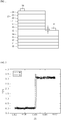
- Fig. 1 is a sectional view of a light emitting device according to an embodiment.
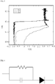
- Figs. 2 and 3 are views illustrating a snap back phenomenon in a light emitting device according to an embodiment.
- Fig. 4 is a view illustrating an operating circuit of a light emitting device according to an embodiment.
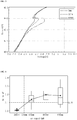
- Fig. 5 is a view illustrating a voltage-current curve according to an etched thickness of an n-type contact layer in a light emitting device according to an embodiment.
- Fig. 6 is a view illustrating a stabilizer voltage deviation according to a thickness of an undoped semiconductor layer 16.
- Fig. 7 is a view of a light emitting device package having a light emitting device applied according to an embodiment.
- Fig. 8 is a view of a lighting apparatus having a light emitting device applied according to an embodiment.
- Figs. 9 and 10 are views of a display device having a light emitting device applied according to an embodiment.
- each layer is exaggerated, omitted, or schematically illustrated for convenience in description and clarity. Also, the size of each element does not entirely reflect an actual size.
- Fig. 1 is a sectional view of a light emitting device according to an embodiment.
- the light emitting device may comprise an n-type semiconductor layer 14, an n-type contact layer 15, a second undoped semiconductor layer 16, an active layer 17, a p-type semiconductor layer 20, a first electrode 18, and a second electrode 19.
- the n-type semiconductor layer 14 may comprise a first area and a second area in a plane.
- the n-type contact layer 15 may be disposed on the n-type semiconductor layer 14, and may have a first thickness in the first area and a second thickness in the second area.
- the second undoped semiconductor layer 16 may be disposed in the first area and also may be disposed on the n-type semiconductor layer 15 having the first thickness.
- the active layer 17 may be disposed in the first area and also may be disposed on the second undoped semiconductor layer 16.
- the p-type layer 20 may be disposed in the first area and also may be disposed on the active layer 17.
- the first electrode 18 may be disposed in the second area and also may be disposed on the n-type contact layer 15 having the second thickness.
- the second electrode 19 may be disposed one the p-type semiconductor layer 20.
- the light emitting device may comprise a substrate 10, a buffer layer 11, a first undoped semiconductor layer 12, and a crystal control layer 13, below the n-type semiconductor layer 14.
- the p-type semiconductor layer 20 may comprise a first semiconductor layer 21, a second semiconductor layer 22, a third semiconductor layer 23, and a fourth semiconductor layer 24.
- the substrate 10 may be formed of at least one of sapphire (Al 2 O 3 ), SiC, Si, GaAs, GaN, ZnO, GaP, InP, and Ge.
- An uneven pattern may be formed on the top surface of the substrate 10. Crystal quality of a semiconductor layer growing on the substrate 10 may be improved by the uneven pattern.
- the buffer layer 11 may be formed on the substrate 10, and may be formed of a Group III-V elements compound semiconductor.
- the first undoped semiconductor layer 12 may be disposed on the buffer layer 11.
- the first undoped semiconductor layer 12 may be formed of an undoped GaN based semiconductor layer.
- the crystal control layer 13 may be disposed on the first undoped semiconductor layer 12.
- the crystal control layer 13 may be formed with an AlGaN/GaN layer stacked structure or a superlattice structure.
- the crystal control layer 13 may suppress crystal defect occurrence caused by lattice mismatching of the substrate 10 and the GaN based semiconductor layer. That is, electric potential generation progressing in a growth direction may be suppressed.
- a semiconductor layer doped with In instead of the first undoped semiconductor layer 12 may be disposed and the present invention is not limited thereto.
- the first undoped semiconductor layer 12 or/and the crystal control layer 13 may not be formed, and this feature may vary within the technical range of an embodiment.
- the n-type semiconductor layer 14 may be formed on the crystal control layer 13, and the n-type contact layer 15 may be formed on the n-type semiconductor layer 14.
- the n-type semiconductor layer 14 and the n-type contact layer 15 may be formed of a Group III-V compound semiconductor doped with an n-type dopant.
- the n-type semiconductor layer 14 and the n-type contact layer 15 may comprise at least one of be formed of GaN, InN, AIN, InGaN, AlGaN, InAlGaN, and AlInN.
- the n-type semiconductor layer 14 and the n-type contact layer 15 may comprise In as a dopant.
- the n-type semiconductor layer 14 and the n-type contact layer 15 may comprise Si as a dopant, and may be formed to have a dopant concentration of more than or equal to 5 ⁇ 10 18 /cm 3 , for example. Moreover, although the n-type semiconductor layer 14 and the n-type contact layer 15 are separated in Fig. 1 , they may be formed of one layer. For example, the n-type semiconductor layer 14 may be formed to serve as the n-type contact layer 15.
- the second undoped semiconductor layer 16 may be disposed in the first area of the n-type contact layer 15, and the first electrode 18 may be disposed in the second area of the n-type contact layer 15.
- the active layer 17 may be disposed on the second undoped semiconductor layer 16.
- the second undoped semiconductor layer 16 is formed in order to improve the crystal quality of the active layer 17 growing thereon.
- the second undoped layer 16 may comprise at least one of be formed of GaN, InN, AIN, InGaN, AlGaN, InAlGaN, and AlInN.
- the second undoped semiconductor layer 16 may be formed with a thickness of 10 nm to 300 nm.
- the active layer 17 may be formed with a single well structure or a multi well structure.
- the active layer 17 may be formed in a period of a well layer and a barrier layer by using compound semiconductor materials of Group III-V elements, for example, in a period of In x Al y Ga (1-x-y) N well layer/In a Al b Ga (1-a-b) N barrier layer (0 ⁇ x ⁇ 1, 0 ⁇ y ⁇ 1, 0 ⁇ x+y ⁇ 1, 0 ⁇ a ⁇ 1, 0 ⁇ b ⁇ 1, 0 ⁇ a+b ⁇ 1).
- a method of growing the active layer 17 supplies nitrogen or/and hydrogen as a carrier gas in a predetermined growth temperature, and selectively supplies NH3, TMGa (or TEGa), TMln, and TMAl in order to alternately grow a well layer and a barrier layer.
- the growth temperatures of the well layer and the barrier layer may be the same or the growth temperature of the barrier layer may be higher than that of the well layer.
- the growth speed of the well layer may be less than 0.2 ⁇ /sec (i.e., slow speed) and the well layer may be thickly grown in 28 ⁇ to 32 ⁇ .
- An In composition in the well layer is at least 10 % for growth, and a single or multi barrier layer may be formed on the well layer.
- One or a plurality of pairs of the well layer/barrier layer may be grown.
- the p-type semiconductor layer 20 may be disposed on the active layer 17.
- the p-type semiconductor layer 20 may be formed of a single layer or a multi layer by using GaN, InN, AIN, InGaN, AlGaN, InAlGaN, and AlInN.
- the p-type semiconductor layer 20 may comprise a p-type dopant such as Mg.
- a p-type buffer layer may be further disposed between the active layer 17 and the p-type semiconductor layer 20.
- the p-type buffer layer may be formed of a Group III-V elements compound semiconductor doped with a p-type dopant such as InAlGaN or AlGaN.
- the p-type buffer layer may not be formed, and the present invention is not limited thereto.
- the p-type semiconductor layer 20 may comprise a first semiconductor layer 21, a second semiconductor layer 22, a third semiconductor layer 23, and a fourth semiconductor layer 24.
- the first semiconductor layer 21 has a first dopant concentration; the second semiconductor layer 22 has a second dopant concentration; the third semiconductor layer 23 has a third dopant concentration; and the fourth semiconductor layer 24 has a fourth dopant concentration.
- the second dopant concentration may have a smaller value than the first and third dopant concentrations, and the fourth dopant concentration may have a larger value than the third dopant concentration.
- the first semiconductor layer 21 may be formed with a p-type dopant concentration of 1 ⁇ 10 20 /cm 3 to 2 ⁇ 10 20 /cm 3 and the second semiconductor layer 22 may be formed with a p-type dopant concentration of less than 1 ⁇ 10 19 /cm 3 .
- the third semiconductor layer 23 is formed to have a p-type dopant concentration of 1 ⁇ 10 2. /cm 3 to 2 ⁇ 10 20 /cm 3
- the fourth semiconductor layer 24 may be formed to have a p-type dopant concentration of more than 2 ⁇ 10 20 /cm 3 in order to lower resistance.
- the p-type dopant concentration in the p-type semiconductor layer 20 has a [P+/P0/P+/P++] form, and satisfies electrical and optical properties that the light emitting device requires.
- the surface of the p-type semiconductor layer 20 is etched to a predetermined depth through an etching process, in order to expose the n-type contact layer 15 and form the first electrode 18 on the exposed n-type contact layer 15.
- the etching process may comprise a dry etching process.
- the predetermined depth from the surface of the p-type semiconductor layer 20 may be 750 nm to 850 nm, for example.
- the n-type contact layer 15 may not be exposed.
- the first electrode 18 may be formed on the second undoped semiconductor layer 16.
- a snap back phenomenon of a current-voltage curve may occur as shown in Figs. 2 and 3 .
- the dotted line in Figs. 2 and 3 represents that a snap back phenomenon occurs, and the solid line represents that a snap back phenomenon does not occur. Since voltage is measured after 1 ms elapses as soon as typical drive current is applied, a general method may not detect a snap back phenomenon. However, if initial voltage is measured using an oscilloscope, a voltage, which is higher by 0.1 V to 3.0 V than typical voltage, is measured, and then, stabilized during a very short initial time of about 0 ⁇ s to about 100 ⁇ s.
- the second undoped semiconductor layer 16 may be disposed in the first area of the n-type contact layer 15, and the first electrode 18 may be disposed in the second area of the n-type contact layer 15.
- Fig. 5 is a view illustrating a voltage-current curve according to an etched thickness of the n-type contact layer 15 in a light emitting device according to an embodiment. Voltage-current curves are shown in Fig. 5 when etched thicknesses of the n-type contact layer 15 are 0 nm, 50 nm, and 100 nm, respectively.
- the etched thickness of the n-type contact layer 15 means a height difference between the first area top surface of the n-type contact layer 15 having the second undoped semiconductor layer 16 and the second area top surface of the n-type contact layer 15 having the first electrode 18.
- a discontinuous voltage-current curve that does not follow Ohm's law is formed when the etched thickness of the n-type contact layer 15 is 0 nm or 50 nm.
- operational malfunction for example, no screen is displayed during initial start-up
- a voltage-current curve that follows Ohm's law is formed when the etched thickness of the n-type contact layer 15 is 100 nm.
- an etched thickness of the n-type contact layer 15 that is, a thickness t of a height difference between the first area of the n-type contact layer 15 having the second undoped semiconductor layer 16 and the second area of the n-type contact layer 15 having the first electrode 18, may be 100 nm to 300 nm.
- the etched depth from the surface of the p-type semiconductor layer 20 may be 800 nm to 1300 nm, for example. That is, a thickness from the top surface of the p-type semiconductor layer 20 to the second area top surface of the n-type contact layer 15 may be 800 nm to 1300 nm.
- Fig. 6 is a view illustrating a stabilizer voltage deviation according to a thickness of the second undoped semiconductor layer 16.
- Delta_VF in the y axis represents a difference between VF raising high at the initial driving and stabilized VF. That is, when the second undoped semiconductor layer 16 is thick, there may be an area where the current-voltage curve does not follow Ohm's law.
- Delta-VF represents the degree of a voltage deviation between a curve interval against ohm's law and a curve following Ohm's law.
- Fig. 6 is a view when an undoped GaN layer is formed as one example of the second undoped semiconductor layer 16.
- Delta_Vf has a value of less than 0.1 V when the thickness of the second undoped semiconductor layer 16 is 300 nm.
- a light emitting device whose a current-voltage curve follows Ohm's law may be realized.
- the second undoped semiconductor layer 16 may be realized to have a thickness of less than or equal to 300 nm.
- the second undoped semiconductor layer 16 may be realized to have a thickness of 10 nm to 300 nm.
- a driving voltage reaches 3.5 V to 8.0 V, which exceeds a normal driving voltage of 2.8 V to 3.4 V due to hunting, for a short time between 0 ⁇ s to 100 ⁇ s during an initial start-up.
- This abnormal driving voltage causes operational malfunction (for example, no screen is displayed in a product such as a notebook computer). However, according to an embodiment, the operational malfunction may be prevented.
- a transparent electrode may be further disposed between the p-type semiconductor layer 20 and the second electrode 19.
- the transparent electrode may comprise at least one of ITO, In-ZnO (IZO), Ga-ZnO (GZO), Al-ZnO (AZO), Al-Ga ZnO (AGZO), In-Ga ZnO (IGZO), IrOx, RuOx, RuOx/ITO, Ni/IrOx/Au, and Ni/IrOx/Au/ITO, but is not limited thereto.
- Fig. 7 is a view of a light emitting device package having a light emitting device applied according to an embodiment.
- the light emitting device package comprises a main body unit 200, a first electrode layer 210 and a second electrode layer 220 in the main body unit 200, a light emitting device 100 installed at the main body unit 200 and electrically connected to the first electrode layer 210 and the second electrode layer 220, and a molding member 400 surrounding the light emitting device 100.
- the main body unit 200 may be formed of silicon material, synthetic resin material, or metal material, and an inclined plane may be formed around the light emitting device 100.
- the first electrode layer 210 and the second electrode layer 220 are electrically separated from each other, and serve to provide power to the light emitting device 100. Additionally, the first electrode layer 210 and the second electrode layer 220 may serve to increase light efficiency by reflecting the light generated from the light emitting device 100, and may also serve to exhaust the heat generated from the light emitting device 100 to the external.
- the light emitting device 100 may be applied to the light emitting devices according to the above described embodiments, and may be disposed on the main body unit 200 or the first electrode layer 210 or the second electrode layer 220.
- the light emitting device 100 may be electrically connected to the first electrode layer 210 and/or the second electrode layer 220 through a wire 300.
- a wire 300 since the light emitting device 100 having a vertical type is exemplarily shown, one wire 300 is used.
- two wires 300 may be used.
- no wire when the light emitting device 100 has a flip chip type, no wire may be used.
- the molding member 400 may surround the light emitting device 100 to protect it. Additionally, since the molding member 400 comprises a fluorescent substance, it may change the wavelength of light emitted from the light emitting device 100.
- Fig. 8 is a view of a lighting apparatus having a light emitting device applied according to an embodiment.
- the lighting apparatus 1200 of Fig. 8 is just one example of a lighting system, and the present invention is not limited thereto.
- the lighting apparatus 1200 may comprise a case main body 1210, a light emitting module 1230 at the case main body 1210, and a connection terminal 1220 at the case main body 1210 to receive power from an external power supply unit.
- the case main body 1210 may be formed of a material having excellent heat dissipation characteristic, for example, metal material or resin material.
- the light emitting module 1230 may comprise a board 1233 and a light emitting device 1231 mounted on the board according to at least one embodiment.
- the board 1233 may be formed with a circuit pattern printed on an insulator, and may comprise a typical Printed Circuit Board (PCB), a metal core PCB, a flexible PCB, and a ceramic PCB.
- PCB Printed Circuit Board
- the board 1233 may be formed of a material that efficiently reflects light or may have the surface whose color efficiently reflects light such as white or silver.
- the light emitting device 1231 may be disposed on the board 1233.
- the light emitting device 1231 may comprise at least one Light Emitting Diode (LED).
- the light emitting diode may comprise a colored LED emitting each colored light of red, green, blue or white, and an UltraViolet (UV) LED emitting UV
- the light emitting module 1230 may be disposed to have various LED combinations to obtain color and brightness. For example, in order to obtain a high Color Rendering Index (CRI), a white LED, a red LED, and a green LED may be combined and disposed. Additionally, a fluorescent sheet may be further disposed on a propagation path of light emitted from the light emitting module 1230, and may change the wavelength of light emitted from the light emitting module 1230. For example, if the light emitted from the light emitting module 1230 has a blue wavelength range, the fluorescent sheet may comprise a yellow fluorescent substance. The light emitted from the light emitting module 1230 passes through the fluorescent sheet, and then, finally is displayed as white light.
- CRI Color Rendering Index
- connection terminal 1220 is electrically connected to the light emitting module 1230 so that power may be supplied to the light emitting module 1230 through the connection terminal 1220.
- the connection terminal 1220 is screwed into and coupled to an external power in a socket type, but is not limited thereto.
- the connection terminal 1220 having a pin may be inserted into an external power or may be connected to an external power through wiring.
- At least one of a light guide member, a diffusion sheet, a light condensing sheet, and a brightness enhancing sheet, and a fluorescent sheet is disposed on a propagation path of light emitted from the light emitting module, so that desired optical effects may be obtained.
- the above light emitting device or light emitting device package may be applied to a display device such as a television and an electronic display board.
- the display device 1000 may comprise a light guide plate 1041, a light emitting module 1031 providing light to the light guide plate 1041, a reflective member 1022 below the light guide plate 1041, an optical sheet 1051 on the light guide plate 1041, a display panel 1061 on the optical sheet 1051, and a bottom cover 1011 receiving the light guide plate 1041, the light emitting module 1031, and the reflective member 1022, but is not limited thereto.
- the bottom cover 1011, the reflective sheet 1022, the light guide plate 1041, and the optical sheet 1051 may be defined as a light unit 1050.
- the light guide plate 1041 may serve as a plane light source by diffusing light.
- the light guide plate 1041 may be formed of a transparent material, and may comprise one of an acrylic resin base such as polymethyl metaacrylate (PMMA), and polyethylene terephthlate (PET), poly carbonate (PC), cycloolefin copolymer (COC) and polyethylene naphthalate (PEN) resins.
- PMMA polymethyl metaacrylate
- PET polyethylene terephthlate
- PC poly carbonate
- COC cycloolefin copolymer
- PEN polyethylene naphthalate
- the light emitting module 1031 provides light to at least one lateral side of the light guide plate 1041, and ultimately serves as a light source of a display device.
- At least one light emitting module 1031 may be provided, and directly or indirectly may provide one lateral side of the light guide plate 1041.
- the light emitting module 1031 may comprise a board 1033 and the light emitting device or the light emitting device package 700 according to the above embodiment.
- the light emitting device package 700 may be arrayed on the board 1033 in a predetermined interval.
- the board may be a PCB comprising a circuit pattern.
- the board 1033 may comprise a Metal Core PCB (MCPCB) and a Flexible PCB (FPCB) in addition to a typical PCB, but is not limited thereto.
- MCPCB Metal Core PCB
- FPCB Flexible PCB
- a light emitting surface that emits light may be mounted spaced a predetermined distance from the light guide plate 1041, but is not limited thereto.
- the light emitting device package 700 may directly or indirectly provide light to a light incident part, i.e., one lateral side of the light guide plate 1041, but is not limited thereto.
- the reflective member 1022 may be disposed below the light guide plate 1041.
- the reflective member 1022 may improve the brightness of the light unit 1050 by reflecting light incident to the bottom side of the light guide plate 1041 toward the upper direction.
- the reflective member 1022 may be formed of PET, PC, and PVC resins but is not limited thereto.
- the reflective member 1022 may be the top surface of the bottom cover 1011 but is not limited thereto.
- the bottom cover 1011 may receive the light guide plate 1041, the light emitting module 1031, and the reflective sheet 1022.
- the bottom cover 1011 may comprise a receiving part 1012 having a box form whose top surface is opened, but is not limited thereto.
- the bottom cover 1011 may be coupled to a top cover, but is not limited thereto.
- the bottom cover 1011 may be formed of a metal material or a resin material, and may be manufactured through a process such as press molding or extrusion molding. Additionally, the bottom cover 1011 may comprise a metallic or nonmetallic material having excellent thermal conductivity, but is not limited thereto.
- the display panel 1061 may be a Liquid Crystal Display (LCD) panel, and may comprise transparent first and second substrates facing each other and a liquid crystal layer interposed between the first and second substrates.
- a polarizing plate may be attached to at least one side of the display panel 1061, but is not limited thereto.
- the display panel 1061 displays information through the light passing through the optical sheet 1051.
- the display device 1000 may be applied to the displays of various portable terminals and a notebook computer, and the monitor of a television.
- the optical sheet 1051 is disposed between the display panel 1061 and the light guide plate 1041, and comprises at least one transparent sheet.
- the optical sheet 1051 may comprise at least one of a diffusion sheet, a parallel and/or vertical prism sheet, and a brightness enhancing sheet.
- the diffusion sheet diffuses incident light; the parallel and/or vertical prism sheet condenses incident light in a display area; and the brightness enhancing sheet reuses losing light to improve brightness.
- a protective sheet may be disposed on the display panel 1061, but is not limited thereto.
- the light guide plate 1041 and the optical sheet 1051 as an optical member may be disposed on a light propagation path of the light emitting module 1031, but are not limited thereto.
- Fig. 10 is a view of a display device according to another embodiment.
- the display device 1100 comprises a bottom cover 1152, a board 1020 where the above light emitting device or light emitting device package 700 is arrayed, an optical member 1154, and a display panel 1155.
- the board 1020 and the light emitting device package 700 may be defined as a light emitting module 1060.
- the bottom cover 1152, at least one light emitting module 1060, and the optical member 1154 may be defined as a light unit.
- the bottom cover 1152 may comprise a receiving part 1153, but is not limited thereto.
- the optical member 1154 may comprise at least one of a lens, a light guide plate, a diffusion sheet, a parallel and/or vertical prism sheet, and a brightness enhancing sheet.
- the light guide plate may be formed of a PC material or a PMMA material, and may be removed.
- the diffusion sheet diffuses incident light; the parallel and/or vertical prism sheet condenses incident light in a display area; and the brightness enhancing sheet reuses losing light to improve brightness.
- the optical member 1154 is disposed on the light emitting module 1060, and thus may use the light emitted from the light emitting module 1060 as a plane light source, or diffuse or condense the light.
- a light emitting device a light emitting device package, and a lighting apparatus, which have a new structure, may be provided.
- a light emitting device a light emitting device package, and a lighting apparatus, which reduce crystal defects and improve brightness and driving characteristics, may be provided.
Landscapes
- Led Devices (AREA)
Abstract
Description
- The present disclosure relates to a light emitting device, a light emitting device package, and a lighting apparatus.
- A Light Emitting Diode (LED) is typically used as a light emitting device. The LED converts electrical signals into the form of light such as infrared or visible rays by using characteristics of a compound semiconductor.
- As light efficiency of a light emitting device is increased, it is used for various electrical and electronic devices such as a display device and a lighting device.
- Embodiments provide a light emitting device, a light emitting device package, and a lighting apparatus, which have a new structure.
- Embodiments also provide a light emitting device, a light emitting device package, and a lighting apparatus, which reduce crystal defects and improve brightness and driving characteristics.
- In one embodiment, a light emitting device comprises: an n-type semiconductor layer comprising a first area and a second area in a plane; an n-type contact layer disposed on the n-type semiconductor layer and has a first thickness in the first area and a second thickness in the second area; an undoped semiconductor layer disposed on the n-type contact layer having the first thickness in the first area; an active layer disposed on the undoped semiconductor layer in the first area; a p-type semiconductor layer disposed on the active layer in the first area; a first electrode disposed on the n-type contact layer having the second thickness in the second area; and a second electrode disposed on the p-type semiconductor layer, wherein the undoped semiconductor layer has a thickness of less than or equal to 300 nm; and a height difference between the top surface of the n-type contact layer in the first area and the top surface of the n-type contact layer in the second area is at least 100 nm.
- In another embodiment, a light emitting device comprises: an n-type semiconductor layer comprising an an-type contact layer; an undoped semiconductor layer in a first area of the n-type contact layer; an active layer on the undoped semiconductor layer; a p-type semiconductor layer on the active layer; a first electrode in a second area of the n-type contact layer; and a second electrode on the p-type semiconductor layer, wherein the undoped semiconductor layer has a thickness of less than or equal to 300 nm, and a height difference between the first area of the n-type contact layer having the undoped semiconductor layer thereon and the second area of the n-type contact layer having the first electrode thereon is at least 100 nm.
- In further another embodiment, a lighting emitting device package comprises: a case main body; a light emitting module disposed at the case main body and comprising a light emitting device; and a connection terminal disposed at the case main body and receiving power from a external power supply, wherein the light emitting device comprises: an n-type semiconductor layer comprising a first area and a second area in a plane; an n-type contact layer disposed on the n-type semiconductor layer and has a first thickness in the first area and a second thickness in the second area; an undoped semiconductor layer disposed on the n-type contact layer having the first thickness in the first area; an active layer disposed on the undoped semiconductor layer in the first area; a p-type semiconductor layer disposed on the active layer in the first area; a first electrode disposed on the n-type contact layer having the second thickness in the second area; and a second electrode disposed on the p-type semiconductor layer, wherein the undoped semiconductor layer has a thickness of less than or equal to 300 nm; and a height difference between the top surface of the n-type contact layer in the first area and the top surface of the n-type contact layer in the second area is at least 100 nm.
- In still further another embodiment, a light emitting device package comprises: a case main body; a light emitting module disposed at the case main body and comprising a light emitting device; and a connection terminal disposed at the case main body and receiving power from a external power supply, wherein the light emitting device comprises: an n-type semiconductor layer comprising a first area and a second area in a plane; an n-type contact layer disposed on the n-type semiconductor layer and has a first thickness in the first area and a second thickness in the second area; an undoped semiconductor layer disposed on the n-type contact layer having the first thickness in the first area; an active layer disposed on the undoped semiconductor layer in the first area; a p-type semiconductor layer disposed on the active layer in the first area; a first electrode disposed on the n-type contact layer having the second thickness in the second area; and a second electrode disposed on the p-type semiconductor layer, wherein the undoped semiconductor layer has a thickness of less than or equal to 300 nm; and a height difference between the top surface of the n-type contact layer in the first area and the top surface of the n-type contact layer in the second area is at least 100 nm.
- In still further another embodiment, a lighting apparatus comprises: a case main body; a light emitting module disposed at the case main body and comprising a light emitting device; and a connection terminal disposed at the case main body and receiving power from a external power supply, wherein the light emitting device comprises: an n-type semiconductor layer comprising a first area and a second area in a plane; an n-type contact layer disposed on the n-type semiconductor layer and has a first thickness in the first area and a second thickness in the second area; an undoped semiconductor layer disposed on the n-type contact layer having the first thickness in the first area; an active layer disposed on the undoped semiconductor layer in the first area; a p-type semiconductor layer disposed on the active layer in the first area; a first electrode disposed on the n-type contact layer having the second thickness in the second area; and a second electrode disposed on the p-type semiconductor layer, wherein the undoped semiconductor layer has a thickness of less than or equal to 300 nm; and a height difference between the top surface of the n-type contact layer in the first area and the top surface of the n-type contact layer in the second area is at least 100 nm.
- In still further another embodiment, a lighting apparatus comprises: a case main body; a light emitting module disposed at the case main body and comprising a light emitting device; and a connection terminal disposed at the case main body and receiving power from a external power supply, wherein the light emitting device comprises: an n-type semiconductor layer comprising an an-type contact layer; an undoped semiconductor layer in a first area of the n-type contact layer; an active layer on the undoped semiconductor layer; a p-type semiconductor layer on the active layer; a first electrode in a second area of the n-type contact layer; and a second electrode on the p-type semiconductor layer, wherein the undoped semiconductor layer has a thickness of less than or equal to 300 nm, and a height difference between the first area of the n-type contact layer having the undoped semiconductor layer thereon and the second area of the n-type contact layer having the first electrode thereon is at least 100 nm.
- A difference between the first thickness of the n-type contact layer and the second thickness thereof may be at least 100 nm.
- The undoped semiconductor layer may be formed of at least one of GaN, InN, AIN, InGaN, AlGaN, InAlGaN, and AlInN.
- The undoped semiconductor layer may have a thickness of 10 nm to 300 nm.
- The p-type semiconductor layer may comprise a first semiconductor layer having a first dopant concentration, a second semiconductor layer having a second dopant concentration, a third semiconductor layer having a third dopant concentration, and a fourth semiconductor layer having a fourth dopant concentration; the second dopant concentration may have a smaller value than the first dopant concentration and the third dopant concentration; and the fourth dopant concentration may have a greater value than the third dopant concentration.
- The first semiconductor layer has a dopant concentration of 1 × 10²⁰/cm3 to 2×10²⁰/cm3; the second semiconductor layer has a dopant concentration of less than or equal to 1×10¹⁹/cm3; and the third semiconductor layer has a dopant concentration of 1×10²⁰/cm3 to 2×10²⁰/cm3.
- The light emitting device may further comprise a transparent electrode between the p-type semiconductor layer and the second electrode.
- The transparent electrode may comprise at least one of ITO, In-ZnO (IZO), Ga-ZnO (GZO), Al-ZnO (AZO), Al-Ga ZnO (AGZO), In-Ga ZnO (IGZO), IrOx, RuOx, RuOx/ITO, Ni/IrOx/Au, and Ni/IrOx/Au/ITO.
- The first electrode may contact the n-type contact layer.
- A thickness from the top surface of the p-type semiconductor layer to the top surface of the n-type contact layer in the second area may be 800 nm to 1300 nm.
- The light emitting device may further comprise a substrate below the n-type semiconductor layer.
- The light emitting device may further comprise an uneven pattern on the top surface of the substrate.
- The light emitting device may further comprise a buffer layer and a crystal control layer on the substrate.
- The n-type contact layer comprises at least one of GaN, InN, AIN, InGaN, AlGaN, InAlGaN, and AlInN.
- The n-type contact layer may comprise In or Si as a dopant.
- The details of one or more embodiments are set forth in the accompanying drawings and the description below. Other features will be apparent from the description and drawings, and from the claims.
-
Fig. 1 is a sectional view of a light emitting device according to an embodiment. -
Figs. 2 and3 are views illustrating a snap back phenomenon in a light emitting device according to an embodiment. -
Fig. 4 is a view illustrating an operating circuit of a light emitting device according to an embodiment. -
Fig. 5 is a view illustrating a voltage-current curve according to an etched thickness of an n-type contact layer in a light emitting device according to an embodiment. -
Fig. 6 is a view illustrating a stabilizer voltage deviation according to a thickness of anundoped semiconductor layer 16. -
Fig. 7 is a view of a light emitting device package having a light emitting device applied according to an embodiment. -
Fig. 8 is a view of a lighting apparatus having a light emitting device applied according to an embodiment. -
Figs. 9 and 10 are views of a display device having a light emitting device applied according to an embodiment. - In the description of embodiments, it will be understood that when a layer (or film), region, pattern or structure is referred to as being 'on' or 'under' another layer (or film), region, pad or pattern, the terminology of 'on' and 'under' comprises both the meanings of 'directly' and 'indirectly'. Further, the reference about 'on' and 'under' each layer will be made on the basis of drawings.
- In the drawings, the thickness or size of each layer is exaggerated, omitted, or schematically illustrated for convenience in description and clarity. Also, the size of each element does not entirely reflect an actual size.
- Hereinafter, a light emitting device and a light emitting device package according to embodiments will be described with reference to the accompanying drawings.
-
Fig. 1 is a sectional view of a light emitting device according to an embodiment. - The light emitting device may comprise an n-
type semiconductor layer 14, an n-type contact layer 15, a secondundoped semiconductor layer 16, anactive layer 17, a p-type semiconductor layer 20, afirst electrode 18, and asecond electrode 19. - The n-
type semiconductor layer 14 may comprise a first area and a second area in a plane. The n-type contact layer 15 may be disposed on the n-type semiconductor layer 14, and may have a first thickness in the first area and a second thickness in the second area. The secondundoped semiconductor layer 16 may be disposed in the first area and also may be disposed on the n-type semiconductor layer 15 having the first thickness. Theactive layer 17 may be disposed in the first area and also may be disposed on the secondundoped semiconductor layer 16. The p-type layer 20 may be disposed in the first area and also may be disposed on theactive layer 17. Thefirst electrode 18 may be disposed in the second area and also may be disposed on the n-type contact layer 15 having the second thickness. Thesecond electrode 19 may be disposed one the p-type semiconductor layer 20. - The light emitting device may comprise a
substrate 10, abuffer layer 11, a firstundoped semiconductor layer 12, and acrystal control layer 13, below the n-type semiconductor layer 14. The p-type semiconductor layer 20 may comprise afirst semiconductor layer 21, asecond semiconductor layer 22, athird semiconductor layer 23, and afourth semiconductor layer 24. - The
substrate 10 may be formed of at least one of sapphire (Al2O3), SiC, Si, GaAs, GaN, ZnO, GaP, InP, and Ge. An uneven pattern may be formed on the top surface of thesubstrate 10. Crystal quality of a semiconductor layer growing on thesubstrate 10 may be improved by the uneven pattern. Thebuffer layer 11 may be formed on thesubstrate 10, and may be formed of a Group III-V elements compound semiconductor. The firstundoped semiconductor layer 12 may be disposed on thebuffer layer 11. For example, the firstundoped semiconductor layer 12 may be formed of an undoped GaN based semiconductor layer. - The
crystal control layer 13 may be disposed on the firstundoped semiconductor layer 12. Thecrystal control layer 13 may be formed with an AlGaN/GaN layer stacked structure or a superlattice structure. Thecrystal control layer 13 may suppress crystal defect occurrence caused by lattice mismatching of thesubstrate 10 and the GaN based semiconductor layer. That is, electric potential generation progressing in a growth direction may be suppressed. Moreover, a semiconductor layer doped with In instead of the firstundoped semiconductor layer 12 may be disposed and the present invention is not limited thereto. The firstundoped semiconductor layer 12 or/and thecrystal control layer 13 may not be formed, and this feature may vary within the technical range of an embodiment. - The n-
type semiconductor layer 14 may be formed on thecrystal control layer 13, and the n-type contact layer 15 may be formed on the n-type semiconductor layer 14. The n-type semiconductor layer 14 and the n-type contact layer 15 may be formed of a Group III-V compound semiconductor doped with an n-type dopant. For example, the n-type semiconductor layer 14 and the n-type contact layer 15 may comprise at least one of be formed of GaN, InN, AIN, InGaN, AlGaN, InAlGaN, and AlInN. The n-type semiconductor layer 14 and the n-type contact layer 15 may comprise In as a dopant. The n-type semiconductor layer 14 and the n-type contact layer 15 may comprise Si as a dopant, and may be formed to have a dopant concentration of more than or equal to 5×10¹⁸/cm3, for example. Moreover, although the n-type semiconductor layer 14 and the n-type contact layer 15 are separated inFig. 1 , they may be formed of one layer. For example, the n-type semiconductor layer 14 may be formed to serve as the n-type contact layer 15. - The second
undoped semiconductor layer 16 may be disposed in the first area of the n-type contact layer 15, and thefirst electrode 18 may be disposed in the second area of the n-type contact layer 15. Theactive layer 17 may be disposed on the secondundoped semiconductor layer 16. - The second
undoped semiconductor layer 16 is formed in order to improve the crystal quality of theactive layer 17 growing thereon. For example, the secondundoped layer 16 may comprise at least one of be formed of GaN, InN, AIN, InGaN, AlGaN, InAlGaN, and AlInN. The secondundoped semiconductor layer 16 may be formed with a thickness of 10 nm to 300 nm. - The
active layer 17 may be formed with a single well structure or a multi well structure. Theactive layer 17 may be formed in a period of a well layer and a barrier layer by using compound semiconductor materials of Group III-V elements, for example, in a period of InxAlyGa(1-x-y)N well layer/InaAlbGa(1-a-b)N barrier layer (0<x≤1, 0≤y≤1, 0≤x+y≤1, 0≤a≤1, 0≤b≤1, 0≤a+b≤1). - A method of growing the
active layer 17 supplies nitrogen or/and hydrogen as a carrier gas in a predetermined growth temperature, and selectively supplies NH3, TMGa (or TEGa), TMln, and TMAl in order to alternately grow a well layer and a barrier layer. The growth temperatures of the well layer and the barrier layer may be the same or the growth temperature of the barrier layer may be higher than that of the well layer. - At this pint, the growth speed of the well layer may be less than 0.2□/sec (i.e., slow speed) and the well layer may be thickly grown in 28□ to 32□. An In composition in the well layer is at least 10 % for growth, and a single or multi barrier layer may be formed on the well layer. One or a plurality of pairs of the well layer/barrier layer may be grown.
- The p-
type semiconductor layer 20 may be disposed on theactive layer 17. For example, the p-type semiconductor layer 20 may be formed of a single layer or a multi layer by using GaN, InN, AIN, InGaN, AlGaN, InAlGaN, and AlInN. The p-type semiconductor layer 20 may comprise a p-type dopant such as Mg. A p-type buffer layer may be further disposed between theactive layer 17 and the p-type semiconductor layer 20. The p-type buffer layer may be formed of a Group III-V elements compound semiconductor doped with a p-type dopant such as InAlGaN or AlGaN. The p-type buffer layer may not be formed, and the present invention is not limited thereto. - According to the light emitting device, the p-
type semiconductor layer 20 may comprise afirst semiconductor layer 21, asecond semiconductor layer 22, athird semiconductor layer 23, and afourth semiconductor layer 24. Thefirst semiconductor layer 21 has a first dopant concentration; thesecond semiconductor layer 22 has a second dopant concentration; thethird semiconductor layer 23 has a third dopant concentration; and thefourth semiconductor layer 24 has a fourth dopant concentration. - The second dopant concentration may have a smaller value than the first and third dopant concentrations, and the fourth dopant concentration may have a larger value than the third dopant concentration.
- For example, when a 2 inch growth substrate is used, in order to obtain an Electro Static Discharge (ESD) tolerance, the
first semiconductor layer 21 may be formed with a p-type dopant concentration of 1×10²⁰/cm3 to 2×10²⁰/cm3 and thesecond semiconductor layer 22 may be formed with a p-type dopant concentration of less than 1×10¹⁹/cm3. Additionally, thethird semiconductor layer 23 is formed to have a p-type dopant concentration of 1×10²./cm3 to 2×10²⁰/cm3, and thefourth semiconductor layer 24 may be formed to have a p-type dopant concentration of more than 2×10²⁰/cm3 in order to lower resistance. The p-type dopant concentration in the p-type semiconductor layer 20 has a [P+/P0/P+/P++] form, and satisfies electrical and optical properties that the light emitting device requires. - Additionally, in relation to a method of manufacturing a light emitting device, the surface of the p-
type semiconductor layer 20 is etched to a predetermined depth through an etching process, in order to expose the n-type contact layer 15 and form thefirst electrode 18 on the exposed n-type contact layer 15. The etching process may comprise a dry etching process. At this point, the predetermined depth from the surface of the p-type semiconductor layer 20 may be 750 nm to 850 nm, for example. - However, when the second
undoped semiconductor layer 16 is too thick or the etched thickness is too thin during the etching process, the n-type contact layer 15 may not be exposed. Like this, when the n-type contact layer 15 is not exposed, thefirst electrode 18 may be formed on the secondundoped semiconductor layer 16. - When the
first electrode 18 is formed on the secondundoped semiconductor layer 16, a snap back phenomenon of a current-voltage curve may occur as shown inFigs. 2 and3 . The dotted line inFigs. 2 and3 represents that a snap back phenomenon occurs, and the solid line represents that a snap back phenomenon does not occur. Since voltage is measured after 1 ms elapses as soon as typical drive current is applied, a general method may not detect a snap back phenomenon. However, if initial voltage is measured using an oscilloscope, a voltage, which is higher by 0.1 V to 3.0 V than typical voltage, is measured, and then, stabilized during a very short initial time of about 0 µs to about 100 µs. - It is analyzed that this is because electrons injected from the
first electrode 18 are not smoothly propagated and are collected due to the secondundoped semiconductor layer 16, thereby causing a kind of a capacitor phenomenon. This allows to be interpreted as shown inFig. 4 in terms of a circuit. - In consideration of the above fact, suggested is a method of disposing the
first electrode 18 on the n-type contact layer 15 in the light emitting device in order to prevent a snap back phenomenon. Additionally, in relation to a suggested method according to an embodiment, the secondundoped semiconductor layer 16 may be disposed in the first area of the n-type contact layer 15, and thefirst electrode 18 may be disposed in the second area of the n-type contact layer 15. Moreover, in relation to a suggested method according to an embodiment, there may be a height difference between the first area and the second area of the n-type contact layer 15 in the light emitting device. -
Fig. 5 is a view illustrating a voltage-current curve according to an etched thickness of the n-type contact layer 15 in a light emitting device according to an embodiment. Voltage-current curves are shown inFig. 5 when etched thicknesses of the n-type contact layer 15 are 0 nm, 50 nm, and 100 nm, respectively. Here, the etched thickness of the n-type contact layer 15 means a height difference between the first area top surface of the n-type contact layer 15 having the secondundoped semiconductor layer 16 and the second area top surface of the n-type contact layer 15 having thefirst electrode 18. - As shown in
Fig. 5 , a discontinuous voltage-current curve that does not follow Ohm's law is formed when the etched thickness of the n-type contact layer 15 is 0 nm or 50 nm. When a light emitting device having the discontinuous current-voltage characteristic that does not follow ohm's law is applied to a product requiring initial operating characteristics such as a notebook computer, operational malfunction (for example, no screen is displayed during initial start-up) may occur. - However, as shown in
Fig. 5 , a voltage-current curve that follows Ohm's law is formed when the etched thickness of the n-type contact layer 15 is 100 nm. In relation to the light emitting device, since an etched thickness of the n-type contact layer 15 is more than or equal to 100 nm, operational malfunction (for example, no screen is displayed during initial start-up) may be prevented. As an example, Here, an etched thickness of the n-type contact layer 15, that is, a thickness t of a height difference between the first area of the n-type contact layer 15 having the secondundoped semiconductor layer 16 and the second area of the n-type contact layer 15 having thefirst electrode 18, may be 100 nm to 300 nm. At this point, the etched depth from the surface of the p-type semiconductor layer 20 may be 800 nm to 1300 nm, for example. That is, a thickness from the top surface of the p-type semiconductor layer 20 to the second area top surface of the n-type contact layer 15 may be 800 nm to 1300 nm. - Moreover,
Fig. 6 is a view illustrating a stabilizer voltage deviation according to a thickness of the secondundoped semiconductor layer 16. Here, Delta_VF in the y axis represents a difference between VF raising high at the initial driving and stabilized VF. That is, when the secondundoped semiconductor layer 16 is thick, there may be an area where the current-voltage curve does not follow Ohm's law. Delta-VF represents the degree of a voltage deviation between a curve interval against ohm's law and a curve following Ohm's law. Moreover,Fig. 6 is a view when an undoped GaN layer is formed as one example of the secondundoped semiconductor layer 16. - As shown in
Fig. 6 , Delta_Vf has a value of less than 0.1 V when the thickness of the secondundoped semiconductor layer 16 is 300 nm. By controlling a thickness of the secondundoped semiconductor layer 16 on the basis of the data, a light emitting device whose a current-voltage curve follows Ohm's law may be realized. In relation to the light emitting device, the secondundoped semiconductor layer 16 may be realized to have a thickness of less than or equal to 300 nm. Moreover, in relation to the light emitting device, the secondundoped semiconductor layer 16 may be realized to have a thickness of 10 nm to 300 nm. - By controlling an etched thickness of each of the second
undoped semiconductor layer 16 and the n-type contact layer 15, a light emitting device whose a current-voltage curve follows Ohm's law may be realized. Accordingly, when the light emitting device is applied to a product requiring initial operating characteristics such as a notebook computer, operational malfunction may be prevented. - That is, electrons, which injected when a light emitting device is driven, are gathered for a predetermined time and smoothly injected without discharge due to a capacitor in an internal circuit. Thus, a snap back phenomenon occurring when a light emitting device is driven may be prevented. Additionally, a driving voltage reaches 3.5 V to 8.0 V, which exceeds a normal driving voltage of 2.8 V to 3.4 V due to hunting, for a short time between 0 µs to 100 µs during an initial start-up. This abnormal driving voltage causes operational malfunction (for example, no screen is displayed in a product such as a notebook computer). However, according to an embodiment, the operational malfunction may be prevented.
- Moreover, a transparent electrode may be further disposed between the p-
type semiconductor layer 20 and thesecond electrode 19. The transparent electrode may comprise at least one of ITO, In-ZnO (IZO), Ga-ZnO (GZO), Al-ZnO (AZO), Al-Ga ZnO (AGZO), In-Ga ZnO (IGZO), IrOx, RuOx, RuOx/ITO, Ni/IrOx/Au, and Ni/IrOx/Au/ITO, but is not limited thereto. -
Fig. 7 is a view of a light emitting device package having a light emitting device applied according to an embodiment. - Referring to
Fig. 7 , the light emitting device package comprises amain body unit 200, afirst electrode layer 210 and asecond electrode layer 220 in themain body unit 200, alight emitting device 100 installed at themain body unit 200 and electrically connected to thefirst electrode layer 210 and thesecond electrode layer 220, and amolding member 400 surrounding thelight emitting device 100. - The
main body unit 200 may be formed of silicon material, synthetic resin material, or metal material, and an inclined plane may be formed around thelight emitting device 100. - The
first electrode layer 210 and thesecond electrode layer 220 are electrically separated from each other, and serve to provide power to thelight emitting device 100. Additionally, thefirst electrode layer 210 and thesecond electrode layer 220 may serve to increase light efficiency by reflecting the light generated from thelight emitting device 100, and may also serve to exhaust the heat generated from thelight emitting device 100 to the external. - The
light emitting device 100 may be applied to the light emitting devices according to the above described embodiments, and may be disposed on themain body unit 200 or thefirst electrode layer 210 or thesecond electrode layer 220. - The
light emitting device 100 may be electrically connected to thefirst electrode layer 210 and/or thesecond electrode layer 220 through awire 300. According to the embodiment, since thelight emitting device 100 having a vertical type is exemplarily shown, onewire 300 is used. As another example, when thelight emitting device 100 has a parallel type, twowires 300 may be used. Moreover, when thelight emitting device 100 has a flip chip type, no wire may be used. - The
molding member 400 may surround thelight emitting device 100 to protect it. Additionally, since themolding member 400 comprises a fluorescent substance, it may change the wavelength of light emitted from thelight emitting device 100. -
Fig. 8 is a view of a lighting apparatus having a light emitting device applied according to an embodiment. However, thelighting apparatus 1200 ofFig. 8 is just one example of a lighting system, and the present invention is not limited thereto. - Referring to
Fig. 8 , thelighting apparatus 1200 may comprise a casemain body 1210, alight emitting module 1230 at the casemain body 1210, and aconnection terminal 1220 at the casemain body 1210 to receive power from an external power supply unit. - The case
main body 1210 may be formed of a material having excellent heat dissipation characteristic, for example, metal material or resin material. - The
light emitting module 1230 may comprise aboard 1233 and a light emitting device 1231 mounted on the board according to at least one embodiment. - The
board 1233 may be formed with a circuit pattern printed on an insulator, and may comprise a typical Printed Circuit Board (PCB), a metal core PCB, a flexible PCB, and a ceramic PCB. - Additionally, the
board 1233 may be formed of a material that efficiently reflects light or may have the surface whose color efficiently reflects light such as white or silver. - The light emitting device 1231 according to at least one embodiment may be disposed on the
board 1233. The light emitting device 1231 may comprise at least one Light Emitting Diode (LED). The light emitting diode may comprise a colored LED emitting each colored light of red, green, blue or white, and an UltraViolet (UV) LED emitting UV - The
light emitting module 1230 may be disposed to have various LED combinations to obtain color and brightness. For example, in order to obtain a high Color Rendering Index (CRI), a white LED, a red LED, and a green LED may be combined and disposed. Additionally, a fluorescent sheet may be further disposed on a propagation path of light emitted from thelight emitting module 1230, and may change the wavelength of light emitted from thelight emitting module 1230. For example, if the light emitted from thelight emitting module 1230 has a blue wavelength range, the fluorescent sheet may comprise a yellow fluorescent substance. The light emitted from thelight emitting module 1230 passes through the fluorescent sheet, and then, finally is displayed as white light. - The
connection terminal 1220 is electrically connected to thelight emitting module 1230 so that power may be supplied to thelight emitting module 1230 through theconnection terminal 1220. As shown inFig. 8 , theconnection terminal 1220 is screwed into and coupled to an external power in a socket type, but is not limited thereto. For example, theconnection terminal 1220 having a pin may be inserted into an external power or may be connected to an external power through wiring. - In relation to the above-mentioned lighting apparatus, at least one of a light guide member, a diffusion sheet, a light condensing sheet, and a brightness enhancing sheet, and a fluorescent sheet is disposed on a propagation path of light emitted from the light emitting module, so that desired optical effects may be obtained.
- Moreover, the above light emitting device or light emitting device package may be applied to a display device such as a television and an electronic display board.
- Referring to
Fig. 9 , thedisplay device 1000 may comprise alight guide plate 1041, alight emitting module 1031 providing light to thelight guide plate 1041, areflective member 1022 below thelight guide plate 1041, anoptical sheet 1051 on thelight guide plate 1041, adisplay panel 1061 on theoptical sheet 1051, and abottom cover 1011 receiving thelight guide plate 1041, thelight emitting module 1031, and thereflective member 1022, but is not limited thereto. - The
bottom cover 1011, thereflective sheet 1022, thelight guide plate 1041, and theoptical sheet 1051 may be defined as alight unit 1050. - The
light guide plate 1041 may serve as a plane light source by diffusing light. Thelight guide plate 1041 may be formed of a transparent material, and may comprise one of an acrylic resin base such as polymethyl metaacrylate (PMMA), and polyethylene terephthlate (PET), poly carbonate (PC), cycloolefin copolymer (COC) and polyethylene naphthalate (PEN) resins. - The
light emitting module 1031 provides light to at least one lateral side of thelight guide plate 1041, and ultimately serves as a light source of a display device. - At least one light emitting
module 1031 may be provided, and directly or indirectly may provide one lateral side of thelight guide plate 1041. Thelight emitting module 1031 may comprise aboard 1033 and the light emitting device or the light emittingdevice package 700 according to the above embodiment. The light emittingdevice package 700 may be arrayed on theboard 1033 in a predetermined interval. - The board may be a PCB comprising a circuit pattern. However, the
board 1033 may comprise a Metal Core PCB (MCPCB) and a Flexible PCB (FPCB) in addition to a typical PCB, but is not limited thereto. When the light emittingdevice package 700 is disposed on a lateral side of thebottom cover 1011 or a heat dissipation plate, theboard 1033 may be removed. Here, a portion of the heat dissipation plate may contact on the top surface of thebottom cover 1011. - Moreover, in relation to the plurality of light emitting device packages 200, a light emitting surface that emits light may be mounted spaced a predetermined distance from the
light guide plate 1041, but is not limited thereto. The light emittingdevice package 700 may directly or indirectly provide light to a light incident part, i.e., one lateral side of thelight guide plate 1041, but is not limited thereto. - The
reflective member 1022 may be disposed below thelight guide plate 1041. Thereflective member 1022 may improve the brightness of thelight unit 1050 by reflecting light incident to the bottom side of thelight guide plate 1041 toward the upper direction. Thereflective member 1022 may be formed of PET, PC, and PVC resins but is not limited thereto. Thereflective member 1022 may be the top surface of thebottom cover 1011 but is not limited thereto. - The
bottom cover 1011 may receive thelight guide plate 1041, thelight emitting module 1031, and thereflective sheet 1022. For this, thebottom cover 1011 may comprise a receivingpart 1012 having a box form whose top surface is opened, but is not limited thereto. Thebottom cover 1011 may be coupled to a top cover, but is not limited thereto. - The
bottom cover 1011 may be formed of a metal material or a resin material, and may be manufactured through a process such as press molding or extrusion molding. Additionally, thebottom cover 1011 may comprise a metallic or nonmetallic material having excellent thermal conductivity, but is not limited thereto. - The
display panel 1061 may be a Liquid Crystal Display (LCD) panel, and may comprise transparent first and second substrates facing each other and a liquid crystal layer interposed between the first and second substrates. A polarizing plate may be attached to at least one side of thedisplay panel 1061, but is not limited thereto. Thedisplay panel 1061 displays information through the light passing through theoptical sheet 1051. Thedisplay device 1000 may be applied to the displays of various portable terminals and a notebook computer, and the monitor of a television. - The
optical sheet 1051 is disposed between thedisplay panel 1061 and thelight guide plate 1041, and comprises at least one transparent sheet. Theoptical sheet 1051 may comprise at least one of a diffusion sheet, a parallel and/or vertical prism sheet, and a brightness enhancing sheet. The diffusion sheet diffuses incident light; the parallel and/or vertical prism sheet condenses incident light in a display area; and the brightness enhancing sheet reuses losing light to improve brightness. Additionally, a protective sheet may be disposed on thedisplay panel 1061, but is not limited thereto. - Herein, the
light guide plate 1041 and theoptical sheet 1051 as an optical member may be disposed on a light propagation path of thelight emitting module 1031, but are not limited thereto. -
Fig. 10 is a view of a display device according to another embodiment. - Referring to
Fig. 10 , thedisplay device 1100 comprises abottom cover 1152, aboard 1020 where the above light emitting device or light emittingdevice package 700 is arrayed, anoptical member 1154, and adisplay panel 1155. - The
board 1020 and the light emittingdevice package 700 may be defined as alight emitting module 1060. Thebottom cover 1152, at least one light emittingmodule 1060, and theoptical member 1154 may be defined as a light unit. - The
bottom cover 1152 may comprise a receivingpart 1153, but is not limited thereto. - Herein, the
optical member 1154 may comprise at least one of a lens, a light guide plate, a diffusion sheet, a parallel and/or vertical prism sheet, and a brightness enhancing sheet. The light guide plate may be formed of a PC material or a PMMA material, and may be removed. The diffusion sheet diffuses incident light; the parallel and/or vertical prism sheet condenses incident light in a display area; and the brightness enhancing sheet reuses losing light to improve brightness. - The
optical member 1154 is disposed on thelight emitting module 1060, and thus may use the light emitted from thelight emitting module 1060 as a plane light source, or diffuse or condense the light. - According to an embodiment, a light emitting device, a light emitting device package, and a lighting apparatus, which have a new structure, may be provided.
- According to an embodiment, a light emitting device, a light emitting device package, and a lighting apparatus, which reduce crystal defects and improve brightness and driving characteristics, may be provided.
- Additionally, the features, structures, and effects described in the above embodiments are included in at least one embodiment, but the present invention is not limited thereto. Furthermore, the features, structures, and effects in each embodiment may be combined or modified for other embodiments by those skilled in the art. Accordingly, contents regarding the combination and modification should be construed as being in the scope of the present invention.
- Although embodiments have been described with reference to a number of illustrative embodiments thereof, it should be understood that numerous other modifications and embodiments can be devised by those skilled in the art that will fall within the spirit and scope of the principles of this disclosure. More particularly, various variations and modifications are possible in the component parts and/or arrangements of the subject combination arrangement within the scope of the disclosure, the drawings and the appended claims. In addition to variations and modifications in the component parts and/or arrangements, alternative uses will also be apparent to those skilled in the art.
Claims (15)
- A light emitting device comprising:an n-type semiconductor layer comprising a first area and a second area in a plane;an n-type contact layer disposed on the n-type semiconductor layer and has a first thickness in the first area and a second thickness in the second area;an undoped semiconductor layer disposed on the n-type contact layer having the first thickness in the first area;an active layer disposed on the undoped semiconductor layer in the first area;a p-type semiconductor layer disposed on the active layer in the first area;a first electrode disposed on the n-type contact layer having the second thickness in the second area; anda second electrode disposed on the p-type semiconductor layer,wherein the undoped semiconductor layer has a thickness of less than or equal to 300 nm; and
a height difference between the top surface of the n-type contact layer in the first area and the top surface of the n-type contact layer in the second area is at least 100 nm. - The light emitting device according to claim 1, wherein a difference between the first thickness of the n-type contact layer and the second thickness thereof is at least 100 nm.
- The light emitting device according to claim 1 or 2, wherein the undoped semiconductor layer comprises at least one of GaN, InN, AIN, InGaN, AlGaN, InAlGaN, and AlInN.
- The light emitting device according to claim 1 or 3, wherein the undoped semiconductor layer has a thickness of 10 nm to 300 nm.
- The light emitting device according to any one of claims 1 to 4, wherein the p-type semiconductor layer comprises a first semiconductor layer having a first dopant concentration, a second semiconductor layer having a second dopant concentration, a third semiconductor layer having a third dopant concentration, and a fourth semiconductor layer having a fourth dopant concentration:the second dopant concentration has a smaller value than the first dopant concentration and the third dopant concentration; andthe fourth dopant concentration has a greater value than the third dopant concentration.
- The light emitting device according to claim 5, wherein the first semiconductor layer has a dopant concentration of 1×10²⁰/cm3 to 2×10²⁰/cm3;
the second semiconductor layer has a dopant concentration of less than or equal to 1×10¹⁹/cm3; and
the third semiconductor layer has a dopant concentration of 1×10²⁰/cm3 to 2×10²⁰/cm3. - The light emitting device according to any one of claims 1 to 6, further comprising a transparent electrode between the p-type semiconductor layer and the second electrode.
- The light emitting device according to claim 7, wherein the transparent electrode comprises at least one of ITO, In-ZnO (IZO), Ga-ZnO (GZO), Al-ZnO (AZO), Al-Ga ZnO (AGZO), In-Ga ZnO (IGZO), IrOx, RuOx, RuOx/ITO, Ni/IrOx/Au, and NilIrOx/Au/ITO.
- The light emitting device according to any one of claims 1 to 8, wherein the first electrode contacts the n-type contact layer.
- The light emitting device according to any one of claims 1 to 9, wherein a thickness from the top surface of the p-type semiconductor layer to the top surface of the n-type contact layer in the second area is 800 nm to 1300 nm.
- The light emitting device according to any one of claims 1 to 10, further comprising a substrate below the n-type semiconductor layer.
- The light emitting device according to claim 11, further comprising an uneven pattern on the top surface of the substrate.
- The light emitting device according to claim 11 or 12, further comprising a buffer layer and a crystal control layer on the substrate.
- The light emitting device according to any one of claims 1 to 13, wherein the n-type contact layer comprises at least one of GaN, InN, AIN, InGaN, AlGaN, InAlGaN, and AlInN.
- The light emitting device according to any one of claims 1 to 14, wherein the n-type contact layer comprises In or Si as a dopant.
Applications Claiming Priority (1)
| Application Number | Priority Date | Filing Date | Title |
|---|---|---|---|
| KR1020110018235A KR101734558B1 (en) | 2011-02-28 | 2011-02-28 | Light emitting device |
Publications (2)
| Publication Number | Publication Date |
|---|---|
| EP2492976A1 true EP2492976A1 (en) | 2012-08-29 |
| EP2492976B1 EP2492976B1 (en) | 2017-04-05 |
Family
ID=45562906
Family Applications (1)
| Application Number | Title | Priority Date | Filing Date |
|---|---|---|---|
| EP12155165.9A Active EP2492976B1 (en) | 2011-02-28 | 2012-02-13 | Light emitting device |
Country Status (4)
| Country | Link |
|---|---|
| US (1) | US8592822B2 (en) |
| EP (1) | EP2492976B1 (en) |
| KR (1) | KR101734558B1 (en) |
| CN (1) | CN102651439B (en) |
Families Citing this family (7)
| Publication number | Priority date | Publication date | Assignee | Title |
|---|---|---|---|---|
| DE102009060750B4 (en) * | 2009-12-30 | 2025-04-10 | OSRAM Opto Semiconductors Gesellschaft mit beschränkter Haftung | Optoelectronic semiconductor chip and method for its production |
| KR20140058815A (en) * | 2012-11-07 | 2014-05-15 | 엘지이노텍 주식회사 | Light emitting device |
| US10256368B2 (en) * | 2012-12-18 | 2019-04-09 | Sk Siltron Co., Ltd. | Semiconductor substrate for controlling a strain |
| KR102075119B1 (en) * | 2013-01-31 | 2020-02-10 | 엘지이노텍 주식회사 | Light emitting device |
| CN106328783A (en) * | 2015-06-29 | 2017-01-11 | 南通同方半导体有限公司 | Blue-light LED epitaxial structure capable of improving anti-static electricity capability and luminous efficiency |
| CN105390574B (en) * | 2015-11-03 | 2018-01-30 | 湘能华磊光电股份有限公司 | LED outer layer growths method and the LED chip obtained by the method |
| CN108574027B (en) * | 2018-05-07 | 2020-02-07 | 福建兆元光电有限公司 | Gallium nitride-based LED chip and manufacturing method thereof |
Citations (4)
| Publication number | Priority date | Publication date | Assignee | Title |
|---|---|---|---|---|
| EP0908988A2 (en) * | 1997-10-06 | 1999-04-14 | Sharp Kabushiki Kaisha | Light-emitting device and fabricating method thereof |
| US5932896A (en) * | 1996-09-06 | 1999-08-03 | Kabushiki Kaisha Toshiba | Nitride system semiconductor device with oxygen |
| US20070057282A1 (en) * | 2005-09-15 | 2007-03-15 | Yoshitaka Kinoshita | Semiconductor light-emitting device |
| US20090008648A1 (en) * | 2007-07-03 | 2009-01-08 | Sony Corporation | Gallium nitride-based semiconductor element, optical device using the same, and image display apparatus using optical device |
Family Cites Families (8)
| Publication number | Priority date | Publication date | Assignee | Title |
|---|---|---|---|---|
| US20030025711A1 (en) * | 2001-06-06 | 2003-02-06 | Dynalab Inc. | System and method for visually calibrating a display based on just-noticeable-difference of human perception response |
| KR20060066872A (en) * | 2004-12-14 | 2006-06-19 | 주식회사 실트론 | Substrate for semiconductor light emitting device and nitride semiconductor light emitting device and manufacturing method thereof |
| WO2008128181A1 (en) * | 2007-04-12 | 2008-10-23 | The Regents Of The University Of California | Method for deposition of (al,in,ga,b)n |
| WO2008153068A1 (en) | 2007-06-15 | 2008-12-18 | Rohm Co., Ltd. | Nitride semiconductor device and method for manufacturing the same |
| WO2010116703A1 (en) | 2009-04-06 | 2010-10-14 | パナソニック株式会社 | Nitride semiconductor element and method for production thereof |
| KR100999726B1 (en) * | 2009-05-04 | 2010-12-08 | 엘지이노텍 주식회사 | Light emitting device and manufacturing method |
| JP4833383B2 (en) * | 2010-01-06 | 2011-12-07 | パナソニック株式会社 | Nitride-based semiconductor light-emitting device and manufacturing method thereof |
| US9310030B2 (en) * | 2010-03-03 | 2016-04-12 | Cree, Inc. | Non-uniform diffuser to scatter light into uniform emission pattern |
-
2011
- 2011-02-28 KR KR1020110018235A patent/KR101734558B1/en not_active Expired - Fee Related
-
2012
- 2012-02-02 US US13/365,078 patent/US8592822B2/en active Active
- 2012-02-13 EP EP12155165.9A patent/EP2492976B1/en active Active
- 2012-02-28 CN CN201210048414.2A patent/CN102651439B/en active Active
Patent Citations (4)
| Publication number | Priority date | Publication date | Assignee | Title |
|---|---|---|---|---|
| US5932896A (en) * | 1996-09-06 | 1999-08-03 | Kabushiki Kaisha Toshiba | Nitride system semiconductor device with oxygen |
| EP0908988A2 (en) * | 1997-10-06 | 1999-04-14 | Sharp Kabushiki Kaisha | Light-emitting device and fabricating method thereof |
| US20070057282A1 (en) * | 2005-09-15 | 2007-03-15 | Yoshitaka Kinoshita | Semiconductor light-emitting device |
| US20090008648A1 (en) * | 2007-07-03 | 2009-01-08 | Sony Corporation | Gallium nitride-based semiconductor element, optical device using the same, and image display apparatus using optical device |
Also Published As
| Publication number | Publication date |
|---|---|
| KR101734558B1 (en) | 2017-05-11 |
| US8592822B2 (en) | 2013-11-26 |
| KR20120098349A (en) | 2012-09-05 |
| EP2492976B1 (en) | 2017-04-05 |
| CN102651439A (en) | 2012-08-29 |
| CN102651439B (en) | 2016-07-06 |
| US20120126242A1 (en) | 2012-05-24 |
Similar Documents
| Publication | Publication Date | Title |
|---|---|---|
| KR101081062B1 (en) | Light emitting device, method for fabricating the light emitting device and light emitting device package | |
| KR101826982B1 (en) | Light emitting device, light emitting device package, and light unit | |
| US8716693B2 (en) | Light emitting device and light emitting device package for improving a light emission efficiency | |
| EP2562815A2 (en) | Light emitting device and light emitting device package | |
| KR20110138726A (en) | Light emitting device, light emitting device manufacturing method, light emitting device package, and lighting system | |
| EP2492976B1 (en) | Light emitting device | |
| US20130049038A1 (en) | Light emitting device and light emitting device package | |
| US20110193127A1 (en) | Light Emitting Apparatus And Lighting System | |
| US9029899B2 (en) | Light emitting device and light emitting device package | |
| US8937320B2 (en) | Light emitting device and lighting apparatus having crystal control layer | |
| US9559254B2 (en) | Light emitting device and light emitting device package | |
| KR20130018072A (en) | Light emitting device, method for fabricating the same, and light emitting device package | |
| KR101956019B1 (en) | Light emitting device, light emitting device package, and light unit | |
| KR101896680B1 (en) | Light emitting device, light emitting device package, and light unit | |
| KR101781227B1 (en) | Light emitting device, light emitting device package, and light unit | |
| KR101852566B1 (en) | Light emitting device, light emitting device package, and light unit | |
| KR101956016B1 (en) | Light emitting device, light emitting device package, and light unit | |
| KR101914081B1 (en) | Light emitting device, light emitting device package, and light unit | |
| KR101952435B1 (en) | Light emitting device, light emitting device package, and light unit | |
| KR101888652B1 (en) | Light emitting device, light emitting device package, and light unit | |
| KR101873590B1 (en) | Light emitting device, light emitting device package, and light unit | |
| KR101956043B1 (en) | Light emitting device, light emitting device package, and light unit | |
| KR101921150B1 (en) | Light emitting device, light emitting device package, and light unit | |
| KR101873589B1 (en) | Light emitting device, light emitting device package, and light unit | |
| KR101926499B1 (en) | Light emitting device, light emitting device package, and light unit |
Legal Events
| Date | Code | Title | Description |
|---|---|---|---|
| PUAI | Public reference made under article 153(3) epc to a published international application that has entered the european phase |
Free format text: ORIGINAL CODE: 0009012 |
|
| AK | Designated contracting states |
Kind code of ref document: A1 Designated state(s): AL AT BE BG CH CY CZ DE DK EE ES FI FR GB GR HR HU IE IS IT LI LT LU LV MC MK MT NL NO PL PT RO RS SE SI SK SM TR |
|
| AX | Request for extension of the european patent |
Extension state: BA ME |
|
| 17P | Request for examination filed |
Effective date: 20130118 |
|
| 17Q | First examination report despatched |
Effective date: 20150313 |
|
| REG | Reference to a national code |
Ref country code: DE Ref legal event code: R079 Ref document number: 602012030659 Country of ref document: DE Free format text: PREVIOUS MAIN CLASS: H01L0033320000 Ipc: H01L0033200000 |
|
| GRAP | Despatch of communication of intention to grant a patent |
Free format text: ORIGINAL CODE: EPIDOSNIGR1 |
|
| RIC1 | Information provided on ipc code assigned before grant |
Ipc: H01L 33/32 20100101ALN20160916BHEP Ipc: H01L 33/20 20100101AFI20160916BHEP Ipc: H01L 33/14 20100101ALI20160916BHEP |
|
| INTG | Intention to grant announced |
Effective date: 20161010 |
|
| RIC1 | Information provided on ipc code assigned before grant |
Ipc: H01L 33/32 20100101ALN20160923BHEP Ipc: H01L 33/20 20100101AFI20160923BHEP Ipc: H01L 33/14 20100101ALI20160923BHEP |
|
| GRAS | Grant fee paid |
Free format text: ORIGINAL CODE: EPIDOSNIGR3 |
|
| GRAA | (expected) grant |
Free format text: ORIGINAL CODE: 0009210 |
|
| AK | Designated contracting states |
Kind code of ref document: B1 Designated state(s): AL AT BE BG CH CY CZ DE DK EE ES FI FR GB GR HR HU IE IS IT LI LT LU LV MC MK MT NL NO PL PT RO RS SE SI SK SM TR |
|
| REG | Reference to a national code |
Ref country code: GB Ref legal event code: FG4D |
|
| REG | Reference to a national code |
Ref country code: CH Ref legal event code: EP |
|
| REG | Reference to a national code |
Ref country code: AT Ref legal event code: REF Ref document number: 882546 Country of ref document: AT Kind code of ref document: T Effective date: 20170415 |
|
| REG | Reference to a national code |
Ref country code: IE Ref legal event code: FG4D |
|
| RAP2 | Party data changed (patent owner data changed or rights of a patent transferred) |
Owner name: LG INNOTEK CO., LTD. |
|
| REG | Reference to a national code |
Ref country code: DE Ref legal event code: R096 Ref document number: 602012030659 Country of ref document: DE |
|
| REG | Reference to a national code |
Ref country code: NL Ref legal event code: FP |
|
| REG | Reference to a national code |
Ref country code: LT Ref legal event code: MG4D |
|
| REG | Reference to a national code |
Ref country code: AT Ref legal event code: MK05 Ref document number: 882546 Country of ref document: AT Kind code of ref document: T Effective date: 20170405 |
|
| PG25 | Lapsed in a contracting state [announced via postgrant information from national office to epo] |
Ref country code: AT Free format text: LAPSE BECAUSE OF FAILURE TO SUBMIT A TRANSLATION OF THE DESCRIPTION OR TO PAY THE FEE WITHIN THE PRESCRIBED TIME-LIMIT Effective date: 20170405 Ref country code: NO Free format text: LAPSE BECAUSE OF FAILURE TO SUBMIT A TRANSLATION OF THE DESCRIPTION OR TO PAY THE FEE WITHIN THE PRESCRIBED TIME-LIMIT Effective date: 20170705 Ref country code: HR Free format text: LAPSE BECAUSE OF FAILURE TO SUBMIT A TRANSLATION OF THE DESCRIPTION OR TO PAY THE FEE WITHIN THE PRESCRIBED TIME-LIMIT Effective date: 20170405 Ref country code: LT Free format text: LAPSE BECAUSE OF FAILURE TO SUBMIT A TRANSLATION OF THE DESCRIPTION OR TO PAY THE FEE WITHIN THE PRESCRIBED TIME-LIMIT Effective date: 20170405 Ref country code: FI Free format text: LAPSE BECAUSE OF FAILURE TO SUBMIT A TRANSLATION OF THE DESCRIPTION OR TO PAY THE FEE WITHIN THE PRESCRIBED TIME-LIMIT Effective date: 20170405 Ref country code: GR Free format text: LAPSE BECAUSE OF FAILURE TO SUBMIT A TRANSLATION OF THE DESCRIPTION OR TO PAY THE FEE WITHIN THE PRESCRIBED TIME-LIMIT Effective date: 20170706 Ref country code: ES Free format text: LAPSE BECAUSE OF FAILURE TO SUBMIT A TRANSLATION OF THE DESCRIPTION OR TO PAY THE FEE WITHIN THE PRESCRIBED TIME-LIMIT Effective date: 20170405 |
|
| PG25 | Lapsed in a contracting state [announced via postgrant information from national office to epo] |
Ref country code: IS Free format text: LAPSE BECAUSE OF FAILURE TO SUBMIT A TRANSLATION OF THE DESCRIPTION OR TO PAY THE FEE WITHIN THE PRESCRIBED TIME-LIMIT Effective date: 20170805 Ref country code: SE Free format text: LAPSE BECAUSE OF FAILURE TO SUBMIT A TRANSLATION OF THE DESCRIPTION OR TO PAY THE FEE WITHIN THE PRESCRIBED TIME-LIMIT Effective date: 20170405 Ref country code: BG Free format text: LAPSE BECAUSE OF FAILURE TO SUBMIT A TRANSLATION OF THE DESCRIPTION OR TO PAY THE FEE WITHIN THE PRESCRIBED TIME-LIMIT Effective date: 20170705 Ref country code: PL Free format text: LAPSE BECAUSE OF FAILURE TO SUBMIT A TRANSLATION OF THE DESCRIPTION OR TO PAY THE FEE WITHIN THE PRESCRIBED TIME-LIMIT Effective date: 20170405 Ref country code: LV Free format text: LAPSE BECAUSE OF FAILURE TO SUBMIT A TRANSLATION OF THE DESCRIPTION OR TO PAY THE FEE WITHIN THE PRESCRIBED TIME-LIMIT Effective date: 20170405 Ref country code: RS Free format text: LAPSE BECAUSE OF FAILURE TO SUBMIT A TRANSLATION OF THE DESCRIPTION OR TO PAY THE FEE WITHIN THE PRESCRIBED TIME-LIMIT Effective date: 20170405 |
|
| REG | Reference to a national code |
Ref country code: DE Ref legal event code: R097 Ref document number: 602012030659 Country of ref document: DE |
|
| PG25 | Lapsed in a contracting state [announced via postgrant information from national office to epo] |
Ref country code: DK Free format text: LAPSE BECAUSE OF FAILURE TO SUBMIT A TRANSLATION OF THE DESCRIPTION OR TO PAY THE FEE WITHIN THE PRESCRIBED TIME-LIMIT Effective date: 20170405 Ref country code: EE Free format text: LAPSE BECAUSE OF FAILURE TO SUBMIT A TRANSLATION OF THE DESCRIPTION OR TO PAY THE FEE WITHIN THE PRESCRIBED TIME-LIMIT Effective date: 20170405 Ref country code: RO Free format text: LAPSE BECAUSE OF FAILURE TO SUBMIT A TRANSLATION OF THE DESCRIPTION OR TO PAY THE FEE WITHIN THE PRESCRIBED TIME-LIMIT Effective date: 20170405 Ref country code: SK Free format text: LAPSE BECAUSE OF FAILURE TO SUBMIT A TRANSLATION OF THE DESCRIPTION OR TO PAY THE FEE WITHIN THE PRESCRIBED TIME-LIMIT Effective date: 20170405 Ref country code: CZ Free format text: LAPSE BECAUSE OF FAILURE TO SUBMIT A TRANSLATION OF THE DESCRIPTION OR TO PAY THE FEE WITHIN THE PRESCRIBED TIME-LIMIT Effective date: 20170405 |
|
| PLBE | No opposition filed within time limit |
Free format text: ORIGINAL CODE: 0009261 |
|
| STAA | Information on the status of an ep patent application or granted ep patent |
Free format text: STATUS: NO OPPOSITION FILED WITHIN TIME LIMIT |
|
| PG25 | Lapsed in a contracting state [announced via postgrant information from national office to epo] |
Ref country code: IT Free format text: LAPSE BECAUSE OF FAILURE TO SUBMIT A TRANSLATION OF THE DESCRIPTION OR TO PAY THE FEE WITHIN THE PRESCRIBED TIME-LIMIT Effective date: 20170405 Ref country code: SM Free format text: LAPSE BECAUSE OF FAILURE TO SUBMIT A TRANSLATION OF THE DESCRIPTION OR TO PAY THE FEE WITHIN THE PRESCRIBED TIME-LIMIT Effective date: 20170405 |
|
| 26N | No opposition filed |
Effective date: 20180108 |
|
| PG25 | Lapsed in a contracting state [announced via postgrant information from national office to epo] |
Ref country code: SI Free format text: LAPSE BECAUSE OF FAILURE TO SUBMIT A TRANSLATION OF THE DESCRIPTION OR TO PAY THE FEE WITHIN THE PRESCRIBED TIME-LIMIT Effective date: 20170405 |
|
| REG | Reference to a national code |
Ref country code: CH Ref legal event code: PL |
|
| PG25 | Lapsed in a contracting state [announced via postgrant information from national office to epo] |
Ref country code: MC Free format text: LAPSE BECAUSE OF FAILURE TO SUBMIT A TRANSLATION OF THE DESCRIPTION OR TO PAY THE FEE WITHIN THE PRESCRIBED TIME-LIMIT Effective date: 20170405 |
|
| GBPC | Gb: european patent ceased through non-payment of renewal fee |
Effective date: 20180213 |
|
| REG | Reference to a national code |
Ref country code: IE Ref legal event code: MM4A |
|
| REG | Reference to a national code |
Ref country code: BE Ref legal event code: MM Effective date: 20180228 |
|
| PG25 | Lapsed in a contracting state [announced via postgrant information from national office to epo] |
Ref country code: LU Free format text: LAPSE BECAUSE OF NON-PAYMENT OF DUE FEES Effective date: 20180213 Ref country code: LI Free format text: LAPSE BECAUSE OF NON-PAYMENT OF DUE FEES Effective date: 20180228 Ref country code: CH Free format text: LAPSE BECAUSE OF NON-PAYMENT OF DUE FEES Effective date: 20180228 |
|
| REG | Reference to a national code |
Ref country code: FR Ref legal event code: ST Effective date: 20181031 |
|
| PG25 | Lapsed in a contracting state [announced via postgrant information from national office to epo] |
Ref country code: IE Free format text: LAPSE BECAUSE OF NON-PAYMENT OF DUE FEES Effective date: 20180213 |
|
| PG25 | Lapsed in a contracting state [announced via postgrant information from national office to epo] |
Ref country code: GB Free format text: LAPSE BECAUSE OF NON-PAYMENT OF DUE FEES Effective date: 20180213 Ref country code: FR Free format text: LAPSE BECAUSE OF NON-PAYMENT OF DUE FEES Effective date: 20180228 Ref country code: BE Free format text: LAPSE BECAUSE OF NON-PAYMENT OF DUE FEES Effective date: 20180228 |
|
| PG25 | Lapsed in a contracting state [announced via postgrant information from national office to epo] |
Ref country code: MT Free format text: LAPSE BECAUSE OF NON-PAYMENT OF DUE FEES Effective date: 20180213 |
|
| PG25 | Lapsed in a contracting state [announced via postgrant information from national office to epo] |
Ref country code: TR Free format text: LAPSE BECAUSE OF FAILURE TO SUBMIT A TRANSLATION OF THE DESCRIPTION OR TO PAY THE FEE WITHIN THE PRESCRIBED TIME-LIMIT Effective date: 20170405 |
|
| PG25 | Lapsed in a contracting state [announced via postgrant information from national office to epo] |
Ref country code: PT Free format text: LAPSE BECAUSE OF FAILURE TO SUBMIT A TRANSLATION OF THE DESCRIPTION OR TO PAY THE FEE WITHIN THE PRESCRIBED TIME-LIMIT Effective date: 20170405 Ref country code: HU Free format text: LAPSE BECAUSE OF FAILURE TO SUBMIT A TRANSLATION OF THE DESCRIPTION OR TO PAY THE FEE WITHIN THE PRESCRIBED TIME-LIMIT; INVALID AB INITIO Effective date: 20120213 |
|
| PG25 | Lapsed in a contracting state [announced via postgrant information from national office to epo] |
Ref country code: CY Free format text: LAPSE BECAUSE OF FAILURE TO SUBMIT A TRANSLATION OF THE DESCRIPTION OR TO PAY THE FEE WITHIN THE PRESCRIBED TIME-LIMIT Effective date: 20170405 Ref country code: MK Free format text: LAPSE BECAUSE OF NON-PAYMENT OF DUE FEES Effective date: 20170405 |
|
| PG25 | Lapsed in a contracting state [announced via postgrant information from national office to epo] |
Ref country code: AL Free format text: LAPSE BECAUSE OF FAILURE TO SUBMIT A TRANSLATION OF THE DESCRIPTION OR TO PAY THE FEE WITHIN THE PRESCRIBED TIME-LIMIT Effective date: 20170405 |
|
| REG | Reference to a national code |
Ref country code: NL Ref legal event code: PD Owner name: SUZHOU LEKIN SEMICONDUCTOR CO., LTD.; CN Free format text: DETAILS ASSIGNMENT: CHANGE OF OWNER(S), ASSIGNMENT; FORMER OWNER NAME: LG INNOTEK CO., LTD. Effective date: 20210719 |
|
| REG | Reference to a national code |
Ref country code: DE Ref legal event code: R081 Ref document number: 602012030659 Country of ref document: DE Owner name: SUZHOU LEKIN SEMICONDUCTOR CO. LTD., TAICANG, CN Free format text: FORMER OWNER: LG INNOTEK CO., LTD., SEOUL/SOUL, KR |
|
| REG | Reference to a national code |
Ref country code: DE Ref legal event code: R079 Ref document number: 602012030659 Country of ref document: DE Free format text: PREVIOUS MAIN CLASS: H01L0033200000 Ipc: H10H0020819000 |
|
| PGFP | Annual fee paid to national office [announced via postgrant information from national office to epo] |
Ref country code: NL Payment date: 20260116 Year of fee payment: 15 |
|
| PGFP | Annual fee paid to national office [announced via postgrant information from national office to epo] |
Ref country code: DE Payment date: 20260107 Year of fee payment: 15 |