EP2491168B1 - Verfahren zur gewinnung eines polykristallinen halbleitermaterials, im besonderen silizium, und verfahren zur temperaturregelung dafür - Google Patents
Verfahren zur gewinnung eines polykristallinen halbleitermaterials, im besonderen silizium, und verfahren zur temperaturregelung dafür Download PDFInfo
- Publication number
- EP2491168B1 EP2491168B1 EP10787881.1A EP10787881A EP2491168B1 EP 2491168 B1 EP2491168 B1 EP 2491168B1 EP 10787881 A EP10787881 A EP 10787881A EP 2491168 B1 EP2491168 B1 EP 2491168B1
- Authority
- EP
- European Patent Office
- Prior art keywords
- induction coil
- windings
- another
- semiconductor material
- graphite
- Prior art date
- Legal status (The legal status is an assumption and is not a legal conclusion. Google has not performed a legal analysis and makes no representation as to the accuracy of the status listed.)
- Active
Links
- 239000000463 material Substances 0.000 title claims description 27
- 239000004065 semiconductor Substances 0.000 title claims description 24
- 238000000034 method Methods 0.000 title claims description 22
- 229910052710 silicon Inorganic materials 0.000 title description 7
- 239000010703 silicon Substances 0.000 title description 7
- 230000006698 induction Effects 0.000 claims description 66
- 238000004804 winding Methods 0.000 claims description 36
- OKTJSMMVPCPJKN-UHFFFAOYSA-N Carbon Chemical compound [C] OKTJSMMVPCPJKN-UHFFFAOYSA-N 0.000 claims description 30
- 229910002804 graphite Inorganic materials 0.000 claims description 30
- 239000010439 graphite Substances 0.000 claims description 30
- 238000007711 solidification Methods 0.000 claims description 21
- 230000008023 solidification Effects 0.000 claims description 21
- 238000002844 melting Methods 0.000 claims description 12
- 230000008018 melting Effects 0.000 claims description 12
- 239000002826 coolant Substances 0.000 claims description 11
- 238000001816 cooling Methods 0.000 claims description 9
- 230000004907 flux Effects 0.000 claims description 8
- 229910021420 polycrystalline silicon Inorganic materials 0.000 claims description 6
- 239000003921 oil Substances 0.000 claims description 5
- 229910010293 ceramic material Inorganic materials 0.000 claims description 3
- 238000010438 heat treatment Methods 0.000 claims description 3
- 239000010453 quartz Substances 0.000 claims description 3
- VYPSYNLAJGMNEJ-UHFFFAOYSA-N silicon dioxide Inorganic materials O=[Si]=O VYPSYNLAJGMNEJ-UHFFFAOYSA-N 0.000 claims description 3
- XUIMIQQOPSSXEZ-UHFFFAOYSA-N Silicon Chemical compound [Si] XUIMIQQOPSSXEZ-UHFFFAOYSA-N 0.000 description 6
- XLYOFNOQVPJJNP-UHFFFAOYSA-N water Substances O XLYOFNOQVPJJNP-UHFFFAOYSA-N 0.000 description 4
- 238000009826 distribution Methods 0.000 description 2
- 238000005265 energy consumption Methods 0.000 description 2
- 238000004519 manufacturing process Methods 0.000 description 2
- RYGMFSIKBFXOCR-UHFFFAOYSA-N Copper Chemical compound [Cu] RYGMFSIKBFXOCR-UHFFFAOYSA-N 0.000 description 1
- 229910000831 Steel Inorganic materials 0.000 description 1
- 238000005452 bending Methods 0.000 description 1
- 238000006243 chemical reaction Methods 0.000 description 1
- 229910052802 copper Inorganic materials 0.000 description 1
- 239000010949 copper Substances 0.000 description 1
- 238000005516 engineering process Methods 0.000 description 1
- 238000004880 explosion Methods 0.000 description 1
- 239000012535 impurity Substances 0.000 description 1
- 238000010310 metallurgical process Methods 0.000 description 1
- 239000000203 mixture Substances 0.000 description 1
- 239000012768 molten material Substances 0.000 description 1
- 239000007787 solid Substances 0.000 description 1
- 239000007858 starting material Substances 0.000 description 1
- 239000010959 steel Substances 0.000 description 1
- 235000012431 wafers Nutrition 0.000 description 1
Images


Classifications
-
- C—CHEMISTRY; METALLURGY
- C30—CRYSTAL GROWTH
- C30B—SINGLE-CRYSTAL GROWTH; UNIDIRECTIONAL SOLIDIFICATION OF EUTECTIC MATERIAL OR UNIDIRECTIONAL DEMIXING OF EUTECTOID MATERIAL; REFINING BY ZONE-MELTING OF MATERIAL; PRODUCTION OF A HOMOGENEOUS POLYCRYSTALLINE MATERIAL WITH DEFINED STRUCTURE; SINGLE CRYSTALS OR HOMOGENEOUS POLYCRYSTALLINE MATERIAL WITH DEFINED STRUCTURE; AFTER-TREATMENT OF SINGLE CRYSTALS OR A HOMOGENEOUS POLYCRYSTALLINE MATERIAL WITH DEFINED STRUCTURE; APPARATUS THEREFOR
- C30B11/00—Single-crystal growth by normal freezing or freezing under temperature gradient, e.g. Bridgman-Stockbarger method
-
- C—CHEMISTRY; METALLURGY
- C30—CRYSTAL GROWTH
- C30B—SINGLE-CRYSTAL GROWTH; UNIDIRECTIONAL SOLIDIFICATION OF EUTECTIC MATERIAL OR UNIDIRECTIONAL DEMIXING OF EUTECTOID MATERIAL; REFINING BY ZONE-MELTING OF MATERIAL; PRODUCTION OF A HOMOGENEOUS POLYCRYSTALLINE MATERIAL WITH DEFINED STRUCTURE; SINGLE CRYSTALS OR HOMOGENEOUS POLYCRYSTALLINE MATERIAL WITH DEFINED STRUCTURE; AFTER-TREATMENT OF SINGLE CRYSTALS OR A HOMOGENEOUS POLYCRYSTALLINE MATERIAL WITH DEFINED STRUCTURE; APPARATUS THEREFOR
- C30B11/00—Single-crystal growth by normal freezing or freezing under temperature gradient, e.g. Bridgman-Stockbarger method
- C30B11/003—Heating or cooling of the melt or the crystallised material
-
- B—PERFORMING OPERATIONS; TRANSPORTING
- B22—CASTING; POWDER METALLURGY
- B22D—CASTING OF METALS; CASTING OF OTHER SUBSTANCES BY THE SAME PROCESSES OR DEVICES
- B22D27/00—Treating the metal in the mould while it is molten or ductile ; Pressure or vacuum casting
- B22D27/04—Influencing the temperature of the metal, e.g. by heating or cooling the mould
-
- B—PERFORMING OPERATIONS; TRANSPORTING
- B22—CASTING; POWDER METALLURGY
- B22D—CASTING OF METALS; CASTING OF OTHER SUBSTANCES BY THE SAME PROCESSES OR DEVICES
- B22D27/00—Treating the metal in the mould while it is molten or ductile ; Pressure or vacuum casting
- B22D27/04—Influencing the temperature of the metal, e.g. by heating or cooling the mould
- B22D27/045—Directionally solidified castings
-
- C—CHEMISTRY; METALLURGY
- C30—CRYSTAL GROWTH
- C30B—SINGLE-CRYSTAL GROWTH; UNIDIRECTIONAL SOLIDIFICATION OF EUTECTIC MATERIAL OR UNIDIRECTIONAL DEMIXING OF EUTECTOID MATERIAL; REFINING BY ZONE-MELTING OF MATERIAL; PRODUCTION OF A HOMOGENEOUS POLYCRYSTALLINE MATERIAL WITH DEFINED STRUCTURE; SINGLE CRYSTALS OR HOMOGENEOUS POLYCRYSTALLINE MATERIAL WITH DEFINED STRUCTURE; AFTER-TREATMENT OF SINGLE CRYSTALS OR A HOMOGENEOUS POLYCRYSTALLINE MATERIAL WITH DEFINED STRUCTURE; APPARATUS THEREFOR
- C30B29/00—Single crystals or homogeneous polycrystalline material with defined structure characterised by the material or by their shape
- C30B29/02—Elements
- C30B29/06—Silicon
-
- C—CHEMISTRY; METALLURGY
- C30—CRYSTAL GROWTH
- C30B—SINGLE-CRYSTAL GROWTH; UNIDIRECTIONAL SOLIDIFICATION OF EUTECTIC MATERIAL OR UNIDIRECTIONAL DEMIXING OF EUTECTOID MATERIAL; REFINING BY ZONE-MELTING OF MATERIAL; PRODUCTION OF A HOMOGENEOUS POLYCRYSTALLINE MATERIAL WITH DEFINED STRUCTURE; SINGLE CRYSTALS OR HOMOGENEOUS POLYCRYSTALLINE MATERIAL WITH DEFINED STRUCTURE; AFTER-TREATMENT OF SINGLE CRYSTALS OR A HOMOGENEOUS POLYCRYSTALLINE MATERIAL WITH DEFINED STRUCTURE; APPARATUS THEREFOR
- C30B35/00—Apparatus not otherwise provided for, specially adapted for the growth, production or after-treatment of single crystals or of a homogeneous polycrystalline material with defined structure
-
- F—MECHANICAL ENGINEERING; LIGHTING; HEATING; WEAPONS; BLASTING
- F27—FURNACES; KILNS; OVENS; RETORTS
- F27B—FURNACES, KILNS, OVENS OR RETORTS IN GENERAL; OPEN SINTERING OR LIKE APPARATUS
- F27B14/00—Crucible or pot furnaces
- F27B14/08—Details specially adapted for crucible or pot furnaces
- F27B14/14—Arrangements of heating devices
-
- H—ELECTRICITY
- H05—ELECTRIC TECHNIQUES NOT OTHERWISE PROVIDED FOR
- H05B—ELECTRIC HEATING; ELECTRIC LIGHT SOURCES NOT OTHERWISE PROVIDED FOR; CIRCUIT ARRANGEMENTS FOR ELECTRIC LIGHT SOURCES, IN GENERAL
- H05B6/00—Heating by electric, magnetic or electromagnetic fields
- H05B6/02—Induction heating
- H05B6/22—Furnaces without an endless core
- H05B6/24—Crucible furnaces
-
- H—ELECTRICITY
- H05—ELECTRIC TECHNIQUES NOT OTHERWISE PROVIDED FOR
- H05B—ELECTRIC HEATING; ELECTRIC LIGHT SOURCES NOT OTHERWISE PROVIDED FOR; CIRCUIT ARRANGEMENTS FOR ELECTRIC LIGHT SOURCES, IN GENERAL
- H05B6/00—Heating by electric, magnetic or electromagnetic fields
- H05B6/02—Induction heating
- H05B6/36—Coil arrangements
- H05B6/362—Coil arrangements with flat coil conductors
-
- H—ELECTRICITY
- H05—ELECTRIC TECHNIQUES NOT OTHERWISE PROVIDED FOR
- H05B—ELECTRIC HEATING; ELECTRIC LIGHT SOURCES NOT OTHERWISE PROVIDED FOR; CIRCUIT ARRANGEMENTS FOR ELECTRIC LIGHT SOURCES, IN GENERAL
- H05B6/00—Heating by electric, magnetic or electromagnetic fields
- H05B6/02—Induction heating
- H05B6/36—Coil arrangements
- H05B6/367—Coil arrangements for melting furnaces
-
- H—ELECTRICITY
- H05—ELECTRIC TECHNIQUES NOT OTHERWISE PROVIDED FOR
- H05B—ELECTRIC HEATING; ELECTRIC LIGHT SOURCES NOT OTHERWISE PROVIDED FOR; CIRCUIT ARRANGEMENTS FOR ELECTRIC LIGHT SOURCES, IN GENERAL
- H05B6/00—Heating by electric, magnetic or electromagnetic fields
- H05B6/02—Induction heating
- H05B6/36—Coil arrangements
- H05B6/44—Coil arrangements having more than one coil or coil segment
Definitions
- the present invention relates to a device for obtaining a multicrystalline semiconductor material, in particular silicon, by melting of the semiconductor material and subsequent directional solidification thereof, as well as to a method for obtaining a better control of the temperature of the semiconductor material.
- DSS Directional Solidification System
- the step of melting of the solid semiconductor material to be refined requires long times and high levels of energy consumption.
- the aim of the present invention is to overcome the drawbacks of the known art by providing a device made of a semiconductor material, typically multicrystalline silicon with "solar" degree of purity, as well as a method for controlling the temperature thereof that will be simple and inexpensive to implement, will enable a reliable and effective control of the thermal flows, and will enable reduction of the overall dimensions and the levels of energy consumption of the necessary equipment.
- a device made of a semiconductor material typically multicrystalline silicon with "solar" degree of purity
- the invention hence regards a device for melting and subsequent directional solidification of a semiconductor material, typically to obtain multicrystalline silicon with solar degree of purity, according to Claim 1, and to a method for carrying out control of the temperature in a process of refinement of a semiconductor material in which the semiconductor material is melted and is subsequently subjected to directional solidification, according to Claim 9.
- the device of the invention comprises: at least one crucible for the semiconductor material, preferably made of quartz or ceramic material, removably housed in a cup-shaped graphite container; a possible openable and fluid-tight casing, housing inside it the graphite container; one or more top induction coils, the induction coil being set facing, with interposition of a graphite plate, a mouth of the graphite container; one or more lateral induction coils, arranged around a side wall of the graphite container; one or more bottom induction coils, set facing a bottom wall of the graphite container; a.c. electrical-supply means for supplying the induction coils separately and independently of one another; and cooling means for supplying a coolant within respective hollow turns of the induction coils.
- the bottom block of induction coils comprises a plurality of windings arranged alongside one another in one and the same plane of lie defined by an insulated supporting plate, and electrical switching means are prearranged between the windings of the bottom induction coil and the respective a.c. electrical-supply means for selectively connecting the windings to one another according to different configurations, which differ from one another as regards the direction of circulation of the electric current in the respective windings set alongside one another.
- the melting step is performed by heating the semiconductor material contained in a crucible by means of graphite susceptors, each operatively associated to at least one respective induction coil and arranged so as to surround the crucible, and, in order to obtain the desired control of the temperature, the following steps are performed:
- the bottom induction coil is mobile so that its distance from the susceptor associated thereto can be varied both during the step of melting and during the step of solidification.
- the bottom induction coil is deactivated and brought into contact with the susceptor, continuing to supply in the turns thereof a coolant so as to remove the heat present in the susceptor directly.
- a device for melting and subsequent directional solidification of a semiconductor material 2 typically to obtain multicrystalline silicon with "solar" degree of purity.
- the device 1 comprises: at least one crucible 3 for the semiconductor material 2, preferably made of quartz or ceramic material, removably housed in a cup-shaped graphite container 4; and a fluid-tight casing 5, housing inside it the graphite container 4 and delimited by a bottom half-shell 6 and by a top half-shell 7, which are cup-shaped; the latter, which are preferably made of steel, are normally coupled on top of one another ( Figure 1 ) with their concavities facing one another and respective edges 8, 9 provided with appropriate gaskets (not illustrated) butted together in a fluid-tight way.
- the device 1 further comprises means 10 for moving away the top half-shell 7 vertically from the bottom half-shell 6, in the case in point so that the casing 5 will assume an "open" configuration for enabling access to the graphite container 4.
- the device 1 further comprises, according to one aspect of the invention: at least one top induction coil 12, in the non-limiting example illustrated with plane development, comprising turns 13, shaped, for example, according to a plane spiral, the induction coil being set, with interposition of a graphite plate 14 operatively associated thereto, facing a mouth of the graphite container 4; at least one lateral induction coil 16, set, in use, in the form of half-shells 6, 7 coupled around a side wall 17 of the graphite container 4; and a bottom induction coil 18, set facing a bottom wall 19 of the graphite container 4.
- the device 1 further comprises: a.c. electrical-supply means 20, which are known and are consequently represented schematically by blocks, for supplying the induction coils 12, 16 and 18 separately and independently of one another; and cooling means 21, which are also known and are consequently represented schematically by blocks, for supplying a coolant within the turns 13, which are hollow in so far as they are constituted by tubular elements, of the induction coils 12, 16 and 18.
- the bottom induction coil 18 is vertically mobile so as to be able to vary in use its distance D ( Figure 3 ) from the bottom wall 19, via movement means 30, whilst the lateral induction coil 16 ( Figures 5 and 6) includes a plurality of plane turns 13, i.e., each having a development in one and the same plane of lie, which are set coaxial with respect to an axis A of symmetry of the half-shells 6, 7, and are set on top of one another in the vertical direction.
- the side wall 17 and bottom wall 19 of the graphite container 4 and the graphite plate 14 have a composition and dimensions such as to constitute electromagnetic susceptors for the lateral induction coil 16, the bottom induction coil 18, and the top induction coil 12, respectively.
- the cooling means 21 can be obtained so that the coolant used by them that circulates in the hollow turns 13 is a diathermic oil, instead of water. In this way, in the case of any leakage of coolant within the casing 5, during the process of melting or of directional solidification, or in the event of failure of the crucible 3 with consequent spilling of the molten silicon 2 in the bottom half-shell 6, there is no risk of explosions consequent upon the possible chemical reactions of silicon with water.
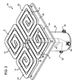
- the bottom induction coil 18 ( Figure 2 ) comprises a plurality of windings 31, 32, 33 and 34, in the embodiment shown having plane development, arranged alongside one another in one and the same plane of lie defined by an insulated supporting plate 35, in turn carried by a stem or hub 36 that is moved within the half-shell 6 by the movement means 30 to vary the distance D in use.
- electrical switching means 40 are prearranged between the windings 31-34 of the bottom induction coil 18 and the respective a.c. electrical-supply means 20 for connecting the windings 31-34 selectively to one another and to the means 20 according to different configurations, which differ from one another as regards the direction of circulation of the electric currents in the respective windings 31-34 set alongside one another, as represented schematically, for example, in Figure 3 .
- the bottom induction coil 18 includes four windings, designated precisely by 31, 32, 33, 34, arranged alongside one another in twos, according to a chequered scheme.
- the windings 31-34 are in particular shaped each as a plane spiral ( Figure 2 ) obtained by bending a number of times on itself a copper tube to form the hollow turns 13 and subdivide the bottom induction coil 18 into respective adjacent sectors, represented schematically in Figure 4 , in which the windings 31-34 are also represented schematically by circular arrows having direction concordant with that of circulation of the electric currents therein, in which sectors respective lines of flux L of the magnetic field generated by the induction coil 18 have a similar pattern.
- the switching means 40 are then such as to be designed to determine selectively between adjacent sectors a pattern of the lines of flux L that is, respectively, tangential (for example Figure 4a ), or normal ( Figure 4c ) to the boundary lines K between one sector and the next, or, again, mixed ( Figure 4b ).
- the cooling means 21 of at least the bottom induction coil 18 are designed to supply in the hollow turns 13 thereof a diathermic oil or else water, through the hub or stem 36, by means of respective pipe unions 50, for example, one in number for each winding 31-34; in particular, each winding 31-34 starts and terminates with a mouth 60 ( Figure 2 ), connected via hydraulic lines 61 inside the hub or stem 36 with the pipe unions 50, which are in turn connected in a known way with the cooling means 21 .
- the device 1 it is possible to implement effectively a method for carrying out control of the temperature of the semiconductor material 2 in a process for directional solidification of said material, in which the latter is melted and is subsequently subjected to controlled solidification and in which the melting step is performed by heating the semiconductor material contained in the crucible 3 by means of graphite susceptors 14, 17, 19, each operatively associated to at least one respective induction coil, 12, 16, and 18, respectively, and arranged so as to surround the crucible 3.
- the method for controlling the temperature of the silicon 2 in the crucible 3 comprises the steps of:
- each winding 31-34 of the bottom induction coil 18 are connected to one another so that each winding 31-34 defines a sector of the induction coil 18 in which respective lines of flux L of the magnetic field have a similar pattern, and so that, in combination, the lines of flux L of adjacent sectors have a pattern respectively always tangential ( Figure 3a ) or normal ( Figure 3c ) to the boundary line K between one sector and the next.
- the distance D between the bottom induction coil 18 and the respective graphite susceptor 19 associated thereto is varied according to the method of the invention, according to the need and, in particular, during the step of directional solidification, which is performed by interrupting the electrical supply of the bottom induction coil 18, keeping, however, in circulation a coolant in the hollow turns 13 thereof, and approaching the induction coil 18 to the susceptor 19 associated thereto until it is brought substantially into contact therewith, using as coolant a diathermic oil or else water, as already mentioned.
- the induction coil 18 is set within a compartment defined by respective thermally insulating elements 100 that surround the susceptors 14, 17, 19, whereas the induction coils 12 and 16 are preferably arranged on the outside of said compartment and, hence, with the insulating elements 100 set between them and the susceptors 14, 17 associated thereto.
- Figure 4 shows in particular the pattern of the temperatures (the areas with higher temperature are the lighter areas, according to the greyscale used in the graph of Figure 4 ) in the susceptor 19 when the configuration of the electric currents in the windings 31-34 is that of Figure 3a.
- Figures 4b and 4c show likewise the appearance of the distribution of the temperatures in the susceptor 19 when the configuration of the electric currents is that of Figure 4b and Figure 4c , respectively.
Landscapes
- Engineering & Computer Science (AREA)
- Chemical & Material Sciences (AREA)
- Organic Chemistry (AREA)
- Crystallography & Structural Chemistry (AREA)
- Materials Engineering (AREA)
- Metallurgy (AREA)
- Physics & Mathematics (AREA)
- Electromagnetism (AREA)
- Mechanical Engineering (AREA)
- General Engineering & Computer Science (AREA)
- Silicon Compounds (AREA)
- Crystals, And After-Treatments Of Crystals (AREA)
- Photovoltaic Devices (AREA)
Claims (13)
- Vorrichtung (1) zum Schmelzen und anschließender richtungsabhängiger Verfestigung eines Halbleitermaterials (2), um typischerweise polykristallines Silizium mit einem "Solar"-Reinheitsgrad zu gewinnen, die aufweist: wenigstens einen Schmelztiegel (3) für das Halbleitermaterial, der vorzugsweise aus Quarz oder keramischem Material besteht, der entfernbar in einem becherförmigen Graphitbehälter (4) untergebracht ist; wenigstens eine obere Induktionsspule (12), die wenigstens unter Einfügung einer Graphitplatte (14) eingerichtet ist, die betriebsfähig damit verbunden ist und einer Mündung (15) des Graphitbehälters zugewandt ist; wenigstens eine seitliche Induktionsspule (16), die um eine Seitenwand (17) des Graphitbehälters herum eingerichtet ist; wenigstens eine untere Induktionsspule (18), die einer Bodenwand (19) des Graphitbehälters zugewandt eingerichtet ist; elektrische Wechselstromversorgungseinrichtungen (20) zum getrennten Versorgen der Induktionsspulen (12, 16, 18) unabhängig voneinander; und Kühleinrichtungen (21) zum Zuführen eines Kühlmittels innerhalb jeweiliger hohler Windungen (13) der Induktionsspulen; wobei die Vorrichtung dadurch gekennzeichnet ist, dass in Kombination:- die wenigstens eine untere Induktionsspule (18) mehrere Wicklungen (31 - 34) aufweist, die längs aneinander in ein und derselben Lagenebene angeordnet sind, die durch eine isolierte Halteplatte (35) definiert wird;- elektrische Schalteinrichtungen (40), die vorab zwischen den Wicklungen (31 - 34) der wenigstens einen unteren Induktionsspule (18) und den jeweiligen elektrischen Wechselstromversorgungseinrichtungen (40) angeordnet sind, um die letzteren und die Wicklungen (31 - 34) gemäß verschiedenen Konfigurationen selektiv miteinander zu verbinden.
- Vorrichtung nach Anspruch 1, dadurch gekennzeichnet, dass die verschiedenen Konfigurationen sich, was die Zirkulationsrichtung elektrischer Ströme in den jeweiligen Wicklungen (31 - 34), die längs aneinander eingerichtet sind, voneinander unterscheiden.
- Vorrichtung nach Anspruch 1 oder Anspruch 2, dadurch gekennzeichnet, dass wenigstens eine untere Induktionsspule (18) vier der Wicklungen (31 - 34) umfasst, die nach einem schachbrettartigen Schema paarweise längs aneinander angeordnet sind.
- Vorrichtung nach einem der vorhergehenden Ansprüche, dadurch gekennzeichnet, dass die längs aneinander angeordneten Wicklungen (31 - 34) eine Ebenenentwicklung haben, die jeweils als eine Ebenenspirale geformt ist.
- Vorrichtung nach einem der vorhergehenden Ansprüche, dadurch gekennzeichnet, dass die Wicklungen (31 - 34) die wenigstens eine untere Induktionsspule (18) in jeweilige benachbarte Sektoren unterteilen, in denen jeweilige Flusslinien (L) des von der Induktionsspule erzeugten Magnetfelds ein ähnliches Muster haben; dass die Schalteinrichtungen (40) derart konstruiert sind, dass sie selektiv zwischen benachbarten Sektoren eines Musters der Flusslinien (L) jeweils tangential oder normal zu der Grenzlinie (K) zwischen einem Sektor und dem nächsten entscheiden.
- Vorrichtung nach einem der vorhergehenden Ansprüche, dadurch gekennzeichnet, dass wenigstens eine untere Induktionsspule (18) vertikal mobil ist, so dass sie fähig ist, ihren Abstand (D) von der Bodenwand (19) des Graphitbehälters (4) zu verändern.
- Vorrichtung nach einem der vorhergehenden Ansprüche, dadurch gekennzeichnet, dass die Kühleinrichtungen (21) wenigstens der unteren Induktionsspule (18) konstruiert sind, um ein diathermisches Öl in ihren hohlen Windungen (13) zuzuführen.
- Vorrichtung nach einem der vorhergehenden Ansprüche, dadurch gekennzeichnet, dass sie ferner ein zu öffnendes fluiddichtes Gehäuse (5) aufweist, das in seinem Inneren den Graphitbehälter (4) und die Induktionsspulen (12, 16, 18) aufweist.
- Verfahren zum Durchführen der Steuerung der Temperatur in einem Verfahren zur richtungsabhängigen Verfestigung eines Halbleitermaterials, wobei das Halbleitermaterial geschmolzen wird und anschließend einer gesteuerten Verfestigung unterzogen wird, wobei der Schmelzschritt durchgeführt wird, indem das in einem Schmelztiegel (3) enthaltene Halbleitermaterial mit Hilfe von Graphitsuszeptoren (14, 17, 19) geheizt wird, von denen jeder betriebsfähig mit wenigstens einer jeweiligen Induktionsspule (12, 16, 18) verbunden ist und angeordnet ist, um den Schmelztiegel zu umgeben, wobei das Verfahren dadurch gekennzeichnet ist, dass es die folgenden Schritte aufweist:- Einrichten eines Suszeptors (19), der betriebsfähig mit wenigstens einer unteren Induktionsspule (18), die mehrere längs aneinander in ein und derselben Lagenebene angeordnete Wicklungen (31 - 34) aufweist, verbunden ist, unter dem Schmelztiegel (3); und- selektives Verbinden der Wicklungen (31 - 34) miteinander und mit jeweiligen elektrischen Wechselstromversorgungseinrichtungen (40) für die Versorgung der unteren Induktionsspule gemäß verschiedenen Konfigurationen, die sich in Bezug auf die Zirkulationsrichtung der elektrischen Ströme in den jeweiligen längs aneinander festgelegten Wicklungen (31 - 34) voneinander unterscheiden.
- Verfahren nach Anspruch 9, dadurch gekennzeichnet, dass die Wicklungen (31 - 34) der wenigstens einen unteren Induktionsspule (18) miteinander verbunden sind, so dass jede Wicklung einen Sektor der Induktionsspule definiert, in dem jeweiligen Flusslinien (L) des Magnetfelds ein ähnliches Muster haben; und so dass die Flusslinien (L) benachbarter Sektoren in Kombination ein Muster haben, das jeweils tangential oder normal zu der Grenzlinie (K) zwischen einem Sektor und dem nächsten ist.
- Verfahren nach Anspruch 9 oder Anspruch 10, dadurch gekennzeichnet, dass der Abstand (D) zwischen der wenigstens einen unteren Induktionsspule (18) und dem jeweiligen zugeordneten Graphitsuszeptor (19) verändert wird.
- Verfahren nach einem der Ansprüche 9 bis 11, dadurch gekennzeichnet, dass der Schritt der gesteuerten Verfestigung durchgeführt wird, indem er die elektrische Versorgung der wenigstens einen unteren Induktionsspule (18) unterbricht, wobei ein Kühlmittel in ihren jeweiligen hohlen Windungen (13) zirkulierend gehalten wird und die Induktionsspule (18) dem ihr zugeordneten Suszeptor (19) genähert wird, bis sie im Wesentlichen in Kontakt damit gebracht wird.
- Verfahren nach Anspruch 12, dadurch gekennzeichnet, dass ein diathermisches Öl als Kühlmittel verwendet wird.
Applications Claiming Priority (2)
| Application Number | Priority Date | Filing Date | Title |
|---|---|---|---|
| ITTO2009A000794A IT1396762B1 (it) | 2009-10-21 | 2009-10-21 | Dispositivo per l'ottenimento di un materiale semiconduttore multicristallino, in particolare silicio, e metodo per il controllo della temperatura nello stesso |
| PCT/IB2010/002686 WO2011048474A1 (en) | 2009-10-21 | 2010-10-20 | Device for obtaining a multicrystalline semiconductor material, in particular silicon, and method for controlling the temperature therein |
Publications (2)
| Publication Number | Publication Date |
|---|---|
| EP2491168A1 EP2491168A1 (de) | 2012-08-29 |
| EP2491168B1 true EP2491168B1 (de) | 2013-08-07 |
Family
ID=41796093
Family Applications (1)
| Application Number | Title | Priority Date | Filing Date |
|---|---|---|---|
| EP10787881.1A Active EP2491168B1 (de) | 2009-10-21 | 2010-10-20 | Verfahren zur gewinnung eines polykristallinen halbleitermaterials, im besonderen silizium, und verfahren zur temperaturregelung dafür |
Country Status (7)
| Country | Link |
|---|---|
| US (1) | US20120304697A1 (de) |
| EP (1) | EP2491168B1 (de) |
| JP (1) | JP5681197B2 (de) |
| KR (1) | KR20120099050A (de) |
| CN (1) | CN102753736B (de) |
| IT (1) | IT1396762B1 (de) |
| WO (1) | WO2011048474A1 (de) |
Families Citing this family (8)
| Publication number | Priority date | Publication date | Assignee | Title |
|---|---|---|---|---|
| CN102865944B (zh) * | 2012-09-03 | 2014-04-02 | 中国科学院金属研究所 | 定向凝固过程温度场分布评定方法 |
| KR101496675B1 (ko) * | 2013-08-20 | 2015-02-27 | 주식회사 엘지실트론 | 사파이어 잉곳 성장 장치 |
| CN103966657B (zh) * | 2014-04-17 | 2017-04-19 | 江苏盎华光伏工程技术研究中心有限公司 | 一种多晶硅和准单晶硅铸锭炉及其使用方法 |
| CN104674342A (zh) * | 2015-03-20 | 2015-06-03 | 重庆大全新能源有限公司 | 一种铸锭炉 |
| CN108770105A (zh) * | 2018-05-31 | 2018-11-06 | 广西电网有限责任公司电力科学研究院 | 互感器加热装置 |
| AT522892A1 (de) * | 2019-08-26 | 2021-03-15 | Lkr Leichtmetallkompetenzzentrum Ranshofen Gmbh | Vorrichtung und Verfahren zur Herstellung eines Gussstückes bevorzugt als Vormaterial |
| KR102271716B1 (ko) * | 2020-09-28 | 2021-07-01 | 한화솔루션 주식회사 | 잉곳 성장 장치 |
| CN118684225A (zh) * | 2024-06-06 | 2024-09-24 | 无锡应达工业有限公司 | 一种底部装卸料真空感应卤素石墨净化处理炉系统 |
Family Cites Families (10)
| Publication number | Priority date | Publication date | Assignee | Title |
|---|---|---|---|---|
| BE857189A (fr) * | 1977-07-27 | 1978-01-27 | Elphiac Sa | Four a induction a creuset |
| FR2751738B1 (fr) * | 1996-07-25 | 1998-08-28 | Commissariat Energie Atomique | Four de fusion par induction directe en creuset froid |
| JP3520957B2 (ja) * | 1997-06-23 | 2004-04-19 | シャープ株式会社 | 多結晶半導体インゴットの製造方法および装置 |
| JP3523986B2 (ja) * | 1997-07-02 | 2004-04-26 | シャープ株式会社 | 多結晶半導体の製造方法および製造装置 |
| JP2006275425A (ja) * | 2005-03-29 | 2006-10-12 | Kyocera Corp | 坩堝および半導体インゴットの製造方法 |
| FR2895749B1 (fr) * | 2006-01-04 | 2008-05-02 | Apollon Solar Soc Par Actions | Dispositif et procede de fabrication d'un bloc de materiau cristallin |
| FR2909990B1 (fr) * | 2006-12-13 | 2009-03-13 | Efd Induction Sa Sa | Procede et installation de fabrication de blocs d'un materiau semiconducteur |
| US20080178793A1 (en) * | 2007-01-31 | 2008-07-31 | Calisolar, Inc. | Method and system for forming a higher purity semiconductor ingot using low purity semiconductor feedstock |
| KR100955221B1 (ko) * | 2007-10-05 | 2010-04-29 | 주식회사 글로실 | 힌지를 이용한 도어 개폐장치가 구비된 태양전지용 다결정실리콘 주괴 제조 장치 |
| IT1396761B1 (it) * | 2009-10-21 | 2012-12-14 | Saet Spa | Metodo e dispositivo per l'ottenimento di un materiale semiconduttore multicristallino, in particolare silicio |
-
2009
- 2009-10-21 IT ITTO2009A000794A patent/IT1396762B1/it active
-
2010
- 2010-10-20 EP EP10787881.1A patent/EP2491168B1/de active Active
- 2010-10-20 KR KR1020127012946A patent/KR20120099050A/ko not_active Abandoned
- 2010-10-20 WO PCT/IB2010/002686 patent/WO2011048474A1/en not_active Ceased
- 2010-10-20 JP JP2012534788A patent/JP5681197B2/ja not_active Expired - Fee Related
- 2010-10-20 US US13/503,283 patent/US20120304697A1/en not_active Abandoned
- 2010-10-20 CN CN201080058771.6A patent/CN102753736B/zh not_active Expired - Fee Related
Also Published As
| Publication number | Publication date |
|---|---|
| CN102753736B (zh) | 2015-07-08 |
| US20120304697A1 (en) | 2012-12-06 |
| EP2491168A1 (de) | 2012-08-29 |
| IT1396762B1 (it) | 2012-12-14 |
| JP2013508252A (ja) | 2013-03-07 |
| ITTO20090794A1 (it) | 2011-04-22 |
| KR20120099050A (ko) | 2012-09-06 |
| CN102753736A (zh) | 2012-10-24 |
| JP5681197B2 (ja) | 2015-03-04 |
| WO2011048474A1 (en) | 2011-04-28 |
Similar Documents
| Publication | Publication Date | Title |
|---|---|---|
| EP2491169B1 (de) | Verfahren und vorrichtung zur gewinnung eines polykristallinen halbleitermaterials, im besonderen silizium | |
| US20120304697A1 (en) | Device for obtaining a multicrystalline semiconductor material, in particular silicon, and method for controlling the temperature therein | |
| US9303331B2 (en) | Heater assembly for crystal growth apparatus | |
| US8242420B2 (en) | Directional solidification of silicon by electric induction susceptor heating in a controlled environment | |
| US8729435B2 (en) | Purification of silicon by electric induction melting and directional partial cooling of the melt | |
| EP2640874B1 (de) | Vorrichtung und verfahren zur gerichteten festigung von silizium | |
| CN103966657B (zh) | 一种多晶硅和准单晶硅铸锭炉及其使用方法 | |
| WO2000056482A1 (en) | Casting of high purity oxygen free copper | |
| JP5959084B2 (ja) | シリコンの制御された方向性凝固 | |
| CA2779659C (en) | Silicon electromagnetic casting apparatus | |
| JP4664967B2 (ja) | シリコン鋳造装置およびシリコン基板の製造方法 | |
| JP5371701B2 (ja) | 多結晶シリコンインゴットの製造装置及び多結晶シリコンインゴットの製造方法 | |
| EP1945003B1 (de) | Gerichtete Erstarrung eines Metalls | |
| KR100712139B1 (ko) | 브릿지만 공정을 이용한 단결정 생성장치 및 생성방법 | |
| WO2012011159A1 (ja) | シリコンインゴットの連続鋳造方法 | |
| AU2013204598A1 (en) | Electromagnetic casting apparatus for silicon | |
| JP2005154226A (ja) | 単結晶の育成方法 | |
| HK1123436A (en) | Directional solidification of a metal | |
| JP2013056812A (ja) | 多結晶シリコンインゴットの製造方法 |
Legal Events
| Date | Code | Title | Description |
|---|---|---|---|
| PUAI | Public reference made under article 153(3) epc to a published international application that has entered the european phase |
Free format text: ORIGINAL CODE: 0009012 |
|
| 17P | Request for examination filed |
Effective date: 20120430 |
|
| AK | Designated contracting states |
Kind code of ref document: A1 Designated state(s): AL AT BE BG CH CY CZ DE DK EE ES FI FR GB GR HR HU IE IS IT LI LT LU LV MC MK MT NL NO PL PT RO RS SE SI SK SM TR |
|
| AX | Request for extension of the european patent |
Extension state: BA ME |
|
| REG | Reference to a national code |
Ref country code: DE Ref legal event code: R079 Ref document number: 602010009276 Country of ref document: DE Free format text: PREVIOUS MAIN CLASS: C30B0011000000 Ipc: H05B0006240000 |
|
| GRAP | Despatch of communication of intention to grant a patent |
Free format text: ORIGINAL CODE: EPIDOSNIGR1 |
|
| RIC1 | Information provided on ipc code assigned before grant |
Ipc: C30B 11/00 20060101ALI20130125BHEP Ipc: C30B 35/00 20060101ALI20130125BHEP Ipc: H05B 6/24 20060101AFI20130125BHEP Ipc: C30B 29/06 20060101ALI20130125BHEP Ipc: B22D 27/04 20060101ALI20130125BHEP Ipc: H05B 6/36 20060101ALI20130125BHEP Ipc: F27B 14/14 20060101ALI20130125BHEP Ipc: H05B 6/44 20060101ALI20130125BHEP |
|
| GRAS | Grant fee paid |
Free format text: ORIGINAL CODE: EPIDOSNIGR3 |
|
| GRAA | (expected) grant |
Free format text: ORIGINAL CODE: 0009210 |
|
| AK | Designated contracting states |
Kind code of ref document: B1 Designated state(s): AL AT BE BG CH CY CZ DE DK EE ES FI FR GB GR HR HU IE IS IT LI LT LU LV MC MK MT NL NO PL PT RO RS SE SI SK SM TR |
|
| AX | Request for extension of the european patent |
Extension state: BA ME |
|
| REG | Reference to a national code |
Ref country code: GB Ref legal event code: FG4D |
|
| REG | Reference to a national code |
Ref country code: CH Ref legal event code: EP Ref country code: AT Ref legal event code: REF Ref document number: 626209 Country of ref document: AT Kind code of ref document: T Effective date: 20130815 |
|
| REG | Reference to a national code |
Ref country code: IE Ref legal event code: FG4D |
|
| REG | Reference to a national code |
Ref country code: DE Ref legal event code: R096 Ref document number: 602010009276 Country of ref document: DE Effective date: 20131002 |
|
| REG | Reference to a national code |
Ref country code: AT Ref legal event code: MK05 Ref document number: 626209 Country of ref document: AT Kind code of ref document: T Effective date: 20130807 |
|
| REG | Reference to a national code |
Ref country code: NL Ref legal event code: VDEP Effective date: 20130807 |
|
| REG | Reference to a national code |
Ref country code: NO Ref legal event code: T2 Effective date: 20130807 |
|
| REG | Reference to a national code |
Ref country code: LT Ref legal event code: MG4D |
|
| PG25 | Lapsed in a contracting state [announced via postgrant information from national office to epo] |
Ref country code: IS Free format text: LAPSE BECAUSE OF FAILURE TO SUBMIT A TRANSLATION OF THE DESCRIPTION OR TO PAY THE FEE WITHIN THE PRESCRIBED TIME-LIMIT Effective date: 20131207 Ref country code: HR Free format text: LAPSE BECAUSE OF FAILURE TO SUBMIT A TRANSLATION OF THE DESCRIPTION OR TO PAY THE FEE WITHIN THE PRESCRIBED TIME-LIMIT Effective date: 20130807 Ref country code: SE Free format text: LAPSE BECAUSE OF FAILURE TO SUBMIT A TRANSLATION OF THE DESCRIPTION OR TO PAY THE FEE WITHIN THE PRESCRIBED TIME-LIMIT Effective date: 20130807 Ref country code: CY Free format text: LAPSE BECAUSE OF FAILURE TO SUBMIT A TRANSLATION OF THE DESCRIPTION OR TO PAY THE FEE WITHIN THE PRESCRIBED TIME-LIMIT Effective date: 20130911 Ref country code: AT Free format text: LAPSE BECAUSE OF FAILURE TO SUBMIT A TRANSLATION OF THE DESCRIPTION OR TO PAY THE FEE WITHIN THE PRESCRIBED TIME-LIMIT Effective date: 20130807 Ref country code: PT Free format text: LAPSE BECAUSE OF FAILURE TO SUBMIT A TRANSLATION OF THE DESCRIPTION OR TO PAY THE FEE WITHIN THE PRESCRIBED TIME-LIMIT Effective date: 20131209 Ref country code: LT Free format text: LAPSE BECAUSE OF FAILURE TO SUBMIT A TRANSLATION OF THE DESCRIPTION OR TO PAY THE FEE WITHIN THE PRESCRIBED TIME-LIMIT Effective date: 20130807 |
|
| PG25 | Lapsed in a contracting state [announced via postgrant information from national office to epo] |
Ref country code: LV Free format text: LAPSE BECAUSE OF FAILURE TO SUBMIT A TRANSLATION OF THE DESCRIPTION OR TO PAY THE FEE WITHIN THE PRESCRIBED TIME-LIMIT Effective date: 20130807 Ref country code: PL Free format text: LAPSE BECAUSE OF FAILURE TO SUBMIT A TRANSLATION OF THE DESCRIPTION OR TO PAY THE FEE WITHIN THE PRESCRIBED TIME-LIMIT Effective date: 20130807 Ref country code: NL Free format text: LAPSE BECAUSE OF FAILURE TO SUBMIT A TRANSLATION OF THE DESCRIPTION OR TO PAY THE FEE WITHIN THE PRESCRIBED TIME-LIMIT Effective date: 20130807 Ref country code: BE Free format text: LAPSE BECAUSE OF FAILURE TO SUBMIT A TRANSLATION OF THE DESCRIPTION OR TO PAY THE FEE WITHIN THE PRESCRIBED TIME-LIMIT Effective date: 20130807 Ref country code: SI Free format text: LAPSE BECAUSE OF FAILURE TO SUBMIT A TRANSLATION OF THE DESCRIPTION OR TO PAY THE FEE WITHIN THE PRESCRIBED TIME-LIMIT Effective date: 20130807 Ref country code: FI Free format text: LAPSE BECAUSE OF FAILURE TO SUBMIT A TRANSLATION OF THE DESCRIPTION OR TO PAY THE FEE WITHIN THE PRESCRIBED TIME-LIMIT Effective date: 20130807 Ref country code: GR Free format text: LAPSE BECAUSE OF FAILURE TO SUBMIT A TRANSLATION OF THE DESCRIPTION OR TO PAY THE FEE WITHIN THE PRESCRIBED TIME-LIMIT Effective date: 20131108 |
|
| PG25 | Lapsed in a contracting state [announced via postgrant information from national office to epo] |
Ref country code: CY Free format text: LAPSE BECAUSE OF FAILURE TO SUBMIT A TRANSLATION OF THE DESCRIPTION OR TO PAY THE FEE WITHIN THE PRESCRIBED TIME-LIMIT Effective date: 20130807 |
|
| PG25 | Lapsed in a contracting state [announced via postgrant information from national office to epo] |
Ref country code: DK Free format text: LAPSE BECAUSE OF FAILURE TO SUBMIT A TRANSLATION OF THE DESCRIPTION OR TO PAY THE FEE WITHIN THE PRESCRIBED TIME-LIMIT Effective date: 20130807 Ref country code: CZ Free format text: LAPSE BECAUSE OF FAILURE TO SUBMIT A TRANSLATION OF THE DESCRIPTION OR TO PAY THE FEE WITHIN THE PRESCRIBED TIME-LIMIT Effective date: 20130807 Ref country code: RO Free format text: LAPSE BECAUSE OF FAILURE TO SUBMIT A TRANSLATION OF THE DESCRIPTION OR TO PAY THE FEE WITHIN THE PRESCRIBED TIME-LIMIT Effective date: 20130807 Ref country code: SK Free format text: LAPSE BECAUSE OF FAILURE TO SUBMIT A TRANSLATION OF THE DESCRIPTION OR TO PAY THE FEE WITHIN THE PRESCRIBED TIME-LIMIT Effective date: 20130807 Ref country code: EE Free format text: LAPSE BECAUSE OF FAILURE TO SUBMIT A TRANSLATION OF THE DESCRIPTION OR TO PAY THE FEE WITHIN THE PRESCRIBED TIME-LIMIT Effective date: 20130807 |
|
| PG25 | Lapsed in a contracting state [announced via postgrant information from national office to epo] |
Ref country code: IT Free format text: LAPSE BECAUSE OF FAILURE TO SUBMIT A TRANSLATION OF THE DESCRIPTION OR TO PAY THE FEE WITHIN THE PRESCRIBED TIME-LIMIT Effective date: 20130807 Ref country code: ES Free format text: LAPSE BECAUSE OF FAILURE TO SUBMIT A TRANSLATION OF THE DESCRIPTION OR TO PAY THE FEE WITHIN THE PRESCRIBED TIME-LIMIT Effective date: 20130807 Ref country code: MC Free format text: LAPSE BECAUSE OF FAILURE TO SUBMIT A TRANSLATION OF THE DESCRIPTION OR TO PAY THE FEE WITHIN THE PRESCRIBED TIME-LIMIT Effective date: 20130807 |
|
| PLBE | No opposition filed within time limit |
Free format text: ORIGINAL CODE: 0009261 |
|
| STAA | Information on the status of an ep patent application or granted ep patent |
Free format text: STATUS: NO OPPOSITION FILED WITHIN TIME LIMIT |
|
| 26N | No opposition filed |
Effective date: 20140508 |
|
| REG | Reference to a national code |
Ref country code: IE Ref legal event code: MM4A |
|
| REG | Reference to a national code |
Ref country code: DE Ref legal event code: R097 Ref document number: 602010009276 Country of ref document: DE Effective date: 20140508 |
|
| PG25 | Lapsed in a contracting state [announced via postgrant information from national office to epo] |
Ref country code: IE Free format text: LAPSE BECAUSE OF NON-PAYMENT OF DUE FEES Effective date: 20131020 |
|
| PGFP | Annual fee paid to national office [announced via postgrant information from national office to epo] |
Ref country code: NO Payment date: 20141009 Year of fee payment: 5 Ref country code: DE Payment date: 20141014 Year of fee payment: 5 Ref country code: FR Payment date: 20141008 Year of fee payment: 5 |
|
| PG25 | Lapsed in a contracting state [announced via postgrant information from national office to epo] |
Ref country code: SM Free format text: LAPSE BECAUSE OF FAILURE TO SUBMIT A TRANSLATION OF THE DESCRIPTION OR TO PAY THE FEE WITHIN THE PRESCRIBED TIME-LIMIT Effective date: 20130807 |
|
| REG | Reference to a national code |
Ref country code: CH Ref legal event code: PL |
|
| GBPC | Gb: european patent ceased through non-payment of renewal fee |
Effective date: 20141020 |
|
| PG25 | Lapsed in a contracting state [announced via postgrant information from national office to epo] |
Ref country code: GB Free format text: LAPSE BECAUSE OF NON-PAYMENT OF DUE FEES Effective date: 20141020 Ref country code: LI Free format text: LAPSE BECAUSE OF NON-PAYMENT OF DUE FEES Effective date: 20141031 Ref country code: CH Free format text: LAPSE BECAUSE OF NON-PAYMENT OF DUE FEES Effective date: 20141031 Ref country code: LU Free format text: LAPSE BECAUSE OF NON-PAYMENT OF DUE FEES Effective date: 20131020 Ref country code: BG Free format text: LAPSE BECAUSE OF FAILURE TO SUBMIT A TRANSLATION OF THE DESCRIPTION OR TO PAY THE FEE WITHIN THE PRESCRIBED TIME-LIMIT Effective date: 20130807 Ref country code: MK Free format text: LAPSE BECAUSE OF FAILURE TO SUBMIT A TRANSLATION OF THE DESCRIPTION OR TO PAY THE FEE WITHIN THE PRESCRIBED TIME-LIMIT Effective date: 20130807 Ref country code: RS Free format text: LAPSE BECAUSE OF FAILURE TO SUBMIT A TRANSLATION OF THE DESCRIPTION OR TO PAY THE FEE WITHIN THE PRESCRIBED TIME-LIMIT Effective date: 20131107 Ref country code: HU Free format text: LAPSE BECAUSE OF FAILURE TO SUBMIT A TRANSLATION OF THE DESCRIPTION OR TO PAY THE FEE WITHIN THE PRESCRIBED TIME-LIMIT; INVALID AB INITIO Effective date: 20101020 |
|
| PG25 | Lapsed in a contracting state [announced via postgrant information from national office to epo] |
Ref country code: MT Free format text: LAPSE BECAUSE OF FAILURE TO SUBMIT A TRANSLATION OF THE DESCRIPTION OR TO PAY THE FEE WITHIN THE PRESCRIBED TIME-LIMIT Effective date: 20130807 |
|
| REG | Reference to a national code |
Ref country code: DE Ref legal event code: R119 Ref document number: 602010009276 Country of ref document: DE |
|
| REG | Reference to a national code |
Ref country code: NO Ref legal event code: MMEP |
|
| PG25 | Lapsed in a contracting state [announced via postgrant information from national office to epo] |
Ref country code: NO Free format text: LAPSE BECAUSE OF NON-PAYMENT OF DUE FEES Effective date: 20151031 Ref country code: TR Free format text: LAPSE BECAUSE OF FAILURE TO SUBMIT A TRANSLATION OF THE DESCRIPTION OR TO PAY THE FEE WITHIN THE PRESCRIBED TIME-LIMIT Effective date: 20130807 Ref country code: DE Free format text: LAPSE BECAUSE OF NON-PAYMENT OF DUE FEES Effective date: 20160503 |
|
| REG | Reference to a national code |
Ref country code: FR Ref legal event code: ST Effective date: 20160630 |
|
| PG25 | Lapsed in a contracting state [announced via postgrant information from national office to epo] |
Ref country code: FR Free format text: LAPSE BECAUSE OF NON-PAYMENT OF DUE FEES Effective date: 20151102 |
|
| PG25 | Lapsed in a contracting state [announced via postgrant information from national office to epo] |
Ref country code: AL Free format text: LAPSE BECAUSE OF FAILURE TO SUBMIT A TRANSLATION OF THE DESCRIPTION OR TO PAY THE FEE WITHIN THE PRESCRIBED TIME-LIMIT Effective date: 20130807 |