EP2485281A1 - Light-emitting element - Google Patents
Light-emitting element Download PDFInfo
- Publication number
- EP2485281A1 EP2485281A1 EP10807510A EP10807510A EP2485281A1 EP 2485281 A1 EP2485281 A1 EP 2485281A1 EP 10807510 A EP10807510 A EP 10807510A EP 10807510 A EP10807510 A EP 10807510A EP 2485281 A1 EP2485281 A1 EP 2485281A1
- Authority
- EP
- European Patent Office
- Prior art keywords
- layer
- light emitting
- light
- gallium nitride
- emitting device
- Prior art date
- Legal status (The legal status is an assumption and is not a legal conclusion. Google has not performed a legal analysis and makes no representation as to the accuracy of the status listed.)
- Withdrawn
Links
- 229910002601 GaN Inorganic materials 0.000 claims abstract description 106
- JMASRVWKEDWRBT-UHFFFAOYSA-N Gallium nitride Chemical compound [Ga]#N JMASRVWKEDWRBT-UHFFFAOYSA-N 0.000 claims abstract description 38
- 239000004065 semiconductor Substances 0.000 claims abstract description 33
- 239000000758 substrate Substances 0.000 claims abstract description 23
- 230000010287 polarization Effects 0.000 claims abstract description 20
- 239000000463 material Substances 0.000 claims abstract description 13
- OAICVXFJPJFONN-UHFFFAOYSA-N Phosphorus Chemical compound [P] OAICVXFJPJFONN-UHFFFAOYSA-N 0.000 claims description 30
- 229910052738 indium Inorganic materials 0.000 claims description 16
- APFVFJFRJDLVQX-UHFFFAOYSA-N indium atom Chemical compound [In] APFVFJFRJDLVQX-UHFFFAOYSA-N 0.000 claims description 16
- GYHNNYVSQQEPJS-UHFFFAOYSA-N Gallium Chemical compound [Ga] GYHNNYVSQQEPJS-UHFFFAOYSA-N 0.000 claims description 12
- 229910052733 gallium Inorganic materials 0.000 claims description 12
- 229910052782 aluminium Inorganic materials 0.000 claims description 9
- XAGFODPZIPBFFR-UHFFFAOYSA-N aluminium Chemical compound [Al] XAGFODPZIPBFFR-UHFFFAOYSA-N 0.000 claims description 9
- 239000000460 chlorine Substances 0.000 claims description 7
- WKBOTKDWSSQWDR-UHFFFAOYSA-N Bromine atom Chemical compound [Br] WKBOTKDWSSQWDR-UHFFFAOYSA-N 0.000 claims description 6
- ZAMOUSCENKQFHK-UHFFFAOYSA-N Chlorine atom Chemical compound [Cl] ZAMOUSCENKQFHK-UHFFFAOYSA-N 0.000 claims description 6
- GDTBXPJZTBHREO-UHFFFAOYSA-N bromine Substances BrBr GDTBXPJZTBHREO-UHFFFAOYSA-N 0.000 claims description 6
- 229910052794 bromium Inorganic materials 0.000 claims description 6
- 229910052801 chlorine Inorganic materials 0.000 claims description 6
- 239000012535 impurity Substances 0.000 claims description 6
- ZCYVEMRRCGMTRW-UHFFFAOYSA-N 7553-56-2 Chemical compound [I] ZCYVEMRRCGMTRW-UHFFFAOYSA-N 0.000 claims description 5
- 229910052740 iodine Inorganic materials 0.000 claims description 5
- 239000011630 iodine Substances 0.000 claims description 5
- 239000002131 composite material Substances 0.000 abstract description 14
- 150000004767 nitrides Chemical class 0.000 description 15
- 239000000203 mixture Substances 0.000 description 8
- 230000004888 barrier function Effects 0.000 description 7
- 229910002704 AlGaN Inorganic materials 0.000 description 5
- 238000000407 epitaxy Methods 0.000 description 5
- 238000007740 vapor deposition Methods 0.000 description 5
- 238000010521 absorption reaction Methods 0.000 description 4
- 239000010931 gold Substances 0.000 description 4
- 230000003746 surface roughness Effects 0.000 description 4
- 239000010936 titanium Substances 0.000 description 4
- PXHVJJICTQNCMI-UHFFFAOYSA-N Nickel Chemical compound [Ni] PXHVJJICTQNCMI-UHFFFAOYSA-N 0.000 description 3
- 239000003086 colorant Substances 0.000 description 3
- 239000013078 crystal Substances 0.000 description 3
- 238000003475 lamination Methods 0.000 description 3
- 238000004519 manufacturing process Methods 0.000 description 3
- RTAQQCXQSZGOHL-UHFFFAOYSA-N Titanium Chemical compound [Ti] RTAQQCXQSZGOHL-UHFFFAOYSA-N 0.000 description 2
- 238000005520 cutting process Methods 0.000 description 2
- 229910052737 gold Inorganic materials 0.000 description 2
- 238000002347 injection Methods 0.000 description 2
- 239000007924 injection Substances 0.000 description 2
- 238000000034 method Methods 0.000 description 2
- SBIBMFFZSBJNJF-UHFFFAOYSA-N selenium;zinc Chemical compound [Se]=[Zn] SBIBMFFZSBJNJF-UHFFFAOYSA-N 0.000 description 2
- 229910052719 titanium Inorganic materials 0.000 description 2
- 230000000694 effects Effects 0.000 description 1
- 230000001747 exhibiting effect Effects 0.000 description 1
- PNDPGZBMCMUPRI-UHFFFAOYSA-N iodine Chemical compound II PNDPGZBMCMUPRI-UHFFFAOYSA-N 0.000 description 1
- 229910052751 metal Inorganic materials 0.000 description 1
- 239000002184 metal Substances 0.000 description 1
- 229910052759 nickel Inorganic materials 0.000 description 1
- 230000003287 optical effect Effects 0.000 description 1
- 238000002310 reflectometry Methods 0.000 description 1
- 229910052594 sapphire Inorganic materials 0.000 description 1
- 239000010980 sapphire Substances 0.000 description 1
- 229910052709 silver Inorganic materials 0.000 description 1
- 239000004332 silver Substances 0.000 description 1
- 239000000243 solution Substances 0.000 description 1
Images


Classifications
-
- H—ELECTRICITY
- H10—SEMICONDUCTOR DEVICES; ELECTRIC SOLID-STATE DEVICES NOT OTHERWISE PROVIDED FOR
- H10H—INORGANIC LIGHT-EMITTING SEMICONDUCTOR DEVICES HAVING POTENTIAL BARRIERS
- H10H20/00—Individual inorganic light-emitting semiconductor devices having potential barriers, e.g. light-emitting diodes [LED]
- H10H20/80—Constructional details
- H10H20/81—Bodies
- H10H20/817—Bodies characterised by the crystal structures or orientations, e.g. polycrystalline, amorphous or porous
-
- H—ELECTRICITY
- H10—SEMICONDUCTOR DEVICES; ELECTRIC SOLID-STATE DEVICES NOT OTHERWISE PROVIDED FOR
- H10H—INORGANIC LIGHT-EMITTING SEMICONDUCTOR DEVICES HAVING POTENTIAL BARRIERS
- H10H20/00—Individual inorganic light-emitting semiconductor devices having potential barriers, e.g. light-emitting diodes [LED]
- H10H20/80—Constructional details
- H10H20/81—Bodies
- H10H20/813—Bodies having a plurality of light-emitting regions, e.g. multi-junction LEDs or light-emitting devices having photoluminescent regions within the bodies
-
- H—ELECTRICITY
- H10—SEMICONDUCTOR DEVICES; ELECTRIC SOLID-STATE DEVICES NOT OTHERWISE PROVIDED FOR
- H10H—INORGANIC LIGHT-EMITTING SEMICONDUCTOR DEVICES HAVING POTENTIAL BARRIERS
- H10H20/00—Individual inorganic light-emitting semiconductor devices having potential barriers, e.g. light-emitting diodes [LED]
- H10H20/80—Constructional details
- H10H20/81—Bodies
- H10H20/822—Materials of the light-emitting regions
- H10H20/824—Materials of the light-emitting regions comprising only Group III-V materials, e.g. GaP
- H10H20/825—Materials of the light-emitting regions comprising only Group III-V materials, e.g. GaP containing nitrogen, e.g. GaN
Definitions
- the present invention relates to a light emitting device.
- Patent Literature 1 discloses a nitride semiconductor light emitting device comprising a GaN semiconductor layer formed on a GaN substrate, the GaN semiconductor layer including a first and second quantum well layers that emit light having different wavelengths. A color mixture of colors of light components emitted from the first and second active layers is observed.
- Patent Literature 2 discloses a light emitting device comprising a blue light emitting diode chip and a yellow light emitting diode chip that are mounted on a supporting substrate, thereby producing white light obtained by mixing light components emitted from the two light emitting diodes.
- Patent Literature 3 discloses a light emitting device comprising a group-III nitride semiconductor substrate and an active layer, the group-III nitride semiconductor substrate emitting longer-wavelength light induced by absorption of ultraviolet light, and the active layer being disposed on the group-III nitride semiconductor substrate and emitting light including the ultraviolet light component.
- Patent Literature 4 discloses a white light emitting device comprising an InGaN-LED that emits blue light and a ZnSSe fluorescent plate that emits yellow light induced by absorption of the blue light.
- Patent Literature 5 discloses a wavelength converter that emits light having a different wavelength from that of incident light by means of a phosphor contained in a composite substrate.
- Patent Literature 6 and Patent Literature 7 disclose art concerning composite substrates.
- Non-patent Literature 1 discloses polarization of light emitted from an InGaN well layer.
- a light emitting device comprises: a substrate; and a hexagonal gallium nitride-based semiconductor layer having a light emitting layer which contains indium, the substrate including a base and a gallium nitride layer which has a thickness less than a thickness of the base, the hexagonal gallium nitride-based semiconductor layer being disposed on a principal surface of the gallium nitride layer, an angle between a c-axis of the gallium nitride layer and a normal line to the principal surface of the gallium nitride layer being in a range of not less than 50 degree and not more than 130 degree, the light emitting layer emitting light with an absolute value of the degree of polarization of not less than 0.2, the base containing a fluorescent material that emits a fluorescent light component which is induced by irradiation of a light component emitted from the light emitting layer.
- the light emitting device can emit light produced by superposition of a light component emitted from the light emitting layer and a light component induced by a light component incident on the base from the light emitting layer. Because an angle between the c-axis of the gallium nitride layer and the normal line to the principal surface of the gallium nitride layer is in a range of not less than 50 degree and not more than 130 degree, indium content in the light emitting layer is relatively high, and thus, it allows for emission of high-intensity light.
- the piezoelectric field is relatively weak, and thus, it allows for a relatively smaller variation width in wavelength of light from the light emitting layer which is induced by a variation in drive current.
- the absolute value of the degree of polarization of not less than 0.2 indicates a relatively high degree of polarization.
- the base comprises: a phosphor layer containing the fluorescent material; and a support layer being disposed on a principal surface of the phosphor layer, the gallium nitride layer being disposed on a principal surface of the support layer. This enables a material of the support layer to be selected so as to give satisfactory lamination with the gallium nitride layer.
- the light emitting device further comprising a reflective layer which is disposed on the back surface of the phosphor layer, the reflective layer reflecting light which is emitted from the phosphor layer. Therefore, it allows for an improvement in utilization efficiency of light incident on the phosphor layer.
- the gallium nitride layer has a thickness in a range of not less than 100 nm and not more than 1200 nm. Therefore, it allows for compatibility of high-quality and low cost of the substrate.
- the light emitting layer emits light having a peak wavelength in a range of not less than 430 nm and not more than 490 nm.
- the fluorescent material contains a component that emits light having a peak wavelength in a range of not less than 540 nm and not more than 600 nm. Accordingly, white light can be obtained by superposition of the blue light from the light emitting layer and the yellow light produced by the fluorescence material of the base.
- the fluorescent material contains polycrystalline ZnS x Se 1-x (0 ⁇ x ⁇ 1) doped with at least one impurity element selected from the group consisting of aluminum, indium, gallium, chlorine, bromine, and iodine.
- Polycrystalline ZnS x Se 1-x can absorb blue light to emit yellow light.
- one aspect of the present invention provides a light emitting device that emits stable light having a plurality of wavelengths.
- the light emitting device 1 comprises a composite substrate 3, a gallium nitride-based semiconductor layer 5, a p-electrode 13, a pad electrode 15, and an n-electrode 17.
- the composite substrate 3 includes a base 19 and a GaN layer 21.
- the base 19 contains a fluorescent material that emits a fluorescent light component induced by irradiation of a light component emitted from a light emitting layer 9 as described below.
- the fluorescent material contains a component that emits yellow light having a peak wavelength in a range of not less than 540 nm and not more than 600 nm by absorbing blue light having a peak wavelength in a range of not less than 430 nm and not more than 490 nm.
- the GaN layer 21 is disposed on the base 19.
- the GaN layer 21 is in contact with the base 19.
- the GaN layer 21 has a thickness less than that of the base 19 (hereinafter, "thickness" refers to a width in a direction of a normal line N1 to a principal surface S1 of the GaN layer 21).
- the gallium nitride-based semiconductor layer 5 includes an n-type nitride semiconductor layer 7, a light emitting layer 9, and a p-type nitride semiconductor layer 11.
- the n-type nitride semiconductor layer 7, the light emitting layer 9, and the p-type nitride semiconductor layer 11 comprise a hexagonal gallium nitride-based semiconductor.
- the gallium nitride-based semiconductor layer 5 is disposed on the principal surface S1 of the GaN layer 21.
- the gallium nitride-based semiconductor layer 5 is in contact with the GaN layer 21.
- the gallium nitride-based semiconductor layer 5 is deposited by epitaxially growing on the principal surface S1 of the GaN layer 21.
- the n-type nitride semiconductor layer 7 includes a GaN layer 23 and a buffer layer 25.
- the GaN layer 23 comprises a first region 23a and a second region 23b.
- the first region 23a and the second region 23b are disposed in parallel on the principal surface S1 of the GaN layer 21. Both of the first region 23a and the second region 23b are in contact with the GaN layer 21.
- the buffer layer 25 is disposed on the first region 23a.
- the buffer layer 25 is in contact with the first region 23a.
- the first region 23a, the buffer layer 25, the light emitting layer 9, and the p-type nitride semiconductor layer 11 are deposited in sequence on the principal surface S1 of the GaN layer 21.
- the n-electrode 17 is disposed on the first region 23a and is in ohmic contact with the second region 23b.
- the first region 23a has a thickness greater than that of the second region 23b.
- the light emitting layer 9 includes barrier layers 27 and well layers 29 which are alternatively deposited to form a multiple quantum well structure.
- the light emitting layer 9 is disposed on the buffer layer 25.
- the light emitting layer 9 is in contact with the buffer layer 25.
- the barrier layers 27 and the well layers 29 are alternatively deposited in a direction orthogonal to the normal line N1.
- the light emitting layer 9 emits blue light having a peak wavelength in a range of not less than 430 nm and not more than 490 nm.
- the p-type nitride semiconductor layer 11 includes an electron-blocking layer 31 and a contact layer 33.
- the electron-blocking layer 31 is disposed on the light emitting layer 9.
- the electron-blocking layer 31 is in contact with the light emitting layer 9.
- the contact layer 33 is disposed on the electron-blocking layer 31.
- the contact layer 33 is in contact with the electron-blocking layer 31.
- the p-electrode 13 is disposed on the contact layer 33, and is in ohmic contact with the contact layer 33.
- the pad electrode 15 is disposed on the p-electrode 13 and the contact layer 33.
- the pad electrode 15 is in contact with the contact layer 33 through an apertura of the p-electrode 13. It allows for excellent adhesiveness.
- the base 19 comprises generally polycrystalline ZnSe doped with at least one impurity element selected from the group consisting of aluminum, indium, gallium, chlorine, bromine, and iodine, and preferably polycrystalline ZnS x Se 1-x (0 ⁇ x ⁇ 1) doped with at least one impurity element selected from the group consisting of aluminum, indium, gallium, chlorine, bromine, and iodine.
- the GaN layer 21 comprises n-type-doped GaN.
- the GaN layer 21 generally has a thickness of about 200 nm, and preferably in a range of not less than 100 nm and not more than 1200 nm.
- the GaN layer 21 has a dislocation density of not more than 1 ⁇ 10 7 cm -2 .
- the angle ⁇ between the normal line N1 to the GaN layer 21 and the c-axis of the GaN layer 21 indicates that the principal surface S1 of the GaN layer 21 is identical to the m-plane of GaN crystal.
- the angle ⁇ is preferably in a range of not less than 50 degree and not more than 130 degree.
- the GaN layer 23 comprises n-type-doped GaN, and the first region 23a has a thickness of about 2 ⁇ m.
- the buffer layer 25 comprises n-type-doped InGaN, and has a thickness of about 100 nm.
- the composition ratios of indium and gallium in the buffer layer 25 are 0.02 and 0.98, respectively.
- the barrier layer 27 comprises GaN, and has a thickness of about 15 nm.
- the well layer 29 comprises InGaN, and has a thickness of about 3 nm.
- the composition ratios of indium and gallium in the well layer 29 are 0.17 and 0.83, respectively. Because the angle ⁇ is in a range of not less than 50 degree and not more than 130 degree, the composition ratio of indium in the well layer 29 is relatively high, and thus, the light emitting layer 9 becomes capable of emitting high-intensity blue light.
- the piezoelectric field is relatively weak in the light emitting layer 9, and thus, it allows for a relatively smaller variation width in wavelength of light from the light emitting layer 9 which is induced by a variation in drive current.
- the light emitting layer 9 emits blue light with an absolute value of the degree of polarization of not less than 0.2.
- the degree of polarization is defined by (I1-I2) / (I1+I2), where I1 represents a polarized light component in a direction perpendicular to a direction of the projected c-axis of the hexagonal group-III nitride semiconductor onto a principal surface, and I2 represents a polarized light component in the direction of the projected c-axis of the hexagonal group-III nitride semiconductor onto the principal surface.
- the polarized light component I1 is larger than the polarized light component I2.
- the electron-blocking layer 31 comprises p-type-doped AlGaN, and has a thickness of about 20 nm.
- the composition ratios of aluminum and gallium in the electron-blocking layer 31 are 0.18 and 0.82, respectively.
- the contact layer 33 comprises p-type-doped GaN, and has a thickness of about 50 nm.
- the p-electrode 13 comprises nickel/gold (Ni/Au), the pad electrode 15 titanium/gold (Ti/Au), and the n-electrode 17 titanium/aluminum (Ti/Al).
- a GaN layer 21 is processed so as to have the back surface (the surface opposite to the principal surface S1) with an average surface roughness Ra of not more than 1 nm.
- a base 19 is compressively bonded to the back surface of the GaN layer 21 under heat to laminate the base 19 and the GaN layer 21, and thus, a composite substrate 3 is provided.
- the back surface of the GaN layer 21 having an average surface roughness Ra of not more than 1 nm results in sufficiently strong lamination of the base 19 and the GaN layer 21.
- a gallium nitride-based semiconductor layer 5 is formed on the principal surface S1 of the GaN layer 21.
- An n-type-doped GaN layer (corresponding to a GaN layer 23) is deposited by epitaxy on the principal surface S1 of the GaN layer 21 at a temperature of 840°C into a thickness of about 2 ⁇ m.
- An n-type-doped InGaN layer (corresponding to a buffer layer 25) is deposited by epitaxy on a surface of the GaN layer with a thickness of about 2 ⁇ m at a temperature of 840°C into a thickness of about 100 nm.
- the composition ratios of indium and gallium are 0.02 and 0.98, respectively.
- a light emitting layer (corresponding to a light emitting layer 9) having a multiple quantum well structure including GaN barrier layers (corresponding to barrier layers 27) and InGaN well layers (corresponding to well layers 29) is deposited by epitaxy on a surface of the InGaN layer with a thickness of about 100 nm.
- the composition ratios of indium and gallium are 0.17 and 0.83, respectively.
- Each of the barrier layers is deposited at a temperature of 840°C into a thickness of about 15 nm
- each of the well layers is deposited at a temperature of 780°C into a thickness of about 3 nm.
- a p-type-doped AlGaN layer (corresponding to an electron-blocking layer 31) is deposited on the light emitting layer at a temperature of 840°C into a thickness of about 20 nm.
- the composition ratios of aluminum and gallium are 0.18 and 0.82, respectively.
- a p-type-doped GaN layer (corresponding to a contact layer 33) is deposited on the AlGaN layer at a temperature of 840°C into a thickness of about 50 nm.
- the p-type GaN layer with a thickness of about 50 nm, the p-type AlGaN layer with a thickness of about 20 nm, the light emitting layer, the n-type InGaN layer with a thickness of about 100 nm, and the n-type GaN layer with a thickness of about 2 ⁇ m are dry-etched to form the contact layer 33, the electron-blocking layer 31, the light emitting layer 9, the buffer layer 25, and the GaN layer 23 (a first region 23a and a second region 23b).
- the gallium nitride-based semiconductor layer 5 is deposited by epitaxy on the principal surface S1 of the GaN layer 21.
- a p-electrode 13 is deposited on a surface of the contact layer 33 by vacuum vapor deposition. And then, a pad electrode 15 is deposited on a surface of the contact layer 33 and a surface of the p-electrode 13 by vacuum vapor deposition, and an n-electrode 17 is deposited on a surface of the second region 23b by vacuum vapor deposition.
- the light emitting device 1 fabricated according to the method is operated by current injection.
- the light emitting layer 9 emits blue light having a peak wavelength of 470 nm, while the base 19, excited by absorption of the blue light from the light emitting layer 9, emits yellow light. Accordingly, white light obtained by superposition of the blue light and the yellow light is observed.
- the degree of polarization of the blue light emitted from the light emitting layer 9 is 0.84.
- the light emitting device 1 can emit white light produced by superposition of blue light directly emitted from the light emitting layer 9 and yellow light induced by blue light incident on the base 19 from the light emitting layer 9. Because of the angle ⁇ is in a range of not less than 50 degree and not more than 130 degree, indium content in the light emitting layer 9 is relatively high, and thus, it allows for emission of high-intensity light. Because the angle ⁇ is in a range of not less than 50 degree and not more than 130 degree, the piezoelectric field is relatively weak, and thus, it allows for a relatively smaller variation width in wavelength of light from the light emitting layer 9 which is induced by a variation in drive current. The absolute value of the degree of polarization of not less than 0.2 indicates a relatively high degree of polarization.
- the light emitting device 1a includes a composite substrate 3a in place of the composite substrate 3 of the light emitting device 1 in Fig. 1 .
- the light emitting device 1a includes a reflective layer 35a.
- the light emitting device 1a has the same configuration as the light emitting device 1, except for the composite substrate 3a and the reflective layer 35a.
- the composite substrate 3a has a base 19a and a GaN layer 21a.
- the base 19a includes a phosphor layer 37a and a support layer 39a.
- the reflective layer 35a, the phosphor layer 37a, the support layer 39a, and the GaN layer 21a are deposited in sequence.
- the reflective layer 35a is disposed on the back surface S2 of the phosphor layer 37a.
- the reflective layer 35a is in contact with the phosphor layer 37a.
- the support layer 39a is disposed on a principal surface S3 of the phosphor layer 37a.
- the support layer 39a is in contact with the phosphor layer 37a.
- the GaN layer 21a is disposed on a principal surface S4 of the support layer 39a.
- the GaN layer 21a is in contact with the support layer 39a.
- the reflective layer 35a reflects light emitted from the phosphor layer 37a, and comprises a metal that has high reflectivity (for example, silver).
- the phosphor layer 37a having a thickness sufficient to absorb substantially all blue light incident thereon from a light emitting layer 9, places no limitation on flatness of the interface between the phosphor layer 37a and the reflective layer 35a.
- the phosphor layer 37a having a thickness sufficiently less than such a thickness, preferably requires a highly flat interface between the phosphor layer 37a and the reflective layer 35a, so that the reflective layer 35a is a mirror, in order to reduce diffused reflection of blue light generated on the interface between the phosphor layer 37a and the reflective layer 35a, (that is, to avoid a reduction in the degree of polarization of the blue light).
- the phosphor layer 37a like the base 19, comprises generally polycrystalline ZnSe doped with at least one impurity element selected from the group consisting of aluminum (Al), indium (In), gallium (Ga), chlorine (Cl), bromine (Br), and iodine (I), and preferably polycrystalline ZnS x Se 1-x (0 ⁇ X ⁇ 1) doped with at least one impurity element selected from the group consisting of aluminum, indium, gallium, chlorine, bromine, and iodine.
- the support layer 39a comprises, for example, monocrystalline sapphire that can sufficiently transmit blue light emitted from the light emitting layer 9, and can be satisfactorily formed on the GaN layer.
- the GaN layer 21a comprises n-type-doped GaN.
- the GaN layer 21a generally has a thickness of about 200 nm, and preferably in a range of not less than 100 nm and not more than 1200 nm.
- the GaN layer 21a has a dislocation density of not more than 1 ⁇ 10 7 cm -2 .
- An angle ⁇ a between a normal line N1a to a principal surface S1a of the GaN layer 2 1 a and the c-axis of a GaN crystal of the GaN layer 2 1 a is 105 degrees, which indicates that the principal surface S1a is identical to the (20-2-1) plane of the GaN crystal.
- the angle ⁇ a is preferably in a range of not less than 50 degree and not more than 130 degree.
- a support layer 39a is compressively bonded on a principal surface S3 of a phosphor layer 37a under heat to laminate the phosphor layer 37a and the support layer 39a, and then a GaN layer 41 is compressively bonded on a principal surface S4 of the support layer 39a under heat to laminate the support layer 39a and the GaN layer 41.
- the GaN layer 41 is processed in advance so as to have a surface with an average surface roughness Ra of 1 nm.
- the surface is made in contact with the principal surface S4 of the support layer 39a, and then, the support layer 39a and the GaN layer 41 are compressively bonded together under heat to laminate the support layer 39a and the GaN layer 41. Accordingly, the GaN layer 41 having an average surface roughness Ra of not more than 1 nm results in sufficiently strong lamination of the support layer 39a and the GaN layer 41.
- the GaN layer 41 is cut along a cutting surface L with a wire-saw, as shown in Part (B) of Fig. 3 , to form a GaN layer 21a from the GaN layer 41, as shown in Part (C) of Fig. 3 .
- the cutting surface L is parallel to the principal surface S3 (or the principal surface S4). Consequently, a composite substrate 3a including the phosphor layer 37a, the support layer 39a, and the GaN layer 21a is formed.
- a gallium nitride-based semiconductor layer 5 is deposited by epitaxy on the principal surface S1a of the GaN layer 21 a.
- a p-electrode 13, a pad electrode 15, and an n-electrode 17 are deposited by vacuum vapor deposition.
- a reflective layer 35a is deposited on the back surface S2 of the phosphor layer 37a by vacuum vapor deposition.
- the light emitting device 1a fabricated according to the method is operated by current injection.
- a light emitting layer 9 emits blue light having a peak wavelength of 470 nm, while the phosphor layer 37a, excited by absorption of the blue light from the light emitting layer 9, emits yellow light. Accordingly, white light obtained by superposition of the blue light and the yellow light is observed.
- Fig. 4 observed values of drive current dependence of the degree of polarization of blue light emitted from the light emitting device 1a is shown.
- the light emitting device 1a can emit white light produced by superposition of blue light directly emitted from the light emitting layer 9 and yellow light induced by blue light incident on the phosphor layer 37a from the light emitting layer 9. Because the angle ⁇ a is in a range of not less than 50 degree and not more than 130 degree, indium content in the light emitting layer 9 is relatively high, and thus, it allows for emission of high-intensity light. Because the angle ⁇ a is in a range of not less than 50 degree and not more than 130 degree, the piezoelectric field is relatively weak, and thus, it allows for a relatively smaller variation width in wavelength of light from the light emitting layer 9, which is induced by a variation in drive current. The absolute value of the degree of polarization of not less than 0.2 indicates a relatively high degree of polarization.
- a light emitting device that emits stable light having a plurality of wavelengths.
- the light emitting device can emit light produced by superposition of a light component emitted from the light emitting layer and a light component induced by a light component incident on the base from the light emitting layer.
Landscapes
- Led Devices (AREA)
- Luminescent Compositions (AREA)
Abstract
A light emitting device having a relatively simple configuration is provided that emits stable light having a plurality of wavelengths. The light emitting device 1 comprises, in sequence, a composite substrate 3 and a gallium nitride-based semiconductor layer 5 including a light emitting layer 9. The composite substrate 3 includes a base 19 and a gallium nitride layer, the gallium nitride-based semiconductor layer 5 being disposed on a principal surface of the gallium nitride layer, the angle θ defmed by the c-axis of the gallium nitride layer and a normal line N1 to the principal surface S1 of the gallium nitride layer ranging from 50 to 130 degrees, the light emitting layer 9 emitting light with an absolute value of the degree of polarization of 0.2 or more, the base 19 containing a fluorescent material that emits a fluorescent light component induced by irradiation of a light component emitted from the light emitting layer 9. Accordingly, the light emitting device 1 can emit white light produced by superposition of blue light directly emitted from the light emitting layer 9 and yellow light induced by blue light incident on the base 19 from the light emitting layer 9.
Description
- The present invention relates to a light emitting device.
- In recent years, light emitting devices that emit light having a plurality of wavelengths (colors) have been developed.
Patent Literature 1 discloses a nitride semiconductor light emitting device comprising a GaN semiconductor layer formed on a GaN substrate, the GaN semiconductor layer including a first and second quantum well layers that emit light having different wavelengths. A color mixture of colors of light components emitted from the first and second active layers is observed.Patent Literature 2 discloses a light emitting device comprising a blue light emitting diode chip and a yellow light emitting diode chip that are mounted on a supporting substrate, thereby producing white light obtained by mixing light components emitted from the two light emitting diodes.Patent Literature 3 discloses a light emitting device comprising a group-III nitride semiconductor substrate and an active layer, the group-III nitride semiconductor substrate emitting longer-wavelength light induced by absorption of ultraviolet light, and the active layer being disposed on the group-III nitride semiconductor substrate and emitting light including the ultraviolet light component. Patent Literature 4 discloses a white light emitting device comprising an InGaN-LED that emits blue light and a ZnSSe fluorescent plate that emits yellow light induced by absorption of the blue light.Patent Literature 5 discloses a wavelength converter that emits light having a different wavelength from that of incident light by means of a phosphor contained in a composite substrate. Patent Literature 6 andPatent Literature 7 disclose art concerning composite substrates. Non-patentLiterature 1 discloses polarization of light emitted from an InGaN well layer. -
- Patent Literature 1: Japanese Unexamined Patent Application Publication No.
2008-159606 - Patent Literature 2: Japanese Unexamined Patent Application Publication No.
2008-218645 - Patent Literature 3: Japanese Unexamined Patent Application Publication No.
2008-235804 - Patent Literature 4: Japanese Unexamined Patent Application Publication No.
2004-253592 - Patent Literature 5: Japanese Unexamined Patent Application Publication No.
2007-150331 - Patent Literature 6: Japanese Unexamined Patent Application Publication (Translation of PCT Application) No.
2005-537679 -
Patent Literature 7 Japanese Unexamined Patent Application Publication No.2008-010766 -
- Non-patent Literature 1: Dmitry S. Sizov, Rajaram Bhat, Jerome Napierala, Chad Gallinat, Kechang Song, and Chung-en Zah, "500-nm Optical Gain Anisotropy of Semipolar(11-22) InGaN Quantum Wells", Applied Physics Express 2 (2009) 071001
- As can be seen from these disclosures, light emitting devices that emit light having a plurality of wavelengths (colors) have been developed. However, because of insufficient polarization properties, insufficient light emitting efficiency, complexity of configuration, or the like, a light emitting device having a relatively simple configuration and exhibiting sufficient polarization properties and sufficient light emitting efficiency is desired. The present invention is accomplished in view of the above-described circumstances, and an object of the present invention is to provide a light emitting device that emits stable light having a plurality of wavelengths.
- A light emitting device according to one aspect of the present invention comprises: a substrate; and a hexagonal gallium nitride-based semiconductor layer having a light emitting layer which contains indium, the substrate including a base and a gallium nitride layer which has a thickness less than a thickness of the base, the hexagonal gallium nitride-based semiconductor layer being disposed on a principal surface of the gallium nitride layer, an angle between a c-axis of the gallium nitride layer and a normal line to the principal surface of the gallium nitride layer being in a range of not less than 50 degree and not more than 130 degree, the light emitting layer emitting light with an absolute value of the degree of polarization of not less than 0.2, the base containing a fluorescent material that emits a fluorescent light component which is induced by irradiation of a light component emitted from the light emitting layer.
- According to the aspect of the present invention, the light emitting device can emit light produced by superposition of a light component emitted from the light emitting layer and a light component induced by a light component incident on the base from the light emitting layer. Because an angle between the c-axis of the gallium nitride layer and the normal line to the principal surface of the gallium nitride layer is in a range of not less than 50 degree and not more than 130 degree, indium content in the light emitting layer is relatively high, and thus, it allows for emission of high-intensity light. Because the angle between the c-axis of the gallium nitride layer and the normal line to the principal surface of the gallium nitride layer is in a range of not less than 50 degree and not more than 130 degree, the piezoelectric field is relatively weak, and thus, it allows for a relatively smaller variation width in wavelength of light from the light emitting layer which is induced by a variation in drive current. The absolute value of the degree of polarization of not less than 0.2 indicates a relatively high degree of polarization.
- In this light emitting device, the base comprises: a phosphor layer containing the fluorescent material; and a support layer being disposed on a principal surface of the phosphor layer, the gallium nitride layer being disposed on a principal surface of the support layer. This enables a material of the support layer to be selected so as to give satisfactory lamination with the gallium nitride layer.
- The light emitting device further comprising a reflective layer which is disposed on the back surface of the phosphor layer, the reflective layer reflecting light which is emitted from the phosphor layer. Therefore, it allows for an improvement in utilization efficiency of light incident on the phosphor layer.
- In the light emitting device, the gallium nitride layer has a thickness in a range of not less than 100 nm and not more than 1200 nm. Therefore, it allows for compatibility of high-quality and low cost of the substrate.
- In the light emitting device, the light emitting layer emits light having a peak wavelength in a range of not less than 430 nm and not more than 490 nm.
- In the light emitting device, the fluorescent material contains a component that emits light having a peak wavelength in a range of not less than 540 nm and not more than 600 nm. Accordingly, white light can be obtained by superposition of the blue light from the light emitting layer and the yellow light produced by the fluorescence material of the base.
- In the light emitting device, the fluorescent material contains polycrystalline ZnSxSe1-x (0 ≤ x ≤ 1) doped with at least one impurity element selected from the group consisting of aluminum, indium, gallium, chlorine, bromine, and iodine. Polycrystalline ZnSxSe1-x can absorb blue light to emit yellow light.
- As described above, one aspect of the present invention provides a light emitting device that emits stable light having a plurality of wavelengths.
-
-
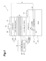
Fig. 1 is a drawing showing a configuration of a light emitting device according to the embodiment. -
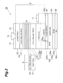
Fig. 2 is a drawing showing a configuration of another light emitting device according to the embodiment. -
Fig. 3 is a drawing illustrating a method of manufacturing an another light emitting device according to the embodiment. -
Fig. 4 is a drawing showing drive current dependence of the degree of polarization according to the embodiment. - Preferred embodiments according to the present invention will be described with reference to the attached drawings. In order to avoid redundancy in description of the drawings, the same elements are designated by the same reference numerals, wherever possible. In
Fig. 1 , a configuration of alight emitting device 1 according to the embodiment is shown. Thelight emitting device 1 comprises acomposite substrate 3, a gallium nitride-basedsemiconductor layer 5, a p-electrode 13, apad electrode 15, and an n-electrode 17. Thecomposite substrate 3 includes abase 19 and a GaNlayer 21. Thebase 19 contains a fluorescent material that emits a fluorescent light component induced by irradiation of a light component emitted from alight emitting layer 9 as described below. The fluorescent material contains a component that emits yellow light having a peak wavelength in a range of not less than 540 nm and not more than 600 nm by absorbing blue light having a peak wavelength in a range of not less than 430 nm and not more than 490 nm. - The GaN
layer 21 is disposed on thebase 19. The GaNlayer 21 is in contact with thebase 19. The GaNlayer 21 has a thickness less than that of the base 19 (hereinafter, "thickness" refers to a width in a direction of a normal line N1 to a principal surface S1 of the GaN layer 21). - The gallium nitride-based
semiconductor layer 5 includes an n-typenitride semiconductor layer 7, alight emitting layer 9, and a p-typenitride semiconductor layer 11. The n-typenitride semiconductor layer 7, thelight emitting layer 9, and the p-typenitride semiconductor layer 11 comprise a hexagonal gallium nitride-based semiconductor. The gallium nitride-basedsemiconductor layer 5 is disposed on the principal surface S1 of theGaN layer 21. The gallium nitride-basedsemiconductor layer 5 is in contact with theGaN layer 21. The gallium nitride-basedsemiconductor layer 5 is deposited by epitaxially growing on the principal surface S1 of theGaN layer 21. - The n-type
nitride semiconductor layer 7 includes aGaN layer 23 and abuffer layer 25. TheGaN layer 23 comprises afirst region 23a and asecond region 23b. Thefirst region 23a and thesecond region 23b are disposed in parallel on the principal surface S1 of theGaN layer 21. Both of thefirst region 23a and thesecond region 23b are in contact with theGaN layer 21. Thebuffer layer 25 is disposed on thefirst region 23a. Thebuffer layer 25 is in contact with thefirst region 23a. Thefirst region 23a, thebuffer layer 25, thelight emitting layer 9, and the p-typenitride semiconductor layer 11 are deposited in sequence on the principal surface S1 of theGaN layer 21. The n-electrode 17 is disposed on thefirst region 23a and is in ohmic contact with thesecond region 23b. Thefirst region 23a has a thickness greater than that of thesecond region 23b. - The
light emitting layer 9 includes barrier layers 27 and well layers 29 which are alternatively deposited to form a multiple quantum well structure. Thelight emitting layer 9 is disposed on thebuffer layer 25. Thelight emitting layer 9 is in contact with thebuffer layer 25. The barrier layers 27 and the well layers 29 are alternatively deposited in a direction orthogonal to the normal line N1. Thelight emitting layer 9 emits blue light having a peak wavelength in a range of not less than 430 nm and not more than 490 nm. - The p-type
nitride semiconductor layer 11 includes an electron-blockinglayer 31 and acontact layer 33. The electron-blockinglayer 31 is disposed on thelight emitting layer 9. The electron-blockinglayer 31 is in contact with thelight emitting layer 9. Thecontact layer 33 is disposed on the electron-blockinglayer 31. Thecontact layer 33 is in contact with the electron-blockinglayer 31. - The p-
electrode 13 is disposed on thecontact layer 33, and is in ohmic contact with thecontact layer 33. Thepad electrode 15 is disposed on the p-electrode 13 and thecontact layer 33. Thepad electrode 15 is in contact with thecontact layer 33 through an apertura of the p-electrode 13. It allows for excellent adhesiveness. - The configuration of the
light emitting device 1 will be described further in detail. Thebase 19 comprises generally polycrystalline ZnSe doped with at least one impurity element selected from the group consisting of aluminum, indium, gallium, chlorine, bromine, and iodine, and preferably polycrystalline ZnSxSe1-x (0 ≤ x ≤ 1) doped with at least one impurity element selected from the group consisting of aluminum, indium, gallium, chlorine, bromine, and iodine. TheGaN layer 21 comprises n-type-doped GaN. TheGaN layer 21 generally has a thickness of about 200 nm, and preferably in a range of not less than 100 nm and not more than 1200 nm. TheGaN layer 21 has a dislocation density of not more than 1×107 cm-2. The angle θ between the normal line N1 to theGaN layer 21 and the c-axis of theGaN layer 21 indicates that the principal surface S1 of theGaN layer 21 is identical to the m-plane of GaN crystal. The angle θ is preferably in a range of not less than 50 degree and not more than 130 degree. - The
GaN layer 23 comprises n-type-doped GaN, and thefirst region 23a has a thickness of about 2 µm. Thebuffer layer 25 comprises n-type-doped InGaN, and has a thickness of about 100 nm. The composition ratios of indium and gallium in thebuffer layer 25 are 0.02 and 0.98, respectively. - The
barrier layer 27 comprises GaN, and has a thickness of about 15 nm. Thewell layer 29 comprises InGaN, and has a thickness of about 3 nm. The composition ratios of indium and gallium in thewell layer 29 are 0.17 and 0.83, respectively. Because the angle θ is in a range of not less than 50 degree and not more than 130 degree, the composition ratio of indium in thewell layer 29 is relatively high, and thus, thelight emitting layer 9 becomes capable of emitting high-intensity blue light. Additionally, because the angle θ is in a range of not less than 50 degree and not more than 130 degree, the piezoelectric field is relatively weak in thelight emitting layer 9, and thus, it allows for a relatively smaller variation width in wavelength of light from thelight emitting layer 9 which is induced by a variation in drive current. - In addition, because the angle θ is in a range of not less than 50 degree and not more than 130 degree, the
light emitting layer 9 emits blue light with an absolute value of the degree of polarization of not less than 0.2. In the embodiment, the degree of polarization is defined by (I1-I2) / (I1+I2), where I1 represents a polarized light component in a direction perpendicular to a direction of the projected c-axis of the hexagonal group-III nitride semiconductor onto a principal surface, and I2 represents a polarized light component in the direction of the projected c-axis of the hexagonal group-III nitride semiconductor onto the principal surface. The polarized light component I1 is larger than the polarized light component I2. - The electron-blocking
layer 31 comprises p-type-doped AlGaN, and has a thickness of about 20 nm. The composition ratios of aluminum and gallium in the electron-blockinglayer 31 are 0.18 and 0.82, respectively. Thecontact layer 33 comprises p-type-doped GaN, and has a thickness of about 50 nm. The p-electrode 13 comprises nickel/gold (Ni/Au), thepad electrode 15 titanium/gold (Ti/Au), and the n-electrode 17 titanium/aluminum (Ti/Al). - An exemplary method of manufacturing the
light emitting device 1 will be described. AGaN layer 21 is processed so as to have the back surface (the surface opposite to the principal surface S1) with an average surface roughness Ra of not more than 1 nm. Abase 19 is compressively bonded to the back surface of theGaN layer 21 under heat to laminate thebase 19 and theGaN layer 21, and thus, acomposite substrate 3 is provided. The back surface of theGaN layer 21 having an average surface roughness Ra of not more than 1 nm results in sufficiently strong lamination of thebase 19 and theGaN layer 21. - Then, a gallium nitride-based
semiconductor layer 5 is formed on the principal surface S1 of theGaN layer 21. An n-type-doped GaN layer (corresponding to a GaN layer 23) is deposited by epitaxy on the principal surface S1 of theGaN layer 21 at a temperature of 840°C into a thickness of about 2 µm. An n-type-doped InGaN layer (corresponding to a buffer layer 25) is deposited by epitaxy on a surface of the GaN layer with a thickness of about 2 µm at a temperature of 840°C into a thickness of about 100 nm. In the n-type-doped InGaN layer, the composition ratios of indium and gallium are 0.02 and 0.98, respectively. Subsequently, a light emitting layer (corresponding to a light emitting layer 9) having a multiple quantum well structure including GaN barrier layers (corresponding to barrier layers 27) and InGaN well layers (corresponding to well layers 29) is deposited by epitaxy on a surface of the InGaN layer with a thickness of about 100 nm. In each of the InGaN well layers, the composition ratios of indium and gallium are 0.17 and 0.83, respectively. Each of the barrier layers is deposited at a temperature of 840°C into a thickness of about 15 nm, and each of the well layers is deposited at a temperature of 780°C into a thickness of about 3 nm. - A p-type-doped AlGaN layer (corresponding to an electron-blocking layer 31) is deposited on the light emitting layer at a temperature of 840°C into a thickness of about 20 nm. In the p-type-doped AlGaN layer, the composition ratios of aluminum and gallium are 0.18 and 0.82, respectively. Subsequently, a p-type-doped GaN layer (corresponding to a contact layer 33) is deposited on the AlGaN layer at a temperature of 840°C into a thickness of about 50 nm. Then, the p-type GaN layer with a thickness of about 50 nm, the p-type AlGaN layer with a thickness of about 20 nm, the light emitting layer, the n-type InGaN layer with a thickness of about 100 nm, and the n-type GaN layer with a thickness of about 2 µm are dry-etched to form the
contact layer 33, the electron-blockinglayer 31, thelight emitting layer 9, thebuffer layer 25, and the GaN layer 23 (afirst region 23a and asecond region 23b). As described above, the gallium nitride-basedsemiconductor layer 5 is deposited by epitaxy on the principal surface S1 of theGaN layer 21. - A p-
electrode 13 is deposited on a surface of thecontact layer 33 by vacuum vapor deposition. And then, apad electrode 15 is deposited on a surface of thecontact layer 33 and a surface of the p-electrode 13 by vacuum vapor deposition, and an n-electrode 17 is deposited on a surface of thesecond region 23b by vacuum vapor deposition. - The
light emitting device 1 fabricated according to the method is operated by current injection. Thelight emitting layer 9 emits blue light having a peak wavelength of 470 nm, while thebase 19, excited by absorption of the blue light from thelight emitting layer 9, emits yellow light. Accordingly, white light obtained by superposition of the blue light and the yellow light is observed. The degree of polarization of the blue light emitted from thelight emitting layer 9 is 0.84. - The
light emitting device 1 can emit white light produced by superposition of blue light directly emitted from thelight emitting layer 9 and yellow light induced by blue light incident on the base 19 from thelight emitting layer 9. Because of the angle θ is in a range of not less than 50 degree and not more than 130 degree, indium content in thelight emitting layer 9 is relatively high, and thus, it allows for emission of high-intensity light. Because the angle θ is in a range of not less than 50 degree and not more than 130 degree, the piezoelectric field is relatively weak, and thus, it allows for a relatively smaller variation width in wavelength of light from thelight emitting layer 9 which is induced by a variation in drive current. The absolute value of the degree of polarization of not less than 0.2 indicates a relatively high degree of polarization. - In
Fig. 2 , a configuration of alight emitting device 1a according to another embodiment is shown. Thelight emitting device 1a includes acomposite substrate 3a in place of thecomposite substrate 3 of thelight emitting device 1 inFig. 1 . Thelight emitting device 1a includes areflective layer 35a. Thelight emitting device 1a has the same configuration as thelight emitting device 1, except for thecomposite substrate 3a and thereflective layer 35a. Thecomposite substrate 3a has abase 19a and aGaN layer 21a. Thebase 19a includes aphosphor layer 37a and asupport layer 39a. Thereflective layer 35a, thephosphor layer 37a, thesupport layer 39a, and theGaN layer 21a are deposited in sequence. Thereflective layer 35a is disposed on the back surface S2 of thephosphor layer 37a. Thereflective layer 35a is in contact with thephosphor layer 37a. Thesupport layer 39a is disposed on a principal surface S3 of thephosphor layer 37a. Thesupport layer 39a is in contact with thephosphor layer 37a. TheGaN layer 21a is disposed on a principal surface S4 of thesupport layer 39a. TheGaN layer 21a is in contact with thesupport layer 39a. - The
reflective layer 35a reflects light emitted from thephosphor layer 37a, and comprises a metal that has high reflectivity (for example, silver). Thephosphor layer 37a, having a thickness sufficient to absorb substantially all blue light incident thereon from alight emitting layer 9, places no limitation on flatness of the interface between thephosphor layer 37a and thereflective layer 35a. On the other hand, thephosphor layer 37a, having a thickness sufficiently less than such a thickness, preferably requires a highly flat interface between thephosphor layer 37a and thereflective layer 35a, so that thereflective layer 35a is a mirror, in order to reduce diffused reflection of blue light generated on the interface between thephosphor layer 37a and thereflective layer 35a, (that is, to avoid a reduction in the degree of polarization of the blue light). - The
phosphor layer 37a, like the base 19, comprises generally polycrystalline ZnSe doped with at least one impurity element selected from the group consisting of aluminum (Al), indium (In), gallium (Ga), chlorine (Cl), bromine (Br), and iodine (I), and preferably polycrystalline ZnSxSe1-x (0 ≤ X ≤ 1) doped with at least one impurity element selected from the group consisting of aluminum, indium, gallium, chlorine, bromine, and iodine. Thesupport layer 39a comprises, for example, monocrystalline sapphire that can sufficiently transmit blue light emitted from thelight emitting layer 9, and can be satisfactorily formed on the GaN layer. - The
GaN layer 21a comprises n-type-doped GaN. TheGaN layer 21a generally has a thickness of about 200 nm, and preferably in a range of not less than 100 nm and not more than 1200 nm. TheGaN layer 21a has a dislocation density of not more than 1×107 cm-2. An angle θa between a normal line N1a to a principal surface S1a of theGaN layer 2 1 a and the c-axis of a GaN crystal of theGaN layer 2 1 a is 105 degrees, which indicates that the principal surface S1a is identical to the (20-2-1) plane of the GaN crystal. The angle θa is preferably in a range of not less than 50 degree and not more than 130 degree. - An exemplary method of manufacturing the
light emitting device 1a will be described. As shown in Part (A) ofFig. 3 , asupport layer 39a is compressively bonded on a principal surface S3 of aphosphor layer 37a under heat to laminate thephosphor layer 37a and thesupport layer 39a, and then aGaN layer 41 is compressively bonded on a principal surface S4 of thesupport layer 39a under heat to laminate thesupport layer 39a and theGaN layer 41. Here, theGaN layer 41 is processed in advance so as to have a surface with an average surface roughness Ra of 1 nm. The surface is made in contact with the principal surface S4 of thesupport layer 39a, and then, thesupport layer 39a and theGaN layer 41 are compressively bonded together under heat to laminate thesupport layer 39a and theGaN layer 41. Accordingly, theGaN layer 41 having an average surface roughness Ra of not more than 1 nm results in sufficiently strong lamination of thesupport layer 39a and theGaN layer 41. - The
GaN layer 41 is cut along a cutting surface L with a wire-saw, as shown in Part (B) ofFig. 3 , to form aGaN layer 21a from theGaN layer 41, as shown in Part (C) ofFig. 3 . The cutting surface L is parallel to the principal surface S3 (or the principal surface S4). Consequently, acomposite substrate 3a including thephosphor layer 37a, thesupport layer 39a, and theGaN layer 21a is formed. - In the same manner as that for the
light emitting device 1, a gallium nitride-basedsemiconductor layer 5 is deposited by epitaxy on the principal surface S1a of theGaN layer 21 a. In addition, a p-electrode 13, apad electrode 15, and an n-electrode 17 are deposited by vacuum vapor deposition. Areflective layer 35a is deposited on the back surface S2 of thephosphor layer 37a by vacuum vapor deposition. - The
light emitting device 1a fabricated according to the method is operated by current injection. Alight emitting layer 9 emits blue light having a peak wavelength of 470 nm, while thephosphor layer 37a, excited by absorption of the blue light from thelight emitting layer 9, emits yellow light. Accordingly, white light obtained by superposition of the blue light and the yellow light is observed. InFig. 4 , observed values of drive current dependence of the degree of polarization of blue light emitted from thelight emitting device 1a is shown. The absolute value of the degree of polarization of the blue light emitted from thelight emitting device 1a in a range of not less than 0.63 (a current of 2 mA) and not more than 0.65 (a current of 500 mA), which indicates a relatively smaller variation in the degree of polarization. Therefore, it is found that thelight emitting device 1a can be used at a wide range of drive currents. - The
light emitting device 1a can emit white light produced by superposition of blue light directly emitted from thelight emitting layer 9 and yellow light induced by blue light incident on thephosphor layer 37a from thelight emitting layer 9. Because the angle θa is in a range of not less than 50 degree and not more than 130 degree, indium content in thelight emitting layer 9 is relatively high, and thus, it allows for emission of high-intensity light. Because the angle θa is in a range of not less than 50 degree and not more than 130 degree, the piezoelectric field is relatively weak, and thus, it allows for a relatively smaller variation width in wavelength of light from thelight emitting layer 9, which is induced by a variation in drive current. The absolute value of the degree of polarization of not less than 0.2 indicates a relatively high degree of polarization. - A light emitting device that emits stable light having a plurality of wavelengths is provided. The light emitting device can emit light produced by superposition of a light component emitted from the light emitting layer and a light component induced by a light component incident on the base from the light emitting layer.
-
- 1, 1a: light emitting device;
- 11: p-type nitride semiconductor layer;
- 13: p-electrode;
- 15: pad electrode;
- 17: n-electrode;
- 19, 19a: base;
- 21, 21a, 23 and 41: GaN layer;
- 23a: first region;
- 23b: second region;
- 25: buffer layer;
- 27: barrier layer;
- 29: well layer;
- 3: composite substrate;
- 31: electron-blocking layer;
- 33: contact layer;
- 35a: reflective layer;
- 37a: phosphor layer;
- 39a: support layer;
- 3a: composite substrate;
- 5: gallium nitride-based semiconductor layer;
- 7: n-type nitride semiconductor layer;
- 9: light emitting layer.
Claims (7)
- A light emitting device comprising:a substrate; anda hexagonal gallium nitride-based semiconductor layer having a light emitting layer which contains indium,the substrate including a base and a gallium nitride layer which has a thickness less than a thickness of the base,the hexagonal gallium nitride-based semiconductor layer being disposed on a principal surface of the gallium nitride layer,an angle between a c-axis of the gallium nitride layer and a normal line to the principal surface of the gallium nitride layer being in a range of not less than 50 degree and not more than 130 degree,the light emitting layer emitting light with an absolute value of the degree of polarization of not less than 0.2,the base containing a fluorescent material that emits a fluorescent light component which is induced by irradiation of a light component emitted from the light emitting layer.
- The light emitting device according to claim 1, wherein the base comprises:a phosphor layer containing the fluorescent material; anda support layer being disposed on a principal surface of the phosphor layer,the gallium nitride layer being disposed on a principal surface of the support layer.
- The light emitting device according to claim 2, further comprising a reflective layer which is disposed on the back surface of the phosphor layer, the reflective layer reflecting light which is emitted from the phosphor layer.
- The light emitting device according to any one of claims 1 to 3, wherein the gallium nitride layer has a thickness in a range of not less than 100 nm and not more than 1200 nm.
- The light emitting device according to any one of claims 1 to 4, wherein the light emitting layer emits light having a peak wavelength in a range of not less than 430 nm and not more than 490 nm.
- The light emitting device according to claim 5, wherein the fluorescent material contains a component that emits light having a peak wavelength in a range of not less than 540 nm and not more than 600 nm.
- The light emitting device according to claim 6, wherein the fluorescent material contains polycrystalline ZnSxSe1-x (0 ≤ x ≤ 1) doped with at least one impurity element selected from the group consisting of aluminum, indium, gallium, chlorine, bromine, and iodine.
Applications Claiming Priority (2)
| Application Number | Priority Date | Filing Date | Title |
|---|---|---|---|
| JP2009228154A JP2011077351A (en) | 2009-09-30 | 2009-09-30 | Light emitting device |
| PCT/JP2010/066554 WO2011040331A1 (en) | 2009-09-30 | 2010-09-24 | Light-emitting element |
Publications (1)
| Publication Number | Publication Date |
|---|---|
| EP2485281A1 true EP2485281A1 (en) | 2012-08-08 |
Family
ID=43779313
Family Applications (1)
| Application Number | Title | Priority Date | Filing Date |
|---|---|---|---|
| EP10807510A Withdrawn EP2485281A1 (en) | 2009-09-30 | 2010-09-24 | Light-emitting element |
Country Status (7)
| Country | Link |
|---|---|
| US (1) | US8823027B2 (en) |
| EP (1) | EP2485281A1 (en) |
| JP (1) | JP2011077351A (en) |
| KR (1) | KR101244470B1 (en) |
| CN (1) | CN102150287B (en) |
| TW (1) | TW201125158A (en) |
| WO (1) | WO2011040331A1 (en) |
Families Citing this family (13)
| Publication number | Priority date | Publication date | Assignee | Title |
|---|---|---|---|---|
| KR20110039313A (en) | 2008-07-07 | 2011-04-15 | 글로 에이비 | Nanostructure LED |
| JP2012243780A (en) * | 2011-05-13 | 2012-12-10 | Toshiba Corp | Semiconductor light-emitting element and wafer |
| CN103165776A (en) * | 2011-12-15 | 2013-06-19 | 南通同方半导体有限公司 | Light-emitting diode structure capable of obtaining three-primary-color light |
| KR20130078345A (en) * | 2011-12-30 | 2013-07-10 | 일진엘이디(주) | Nitride based light emitting device with excellent light efficiency using strain buffer layer |
| JP2013207046A (en) * | 2012-03-28 | 2013-10-07 | Toyoda Gosei Co Ltd | Group iii nitride compound semiconductor light-emitting element and manufacturing method of the same |
| CN103579471B (en) * | 2012-07-23 | 2016-06-15 | 东莞市中镓半导体科技有限公司 | A kind of compound substrate with preventing metal diffusing protective layer |
| EP2824719A4 (en) * | 2012-07-23 | 2016-01-06 | Sino Nitride Semiconductor Co | COMPOSITE SUBSTRATE WITH PROTECTIVE LAYER TO PREVENT METAL DIFFUSION |
| KR101923673B1 (en) | 2012-09-13 | 2018-11-29 | 서울바이오시스 주식회사 | Method of fabricating gallium nitrded based semiconductor device |
| KR102335714B1 (en) * | 2016-10-24 | 2021-12-06 | 글로 에이비 | Light emitting diodes, display elements, and direct-view display elements |
| WO2019240894A1 (en) | 2018-06-14 | 2019-12-19 | Glo Ab | Epitaxial gallium nitride based light emitting diode and method of making thereof |
| CN110752301B (en) * | 2018-07-24 | 2020-11-10 | Tcl科技集团股份有限公司 | Composite material, preparation method thereof and quantum dot light-emitting diode |
| CN111916541A (en) * | 2020-07-29 | 2020-11-10 | 华灿光电(浙江)有限公司 | Light-emitting diode epitaxial wafer and preparation method thereof |
| CN118039759B (en) * | 2024-03-28 | 2024-11-22 | 湘能华磊光电股份有限公司 | Light emitting diode chip and preparation method thereof |
Family Cites Families (20)
| Publication number | Priority date | Publication date | Assignee | Title |
|---|---|---|---|---|
| JP3152170B2 (en) | 1997-06-23 | 2001-04-03 | 昭和電工株式会社 | Compound semiconductor light emitting device |
| JP2000164931A (en) * | 1998-11-27 | 2000-06-16 | Sumitomo Electric Ind Ltd | White light source |
| JP4060511B2 (en) | 2000-03-28 | 2008-03-12 | パイオニア株式会社 | Method for separating nitride semiconductor device |
| US7053413B2 (en) * | 2000-10-23 | 2006-05-30 | General Electric Company | Homoepitaxial gallium-nitride-based light emitting device and method for producing |
| JP3705272B2 (en) | 2003-02-20 | 2005-10-12 | 住友電気工業株式会社 | White light emitting device |
| FR2844099B1 (en) | 2002-09-03 | 2005-09-02 | Commissariat Energie Atomique | SEMICONDUCTOR DEVICE OF QUASI-VERTICAL POWER ON COMPOSITE SUBSTRATE |
| KR100580623B1 (en) * | 2003-08-04 | 2006-05-16 | 삼성전자주식회사 | Semiconductor device having a superlattice semiconductor layer and its manufacturing method |
| US20060006397A1 (en) | 2004-07-09 | 2006-01-12 | Chua Janet B Y | Device and method for emitting output light using group IIA/IIB selenide sulfur-based phosphor material |
| US20060006396A1 (en) | 2004-07-09 | 2006-01-12 | Chua Janet B Y | Phosphor mixture of organge/red ZnSe0.5S0.5:Cu,Cl and green BaSrGa4S7:Eu for white phosphor-converted led |
| US7514721B2 (en) | 2005-11-29 | 2009-04-07 | Koninklijke Philips Electronics N.V. | Luminescent ceramic element for a light emitting device |
| KR100771811B1 (en) * | 2005-12-27 | 2007-10-30 | 삼성전기주식회사 | White light emitting device |
| KR100809209B1 (en) * | 2006-04-25 | 2008-02-29 | 삼성전기주식회사 | Non-polar m-nitride semiconductor manufacturing method |
| JP5003033B2 (en) * | 2006-06-30 | 2012-08-15 | 住友電気工業株式会社 | GaN thin film bonded substrate and manufacturing method thereof, and GaN-based semiconductor device and manufacturing method thereof |
| JP2008159606A (en) | 2006-12-20 | 2008-07-10 | Rohm Co Ltd | Nitride semiconductor light emitting device and manufacturing method thereof |
| US7781783B2 (en) * | 2007-02-07 | 2010-08-24 | SemiLEDs Optoelectronics Co., Ltd. | White light LED device |
| JP2008218645A (en) | 2007-03-02 | 2008-09-18 | Rohm Co Ltd | Light emitting device |
| JP2008235804A (en) | 2007-03-23 | 2008-10-02 | Rohm Co Ltd | Light emitting element |
| JP5201917B2 (en) * | 2007-09-10 | 2013-06-05 | シャープ株式会社 | Air cleaner |
| KR100901369B1 (en) * | 2007-11-19 | 2009-06-05 | 일진반도체 주식회사 | White light emitting diode chip and its manufacturing method |
| US8652948B2 (en) * | 2007-11-21 | 2014-02-18 | Mitsubishi Chemical Corporation | Nitride semiconductor, nitride semiconductor crystal growth method, and nitride semiconductor light emitting element |
-
2009
- 2009-09-30 JP JP2009228154A patent/JP2011077351A/en active Pending
-
2010
- 2010-07-14 US US12/836,199 patent/US8823027B2/en not_active Expired - Fee Related
- 2010-09-24 WO PCT/JP2010/066554 patent/WO2011040331A1/en not_active Ceased
- 2010-09-24 CN CN201080002548.XA patent/CN102150287B/en not_active Expired - Fee Related
- 2010-09-24 EP EP10807510A patent/EP2485281A1/en not_active Withdrawn
- 2010-09-24 KR KR1020117004603A patent/KR101244470B1/en not_active Expired - Fee Related
- 2010-09-30 TW TW099133417A patent/TW201125158A/en unknown
Non-Patent Citations (1)
| Title |
|---|
| See references of WO2011040331A1 * |
Also Published As
| Publication number | Publication date |
|---|---|
| US8823027B2 (en) | 2014-09-02 |
| KR20110053228A (en) | 2011-05-19 |
| TW201125158A (en) | 2011-07-16 |
| CN102150287A (en) | 2011-08-10 |
| CN102150287B (en) | 2014-04-09 |
| US20110073892A1 (en) | 2011-03-31 |
| WO2011040331A1 (en) | 2011-04-07 |
| KR101244470B1 (en) | 2013-03-18 |
| JP2011077351A (en) | 2011-04-14 |
Similar Documents
| Publication | Publication Date | Title |
|---|---|---|
| US8823027B2 (en) | Light emitting device | |
| JP4572270B2 (en) | Nitride semiconductor device and manufacturing method thereof | |
| US7915714B2 (en) | Semiconductor light emitting element and wafer | |
| KR101419105B1 (en) | Light emitting diode, light emitting diode lamp and illuminating device | |
| TWI447956B (en) | Light-emitting diode and manufacturing method thereof and light-emitting diode lamp | |
| WO2011021264A1 (en) | Nitride semiconductor light emitting element | |
| KR20120043149A (en) | Light emitting diode, light emitting diode lamp and lighting device | |
| WO2010116422A1 (en) | Nitride semiconductor light-emitting element, illuminating device, liquid crystal display device, method for producing nitride semiconductor light-emitting element and method for manufacturing illuminating device | |
| KR101377817B1 (en) | Light-emitting diode, light-emitting diode lamp and lighting device | |
| JP2009239075A (en) | Light emitting element | |
| CN102884643B (en) | The group III-nitride light-emitting device of growth on flabby sheaf | |
| JP2008277323A (en) | Semiconductor light emitting device and wafer | |
| JP5586371B2 (en) | Light emitting diode, light emitting diode lamp, and lighting device | |
| JP5047508B2 (en) | Manufacturing method of nitride semiconductor light emitting device | |
| EP1863102A1 (en) | Zinc oxide compound semiconductor light emitting element | |
| JP5557648B2 (en) | Light emitting diode, light emitting diode lamp, and lighting device | |
| KR101637633B1 (en) | Light emitting diode and light emitting diode lamp | |
| JP4917301B2 (en) | Semiconductor light emitting diode | |
| JP2011082248A (en) | Semiconductor light emitting element and method of manufacturing the same, and lamp | |
| JP2019526938A (en) | Optoelectronic element | |
| WO2010113903A1 (en) | Light-emitting element and illuminating device | |
| JP2007081084A (en) | Semiconductor light emitting element |
Legal Events
| Date | Code | Title | Description |
|---|---|---|---|
| PUAI | Public reference made under article 153(3) epc to a published international application that has entered the european phase |
Free format text: ORIGINAL CODE: 0009012 |
|
| 17P | Request for examination filed |
Effective date: 20110215 |
|
| AK | Designated contracting states |
Kind code of ref document: A1 Designated state(s): AL AT BE BG CH CY CZ DE DK EE ES FI FR GB GR HR HU IE IS IT LI LT LU LV MC MK MT NL NO PL PT RO SE SI SK SM TR |
|
| DAX | Request for extension of the european patent (deleted) | ||
| STAA | Information on the status of an ep patent application or granted ep patent |
Free format text: STATUS: THE APPLICATION HAS BEEN WITHDRAWN |
|
| 18W | Application withdrawn |
Effective date: 20150312 |