EP2481511A1 - Gold removal from electronic components - Google Patents
Gold removal from electronic components Download PDFInfo
- Publication number
- EP2481511A1 EP2481511A1 EP11186774A EP11186774A EP2481511A1 EP 2481511 A1 EP2481511 A1 EP 2481511A1 EP 11186774 A EP11186774 A EP 11186774A EP 11186774 A EP11186774 A EP 11186774A EP 2481511 A1 EP2481511 A1 EP 2481511A1
- Authority
- EP
- European Patent Office
- Prior art keywords
- gold
- electronic component
- solder
- electronic components
- cooling
- Prior art date
- Legal status (The legal status is an assumption and is not a legal conclusion. Google has not performed a legal analysis and makes no representation as to the accuracy of the status listed.)
- Granted
Links
Images







Classifications
-
- B—PERFORMING OPERATIONS; TRANSPORTING
- B23—MACHINE TOOLS; METAL-WORKING NOT OTHERWISE PROVIDED FOR
- B23K—SOLDERING OR UNSOLDERING; WELDING; CLADDING OR PLATING BY SOLDERING OR WELDING; CUTTING BY APPLYING HEAT LOCALLY, e.g. FLAME CUTTING; WORKING BY LASER BEAM
- B23K31/00—Processes relevant to this subclass, specially adapted for particular articles or purposes, but not covered by any single one of main groups B23K1/00 - B23K28/00
- B23K31/02—Processes relevant to this subclass, specially adapted for particular articles or purposes, but not covered by any single one of main groups B23K1/00 - B23K28/00 relating to soldering or welding
-
- C—CHEMISTRY; METALLURGY
- C22—METALLURGY; FERROUS OR NON-FERROUS ALLOYS; TREATMENT OF ALLOYS OR NON-FERROUS METALS
- C22B—PRODUCTION AND REFINING OF METALS; PRETREATMENT OF RAW MATERIALS
- C22B11/00—Obtaining noble metals
-
- B—PERFORMING OPERATIONS; TRANSPORTING
- B23—MACHINE TOOLS; METAL-WORKING NOT OTHERWISE PROVIDED FOR
- B23K—SOLDERING OR UNSOLDERING; WELDING; CLADDING OR PLATING BY SOLDERING OR WELDING; CUTTING BY APPLYING HEAT LOCALLY, e.g. FLAME CUTTING; WORKING BY LASER BEAM
- B23K1/00—Soldering, e.g. brazing, or unsoldering
- B23K1/0008—Soldering, e.g. brazing, or unsoldering specially adapted for particular articles or work
- B23K1/0016—Soldering of electronic components
-
- B—PERFORMING OPERATIONS; TRANSPORTING
- B23—MACHINE TOOLS; METAL-WORKING NOT OTHERWISE PROVIDED FOR
- B23K—SOLDERING OR UNSOLDERING; WELDING; CLADDING OR PLATING BY SOLDERING OR WELDING; CUTTING BY APPLYING HEAT LOCALLY, e.g. FLAME CUTTING; WORKING BY LASER BEAM
- B23K1/00—Soldering, e.g. brazing, or unsoldering
- B23K1/20—Preliminary treatment of work or areas to be soldered, e.g. in respect of a galvanic coating
-
- C—CHEMISTRY; METALLURGY
- C22—METALLURGY; FERROUS OR NON-FERROUS ALLOYS; TREATMENT OF ALLOYS OR NON-FERROUS METALS
- C22B—PRODUCTION AND REFINING OF METALS; PRETREATMENT OF RAW MATERIALS
- C22B7/00—Working up raw materials other than ores, e.g. scrap, to produce non-ferrous metals and compounds thereof; Methods of a general interest or applied to the winning of more than two metals
-
- H—ELECTRICITY
- H05—ELECTRIC TECHNIQUES NOT OTHERWISE PROVIDED FOR
- H05K—PRINTED CIRCUITS; CASINGS OR CONSTRUCTIONAL DETAILS OF ELECTRIC APPARATUS; MANUFACTURE OF ASSEMBLAGES OF ELECTRICAL COMPONENTS
- H05K3/00—Apparatus or processes for manufacturing printed circuits
- H05K3/30—Assembling printed circuits with electric components, e.g. with resistors
- H05K3/32—Assembling printed circuits with electric components, e.g. with resistors electrically connecting electric components or wires to printed circuits
- H05K3/34—Assembling printed circuits with electric components, e.g. with resistors electrically connecting electric components or wires to printed circuits by soldering
- H05K3/341—Surface mounted components
-
- H—ELECTRICITY
- H05—ELECTRIC TECHNIQUES NOT OTHERWISE PROVIDED FOR
- H05K—PRINTED CIRCUITS; CASINGS OR CONSTRUCTIONAL DETAILS OF ELECTRIC APPARATUS; MANUFACTURE OF ASSEMBLAGES OF ELECTRICAL COMPONENTS
- H05K2203/00—Indexing scheme relating to apparatus or processes for manufacturing printed circuits covered by H05K3/00
- H05K2203/11—Treatments characterised by their effect, e.g. heating, cooling, roughening
- H05K2203/1105—Heating or thermal processing not related to soldering, firing, curing or laminating, e.g. for shaping the substrate or during finish plating
-
- H—ELECTRICITY
- H05—ELECTRIC TECHNIQUES NOT OTHERWISE PROVIDED FOR
- H05K—PRINTED CIRCUITS; CASINGS OR CONSTRUCTIONAL DETAILS OF ELECTRIC APPARATUS; MANUFACTURE OF ASSEMBLAGES OF ELECTRICAL COMPONENTS
- H05K2203/00—Indexing scheme relating to apparatus or processes for manufacturing printed circuits covered by H05K3/00
- H05K2203/30—Details of processes not otherwise provided for in H05K2203/01 - H05K2203/17
- H05K2203/304—Protecting a component during manufacturing
-
- H—ELECTRICITY
- H05—ELECTRIC TECHNIQUES NOT OTHERWISE PROVIDED FOR
- H05K—PRINTED CIRCUITS; CASINGS OR CONSTRUCTIONAL DETAILS OF ELECTRIC APPARATUS; MANUFACTURE OF ASSEMBLAGES OF ELECTRICAL COMPONENTS
- H05K3/00—Apparatus or processes for manufacturing printed circuits
- H05K3/22—Secondary treatment of printed circuits
-
- H—ELECTRICITY
- H05—ELECTRIC TECHNIQUES NOT OTHERWISE PROVIDED FOR
- H05K—PRINTED CIRCUITS; CASINGS OR CONSTRUCTIONAL DETAILS OF ELECTRIC APPARATUS; MANUFACTURE OF ASSEMBLAGES OF ELECTRICAL COMPONENTS
- H05K3/00—Apparatus or processes for manufacturing printed circuits
- H05K3/30—Assembling printed circuits with electric components, e.g. with resistors
- H05K3/32—Assembling printed circuits with electric components, e.g. with resistors electrically connecting electric components or wires to printed circuits
- H05K3/34—Assembling printed circuits with electric components, e.g. with resistors electrically connecting electric components or wires to printed circuits by soldering
- H05K3/3494—Heating processes for reflow soldering
-
- Y—GENERAL TAGGING OF NEW TECHNOLOGICAL DEVELOPMENTS; GENERAL TAGGING OF CROSS-SECTIONAL TECHNOLOGIES SPANNING OVER SEVERAL SECTIONS OF THE IPC; TECHNICAL SUBJECTS COVERED BY FORMER USPC CROSS-REFERENCE ART COLLECTIONS [XRACs] AND DIGESTS
- Y02—TECHNOLOGIES OR APPLICATIONS FOR MITIGATION OR ADAPTATION AGAINST CLIMATE CHANGE
- Y02P—CLIMATE CHANGE MITIGATION TECHNOLOGIES IN THE PRODUCTION OR PROCESSING OF GOODS
- Y02P70/00—Climate change mitigation technologies in the production process for final industrial or consumer products
- Y02P70/50—Manufacturing or production processes characterised by the final manufactured product
-
- Y—GENERAL TAGGING OF NEW TECHNOLOGICAL DEVELOPMENTS; GENERAL TAGGING OF CROSS-SECTIONAL TECHNOLOGIES SPANNING OVER SEVERAL SECTIONS OF THE IPC; TECHNICAL SUBJECTS COVERED BY FORMER USPC CROSS-REFERENCE ART COLLECTIONS [XRACs] AND DIGESTS
- Y10—TECHNICAL SUBJECTS COVERED BY FORMER USPC
- Y10T—TECHNICAL SUBJECTS COVERED BY FORMER US CLASSIFICATION
- Y10T29/00—Metal working
- Y10T29/49—Method of mechanical manufacture
- Y10T29/49002—Electrical device making
-
- Y—GENERAL TAGGING OF NEW TECHNOLOGICAL DEVELOPMENTS; GENERAL TAGGING OF CROSS-SECTIONAL TECHNOLOGIES SPANNING OVER SEVERAL SECTIONS OF THE IPC; TECHNICAL SUBJECTS COVERED BY FORMER USPC CROSS-REFERENCE ART COLLECTIONS [XRACs] AND DIGESTS
- Y10—TECHNICAL SUBJECTS COVERED BY FORMER USPC
- Y10T—TECHNICAL SUBJECTS COVERED BY FORMER US CLASSIFICATION
- Y10T29/00—Metal working
- Y10T29/49—Method of mechanical manufacture
- Y10T29/49002—Electrical device making
- Y10T29/49117—Conductor or circuit manufacturing
-
- Y—GENERAL TAGGING OF NEW TECHNOLOGICAL DEVELOPMENTS; GENERAL TAGGING OF CROSS-SECTIONAL TECHNOLOGIES SPANNING OVER SEVERAL SECTIONS OF THE IPC; TECHNICAL SUBJECTS COVERED BY FORMER USPC CROSS-REFERENCE ART COLLECTIONS [XRACs] AND DIGESTS
- Y10—TECHNICAL SUBJECTS COVERED BY FORMER USPC
- Y10T—TECHNICAL SUBJECTS COVERED BY FORMER US CLASSIFICATION
- Y10T29/00—Metal working
- Y10T29/49—Method of mechanical manufacture
- Y10T29/49002—Electrical device making
- Y10T29/49117—Conductor or circuit manufacturing
- Y10T29/49124—On flat or curved insulated base, e.g., printed circuit, etc.
- Y10T29/4913—Assembling to base an electrical component, e.g., capacitor, etc.
- Y10T29/49144—Assembling to base an electrical component, e.g., capacitor, etc. by metal fusion
-
- Y—GENERAL TAGGING OF NEW TECHNOLOGICAL DEVELOPMENTS; GENERAL TAGGING OF CROSS-SECTIONAL TECHNOLOGIES SPANNING OVER SEVERAL SECTIONS OF THE IPC; TECHNICAL SUBJECTS COVERED BY FORMER USPC CROSS-REFERENCE ART COLLECTIONS [XRACs] AND DIGESTS
- Y10—TECHNICAL SUBJECTS COVERED BY FORMER USPC
- Y10T—TECHNICAL SUBJECTS COVERED BY FORMER US CLASSIFICATION
- Y10T29/00—Metal working
- Y10T29/49—Method of mechanical manufacture
- Y10T29/49718—Repairing
-
- Y—GENERAL TAGGING OF NEW TECHNOLOGICAL DEVELOPMENTS; GENERAL TAGGING OF CROSS-SECTIONAL TECHNOLOGIES SPANNING OVER SEVERAL SECTIONS OF THE IPC; TECHNICAL SUBJECTS COVERED BY FORMER USPC CROSS-REFERENCE ART COLLECTIONS [XRACs] AND DIGESTS
- Y10—TECHNICAL SUBJECTS COVERED BY FORMER USPC
- Y10T—TECHNICAL SUBJECTS COVERED BY FORMER US CLASSIFICATION
- Y10T29/00—Metal working
- Y10T29/49—Method of mechanical manufacture
- Y10T29/49718—Repairing
- Y10T29/49721—Repairing with disassembling
-
- Y—GENERAL TAGGING OF NEW TECHNOLOGICAL DEVELOPMENTS; GENERAL TAGGING OF CROSS-SECTIONAL TECHNOLOGIES SPANNING OVER SEVERAL SECTIONS OF THE IPC; TECHNICAL SUBJECTS COVERED BY FORMER USPC CROSS-REFERENCE ART COLLECTIONS [XRACs] AND DIGESTS
- Y10—TECHNICAL SUBJECTS COVERED BY FORMER USPC
- Y10T—TECHNICAL SUBJECTS COVERED BY FORMER US CLASSIFICATION
- Y10T29/00—Metal working
- Y10T29/49—Method of mechanical manufacture
- Y10T29/49718—Repairing
- Y10T29/49721—Repairing with disassembling
- Y10T29/49723—Repairing with disassembling including reconditioning of part
- Y10T29/49725—Repairing with disassembling including reconditioning of part by shaping
- Y10T29/49726—Removing material
- Y10T29/49728—Removing material and by a metallurgical operation, e.g., welding, diffusion bonding, casting
Definitions
- Connections on electronic components are typically plated in gold due to the restriction of hazardous substances (i.e., lead) in electrical and electronic equipment.
- the gold plating becomes brittle and can cause the failure of the connections on the electronic components.
- the gold plating is typically removed by dipping the connections on the electronic components in solder pots or hand soldering the connections.
- the dipping of the connections on the electronic components in solder pots and the hand soldering of the connections can cause thermal shock and damage the electronic components.
- One approach provides a method for gold removal from electronic components.
- the method includes (a) forming a gold and solder mixture on the electronic component via a first incrementally controlled heating procedure; (b) incrementally cooling the electronic component via a first cooling procedure; (c) wicking part or all of the gold and solder mixture from the electronic component to a metallic screen via a second incrementally controlled heating procedure; and (d) incrementally cooling the electronic component via a second cooling procedure.
- the step (c) further includes positioning the electronic component on the metallic screen to facilitate transfer of the gold and solder mixture to the metallic screen.
- the step (a) further includes temporarily adhering at least one of solder paste and solder preform to a non-metallic substrate to form a metered solder pad; and positioning the electronic component on the metered solder pad.
- the step (c) further includes depositing flux on the electronic component placed on the metallic screen.
- the method includes (a) automatically unloading a plurality of electronic components from an electronic component holder to individual solder pads adhered to a non-metallic substrate; (b) positioning the non-metallic substrate on a first moving mechanism; (c) moving the non-metallic substrate through a first oven via the first moving mechanism to heat and cool the plurality of electronic components based on a first temperature profile, wherein the heating of each of the solder pads forms a gold and solder mixture on each of the plurality of electronic components; (d) placing the plurality of electronic components on a metallic screen from the non-metallic substrate; (e) loading the metallic screen on a second moving mechanism; and (f) moving the metallic screen through a second oven via the second moving mechanism to heat and cool the plurality of electronic components based on a second temperature profile, wherein the heating of each of the electronic components wicks part or all of the gold and solder mixture to the metallic screen.
- gold in the gold and solder mixture remaining in a solder joint of the electronic component after step (c) is substantially less than 3% gold by volume.
- the method further includes (g) automatically loading the plurality of electronic components into the electronic component holder.
- the non-metallic substrate includes a composite material.
- the metallic screen includes a flux coating to facilitate transfer of the gold and solder mixture to the metallic screen.
- the first incrementally controlled heating procedure has a temperature range of substantially between 0.1 degrees Celsius per second and 3.0 degrees Celsius per second and the first cooling procedure has a temperature range of substantially between 0.1 degrees Celsius per second and 3.0 degrees Celsius per second.
- the second incrementally controlled heating procedure has a temperature range of substantially between 0.1 degrees Celsius per second and 3.0 degrees Celsius per second and the second cooling procedure has a temperature range of substantially between 0.1 degrees Celsius per second and 3.0 degrees Celsius per second.
- the first incrementally controlled heating procedure is substantially the same as the second incrementally controlled heating procedure and the first cooling procedure is substantially the same as the second cooling procedure.
- the gold removal from electronic components technology described herein can provide one or more of the following advantages.
- An advantage to the technology is the gradual heating and/or cooling of the electronic components minimizes thermal stress on the electronic components.
- Another advantage to the technology is the gradual heating and/or cooling of the electronic components increases the useful lifespan of the electronic components.
- Another advantage to the technology is the increased useful lifespan of the electronic components reduces the cost of the devices connected to the electronic components by decreasing the maintenance cost and down-time of the devices.
- Another advantage to the technology is the repeatable and safe method of diluting the gold from the electronic components thereby decreasing the production cost while increasing the useful environments in which the electronic component can be utilized.
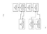
- FIG. 1 is a flowchart of an exemplary process for gold removal from electronic components
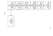
- FIG. 2 is a flowchart of another exemplary process for gold removal from electronic components
- FIG. 3 is a flowchart of an exemplary process for electronic thermal shock management
- FIG. 4 is a block diagram of an exemplary metered solder pad
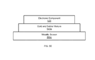
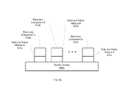
- FIGS. 5A-5E are block diagrams illustrating an exemplary process for gold removal from an electronic component.
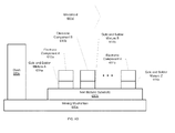
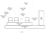
- FIGS. 6A-6H are block diagrams illustrating an exemplary process for gold removal from electronic components.
- the gold removal from electronic components technology described herein enables the gradual heating and/or cooling of the electronic components to minimize damage and prolong the useful life of the electronic components.
- the technology includes the placement of solder paste and/or printed solder pads on a non-metallic substrate.
- the gold plated electronic components are automatically or manually placed on the printed solder pads.
- the printed solder pads are then mass reflowed (heated and/or cooled) to form a solder/gold mix on the printed solder pads.
- the printed solder pads are then placed on a fluxed metallic screen.
- the fluxed metallic screen is then mass reflowed (heated and/or cooled) and the solder/gold mix wicks (e.g., capillary force, absorption force, etc.) to the hot fluxed metallic screen, thereby clearing the electronic component of the gold plating and replacing the gold plating with a solder/gold mix.
- the gold on the electronic components is advantageously diluted and removed to prevent gold embrittlement of the solder joint on the electronic component (e.g., removing the gold to five micrometers on the electronic component, removing the gold to five to ten micrometers on the electronic component, etc.)
- FIG. 1 is a flowchart 100 of an exemplary process for gold removal from electronic components.
- the process includes forming (110) a gold and solder mixture (e.g., 60% gold and 40% solder, 40% gold and 60% solder, etc.) on the electronic component (e.g., surface-mount technology component, integrated circuit component, leadless electronic component, etc.) via a first incrementally controlled heating procedure (e.g., + 2.0° Celsius per second heating, + 200° Celsius per minute heating, etc.).
- the first heating procedure advantageously enables the electronic component to be heated in a controlled fashion (i.e., in a temperature controlled environment), thereby minimizing thermal stress on the electronic components and maximizing the useful life of the electronic component.
- the process further includes incrementally cooling (120) the electronic component via a first cooling procedure (e.g., -1.0° Celsius per second cooling, -100° Celsius per minute cooling, etc.).
- the first cooling procedure advantageously enables the electronic component to be cooled in a controlled fashion (i.e., in a temperature controlled environment), thereby minimizing thermal stress on the electronic components and maximizing the useful life of the electronic component.
- the process further includes wicking (130) part or all of the gold and solder mixture from the electronic component to a metallic screen (e.g., copper, iron, etc.), via a second incrementally controlled heating procedure (e.g., + 3.0° Celsius per second heating, + 400° Celsius per minute heating, etc.).
- the second heating procedure advantageously enables the electronic component to be heated in a controlled fashion (i.e., in a temperature controlled environment), thereby minimizing thermal stress on the electronic components and maximizing the useful life of the electronic component.
- the part or all of the gold and solder mixture is attracted to the metallic screen due to a capillary force between the gold and solder mixture and metallic screen.
- the metallic screen is advantageously a carrier to absorb the gold and solder mixture from the electronic component.
- the process further includes incrementally cooling (140) the electronic component via a second cooling procedure (e.g., -2.0° Celsius per second cooling, -400° Celsius per minute cooling, etc.).
- the second cooling procedure advantageously enables the electronic component to be cooled in a controlled fashion (i.e., in a temperature controlled environment), thereby minimizing thermal stress on the electronic components and maximizing the useful life of the electronic component.
- the process describes the first heating procedure, the first cooling procedure, the second heating procedure, and the second cooling procedure, the process can include any number and/or type of heating and/or cooling techniques.
- the process includes a steady state heating of +1.0° Celsius per second throughout the process and a steady state cooling of -2.0° Celsius per second throughout the process.
- the process includes a heating of +1.0° Celsius per second with an incremental increase of +2.0° Celsius per hour throughout the process and a steady state cooling of -2.0° Celsius per second with an incremental decrease of -0.5° Celsius per hour cooling throughout the process.
- the process includes temporarily adhering (112) at least one of solder paste and solder perform to a non-metallic substrate to form a metered solder pad (e.g., stone, synthetic material, etc.).
- a metered solder pad e.g., stone, synthetic material, etc.
- the process includes positioning (114) the electronic component on the metered solder pad.
- the positioning (114) of the electronic component can, for example, be performed by an operator (e.g., directly, indirectly, etc.) and/or an automated positioning mechanism (e.g., robot, factory machine, etc.).
- the process includes positioning (132) the electronic component on the metallic screen to facilitate transfer of the gold and solder mixture to the metallic screen.
- the metallic screen can be, for example, a solder absorbing screen, a solder wicking screen, and/or any other type of metallic screen.
- the process includes positioning the electronic component on a first metallic screen to facilitate absorption of the gold and solder mixture to the first metallic screen and positioning the electronic component on a second metallic screen to facilitate wicking of the gold and solder mixture to the second metallic screen.
- the non-metallic substrate comprises a composite material (e.g., woven carbon fiber, metal matrix material, etc.).
- the metallic screen includes a flux coating to facilitate transfer of the gold and solder mixture to the metallic screen.
- the flux coating can, for example, remove surface oxidation on the electronic component and/or facilitate the removal of the gold.
- the process is performed in a nitrogen environment (e.g., nitrogen filled container, nitrogen stream blown on the electronic component, etc.).
- the first incrementally controlled heating procedure has a temperature range of substantially between 0.1 degrees Celsius per second and 3.0 degrees Celsius per second and the first cooling procedure has a temperature range of substantially between 0.1 degrees Celsius per second and 3.0 degrees Celsius per second.
- this example illustrates temperature ranges for the heating procedure and the cooling procedure, the technology described herein can utilize any controlled heating/cooling procedures (e.g., 0.001 degrees Celsius per second, ⁇ 10.0 degrees Celsius, etc.).
- Table 1 illustrates an exemplary heating procedure and cooling procedure. Table 1.
- the second incrementally controlled heating procedure has a temperature range of substantially between 0.1 degrees Celsius per second and 3.0 degrees Celsius per second and the second cooling procedure has a temperature range of substantially between 0.1 degrees Celsius per second and 3.0 degrees Celsius per second.
- this example illustrates temperature ranges for the heating procedure and the cooling procedure, the technology described herein can utilize any controlled heating/cooling procedures (e.g., 4.0 degrees Celsius per second, 10.0 degrees Celsius per second, 0.00001 degrees Celsius per second, ⁇ 50.0 degrees Celsius, etc.).
- Table 2 illustrates another exemplary heating procedure and cooling procedure. Table 2.
- the first incrementally controlled heating procedure is substantially the same as the second incrementally controlled heating procedure and the first cooling procedure is substantially the same as the second cooling procedure.
- gold in the gold and solder mixture remaining in a solder joint of the electronic component after the wicking of part or all of the gold and solder mixture from the electronic component to the metallic screen is substantially less than 3% gold by volume (e.g., ⁇ 1.0%, ⁇ 0.001%, etc.). The reduction of the gold and solder mixture to substantially less than 3% gold by volume advantageously dilutes and removes the gold to a level that substantially prevents gold embrittlement of the solder joint on the electronic component.
- FIG. 2 is a flowchart 200 of another exemplary process for gold removal from electronic components.
- the process includes forming (210) a gold and solder mixture on the electronic component via a first incrementally controlled heating procedure.
- the process further includes incrementally cooling (220) the electronic component via a first cooling procedure.
- the process further includes wicking (230) part or all of the gold and solder mixture from the electronic component to a metallic screen via a second incrementally controlled heating procedure.
- the process further includes incrementally cooling (240) the electronic component via a second cooling procedure.
- the process further includes depositing (232) flux on the electronic component placed on the metallic screen.
- the heating and cooling procedures described in this exemplary process can utilize any of the examples and/or techniques as described herein.
- the high temperature of the heating procedure described in this exemplary process is the melting temperature of the solder.
- FIG. 3 is a flowchart 300 of an exemplary process for electronic thermal shock management.
- the process includes automatically unloading (310) a plurality of electronic components from an electronic component holder (e.g., tape of components, package of components, stick of components, etc.) to individual solder pads adhered to a non-metallic substrate.
- the process further includes positioning (320) the non-metallic substrate on a first moving mechanism.
- the process further includes moving (330) the non-metallic substrate through a first oven (e.g., reflow oven, multi-zone reflow oven, hot plate device, hot air device, etc.) via the first moving mechanism to heat and cool the plurality of electronic components based on a first temperature profile.
- the heating of each of the solder pads forms a gold and solder mixture on each of the plurality of electronic components.
- the process further includes placing (340) the plurality of electronic components on a metallic screen from the non-metallic substrate.
- the process further includes loading (350) the metallic screen on a second moving mechanism.
- the process further includes moving (360) the metallic screen through a second oven via the second moving mechanism to heat and cool the plurality of electronic components based on a second temperature profile.
- the heating of each of the electronic components wicks part or all of the gold and solder mixture to the metallic screen.
- the process further includes automatically loading (370) the plurality of electronic components into the electronic component holder.
- the heating and cooling profiles described in this exemplary process can utilize any of the examples and/or techniques as described herein. In other examples, the high temperature of the heating profiles described in this exemplary process is the melting temperature of the solder pads.
- Table 3 illustrates exemplary oven zones associated with another exemplary heating procedure and cooling profiles.
- Exemplary Heating and Cooling Profiles Oven Zone Time Start Temperature End Temperature Increase/Decrease 1 0 seconds through 57 seconds 18° Celsius 75° Celsius + 1.0° Celsius per second (Heating) 2 58 seconds through 158 seconds 75° Celsius 225° Celsius + 1.5° Celsius per second (Heating) 5 159 seconds through 262.5 seconds 225° Celsius 18° Celsius - 2.0 ° Celsius per second (Cooling) 6 263 seconds through 470 seconds 18° Celsius 225° Celsius + 1.0° Celsius per second (Heating) 10 471 seconds through 533.5 seconds 225° Celsius 100° Celsius - 2.0 ° Celsius per second (Cooling) 11 534 seconds through 616 seconds 100° Celsius 18° Celsius - 1.0 ° Celsius per second (Cooling)
- FIG. 4 is a block diagram of an exemplary metered solder pad 400.
- the metered solder pad 400 includes a non-metallic substrate 410 and a plurality of electronic components A 420a, B 420b, C 420c, D 420d, E 420e, and F 420f.
- FIGS. 5A-5E are block diagrams illustrating an exemplary process for gold removal from an electronic component.
- FIG. 5A illustrates an exemplary solder paste and/or solder preform 530a temporarily adhered to a non-metallic substrate 510 (also referred to as forming a metered solder pad).
- An electronic component 520 is positioned on the solder paste and/or solder preform 530a.
- FIG. 5B illustrates a gold and solder mixture 540b formed on the non-metallic substrate 510 via a first incrementally controlled heating procedure.
- FIG. 5C illustrates the electronic component 520 and the gold and solder mixture 540b placed on a metallic screen 550c.
- FIG. 5D illustrates flux 560d deposited on the metallic screen 550c.
- FIG. 5E illustrates part or all of the gold and solder mixture 540e from the electronic component wicked to the metallic screen 550c via a second incrementally controlled heating procedure.
- FIGS. 6A-6H are block diagrams illustrating an exemplary process for gold removal from electronic components.
- FIG. 6A illustrates an electronic component holder 610a holding a plurality of electronic components A 610a, B 610b through Z 610z (generally referred to as electronic components 610).
- FIG. 6B illustrates the electronic components 610 placed on individual solder pads A 612a, B 612b through Z 612z, respectively (generally referred to as solder pads 612), on a non-metallic substrate 630b.
- FIG. 6C illustrates the non-metallic substrate 630b positioned on a moving mechanism 640c and movement (604c) of the non-metallic substrate 630b through an oven 650c.
- FIG. 6D illustrates the non-metallic substrate 630b after movement (604d) through the oven 650c. As illustrated in FIG. 6D , the heating of the solder pads 612 forms a gold and solder mixture A 614a, B 614b through Z 614z (generally referred to as gold and solder mixture 614) on the non-metallic substrate 630b, respectively.
- FIG. 6E illustrates the electronic components 610 and the gold and solder mixture 614 placed on a metallic screen 660e.
- FIG. 6F illustrates the metallic screen 660e loaded on a moving mechanism 670f.
- FIG. 6G illustrates movement (606g) of the metallic screen 660e through an oven 680g.
- FIG. 6H illustrates the metallic screen 660e after movement (606h) through the oven 680g.
- the heating of the electronic components 610 and the gold and solder mixture 614 wicks the gold and solder mixture A 616a, B 616b through Z 616z to the metallic screen 660e.
- Comprise, include, and/or plural forms of each are open ended and include the listed parts and can include additional parts that are not listed. And/or is open ended and includes one or more of the listed parts and combinations of the listed parts.
Landscapes
- Engineering & Computer Science (AREA)
- Mechanical Engineering (AREA)
- Manufacturing & Machinery (AREA)
- Chemical & Material Sciences (AREA)
- Microelectronics & Electronic Packaging (AREA)
- Materials Engineering (AREA)
- Metallurgy (AREA)
- Organic Chemistry (AREA)
- General Life Sciences & Earth Sciences (AREA)
- Geology (AREA)
- Environmental & Geological Engineering (AREA)
- Life Sciences & Earth Sciences (AREA)
- Electric Connection Of Electric Components To Printed Circuits (AREA)
Abstract
Description
- Connections on electronic components are typically plated in gold due to the restriction of hazardous substances (i.e., lead) in electrical and electronic equipment. However, in some environments, the gold plating becomes brittle and can cause the failure of the connections on the electronic components. The gold plating is typically removed by dipping the connections on the electronic components in solder pots or hand soldering the connections. However, the dipping of the connections on the electronic components in solder pots and the hand soldering of the connections can cause thermal shock and damage the electronic components. Thus, a need exists in the art for gold removal from connections on the electronic components with the features as described herein.
- One approach provides a method for gold removal from electronic components. The method includes (a) forming a gold and solder mixture on the electronic component via a first incrementally controlled heating procedure; (b) incrementally cooling the electronic component via a first cooling procedure; (c) wicking part or all of the gold and solder mixture from the electronic component to a metallic screen via a second incrementally controlled heating procedure; and (d) incrementally cooling the electronic component via a second cooling procedure. In some examples, the step (c) further includes positioning the electronic component on the metallic screen to facilitate transfer of the gold and solder mixture to the metallic screen. In other examples, the step (a) further includes temporarily adhering at least one of solder paste and solder preform to a non-metallic substrate to form a metered solder pad; and positioning the electronic component on the metered solder pad. In other examples, the step (c) further includes depositing flux on the electronic component placed on the metallic screen.
- Another approach provides a method for electronic thermal shock management. The method includes (a) automatically unloading a plurality of electronic components from an electronic component holder to individual solder pads adhered to a non-metallic substrate; (b) positioning the non-metallic substrate on a first moving mechanism; (c) moving the non-metallic substrate through a first oven via the first moving mechanism to heat and cool the plurality of electronic components based on a first temperature profile, wherein the heating of each of the solder pads forms a gold and solder mixture on each of the plurality of electronic components; (d) placing the plurality of electronic components on a metallic screen from the non-metallic substrate; (e) loading the metallic screen on a second moving mechanism; and (f) moving the metallic screen through a second oven via the second moving mechanism to heat and cool the plurality of electronic components based on a second temperature profile, wherein the heating of each of the electronic components wicks part or all of the gold and solder mixture to the metallic screen. In some examples, gold in the gold and solder mixture remaining in a solder joint of the electronic component after step (c) is substantially less than 3% gold by volume. In other examples, the method further includes (g) automatically loading the plurality of electronic components into the electronic component holder.
- Any of the approaches described herein can include one or more of the following examples.
- In some examples, the non-metallic substrate includes a composite material.
- In some examples, the metallic screen includes a flux coating to facilitate transfer of the gold and solder mixture to the metallic screen.
- In other examples, the first incrementally controlled heating procedure has a temperature range of substantially between 0.1 degrees Celsius per second and 3.0 degrees Celsius per second and the first cooling procedure has a temperature range of substantially between 0.1 degrees Celsius per second and 3.0 degrees Celsius per second.
- In some examples, the second incrementally controlled heating procedure has a temperature range of substantially between 0.1 degrees Celsius per second and 3.0 degrees Celsius per second and the second cooling procedure has a temperature range of substantially between 0.1 degrees Celsius per second and 3.0 degrees Celsius per second.
- In other examples, the first incrementally controlled heating procedure is substantially the same as the second incrementally controlled heating procedure and the first cooling procedure is substantially the same as the second cooling procedure.
- The gold removal from electronic components technology described herein can provide one or more of the following advantages. An advantage to the technology is the gradual heating and/or cooling of the electronic components minimizes thermal stress on the electronic components. Another advantage to the technology is the gradual heating and/or cooling of the electronic components increases the useful lifespan of the electronic components.
- Another advantage to the technology is the increased useful lifespan of the electronic components reduces the cost of the devices connected to the electronic components by decreasing the maintenance cost and down-time of the devices. Another advantage to the technology is the repeatable and safe method of diluting the gold from the electronic components thereby decreasing the production cost while increasing the useful environments in which the electronic component can be utilized.
- The foregoing and other objects, features and advantages will be apparent from the following more particular description of the embodiments, as illustrated in the accompanying drawings in which like reference characters refer to the same parts throughout the different views. The drawings are not necessarily to scale, emphasis instead being placed upon illustrating the principles of the embodiments.
-
FIG. 1 is a flowchart of an exemplary process for gold removal from electronic components; -
FIG. 2 is a flowchart of another exemplary process for gold removal from electronic components; -
FIG. 3 is a flowchart of an exemplary process for electronic thermal shock management; -
FIG. 4 is a block diagram of an exemplary metered solder pad; -
FIGS. 5A-5E are block diagrams illustrating an exemplary process for gold removal from an electronic component; and -
FIGS. 6A-6H are block diagrams illustrating an exemplary process for gold removal from electronic components. - The gold removal from electronic components technology described herein enables the gradual heating and/or cooling of the electronic components to minimize damage and prolong the useful life of the electronic components. The technology includes the placement of solder paste and/or printed solder pads on a non-metallic substrate. The gold plated electronic components are automatically or manually placed on the printed solder pads. The printed solder pads are then mass reflowed (heated and/or cooled) to form a solder/gold mix on the printed solder pads. The printed solder pads are then placed on a fluxed metallic screen. The fluxed metallic screen is then mass reflowed (heated and/or cooled) and the solder/gold mix wicks (e.g., capillary force, absorption force, etc.) to the hot fluxed metallic screen, thereby clearing the electronic component of the gold plating and replacing the gold plating with a solder/gold mix. The gold on the electronic components is advantageously diluted and removed to prevent gold embrittlement of the solder joint on the electronic component (e.g., removing the gold to five micrometers on the electronic component, removing the gold to five to ten micrometers on the electronic component, etc.)
-
FIG. 1 is aflowchart 100 of an exemplary process for gold removal from electronic components. The process includes forming (110) a gold and solder mixture (e.g., 60% gold and 40% solder, 40% gold and 60% solder, etc.) on the electronic component (e.g., surface-mount technology component, integrated circuit component, leadless electronic component, etc.) via a first incrementally controlled heating procedure (e.g., + 2.0° Celsius per second heating, + 200° Celsius per minute heating, etc.). The first heating procedure advantageously enables the electronic component to be heated in a controlled fashion (i.e., in a temperature controlled environment), thereby minimizing thermal stress on the electronic components and maximizing the useful life of the electronic component. The process further includes incrementally cooling (120) the electronic component via a first cooling procedure (e.g., -1.0° Celsius per second cooling, -100° Celsius per minute cooling, etc.). The first cooling procedure advantageously enables the electronic component to be cooled in a controlled fashion (i.e., in a temperature controlled environment), thereby minimizing thermal stress on the electronic components and maximizing the useful life of the electronic component. - The process further includes wicking (130) part or all of the gold and solder mixture from the electronic component to a metallic screen (e.g., copper, iron, etc.), via a second incrementally controlled heating procedure (e.g., + 3.0° Celsius per second heating, + 400° Celsius per minute heating, etc.). The second heating procedure advantageously enables the electronic component to be heated in a controlled fashion (i.e., in a temperature controlled environment), thereby minimizing thermal stress on the electronic components and maximizing the useful life of the electronic component. The part or all of the gold and solder mixture is attracted to the metallic screen due to a capillary force between the gold and solder mixture and metallic screen. In other words, the metallic screen is advantageously a carrier to absorb the gold and solder mixture from the electronic component. Although the process is described as utilizing the metallic screen, any other type of material that provides for the capillary force can be utilized in the process.
- The process further includes incrementally cooling (140) the electronic component via a second cooling procedure (e.g., -2.0° Celsius per second cooling, -400° Celsius per minute cooling, etc.). The second cooling procedure advantageously enables the electronic component to be cooled in a controlled fashion (i.e., in a temperature controlled environment), thereby minimizing thermal stress on the electronic components and maximizing the useful life of the electronic component. Although the process describes the first heating procedure, the first cooling procedure, the second heating procedure, and the second cooling procedure, the process can include any number and/or type of heating and/or cooling techniques. For example, the process includes a steady state heating of +1.0° Celsius per second throughout the process and a steady state cooling of -2.0° Celsius per second throughout the process. As another example, the process includes a heating of +1.0° Celsius per second with an incremental increase of +2.0° Celsius per hour throughout the process and a steady state cooling of -2.0° Celsius per second with an incremental decrease of -0.5° Celsius per hour cooling throughout the process.
- In some examples, the process includes temporarily adhering (112) at least one of solder paste and solder perform to a non-metallic substrate to form a metered solder pad (e.g., stone, synthetic material, etc.). In other examples, the process includes positioning (114) the electronic component on the metered solder pad. The positioning (114) of the electronic component can, for example, be performed by an operator (e.g., directly, indirectly, etc.) and/or an automated positioning mechanism (e.g., robot, factory machine, etc.).
- In other examples, the process includes positioning (132) the electronic component on the metallic screen to facilitate transfer of the gold and solder mixture to the metallic screen. The metallic screen can be, for example, a solder absorbing screen, a solder wicking screen, and/or any other type of metallic screen. In some examples, the process includes positioning the electronic component on a first metallic screen to facilitate absorption of the gold and solder mixture to the first metallic screen and positioning the electronic component on a second metallic screen to facilitate wicking of the gold and solder mixture to the second metallic screen.
- In some examples, the non-metallic substrate comprises a composite material (e.g., woven carbon fiber, metal matrix material, etc.). In other examples, the metallic screen includes a flux coating to facilitate transfer of the gold and solder mixture to the metallic screen. The flux coating can, for example, remove surface oxidation on the electronic component and/or facilitate the removal of the gold. In some examples, the process is performed in a nitrogen environment (e.g., nitrogen filled container, nitrogen stream blown on the electronic component, etc.).
- In some examples, the first incrementally controlled heating procedure has a temperature range of substantially between 0.1 degrees Celsius per second and 3.0 degrees Celsius per second and the first cooling procedure has a temperature range of substantially between 0.1 degrees Celsius per second and 3.0 degrees Celsius per second. Although this example illustrates temperature ranges for the heating procedure and the cooling procedure, the technology described herein can utilize any controlled heating/cooling procedures (e.g., 0.001 degrees Celsius per second, ± 10.0 degrees Celsius, etc.). Table 1 illustrates an exemplary heating procedure and cooling procedure.
Table 1. Exemplary Heating and Cooling Procedures Time Start Temperature End Temperature Increase/Decrease 0 seconds through 18° Celsius 118° Celsius + 2.0° Celsius per 50 seconds second (Heating) 50 seconds through 118° Celsius 230° Celsius + 3.0° Celsius per 87 seconds second (Heating) 88 seconds through 143 seconds 230° Celsius 175° Celsius - 1.0° Celsius per second (Cooling) 144 seconds through 222.5 seconds 175° Celsius 18° Celsius - 2.0° Celsius per second (Cooling) - In other examples, the second incrementally controlled heating procedure has a temperature range of substantially between 0.1 degrees Celsius per second and 3.0 degrees Celsius per second and the second cooling procedure has a temperature range of substantially between 0.1 degrees Celsius per second and 3.0 degrees Celsius per second. Although this example illustrates temperature ranges for the heating procedure and the cooling procedure, the technology described herein can utilize any controlled heating/cooling procedures (e.g., 4.0 degrees Celsius per second, 10.0 degrees Celsius per second, 0.00001 degrees Celsius per second, ± 50.0 degrees Celsius, etc.). Table 2 illustrates another exemplary heating procedure and cooling procedure.
Table 2. Exemplary Heating and Cooling Procedures Time Start Temperature End Temperature Increase/Decrease 0 seconds through 15° Celsius 125° Celsius + 1.0° Celsius per 115 seconds second (Heating) 116 seconds 125° Celsius 160° Celsius + 1.5° Celsius per through 139 seconds second (Heating) 140 seconds 160° Celsius 15° Celsius - 2.0° Celsius per through 212.5 seconds second (Cooling) - In some examples, the first incrementally controlled heating procedure is substantially the same as the second incrementally controlled heating procedure and the first cooling procedure is substantially the same as the second cooling procedure. In other examples, gold in the gold and solder mixture remaining in a solder joint of the electronic component after the wicking of part or all of the gold and solder mixture from the electronic component to the metallic screen is substantially less than 3% gold by volume (e.g., ±1.0%, ±0.001%, etc.). The reduction of the gold and solder mixture to substantially less than 3% gold by volume advantageously dilutes and removes the gold to a level that substantially prevents gold embrittlement of the solder joint on the electronic component.
-
FIG. 2 is aflowchart 200 of another exemplary process for gold removal from electronic components. The process includes forming (210) a gold and solder mixture on the electronic component via a first incrementally controlled heating procedure. The process further includes incrementally cooling (220) the electronic component via a first cooling procedure. The process further includes wicking (230) part or all of the gold and solder mixture from the electronic component to a metallic screen via a second incrementally controlled heating procedure. The process further includes incrementally cooling (240) the electronic component via a second cooling procedure. In some examples, the process further includes depositing (232) flux on the electronic component placed on the metallic screen. The heating and cooling procedures described in this exemplary process can utilize any of the examples and/or techniques as described herein. In some examples, the high temperature of the heating procedure described in this exemplary process is the melting temperature of the solder. -
FIG. 3 is aflowchart 300 of an exemplary process for electronic thermal shock management. The process includes automatically unloading (310) a plurality of electronic components from an electronic component holder (e.g., tape of components, package of components, stick of components, etc.) to individual solder pads adhered to a non-metallic substrate. The process further includes positioning (320) the non-metallic substrate on a first moving mechanism. The process further includes moving (330) the non-metallic substrate through a first oven (e.g., reflow oven, multi-zone reflow oven, hot plate device, hot air device, etc.) via the first moving mechanism to heat and cool the plurality of electronic components based on a first temperature profile. The heating of each of the solder pads forms a gold and solder mixture on each of the plurality of electronic components. - The process further includes placing (340) the plurality of electronic components on a metallic screen from the non-metallic substrate. The process further includes loading (350) the metallic screen on a second moving mechanism. The process further includes moving (360) the metallic screen through a second oven via the second moving mechanism to heat and cool the plurality of electronic components based on a second temperature profile. The heating of each of the electronic components wicks part or all of the gold and solder mixture to the metallic screen. In some examples, the process further includes automatically loading (370) the plurality of electronic components into the electronic component holder. The heating and cooling profiles described in this exemplary process can utilize any of the examples and/or techniques as described herein. In other examples, the high temperature of the heating profiles described in this exemplary process is the melting temperature of the solder pads. Table 3 illustrates exemplary oven zones associated with another exemplary heating procedure and cooling profiles.
Table 3. Exemplary Heating and Cooling Profiles Oven Zone Time Start Temperature End Temperature Increase/ Decrease 1 0 seconds through 57 seconds 18° Celsius 75° Celsius + 1.0° Celsius per second (Heating) 2 58 seconds through 158 seconds 75° Celsius 225° Celsius + 1.5° Celsius per second (Heating) 5 159 seconds through 262.5 seconds 225° Celsius 18° Celsius - 2.0 ° Celsius per second (Cooling) 6 263 seconds through 470 seconds 18° Celsius 225° Celsius + 1.0° Celsius per second (Heating) 10 471 seconds through 533.5 seconds 225° Celsius 100° Celsius - 2.0 ° Celsius per second (Cooling) 11 534 seconds through 616 seconds 100° Celsius 18° Celsius - 1.0 ° Celsius per second (Cooling) -
FIG. 4 is a block diagram of an exemplarymetered solder pad 400. Themetered solder pad 400 includes anon-metallic substrate 410 and a plurality of electronic components A 420a,B 420b,C 420c, D 420d,E 420e, andF 420f. -
FIGS. 5A-5E are block diagrams illustrating an exemplary process for gold removal from an electronic component.FIG. 5A illustrates an exemplary solder paste and/orsolder preform 530a temporarily adhered to a non-metallic substrate 510 (also referred to as forming a metered solder pad). Anelectronic component 520 is positioned on the solder paste and/orsolder preform 530a.FIG. 5B illustrates a gold andsolder mixture 540b formed on thenon-metallic substrate 510 via a first incrementally controlled heating procedure.FIG. 5C illustrates theelectronic component 520 and the gold andsolder mixture 540b placed on ametallic screen 550c.FIG. 5D illustratesflux 560d deposited on themetallic screen 550c.FIG. 5E illustrates part or all of the gold andsolder mixture 540e from the electronic component wicked to themetallic screen 550c via a second incrementally controlled heating procedure. -
FIGS. 6A-6H are block diagrams illustrating an exemplary process for gold removal from electronic components.FIG. 6A illustrates anelectronic component holder 610a holding a plurality of electronic components A 610a,B 610b throughZ 610z (generally referred to as electronic components 610).FIG. 6B illustrates the electronic components 610 placed on individual solder pads A 612a,B 612b throughZ 612z, respectively (generally referred to as solder pads 612), on anon-metallic substrate 630b.FIG. 6C illustrates thenon-metallic substrate 630b positioned on a movingmechanism 640c and movement (604c) of thenon-metallic substrate 630b through anoven 650c.FIG. 6D illustrates thenon-metallic substrate 630b after movement (604d) through theoven 650c. As illustrated inFIG. 6D , the heating of the solder pads 612 forms a gold andsolder mixture A 614a,B 614b throughZ 614z (generally referred to as gold and solder mixture 614) on thenon-metallic substrate 630b, respectively. -
FIG. 6E illustrates the electronic components 610 and the gold and solder mixture 614 placed on ametallic screen 660e.FIG. 6F illustrates themetallic screen 660e loaded on a movingmechanism 670f.FIG. 6G illustrates movement (606g) of themetallic screen 660e through anoven 680g.FIG. 6H illustrates themetallic screen 660e after movement (606h) through theoven 680g. As illustrated inFIG. 6H , the heating of the electronic components 610 and the gold and solder mixture 614 wicks the gold andsolder mixture A 616a, B 616b throughZ 616z to themetallic screen 660e. - Comprise, include, and/or plural forms of each are open ended and include the listed parts and can include additional parts that are not listed. And/or is open ended and includes one or more of the listed parts and combinations of the listed parts.
- One skilled in the art will realize the invention may be embodied in other specific forms without departing from the spirit or essential characteristics thereof. The foregoing embodiments are therefore to be considered in all respects illustrative rather than limiting of the invention described herein. Scope of the invention is thus indicated by the appended claims, rather than by the foregoing description, and all changes that come within the meaning and range of equivalency of the claims are therefore intended to be embraced therein.
Claims (12)
- A method for removing gold plating on an electronic component, the method comprising:(a) forming a gold and solder mixture on the electronic component via a first incrementally controlled heating procedure;(b) incrementally cooling the electronic component via a first cooling procedure;(c) wicking part or all of the gold and solder mixture from the electronic component to a metallic screen via a second incrementally controlled heating procedure; and(d) incrementally cooling the electronic component via a second cooling procedure.
- The method of claim 1, wherein the step (c) further comprising:positioning the electronic component on the metallic screen to facilitate transfer of the gold and solder mixture to the metallic screen.
- The method of claim 1 or claim 2, wherein the step (a) further comprising:temporarily adhering at least one of solder paste and solder preform to a non-metallic substrate to form a metered solder pad; andpositioning the electronic component on the metered solder pad.
- The method of claim 3, wherein the non-metallic substrate comprises a composite material.
- The method of any preceding claim, wherein the step (c) further comprising:depositing flux on the electronic component placed on the metallic screen.
- The method of any of claims 1 to 4, wherein the metallic screen comprises a flux coating to facilitate transfer of the gold and solder mixture to the metallic screen.
- The method of any preceding claim, wherein the first incrementally controlled heating procedure has a temperature range of substantially between 0.1 degrees Celsius per second and 3.0 degrees Celsius per second and the first cooling procedure has a temperature range of substantially between 0.1 degrees Celsius per second and 3.0 degrees Celsius per second.
- The method of any preceding claim, wherein the second incrementally controlled heating procedure has a temperature range of substantially between 0.1 degrees Celsius per second and 3.0 degrees Celsius per second and the second cooling procedure has a temperature range of substantially between 0.1 degrees Celsius per second and 3.0 degrees Celsius per second.
- The method of any preceding claim, wherein the first incrementally controlled heating procedure is substantially the same as the second incrementally controlled heating procedure and the first cooling procedure is substantially the same as the second cooling procedure.
- The method of any preceding claim, wherein gold in the gold and solder mixture remaining in a solder joint of the electronic component after step (c) is substantially less than 3% gold by volume.
- A method for electronic component thermal shock management, the method comprising:(a) automatically unloading a plurality of electronic components from an electronic component holder to individual solder pads adhered to a non-metallic substrate;(b) positioning the non-metallic substrate on a first moving mechanism;(c) moving the non-metallic substrate through a first oven via the first moving mechanism to heat and cool the plurality of electronic components based on a first temperature profile, wherein the heating of each of the solder pads forms a gold and solder mixture on each of the plurality of electronic components;(d) placing the plurality of electronic components on a metallic screen from the non-metallic substrate;(e) loading the metallic screen on a second moving mechanism; and(f) moving the metallic screen through a second oven via the second moving mechanism to heat and cool the plurality of electronic components based on a second temperature profile, wherein the heating of each of the electronic components wicks part or all of the gold and solder mixture to the metallic screen.
- The method of claim 11, further comprising:(g) automatically loading the plurality of electronic components into the electronic component holder.
Applications Claiming Priority (1)
| Application Number | Priority Date | Filing Date | Title |
|---|---|---|---|
| US13/016,316 US8413320B2 (en) | 2011-01-28 | 2011-01-28 | Method of gold removal from electronic components |
Publications (2)
| Publication Number | Publication Date |
|---|---|
| EP2481511A1 true EP2481511A1 (en) | 2012-08-01 |
| EP2481511B1 EP2481511B1 (en) | 2013-09-18 |
Family
ID=44992583
Family Applications (1)
| Application Number | Title | Priority Date | Filing Date |
|---|---|---|---|
| EP11186774.3A Active EP2481511B1 (en) | 2011-01-28 | 2011-10-26 | Gold removal from electronic components |
Country Status (5)
| Country | Link |
|---|---|
| US (2) | US8413320B2 (en) |
| EP (1) | EP2481511B1 (en) |
| JP (1) | JP5926935B2 (en) |
| KR (1) | KR101829924B1 (en) |
| SG (1) | SG182898A1 (en) |
Cited By (1)
| Publication number | Priority date | Publication date | Assignee | Title |
|---|---|---|---|---|
| DE102015106177A1 (en) | 2015-04-22 | 2016-10-27 | Calbe Chemie GmbH | Recycling process for metallized plastic-based data storage media |
Families Citing this family (8)
| Publication number | Priority date | Publication date | Assignee | Title |
|---|---|---|---|---|
| JPH0833566B2 (en) | 1985-06-10 | 1996-03-29 | キヤノン株式会社 | Aperture control device for TV camera |
| US9232630B1 (en) | 2012-05-18 | 2016-01-05 | Flextronics Ap, Llc | Method of making an inlay PCB with embedded coin |
| US9521754B1 (en) | 2013-08-19 | 2016-12-13 | Multek Technologies Limited | Embedded components in a substrate |
| US9180539B1 (en) * | 2014-03-18 | 2015-11-10 | Flextronics Ap, Llc | Method of and system for dressing RF shield pads |
| WO2016022755A2 (en) | 2014-08-06 | 2016-02-11 | Greene Lyon Group, Inc. | Rotational removal of electronic chips and other components from printed wire boards using liquid heat media |
| US10096550B2 (en) * | 2017-02-21 | 2018-10-09 | Raytheon Company | Nitride structure having gold-free contact and methods for forming such structures |
| CN112888188A (en) * | 2019-11-29 | 2021-06-01 | 深圳市普能达电子有限公司 | PCBA (printed circuit board assembly) paster processing technology |
| US12241912B2 (en) | 2021-10-22 | 2025-03-04 | Raytheon Company | Socketless or flush mount QFN (quad flat no lead) test board, fixture, and method |
Citations (3)
| Publication number | Priority date | Publication date | Assignee | Title |
|---|---|---|---|---|
| US5081949A (en) * | 1988-03-22 | 1992-01-21 | Bull S.A. | Apparatus for selective tinning of substrate leads |
| US5169057A (en) * | 1989-08-10 | 1992-12-08 | Emc Technology, Inc. | Method for soldering and apparatus therefor |
| US5288009A (en) * | 1992-11-23 | 1994-02-22 | Carrar | Method for degolding or tinning conductive portions of a microelectronic device |
Family Cites Families (34)
| Publication number | Priority date | Publication date | Assignee | Title |
|---|---|---|---|---|
| US3819363A (en) * | 1970-06-24 | 1974-06-25 | F Wanzenberg | Metal recovery method |
| US3715797A (en) * | 1970-10-23 | 1973-02-13 | Wik It Electronics Corp | Method for solder removal |
| GB1513496A (en) * | 1976-10-18 | 1978-06-07 | Spirig Ernst | Method of and means for desoldering |
| GB2082952B (en) * | 1980-09-05 | 1984-04-18 | Spiring Ernst | Solder removing device |
| US4416408A (en) * | 1981-05-22 | 1983-11-22 | Ernst Spirig | Solder removing device |
| US4499120A (en) | 1982-09-29 | 1985-02-12 | General Dynamics, Pomona Division | Method for solder tinning of component leads |
| US4426251A (en) | 1982-09-29 | 1984-01-17 | Storage Technology Corporation | Portable gold recovery apparatus and method for using same |
| US4491084A (en) | 1982-09-29 | 1985-01-01 | General Dynamics, Pomona Division | Apparatus for solder tinning of component leads |
| US4668289A (en) | 1985-11-22 | 1987-05-26 | Wisconsin Alumni Research Foundation | Method for reclaiming gold |
| US4832743A (en) | 1986-12-19 | 1989-05-23 | Lamerie, N.V. | Gold plating solutions, creams and baths |
| US4887762A (en) | 1987-03-12 | 1989-12-19 | British Aerospace Public Limted Company | Solder coating processes |
| US4923521A (en) * | 1988-10-11 | 1990-05-08 | American Telephone And Telegraph Company | Method and apparatus for removing solder |
| US5065931A (en) * | 1988-10-11 | 1991-11-19 | At&T Bell Laboratories | Device for removing solder |
| US5130164A (en) | 1989-04-28 | 1992-07-14 | United Technologies Corporation | Solder-coating method |
| US4934582A (en) * | 1989-09-20 | 1990-06-19 | Microelectronics And Computer Technology Corporation | Method and apparatus for removing solder mounted electronic components |
| JPH04287957A (en) * | 1991-01-08 | 1992-10-13 | Nec Corp | Gold plating removal jig and removal method for lead of lsi package |
| US5223110A (en) | 1991-12-11 | 1993-06-29 | Microelectronics And Computer Technology Corporation | Apparatus for electroplating electrical contacts |
| JPH0685453A (en) * | 1992-09-03 | 1994-03-25 | Fujitsu Ltd | Desoldering method |
| US5305941A (en) * | 1992-12-28 | 1994-04-26 | Plato Products, Inc. | Desoldering wick |
| US5607609A (en) | 1993-10-25 | 1997-03-04 | Fujitsu Ltd. | Process and apparatus for soldering electronic components to printed circuit board, and assembly of electronic components and printed circuit board obtained by way of soldering |
| US6336269B1 (en) | 1993-11-16 | 2002-01-08 | Benjamin N. Eldridge | Method of fabricating an interconnection element |
| US5458281A (en) * | 1994-06-30 | 1995-10-17 | International Business Machines Corporation | Method for removing meltable material from a substrate |
| US5957736A (en) | 1997-11-19 | 1999-09-28 | Ddk Ltd. | Electronic part |
| US5901898A (en) * | 1997-05-14 | 1999-05-11 | Easy-Braid Company | System for removing solder |
| KR100267229B1 (en) | 1997-09-03 | 2000-10-16 | 윤종용 | Method of preventing pollution in Print Circuit Board which have gold-plated terminals |
| KR100266138B1 (en) | 1998-06-24 | 2000-09-15 | 윤종용 | Method for manufacturing chip scale package |
| US6165912A (en) | 1998-09-17 | 2000-12-26 | Cfmt, Inc. | Electroless metal deposition of electronic components in an enclosable vessel |
| US6281120B1 (en) | 1998-12-18 | 2001-08-28 | National Semiconductor Corporation | Temperature control structure for integrated circuit |
| US6838009B2 (en) | 2001-10-30 | 2005-01-04 | International Business Machines Corporation | Rework method for finishing metallurgy on chip carriers |
| US20040224541A1 (en) | 2003-05-09 | 2004-11-11 | Murata Co., Ltd. | Apparatus and method for forming solder wicking prevention zone and electronic part |
| JP2004349489A (en) * | 2003-05-22 | 2004-12-09 | Mitsubishi Electric Corp | Electrode surface processing method |
| JP2004351480A (en) * | 2003-05-29 | 2004-12-16 | Mitsubishi Electric Corp | Brazing method and brazing device |
| JP2006016289A (en) | 2004-07-01 | 2006-01-19 | Sophia Product:Kk | Sealing method for glass and other mating surfaces. |
| JP2008288494A (en) | 2007-05-21 | 2008-11-27 | Daisho Denshi:Kk | Organic wiring board for mounting semiconductor components and manufacturing method thereof |
-
2011
- 2011-01-28 US US13/016,316 patent/US8413320B2/en active Active
- 2011-10-26 EP EP11186774.3A patent/EP2481511B1/en active Active
- 2011-11-18 KR KR1020110120644A patent/KR101829924B1/en active Active
- 2011-11-22 SG SG2011086519A patent/SG182898A1/en unknown
- 2011-11-25 JP JP2011257636A patent/JP5926935B2/en active Active
-
2013
- 2013-03-11 US US13/793,846 patent/US8943662B2/en active Active
Patent Citations (3)
| Publication number | Priority date | Publication date | Assignee | Title |
|---|---|---|---|---|
| US5081949A (en) * | 1988-03-22 | 1992-01-21 | Bull S.A. | Apparatus for selective tinning of substrate leads |
| US5169057A (en) * | 1989-08-10 | 1992-12-08 | Emc Technology, Inc. | Method for soldering and apparatus therefor |
| US5288009A (en) * | 1992-11-23 | 1994-02-22 | Carrar | Method for degolding or tinning conductive portions of a microelectronic device |
Cited By (1)
| Publication number | Priority date | Publication date | Assignee | Title |
|---|---|---|---|---|
| DE102015106177A1 (en) | 2015-04-22 | 2016-10-27 | Calbe Chemie GmbH | Recycling process for metallized plastic-based data storage media |
Also Published As
| Publication number | Publication date |
|---|---|
| KR101829924B1 (en) | 2018-02-19 |
| US20120192406A1 (en) | 2012-08-02 |
| US20130186942A1 (en) | 2013-07-25 |
| JP5926935B2 (en) | 2016-05-25 |
| US8413320B2 (en) | 2013-04-09 |
| KR20120087780A (en) | 2012-08-07 |
| JP2012157903A (en) | 2012-08-23 |
| EP2481511B1 (en) | 2013-09-18 |
| SG182898A1 (en) | 2012-08-30 |
| US8943662B2 (en) | 2015-02-03 |
Similar Documents
| Publication | Publication Date | Title |
|---|---|---|
| US8943662B2 (en) | Method for gold removal from electronic components | |
| KR101974761B1 (en) | Cu BALL, Cu CORE BALL, SOLDER JOINT, SOLDER PASTE, SOLDER FOAM AND METHOD FOR PRODUCING Cu BALL AND Cu CORE BALL | |
| US6186392B1 (en) | Method and system for forming contacts on a semiconductor component by aligning and attaching ferromagnetic balls | |
| US8925170B2 (en) | Method for removing an electronic component from a substrate | |
| CN101282817A (en) | bulk metal glass solder | |
| JP6203731B2 (en) | System and method for void suppression in solder joints | |
| JP6011887B2 (en) | Electronic component mounting method and electronic component mounting line | |
| US20060065431A1 (en) | Self-reflowing printed circuit board and application methods | |
| CN104737630B (en) | The welding method of low temperature soldering paste | |
| US10537030B2 (en) | Voiding control using solid solder preforms embedded in solder paste | |
| KR20090039740A (en) | Method of manufacturing a solder circuit board | |
| CN112687555A (en) | Low-vacuum alloy welding method for nickel-plated pipe-based chip | |
| JP5853135B2 (en) | Electrode joining method and circuit member joining line | |
| JP6037300B2 (en) | Circuit member joint structure | |
| TW201349361A (en) | Substrate bonding method and substrate reflow processing device | |
| CN109152237B (en) | Ball planting method and device | |
| US20040096688A1 (en) | Lead-free joining material and joining method using the same | |
| JP2010177381A (en) | Method and apparatus for forming bump electrode | |
| JP2006100492A (en) | Method of fixing electronic components on support plate | |
| CN117998957A (en) | Rapid preparation method of thermoelectric device | |
| Briggs et al. | Process Guidelines to Ensure Optimal SMT Electronics Assembly | |
| JP2022011188A (en) | Solder paste | |
| Bond et al. | Conventional Tin-Lead and RoHS-Compliant Lead-Free Components | |
| Wang et al. | Microstructures Variations of Sn–9Zn–1Al and Sn–8Zn–3Bi Solder Pastes with Sn–3.8 Ag–0.7 Cu Solder Balls on OSP PCBs after Thermal Cycling Test | |
| JPH0435909B2 (en) |
Legal Events
| Date | Code | Title | Description |
|---|---|---|---|
| PUAI | Public reference made under article 153(3) epc to a published international application that has entered the european phase |
Free format text: ORIGINAL CODE: 0009012 |
|
| AK | Designated contracting states |
Kind code of ref document: A1 Designated state(s): AL AT BE BG CH CY CZ DE DK EE ES FI FR GB GR HR HU IE IS IT LI LT LU LV MC MK MT NL NO PL PT RO RS SE SI SK SM TR |
|
| AX | Request for extension of the european patent |
Extension state: BA ME |
|
| REG | Reference to a national code |
Ref country code: DE Ref legal event code: R079 Ref document number: 602011003115 Country of ref document: DE Free format text: PREVIOUS MAIN CLASS: B23K0001200000 Ipc: H05K0003340000 |
|
| 17P | Request for examination filed |
Effective date: 20130131 |
|
| RIC1 | Information provided on ipc code assigned before grant |
Ipc: H05K 3/34 20060101AFI20130311BHEP Ipc: B23K 1/20 20060101ALI20130311BHEP Ipc: H05K 3/22 20060101ALN20130311BHEP Ipc: B23K 1/00 20060101ALI20130311BHEP |
|
| GRAP | Despatch of communication of intention to grant a patent |
Free format text: ORIGINAL CODE: EPIDOSNIGR1 |
|
| INTG | Intention to grant announced |
Effective date: 20130604 |
|
| GRAS | Grant fee paid |
Free format text: ORIGINAL CODE: EPIDOSNIGR3 |
|
| GRAA | (expected) grant |
Free format text: ORIGINAL CODE: 0009210 |
|
| AK | Designated contracting states |
Kind code of ref document: B1 Designated state(s): AL AT BE BG CH CY CZ DE DK EE ES FI FR GB GR HR HU IE IS IT LI LT LU LV MC MK MT NL NO PL PT RO RS SE SI SK SM TR |
|
| REG | Reference to a national code |
Ref country code: GB Ref legal event code: FG4D |
|
| REG | Reference to a national code |
Ref country code: CH Ref legal event code: EP |
|
| REG | Reference to a national code |
Ref country code: IE Ref legal event code: FG4D |
|
| REG | Reference to a national code |
Ref country code: AT Ref legal event code: REF Ref document number: 633358 Country of ref document: AT Kind code of ref document: T Effective date: 20131015 |
|
| REG | Reference to a national code |
Ref country code: DE Ref legal event code: R096 Ref document number: 602011003115 Country of ref document: DE Effective date: 20131114 |
|
| PG25 | Lapsed in a contracting state [announced via postgrant information from national office to epo] |
Ref country code: NO Free format text: LAPSE BECAUSE OF FAILURE TO SUBMIT A TRANSLATION OF THE DESCRIPTION OR TO PAY THE FEE WITHIN THE PRESCRIBED TIME-LIMIT Effective date: 20131218 Ref country code: LT Free format text: LAPSE BECAUSE OF FAILURE TO SUBMIT A TRANSLATION OF THE DESCRIPTION OR TO PAY THE FEE WITHIN THE PRESCRIBED TIME-LIMIT Effective date: 20130918 Ref country code: HR Free format text: LAPSE BECAUSE OF FAILURE TO SUBMIT A TRANSLATION OF THE DESCRIPTION OR TO PAY THE FEE WITHIN THE PRESCRIBED TIME-LIMIT Effective date: 20130918 Ref country code: CY Free format text: LAPSE BECAUSE OF FAILURE TO SUBMIT A TRANSLATION OF THE DESCRIPTION OR TO PAY THE FEE WITHIN THE PRESCRIBED TIME-LIMIT Effective date: 20130904 Ref country code: SE Free format text: LAPSE BECAUSE OF FAILURE TO SUBMIT A TRANSLATION OF THE DESCRIPTION OR TO PAY THE FEE WITHIN THE PRESCRIBED TIME-LIMIT Effective date: 20130918 |
|
| REG | Reference to a national code |
Ref country code: NL Ref legal event code: VDEP Effective date: 20130918 |
|
| REG | Reference to a national code |
Ref country code: AT Ref legal event code: MK05 Ref document number: 633358 Country of ref document: AT Kind code of ref document: T Effective date: 20130918 |
|
| REG | Reference to a national code |
Ref country code: LT Ref legal event code: MG4D |
|
| PG25 | Lapsed in a contracting state [announced via postgrant information from national office to epo] |
Ref country code: FI Free format text: LAPSE BECAUSE OF FAILURE TO SUBMIT A TRANSLATION OF THE DESCRIPTION OR TO PAY THE FEE WITHIN THE PRESCRIBED TIME-LIMIT Effective date: 20130918 Ref country code: GR Free format text: LAPSE BECAUSE OF FAILURE TO SUBMIT A TRANSLATION OF THE DESCRIPTION OR TO PAY THE FEE WITHIN THE PRESCRIBED TIME-LIMIT Effective date: 20131219 Ref country code: RS Free format text: LAPSE BECAUSE OF FAILURE TO SUBMIT A TRANSLATION OF THE DESCRIPTION OR TO PAY THE FEE WITHIN THE PRESCRIBED TIME-LIMIT Effective date: 20130918 Ref country code: SI Free format text: LAPSE BECAUSE OF FAILURE TO SUBMIT A TRANSLATION OF THE DESCRIPTION OR TO PAY THE FEE WITHIN THE PRESCRIBED TIME-LIMIT Effective date: 20130918 Ref country code: LV Free format text: LAPSE BECAUSE OF FAILURE TO SUBMIT A TRANSLATION OF THE DESCRIPTION OR TO PAY THE FEE WITHIN THE PRESCRIBED TIME-LIMIT Effective date: 20130918 |
|
| PG25 | Lapsed in a contracting state [announced via postgrant information from national office to epo] |
Ref country code: BE Free format text: LAPSE BECAUSE OF FAILURE TO SUBMIT A TRANSLATION OF THE DESCRIPTION OR TO PAY THE FEE WITHIN THE PRESCRIBED TIME-LIMIT Effective date: 20130918 Ref country code: CY Free format text: LAPSE BECAUSE OF FAILURE TO SUBMIT A TRANSLATION OF THE DESCRIPTION OR TO PAY THE FEE WITHIN THE PRESCRIBED TIME-LIMIT Effective date: 20130918 |
|
| PG25 | Lapsed in a contracting state [announced via postgrant information from national office to epo] |
Ref country code: CZ Free format text: LAPSE BECAUSE OF FAILURE TO SUBMIT A TRANSLATION OF THE DESCRIPTION OR TO PAY THE FEE WITHIN THE PRESCRIBED TIME-LIMIT Effective date: 20130918 Ref country code: NL Free format text: LAPSE BECAUSE OF FAILURE TO SUBMIT A TRANSLATION OF THE DESCRIPTION OR TO PAY THE FEE WITHIN THE PRESCRIBED TIME-LIMIT Effective date: 20130918 Ref country code: IS Free format text: LAPSE BECAUSE OF FAILURE TO SUBMIT A TRANSLATION OF THE DESCRIPTION OR TO PAY THE FEE WITHIN THE PRESCRIBED TIME-LIMIT Effective date: 20140118 Ref country code: EE Free format text: LAPSE BECAUSE OF FAILURE TO SUBMIT A TRANSLATION OF THE DESCRIPTION OR TO PAY THE FEE WITHIN THE PRESCRIBED TIME-LIMIT Effective date: 20130918 Ref country code: SK Free format text: LAPSE BECAUSE OF FAILURE TO SUBMIT A TRANSLATION OF THE DESCRIPTION OR TO PAY THE FEE WITHIN THE PRESCRIBED TIME-LIMIT Effective date: 20130918 |
|
| PG25 | Lapsed in a contracting state [announced via postgrant information from national office to epo] |
Ref country code: ES Free format text: LAPSE BECAUSE OF FAILURE TO SUBMIT A TRANSLATION OF THE DESCRIPTION OR TO PAY THE FEE WITHIN THE PRESCRIBED TIME-LIMIT Effective date: 20130918 Ref country code: AT Free format text: LAPSE BECAUSE OF FAILURE TO SUBMIT A TRANSLATION OF THE DESCRIPTION OR TO PAY THE FEE WITHIN THE PRESCRIBED TIME-LIMIT Effective date: 20130918 Ref country code: PL Free format text: LAPSE BECAUSE OF FAILURE TO SUBMIT A TRANSLATION OF THE DESCRIPTION OR TO PAY THE FEE WITHIN THE PRESCRIBED TIME-LIMIT Effective date: 20130918 |
|
| REG | Reference to a national code |
Ref country code: DE Ref legal event code: R097 Ref document number: 602011003115 Country of ref document: DE |
|
| PG25 | Lapsed in a contracting state [announced via postgrant information from national office to epo] |
Ref country code: MC Free format text: LAPSE BECAUSE OF FAILURE TO SUBMIT A TRANSLATION OF THE DESCRIPTION OR TO PAY THE FEE WITHIN THE PRESCRIBED TIME-LIMIT Effective date: 20130918 Ref country code: PT Free format text: LAPSE BECAUSE OF FAILURE TO SUBMIT A TRANSLATION OF THE DESCRIPTION OR TO PAY THE FEE WITHIN THE PRESCRIBED TIME-LIMIT Effective date: 20140120 |
|
| PLBE | No opposition filed within time limit |
Free format text: ORIGINAL CODE: 0009261 |
|
| STAA | Information on the status of an ep patent application or granted ep patent |
Free format text: STATUS: NO OPPOSITION FILED WITHIN TIME LIMIT |
|
| REG | Reference to a national code |
Ref country code: IE Ref legal event code: MM4A |
|
| 26N | No opposition filed |
Effective date: 20140619 |
|
| PG25 | Lapsed in a contracting state [announced via postgrant information from national office to epo] |
Ref country code: IT Free format text: LAPSE BECAUSE OF FAILURE TO SUBMIT A TRANSLATION OF THE DESCRIPTION OR TO PAY THE FEE WITHIN THE PRESCRIBED TIME-LIMIT Effective date: 20130918 |
|
| PG25 | Lapsed in a contracting state [announced via postgrant information from national office to epo] |
Ref country code: DK Free format text: LAPSE BECAUSE OF FAILURE TO SUBMIT A TRANSLATION OF THE DESCRIPTION OR TO PAY THE FEE WITHIN THE PRESCRIBED TIME-LIMIT Effective date: 20130918 |
|
| REG | Reference to a national code |
Ref country code: DE Ref legal event code: R097 Ref document number: 602011003115 Country of ref document: DE Effective date: 20140619 |
|
| PG25 | Lapsed in a contracting state [announced via postgrant information from national office to epo] |
Ref country code: IE Free format text: LAPSE BECAUSE OF NON-PAYMENT OF DUE FEES Effective date: 20131026 |
|
| PG25 | Lapsed in a contracting state [announced via postgrant information from national office to epo] |
Ref country code: RO Free format text: LAPSE BECAUSE OF FAILURE TO SUBMIT A TRANSLATION OF THE DESCRIPTION OR TO PAY THE FEE WITHIN THE PRESCRIBED TIME-LIMIT Effective date: 20130918 |
|
| PG25 | Lapsed in a contracting state [announced via postgrant information from national office to epo] |
Ref country code: SM Free format text: LAPSE BECAUSE OF FAILURE TO SUBMIT A TRANSLATION OF THE DESCRIPTION OR TO PAY THE FEE WITHIN THE PRESCRIBED TIME-LIMIT Effective date: 20130918 |
|
| REG | Reference to a national code |
Ref country code: CH Ref legal event code: PL |
|
| PG25 | Lapsed in a contracting state [announced via postgrant information from national office to epo] |
Ref country code: HU Free format text: LAPSE BECAUSE OF FAILURE TO SUBMIT A TRANSLATION OF THE DESCRIPTION OR TO PAY THE FEE WITHIN THE PRESCRIBED TIME-LIMIT; INVALID AB INITIO Effective date: 20111026 Ref country code: CH Free format text: LAPSE BECAUSE OF NON-PAYMENT OF DUE FEES Effective date: 20141031 Ref country code: BG Free format text: LAPSE BECAUSE OF FAILURE TO SUBMIT A TRANSLATION OF THE DESCRIPTION OR TO PAY THE FEE WITHIN THE PRESCRIBED TIME-LIMIT Effective date: 20130918 Ref country code: LI Free format text: LAPSE BECAUSE OF NON-PAYMENT OF DUE FEES Effective date: 20141031 Ref country code: LU Free format text: LAPSE BECAUSE OF NON-PAYMENT OF DUE FEES Effective date: 20131026 Ref country code: MK Free format text: LAPSE BECAUSE OF FAILURE TO SUBMIT A TRANSLATION OF THE DESCRIPTION OR TO PAY THE FEE WITHIN THE PRESCRIBED TIME-LIMIT Effective date: 20130918 |
|
| PG25 | Lapsed in a contracting state [announced via postgrant information from national office to epo] |
Ref country code: MT Free format text: LAPSE BECAUSE OF FAILURE TO SUBMIT A TRANSLATION OF THE DESCRIPTION OR TO PAY THE FEE WITHIN THE PRESCRIBED TIME-LIMIT Effective date: 20130918 |
|
| PG25 | Lapsed in a contracting state [announced via postgrant information from national office to epo] |
Ref country code: TR Free format text: LAPSE BECAUSE OF FAILURE TO SUBMIT A TRANSLATION OF THE DESCRIPTION OR TO PAY THE FEE WITHIN THE PRESCRIBED TIME-LIMIT Effective date: 20130918 |
|
| REG | Reference to a national code |
Ref country code: FR Ref legal event code: PLFP Year of fee payment: 6 |
|
| REG | Reference to a national code |
Ref country code: FR Ref legal event code: PLFP Year of fee payment: 7 |
|
| REG | Reference to a national code |
Ref country code: FR Ref legal event code: PLFP Year of fee payment: 8 |
|
| PG25 | Lapsed in a contracting state [announced via postgrant information from national office to epo] |
Ref country code: AL Free format text: LAPSE BECAUSE OF FAILURE TO SUBMIT A TRANSLATION OF THE DESCRIPTION OR TO PAY THE FEE WITHIN THE PRESCRIBED TIME-LIMIT Effective date: 20130918 |
|
| P01 | Opt-out of the competence of the unified patent court (upc) registered |
Effective date: 20230530 |
|
| PGFP | Annual fee paid to national office [announced via postgrant information from national office to epo] |
Ref country code: GB Payment date: 20250923 Year of fee payment: 15 |
|
| PGFP | Annual fee paid to national office [announced via postgrant information from national office to epo] |
Ref country code: FR Payment date: 20250923 Year of fee payment: 15 |
|
| PGFP | Annual fee paid to national office [announced via postgrant information from national office to epo] |
Ref country code: DE Payment date: 20250923 Year of fee payment: 15 |