EP2478627B1 - Für selektive wechselstrom- oder gleichstromkopplung angepasster integrierter schaltkreis - Google Patents
Für selektive wechselstrom- oder gleichstromkopplung angepasster integrierter schaltkreis Download PDFInfo
- Publication number
- EP2478627B1 EP2478627B1 EP10816513.5A EP10816513A EP2478627B1 EP 2478627 B1 EP2478627 B1 EP 2478627B1 EP 10816513 A EP10816513 A EP 10816513A EP 2478627 B1 EP2478627 B1 EP 2478627B1
- Authority
- EP
- European Patent Office
- Prior art keywords
- chip
- mosfet
- connectors
- nmosfets
- integrated circuit
- Prior art date
- Legal status (The legal status is an assumption and is not a legal conclusion. Google has not performed a legal analysis and makes no representation as to the accuracy of the status listed.)
- Active
Links
Images


Classifications
-
- H—ELECTRICITY
- H02—GENERATION; CONVERSION OR DISTRIBUTION OF ELECTRIC POWER
- H02J—ELECTRIC POWER NETWORKS; CIRCUIT ARRANGEMENTS OR SYSTEMS FOR SUPPLYING OR DISTRIBUTING ELECTRIC POWER; SYSTEMS FOR STORING ELECTRIC ENERGY
- H02J4/00—Circuit arrangements for mains or distribution networks not specified as AC or DC; Circuit arrangements for mains or distribution networks combining AC and DC sections or sub-networks
-
- H—ELECTRICITY
- H02—GENERATION; CONVERSION OR DISTRIBUTION OF ELECTRIC POWER
- H02M—APPARATUS FOR CONVERSION BETWEEN AC AND AC, BETWEEN AC AND DC, OR BETWEEN DC AND DC, AND FOR USE WITH MAINS OR SIMILAR POWER SUPPLY SYSTEMS; CONVERSION OF DC OR AC INPUT POWER INTO SURGE OUTPUT POWER; CONTROL OR REGULATION THEREOF
- H02M1/00—Details of apparatus for conversion
- H02M1/10—Arrangements incorporating converting means for enabling loads to be operated at will from different kinds of power supplies, e.g. from AC or DC
-
- H—ELECTRICITY
- H03—ELECTRONIC CIRCUITRY
- H03K—PULSE TECHNIQUE
- H03K19/00—Logic circuits, i.e. having at least two inputs acting on one output; Inverting circuits
- H03K19/0175—Coupling arrangements; Interface arrangements
- H03K19/0185—Coupling arrangements; Interface arrangements using field effect transistors only
- H03K19/018507—Interface arrangements
- H03K19/018521—Interface arrangements of complementary type, e.g. CMOS
-
- H—ELECTRICITY
- H03—ELECTRONIC CIRCUITRY
- H03K—PULSE TECHNIQUE
- H03K17/00—Electronic switching or gating, i.e. not by contact-making and –breaking
- H03K17/10—Modifications for increasing the maximum permissible switched voltage
- H03K17/102—Modifications for increasing the maximum permissible switched voltage in field-effect transistor switches
-
- H—ELECTRICITY
- H03—ELECTRONIC CIRCUITRY
- H03K—PULSE TECHNIQUE
- H03K2217/00—Indexing scheme related to electronic switching or gating, i.e. not by contact-making or -breaking covered by H03K17/00
- H03K2217/0018—Special modifications or use of the back gate voltage of a FET
Definitions
- the present invention relates generally to integrated circuits and, more specifically, to integrated circuits that may be selectively AC or DC coupled.
- Electronic circuits and devices may be DC or AC coupled to other circuits or devices.
- DC coupling allows both the AC and DC components of a signal to pass, while AC coupling uses a coupling capacitor to filter the DC component from a signal with both AC and DC components.
- circuits are designed to be selectively AC or DC coupled.
- the presence of a coupling capacitor in the circuit gives rise to parasitic effects when the circuit is DC coupled. Consequently, such circuits are typically designed to disconnect or short the coupling capacitor when DC coupled.
- coupling capacitors are typically formed external to the integrated circuit - off-chip.
- a number of off-chip components are commonly used to disconnect or short the coupling capacitor.
- US 2003/0229748 A1 relates to a method and system for supporting multiple bus protocols on a set of wirelines.
- An integrated circuit chip is adapted to be selectively AC or DC coupled for signalling to an external device, and a switching logic outside the IC chip shorts coupling capacitors, when said IC chip is DC coupled to said device.
- US 2007/0139071 A1 relates to a configurable on-die termination.
- an integrated circuit adapted to be selectively AC or DC coupled at a coupling point to an external device according to claim 1.
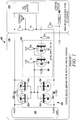
- FIG. 1 illustrates a conventional circuit 100 on a board 120 designed to be selectively AC or DC coupled.
- circuit 100 is coupled to an external sink device 140.
- Circuit 100 includes an integrated circuit chip (IC) 130 and board components 150.
- Board components 150 include two AC coupling capacitors 152 , a transistor switch 154 to short the AC coupling capacitors 152 , and buffering circuitry 156 to drive the gates of transistor switch 154 based on the detection of the type of sink device 140.
- board components 150 are off-chip, and therefore take up a significant amount of surface area on board 120. Further, the use of off-chip components typically increases the overall price of the finished circuit board.
- FIG. 2A illustrates a circuit 200 exemplary of an embodiment of the present invention.
- Circuit 200 is built on a board 220 and is designed to be selectively AC or DC coupled. As illustrated, board 220 may be coupled at coupling points 260 to an external sink device 240.
- Circuit 200 includes an IC 210 mounted on board 220 and board components 250 also formed on board 220.
- Board components 250 include two AC coupling capacitors 252.
- IC 210 includes two AC connectors (AC_P and AC_N) connected to coupling points 260 by way of coupling capacitors 252 for AC coupling, and two DC connectors (DC0 and DC1) connected to coupling points 260 for DC coupling.
- IC 210 also includes a differential driver 212 and two single ended drivers 214.
- the design of differential driver 212 and single ended drivers 214 may for example be based on pending U.S. patent application No. 61/081,515 , entitled “INPUT/OUTPUT BUFFER WITH MULTI-FUNCTION OPERATION AND HIGH VOLTAGE TOLERANCE", filed on July 17, 2008, the subject matter of which is incorporated by reference herein.
- Differential driver 212 and single-ended drivers 214 are turned on or off by control signals upstream. They are typically not turned on at the same time, but may both be turned off at the same time.
- IC 210 also includes two switches 230 interposed between the AC_P/AC_N and DC0/DC1 connectors, respectively. As described in more detail below, switches 230 are configured to short the AC_P/AC_N and DC0/DC1 connectors, thereby shorting AC coupling capacitors 252 , when IC 210 is DC coupled. In other words, IC 210 is capable of selectively shorting AC coupling capacitors 252 depending on the type of coupling (AC or DC) detected.
- this approach brings the switch (and associated circuitry) for shorting the coupling capacitors inside the IC, thus reducing the number of board components required to implement selective AC/DC coupling.
- Detection of coupling mode is done via weak pull-down resistors and Schmitt trigger receivers (not shown) integrated into IC 210.
- IC 210 On power up, IC 210 automatically configures to DC coupling mode and sets a mode status signal (Modeb) to logic high.
- a pad controller (not shown) enables the weak pull down resistors and receivers and monitors the receivers output. When the receivers output is logic high, an external pull up voltage exists, and the pad controller sets Modeb to logic high for DC coupling mode. When the receivers output is logic low, the pad may be either floating or AC coupled.
- the pad controller checks a detect pin (shown in FIG . 2A ) in the AUX connector (not shown) which is received as an input by IC 210.
- the pad is floating and the pad controller maintains the DC coupling mode setting. If the receivers output for the detect pin input is logic low, the pad is AC coupled, and the pad controller sets Modeb to logic low for AC coupling mode.
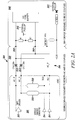
- each switch 230 is implemented as a Metal-Oxide-Semiconductor Field-Effect Transistor (MOSFET) bridge such as MOSFET bridge 232 shown in FIG. 2B .
- MOSFET bridge 232 includes a switch control MOSFET 236 , dynamic bias nMOSFETs 238 , and dynamic bias pMOSFETs 234.
- Switch control MOSFET 236 controls whether MOSFET bridge 232 is on (switch is closed) or off (switch is open).
- nMOSFETs 238 are arranged in series with switch control MOSFET 236 as shown in FIG. 2B . As further described below, nMOSFETs 238 are dynamically biased in order to protect switch control MOSFET 236 from high voltages at the DC0/DC1 connectors required by certain DC coupled interfaces.
- the number of dynamically biased nMOSFETs 238 in each MOSFET bridge 232 depends on the multiplication factor of the external supply tolerance required (as shown in FIG. 2A , external pull-up supply 242 ). Thus, depending on the multiplication factor of external pull-up supply 242 , a number of bias voltages are generated internally by sourcing current from external pull-up 242 through the R1 and DC0/DC1 connectors.
- bias voltages are designed such that the maximum gate-to-source voltage (VGS) of the bridge MOSFETs is not violated.
- the bridge MOSFETs lie in a floating well (not shown) for maximum gate-to-bulk voltage (VGB) not to be violated.
- VGS gate-to-source voltage
- VGB maximum gate-to-bulk voltage
- Each nMOSFET 238 offers a step down voltage at its drain depending on its VGS. By chaining enough dynamically biased nMOSFETs 238 one can achieve multiple step down voltages relative to external pull-up.
- pMOSFETs 234 are arranged in parallel with switch control MOSFET 236 and dynamic bias nMOSFETs 238 ( FIG. 2B ). pMOSFETs 234 , which as further described below are also dynamically biased, address the dynamic range limitations associated with single-channel MOS switches.
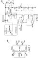
- FIG. 3 illustrates an exemplary MOSFET bridge 332 for use as switch 230.
- MOSFET bridge 332 employs 1X transistors and 1X Vddio power supply voltage (1.8V in the example), and supports 3X external pull up supply (5.0V in the example) in DC coupling mode, where X is a scale factor.
- MOSFET bridge 332 includes a switch control MOSFET 336 , four dynamic bias nMOSFETs 338, and two dynamic bias pMOSFETs 334. Since each 1X MOS transistor can withstand 1X volt between its drain and source, drain and gate, and source and gate, the cascaded arrangement is used to support 3X external pull up supply.
- the Nwell should be floating since the design employs 1X Vddio power supply (1.8V in the example) whereas external pull up 242 may be 3x (5V in the example).
- the Nwell in MOSFET bridge 332 may be shared with single ended drivers 214 in order to save silicon area, as both Nwells have the same behaviour.
- the bias signals NG1 and NG2 are generated from a variable and dynamic bias generation circuit which samples DC0/DC1 voltage, and the signal NG1AC is generated from another variable and dynamic bias generation circuit which samples AC_P/AC_N voltage.
- the result is an open connection at switches 230 between the AC_P/AC_N and DC0/DC1 connectors, respectively.
- AC_P/AC_N voltage In AC coupled mode, AC_P/AC_N voltage is defined by IC 210 itself and the maximum voltage is less than 1.8V.
- DC0/DC1 is connected to the external sink device directly. The maximum allowable voltage at DC0/DC1 is 1.8V+Vthp.
- the minimum allowable voltage at DC0/DC1 is -Vthn.
- Single ended drivers 214 are turned off with high impedance and high voltage tolerance and differential driver 212 is configured to turn on.
- Differential driver 212 is configured to turn off with high impedance and high voltage tolerance (for example DDC mode) and single ended drivers 214 are used to transmit data.
- external pull-up 242 will charge internal dynamic bias circuits which will ramp the voltages at the gates of dynamic bias MOSFETs 334, 338 in MOSFET bridge 332.
- Table 1 Bridge Operation Analysis 1X Power, 1X Transistors & 3X External Pull up Coupling NG1 NG2 Modeb NG1AC Nwell PADDC & PADAC External Pull Up AC 1.8-Vthn (1x) 1.8-Vthn (1x) 0 1.8V (1x) 1.8V (1x) AC output N/A DC 3.6V (2x) 1.8V (1x) 1.8V (1x) 3.6V (2x) 5.0V (3x) 5V (3x) 5V (3x) DC 1.8V (1x) 1.8V (1x) 1.8V (1x) 1.8V (1x) 1.8V (1x) 1.8V (1x) 1.8-Vthn 0 5V (3x)
- FIG. 4 illustrates an exemplary variable and dynamic bias circuit 400 designed to generate the signals NG1 and NG2 of FIG. 3 .
- Transistors M1 and M5 are low threshold devices and other devices are regular ones.
- Transistor M1 is always on and traces the PAD 402 voltage level dynamically.
- Transistor M8 is diode connected and always on if IC 210 power Vddio exists.
- the dynamic bias circuit 400 may encounter two possible scenarios: 1X Vddio is off and 3X external pull up is on, or both 1X Vddio and 3X external pull up are on.
- 1X Vddio (1.8V in this example) is off and 3X external pull up power (5.0V in this example) is applied at PAD 402, diode connected transistors M2, M4 and M7 are on and transistors M3 and M5 are off.
- Vddiob is high, therefore transistor M6 is on and transistor M0 is off.
- Bias signals NG1 and NG2 are thus generated from what is effectively a voltage divider and are equal to about 3.6V and 1.8V, respectively.
- the circuit will draw about 20-30u current from the 3X external pull up and the voltage drop across external pull up resistor 404 (1k-10k resistor in this example) is 200mv at most.
- the voltage drop across the pull up resistor 404 is about 4% of the 3X pull up power and can be neglected.
- the differential driver 212 and single ended drivers 214 are also implemented with 1X voltage tolerant devices, 1X power supply voltage, and support for 3X external pull up voltage.
- Differential driver 212 supports both AC interface standards, such as DisplayPort Auxiliary (DP AUX), and DC interface standards, such as open drain interface or Display Data Channel (DDC).
- DP AUX terminates with 50ohm impedance at both source and destination sides as required by the DisplayPort standard. External device detection is performed at power up or plug/unplug connection to determine what kind of panels, for example, DP or HDMI/DVI, are connected and to configure differential driver 212 to the correct mode.
- Single ended drivers 214 only support DC interface standards, such as open drain interface or Display Data Channel (DDC).
- the external pull up voltage of DDC interface can be up to 3X higher than the IC 1X power supply voltage and the maximum allowable 1X device voltage.
- both 1X and 2X bias voltages have to be generated internally from the 3X external pull up voltage to protect the 1X voltage tolerant devices.
- the IC 1X power supply voltage is on, only the 2X bias voltage is generated from the 3X external pull up voltage and the 1X bias voltage is derived from the IC 1X power supply voltage.
- the N-well of the IC PMOS output buffer should be floating since the 3X external pull voltage up is greater than the IC 1X power supply voltage.
- FIG. 5 illustrates an exemplary MOSFET bridge 532 for use as switch 230 with 1X voltage tolerant devices, 1X power supply voltage (2.5V in this example) and support for 2X external pull up voltage (5.0V in this example).
- MOSFET bridge 532 includes a switch control MOSFET 536 , two dynamic bias nMOSFETs 538, and two dynamic bias pMOSFETs 534.
- the bias signal NG1 is generated from a variable and dynamic bias generation circuit which samples DC0/DC1 voltage
- the signal NG1AC is generated from another variable and dynamic bias generation circuit which samples AC_P/AC_N voltage.
- the signal Nwell in MOSFET bridge 532 may be shared with an Nwell signal (not shown) in single ended drivers 214 in order to save silicon area, as both Nwells have the same behaviour.
- the maximum allowable voltage range across DC0 and DC1 is between 2.5V+Vthp and -Vthn, where Vthn and Vthp are MOSFET absolute value threshold voltages.
- Single ended drivers 214 are turned off with high impedance and high voltage tolerance and differential driver 212 is configured to turn on.
- Differential driver 212 is configured to turn off with high impedance and high voltage tolerance (for example DDC mode) and single ended drivers 214 are used to transmit data.
- external pull-up 242 will power internal dynamic bias circuits which will ramp the voltages at the gates of dynamic bias MOSFETs 534, 538 in MOSFET bridge 532 when Vddio is off.
- Vddio will power dynamic bias MOSFETs 534, 538 in MOSFET bridge 532 instead of external pull up power when Vddio is on
- Node voltages of the MOSFET bridge 532 are listed as follow in AC and DC interfaces in Table 2: Table 2: Bridge Operation Analysis 1X Power, 1X Transistors & 2X External Pull up Voltage Coupling NG1 Modeb NG1AC Nwell PADDC & PADAC External Pull Up AC 2.5-Vthn (1x) 0 2.5V (1x) 2.5V (1x) AC output N/A DC 2.5V (1x) 2.5V (1x) 2.5V (1x) 5.0V (2x) 5V (2x) 5V (2x) DC 2.5V (1x) 2.5V (1x) 2.5V (1x) 2.5-Vthn 0 5V (2x)
- FIG. 6 illustrates a variable and dynamic bias circuit 600 designed to generate the signal NG1 of FIG. 5 . Since in this example MOSFET bridge 532 is only required to tolerate 2X external pull up voltage instead of 3X voltage, the scheme shown in FIG. 4 can be simplified. Specifically, the scheme shown in FIG. 6 only generates one bias voltage (1X volts) and does not consume DC current when Vddio is on and Modeb is high(2.5V in the example).
- Transistors M3, M4, M5 and M6 form another voltage divider and provide bias for transistor M12.
- Transistors M2 and M1 consist of a bypass circuit at start up to start the circuit. When 1X Vddio (2.5V in the example) is off and 2X external pull up (5V in the example) power is on, the circuit draws about 15-30u current from external pull up and the voltage drop across external pull up resistor 604 is 200mv at most.
- PAD 602 voltage is about 4.8V.
- Transistors M3, M4, M6, M8, M9, M10, M11 and M12 are on, and transistors M1 and M2 transition from on to off at external pull up power start up since the voltage drop across M12 is dominant over one over M2 and M1 and is less than 2Vthp absolute value.
- Vddiob is high and equal to the NG1 voltage level, therefore, transistors M5 and M7 are on and transistor M0 is off.
- the NG1 voltage as derived from the voltage divider is about 2.5V.
- Vddiob When both 1X Vddio and 2X external pull up power are on, Vddiob is 0 and transistors M5 and M7 are off, therefore, the two voltage dividers are off and no current is drawn from the 2X external pull up.
- Transistor M0 is on and NG1 is shorted with Vddio. In other words, NG1 is 2.5V regardless of PAD 602 status.
- the signal Charge is asserted by resistor R0 so that transistors M3, M4 and M12 can avoid potential overstress voltage, limiting voltage across their gate-junctions or junctions-junctions to be 1X voltage.
- signal Modeb is 0 and vddiob is high and equal to 2.5V in this case.
- transistors M5 and M7 are on and transistor M0 is off.
- NG1 is 1.8-Vthn since transistor M13 is diode connected and always on.
- the maximum allowable voltage range across DC0 and DC1 is between 2.5V+Vthp and -Vthn for AC coupling mode, and PAD 602 voltage cannot impact NG1 voltage.
- Transistor M11 is off, thus NG1 voltage cannot impact PAD 602 voltage.
- Transistors M7, M8, M9 are on and consume current in the range of 10-30u from Vddio.
- Transistors M3, M4, M5, M6 are on and may consume currents in the range of 5-30u from PAD 602 if PAD 602 voltage is greater than 2*Vthp absolute value.
- the differential driver 212 and single ended drivers 214 are also implemented with 1X voltage tolerant devices, 1X power supply voltage, and support for 2X external pull up voltage.
- Differential driver 212 supports both AC interface standards, such as DisplayPort Auxiliary (DP AUX), and DC interface standards, such as open drain interface or Display Data Channel (DDC).
- DP AUX terminates with 50ohm impedance at both source and destination sides as required by the DisplayPort standard. External device detection is performed at power up or plug/unplug connection to determine what kind of panels, for example, DP or DVI/HDMI, are connected and to configure differential driver 212 to the correct mode.
- Single ended drivers 214 only support DC interface standards, such as open drain interface or Display Data Channel (DDC).
- the external pull up voltage of the DDC interface can be up to 2X higher than the IC 1X power supply voltage and the maximum allowable 1X device voltage.
- 1X bias voltage has to be generated internally from the 2X external pull up voltage to protect the 1X voltage tolerant devices.
- the IC 1X power supply voltage is on, 1X bias voltage is derived from the IC 1X power supply voltage.
- the N-well of the IC PMOS output buffer should be floating since the 2X external pull up voltage is greater than the IC 1X power supply voltage.
- IC 210 may be formed using conventional application specific integrated circuit (ASIC) design and manufacturing techniques.
- IC 210 may for example be formed from Hardware Description Language (HDL) code that describes IC 210 and its various circuits, exemplary of embodiments of the present invention.
- HDL code may be stored on a computer readable medium.
Landscapes
- Engineering & Computer Science (AREA)
- Power Engineering (AREA)
- Computer Hardware Design (AREA)
- Physics & Mathematics (AREA)
- Computing Systems (AREA)
- General Engineering & Computer Science (AREA)
- Mathematical Physics (AREA)
- Semiconductor Integrated Circuits (AREA)
- Electronic Switches (AREA)
Claims (13)
- Chip eines integrierten Schaltkreises (integrated circuit - IC), der angepasst ist, um zur Signalisierung an eine externe Vorrichtung (240) selektiv wechselstrom- oder gleichstromgekoppelt zu werden, wobei der IC-Chip Folgendes umfasst:einen ersten Differentialtreiber (212), der für Wechselstrom- und Gleichstromsignalisierung konfigurierbar ist;eine Vielzahl von ersten Anschlüssen (AC_P, AC_N), die mit dem ersten Differentialtreiber (212) verbunden ist, wobei die Vielzahl von ersten Anschlüssen (AC_P, AC_N), die sich an dem IC-Chip befindet, mit Kopplungspunkten (260) außerhalb des IC-Chips durch entsprechende Kopplungskondensatoren (252) außerhalb des IC-Chips verbindbar ist, um den IC-Chip an die externe Vorrichtung (240) wechselstromzukoppeln;eine zweite einzelendige Treiberkonfiguration (214) zur Gleichstromsignalisierung;eine Vielzahl von zweiten Anschlüssen (DCO, DC1), die mit der zweiten einzelendigen Treiberkonfiguration (214) verbunden ist, wobei die Vielzahl von zweiten Anschlüssen (DCO, DC1), die sich an dem IC-Chip befindet, mit den Kopplungspunkten (260) außerhalb des IC-Chips verbindbar ist, um den IC-Chip an die externe Vorrichtung (240) gleichstromzukoppeln; undSchaltlogik (230), die an dem IC-Chip integriert ist, um die Vielzahl von ersten Anschlüssen (AC_P, AC_N) und die Vielzahl von zweiten Anschlüssen (DCO, DC1) des IC-Chips durch den IC-Chip selektiv miteinander zu verbinden, wodurch jeder der entsprechenden Kopplungskondensatoren (252) kurzgeschlossen wird, wenn der IC-Chip durch die Vielzahl von zweiten Anschlüssen (DCO, DC1) an die Vorrichtung (240) gleichstromgekoppelt ist.
- Integrierter Schaltkreis nach Anspruch 1, wobei die Schaltlogik (230) einen MOSFET-Typ-Schalter umfasst.
- Integrierter Schaltkreis nach Anspruch 1, wobei die Schaltlogik (230) eine MOSFET-Brücke umfasst, wobei die MOSFET-Brücke ferner eine Vielzahl von nMOSFETs, die in Reihe mit einem Schaltsteuer-MOSFET verbunden ist, und eine Vielzahl von pMOSFETs umfasst, die parallel mit dem Schaltsteuer-MOSFET und der Vielzahl von nMOSFETs verbunden ist, wobei die Vielzahl von nMOSFETs eine Vielzahl von Step-Down-Spannungen relativ zu einer externen Zufuhrspannung bereitstellt.
- Integrierter Schaltkreis nach Anspruch 3, wobei die MOSFET-Brücker ferner Folgendes umfasst:
den Schaltsteuer-MOSFET, der zwischen dem ersten und dem zweiten Anschluss verbunden ist, wobei der Schaltsteuer-MOSFET an seinem Gate ein Modusstatussignal empfängt, um den Schaltsteuer-MOSFET einzuschalten und dadurch die MOSFET-Brücke kurzzuschließen, wenn der integrierte Schaltkreis an die Vorrichtung gleichstromgekoppelt ist. - Integrierter Schaltkreis nach Anspruch 4, wobei die Anzahl an nMOSFETs in der MOSFET-Brücke ausgewählt ist, um einen Multiplikationsfaktor einer externen Zufuhrspannung zu tolerieren.
- Integrierter Schaltkreis nach Anspruch 4, wobei die MOSFET-Brücke ferner einen dynamischen Vorspannungsschaltkreis umfasst, um Spannungen an den Gates der nMOSFETs bereitzustellen.
- Integrierter Schaltkreis nach Anspruch 6, wobei die MOSFET-Brücke ferner einen dynamischen Vorspannungsschaltkreis umfasst, um Spannungen an den Gates sowohl der nMOSFETs als auch der pMOSFETs bereitzustellen.
- Verfahren zur selektiven Wechselstrom- oder Gleichstromkopplung eines Chips eines integrierten Schaltkreises (IC) zur Signalisierung an eine externe Vorrichtung (240) an Kopplungspunkten (260) außerhalb des IC-Chips, wobei der IC-Chip einen ersten Differentialtreiber (212), der für Wechselstrom- und Gleichstromsignalisierung konfigurierbar ist; eine Vielzahl von ersten Anschlüssen (AC_P, AC_N), die mit dem ersten Differentialtreiber (212) verbunden ist, wobei die Vielzahl von ersten Anschlüssen (AC_P, AC_N) mit den Kopplungspunkten (260) durch entsprechende Kopplungskondensatoren (252) außerhalb des IC-Chips zur Wechselstromkopplung verbindbar ist; eine zweite einzelendige Treiberkonfiguration (214) zur Gleichstromsignalisierung; und eine Vielzahl von zweiten Anschlüssen (DCO, DC1), die mit der zweiten einzelendigen Treiberkonfiguration (214) verbunden ist, umfasst, wobei die Vielzahl von zweiten Anschlüssen (DCO, DC1) mit den Kopplungspunkten (260) zur Gleichstromkopplung verbindbar ist,
wobei das Verfahren Folgendes umfasst:
Schließen von Schaltlogik (230), die innerhalb des IC-Chips gebildet ist, um die Vielzahl von ersten Anschlüssen (AC_P, AC_N) und die Vielzahl von zweiten Anschlüssen (DCO, DC1) durch den IC-Chip selektiv zu verbinden, wodurch jeder der entsprechenden Kopplungskondensatoren (252) kurzgeschlossen wird, wenn der IC-Chip an die Vorrichtung (240) gleichstromgekoppelt ist. - Verfahren nach Anspruch 8, wobei die Schaltlogik (230) einen MOSFET-Typ-Schalter in dem integrierten Schaltkreis umfasst.
- Verfahren nach Anspruch 8, wobei die Schaltlogik (230) ferner eine MOSFET-Brücke umfasst, wobei die MOSFET-Brücke ferner eine Vielzahl von nMOSFETs, die in Reihe mit einem Schaltsteuer-MOSFET verbunden ist, und eine Vielzahl von pMOSFETs umfasst, die parallel mit dem Schaltsteuer-MOSFET und der Vielzahl von nMOSFETs verbunden ist, wobei die Vielzahl von nMOSFETs eine Vielzahl von Step-Down-Spannungen relativ zu einer externen Zufuhrspannung bereitstellt.
- Verfahren nach Anspruch 10, wobei die MOSFET-Brücke den Schaltsteuer-MOSFET umfasst, der zwischen dem ersten und dem zweiten Anschluss verbunden ist, wobei das Verfahren ferner das Empfangen eines Modusstatussignals an einem Gate des Schaltsteuer-MOSFETs umfasst, um den Schaltsteuer-MOSFET einzuschalten und dadurch die MOSFET-Brücke selektiv kurzzuschließen, wenn der integrierte Schaltkreis an die Vorrichtung gleichstromgekoppelt ist.
- Verfahren nach Anspruch 10, wobei die MOSFET-Brücke ferner einen dynamischen Vorspannungsschaltkreis umfasst, um Spannungen an den Gates der Vielzahl von nMOSFETs bereitzustellen.
- Verfahren nach Anspruch 10, wobei die MOSFET-Brücke ferner einen dynamischen Vorspannungsschaltkreis umfasst, um Spannungen an den Gates sowohl der nMOSFETs als auch der pMOSFETs bereitzustellen.
Applications Claiming Priority (2)
| Application Number | Priority Date | Filing Date | Title |
|---|---|---|---|
| US12/562,703 US8188615B2 (en) | 2009-09-18 | 2009-09-18 | Integrated circuit adapted to be selectively AC or DC coupled |
| PCT/CA2010/001427 WO2011032267A1 (en) | 2009-09-18 | 2010-09-14 | An integrated circuit adapted to be selectively ac or dc coupled |
Publications (3)
| Publication Number | Publication Date |
|---|---|
| EP2478627A1 EP2478627A1 (de) | 2012-07-25 |
| EP2478627A4 EP2478627A4 (de) | 2015-06-03 |
| EP2478627B1 true EP2478627B1 (de) | 2020-04-15 |
Family
ID=43756002
Family Applications (1)
| Application Number | Title | Priority Date | Filing Date |
|---|---|---|---|
| EP10816513.5A Active EP2478627B1 (de) | 2009-09-18 | 2010-09-14 | Für selektive wechselstrom- oder gleichstromkopplung angepasster integrierter schaltkreis |
Country Status (6)
| Country | Link |
|---|---|
| US (1) | US8188615B2 (de) |
| EP (1) | EP2478627B1 (de) |
| JP (1) | JP5690341B2 (de) |
| KR (1) | KR101621035B1 (de) |
| CN (1) | CN102484417B (de) |
| WO (1) | WO2011032267A1 (de) |
Families Citing this family (12)
| Publication number | Priority date | Publication date | Assignee | Title |
|---|---|---|---|---|
| US9234930B2 (en) * | 2010-02-10 | 2016-01-12 | Lattice Semiconductor Corporation | Determination of physical connectivity status of devices based on electrical measurement |
| US8867216B2 (en) | 2011-04-05 | 2014-10-21 | Advanced Micro Devices, Inc. | Slot design for flexible and expandable system architecture |
| EP2696490B1 (de) * | 2012-08-09 | 2018-01-10 | Nxp B.V. | AC/DC-Wandler-Schaltung |
| US9454503B1 (en) | 2013-08-09 | 2016-09-27 | Google Inc. | Hot swap decoupling for noise reduction and failure prevention |
| CN103634124A (zh) * | 2013-11-27 | 2014-03-12 | 苏州贝克微电子有限公司 | 一种可选择的多协议电缆终端 |
| US10050623B2 (en) * | 2015-07-17 | 2018-08-14 | Intel Corporation | High performance repeater |
| US9965370B2 (en) * | 2015-12-24 | 2018-05-08 | Intel Corporation | Automated detection of high performance interconnect coupling |
| JP6538593B2 (ja) * | 2016-03-11 | 2019-07-03 | 東芝メモリ株式会社 | ホスト装置 |
| JP6613369B2 (ja) * | 2016-04-26 | 2019-11-27 | マクセル株式会社 | 映像出力システム、映像出力装置、および接続ケーブル |
| CN107766278B (zh) * | 2017-11-08 | 2020-06-05 | 清华大学 | 一种兼容直流/交流耦合的高速串行接口接收机前端电路 |
| US11019392B2 (en) | 2019-07-19 | 2021-05-25 | Semiconductor Components Industries, Llc | Methods and apparatus for an output buffer |
| GB201915873D0 (en) * | 2019-10-31 | 2019-12-18 | B Secur Ltd | Device, system and method for acquiring and monitoring of biometric electrical signals |
Family Cites Families (17)
| Publication number | Priority date | Publication date | Assignee | Title |
|---|---|---|---|---|
| US5596297A (en) * | 1994-12-20 | 1997-01-21 | Sgs-Thomson Microelectronics, Inc. | Output driver circuitry with limited output high voltage |
| US6822470B2 (en) * | 1995-08-30 | 2004-11-23 | Micron Technology, Inc. | On-chip substrate regulator test mode |
| US5864457A (en) * | 1997-01-21 | 1999-01-26 | Dell Usa, L.P. | System and method for controlling current flow in an AC adapter |
| KR100259841B1 (ko) * | 1997-07-31 | 2000-06-15 | 윤종용 | 씽글 칩을 이용한 피씨아이 버스의 핫 플러그 제어기 |
| JP2001144555A (ja) * | 1999-11-11 | 2001-05-25 | Keyence Corp | 信号入力回路および波形観察装置 |
| US6574695B1 (en) * | 2000-01-06 | 2003-06-03 | Sun Microsystems, Inc. | System and method for providing hot swap capability using existing circuits and drivers with minimal changes |
| US6886057B2 (en) | 2002-06-06 | 2005-04-26 | Dell Products L.P. | Method and system for supporting multiple bus protocols on a set of wirelines |
| US6968413B2 (en) * | 2002-10-07 | 2005-11-22 | International Business Machines Corporation | Method and system for configuring terminators in a serial communication system |
| US7138730B2 (en) * | 2002-11-22 | 2006-11-21 | Virginia Tech Intellectual Properties, Inc. | Topologies for multiple energy sources |
| ATE377282T1 (de) * | 2003-03-10 | 2007-11-15 | Det Int Holding Ltd | Gleichstrom-gleichstrom-schaltwandlereinrichtun |
| US7053657B1 (en) * | 2003-06-26 | 2006-05-30 | Cypress Semiconductor Corporation | Dynamically biased wide swing level shifting circuit for high speed voltage protection input/outputs |
| US7533208B2 (en) * | 2005-09-26 | 2009-05-12 | Silicon Graphics, Inc. | Hot plug control apparatus and method |
| US7439760B2 (en) | 2005-12-19 | 2008-10-21 | Rambus Inc. | Configurable on-die termination |
| US8958575B2 (en) | 2007-06-29 | 2015-02-17 | Qualcomm Incorporated | Amplifier with configurable DC-coupled or AC-coupled output |
| US8129867B2 (en) * | 2008-06-27 | 2012-03-06 | National Instruments Corporation | RF AC/DC coupling circuit using general purpose solid-state relay |
| US8344760B2 (en) * | 2008-07-17 | 2013-01-01 | Ati Technologies Ulc | Input/output buffer circuit |
| US8237422B2 (en) * | 2009-05-09 | 2012-08-07 | Cosmic Circuits Private Limited | Efficient switch cascode architecture for switching devices |
-
2009
- 2009-09-18 US US12/562,703 patent/US8188615B2/en active Active
-
2010
- 2010-09-14 WO PCT/CA2010/001427 patent/WO2011032267A1/en not_active Ceased
- 2010-09-14 KR KR1020127009880A patent/KR101621035B1/ko active Active
- 2010-09-14 JP JP2012529074A patent/JP5690341B2/ja active Active
- 2010-09-14 CN CN201080040717.9A patent/CN102484417B/zh active Active
- 2010-09-14 EP EP10816513.5A patent/EP2478627B1/de active Active
Non-Patent Citations (1)
| Title |
|---|
| None * |
Also Published As
| Publication number | Publication date |
|---|---|
| CN102484417A (zh) | 2012-05-30 |
| JP2013505600A (ja) | 2013-02-14 |
| KR101621035B1 (ko) | 2016-05-13 |
| JP5690341B2 (ja) | 2015-03-25 |
| EP2478627A1 (de) | 2012-07-25 |
| CN102484417B (zh) | 2016-01-20 |
| US8188615B2 (en) | 2012-05-29 |
| EP2478627A4 (de) | 2015-06-03 |
| KR20120100925A (ko) | 2012-09-12 |
| US20110068632A1 (en) | 2011-03-24 |
| WO2011032267A1 (en) | 2011-03-24 |
Similar Documents
| Publication | Publication Date | Title |
|---|---|---|
| EP2478627B1 (de) | Für selektive wechselstrom- oder gleichstromkopplung angepasster integrierter schaltkreis | |
| US9423815B2 (en) | Differential output circuit and semiconductor device | |
| US6323704B1 (en) | Multiple voltage compatible I/O buffer | |
| US8385036B2 (en) | System and method for negative voltage protection | |
| US8139330B2 (en) | Semiconductor integrated circuit | |
| US7463068B2 (en) | Apparatus and method for over-voltage, under-voltage and over-current stress protection for transceiver input and output circuitry | |
| US20120049939A1 (en) | Input/output circuit | |
| KR19990067849A (ko) | 허용 전압 출력 버퍼 | |
| KR20140129159A (ko) | 차동 입력/출력 인터페이스들에 대한 서지 보호 | |
| US20200264643A1 (en) | Controller area network (can) transceiver | |
| US9762231B2 (en) | Transistors configured for gate overbiasing and circuits therefrom | |
| US10673436B1 (en) | Failsafe device | |
| EP1585278B1 (de) | Daten-Ausgangstreiber mit verbessertem Überspannungsschutz | |
| US7154309B1 (en) | Dual-mode output driver configured for outputting a signal according to either a selected high voltage/low speed mode or a low voltage/high speed mode | |
| US10637473B2 (en) | High voltage tolerant CMOS driver for low-voltage bi-directional communication buses | |
| US11489519B2 (en) | Analog switch with boost current for fast turn on | |
| US11962307B2 (en) | Output circuit having multi-level output and comparator circuit therof | |
| EP1949530A2 (de) | Hochspannungstoleranter port-treiber | |
| US20050041343A1 (en) | Voltage limiting semiconductor pass gate circuit | |
| US9065441B2 (en) | Voltage scale-down circuit | |
| US20250392308A1 (en) | Systems and methods for adaptive gate voltage generation of pad-connected devices | |
| US20160020761A1 (en) | Transmission circuit with leakage prevention circuit | |
| US6765426B1 (en) | Methods and systems for limiting supply bounce | |
| JP2025113907A (ja) | 半導体集積回路 | |
| CN115694142A (zh) | 用于具有高压保护和阻抗控制的多驱动器架构的装置 |
Legal Events
| Date | Code | Title | Description |
|---|---|---|---|
| PUAI | Public reference made under article 153(3) epc to a published international application that has entered the european phase |
Free format text: ORIGINAL CODE: 0009012 |
|
| 17P | Request for examination filed |
Effective date: 20120224 |
|
| AK | Designated contracting states |
Kind code of ref document: A1 Designated state(s): AL AT BE BG CH CY CZ DE DK EE ES FI FR GB GR HR HU IE IS IT LI LT LU LV MC MK MT NL NO PL PT RO SE SI SK SM TR |
|
| DAX | Request for extension of the european patent (deleted) | ||
| RA4 | Supplementary search report drawn up and despatched (corrected) |
Effective date: 20150507 |
|
| RIC1 | Information provided on ipc code assigned before grant |
Ipc: H03K 17/687 20060101ALI20150429BHEP Ipc: H03K 19/0185 20060101ALI20150429BHEP Ipc: H02M 1/10 20060101AFI20150429BHEP |
|
| STAA | Information on the status of an ep patent application or granted ep patent |
Free format text: STATUS: EXAMINATION IS IN PROGRESS |
|
| 17Q | First examination report despatched |
Effective date: 20170220 |
|
| GRAP | Despatch of communication of intention to grant a patent |
Free format text: ORIGINAL CODE: EPIDOSNIGR1 |
|
| STAA | Information on the status of an ep patent application or granted ep patent |
Free format text: STATUS: GRANT OF PATENT IS INTENDED |
|
| INTG | Intention to grant announced |
Effective date: 20191210 |
|
| GRAS | Grant fee paid |
Free format text: ORIGINAL CODE: EPIDOSNIGR3 |
|
| GRAA | (expected) grant |
Free format text: ORIGINAL CODE: 0009210 |
|
| STAA | Information on the status of an ep patent application or granted ep patent |
Free format text: STATUS: THE PATENT HAS BEEN GRANTED |
|
| AK | Designated contracting states |
Kind code of ref document: B1 Designated state(s): AL AT BE BG CH CY CZ DE DK EE ES FI FR GB GR HR HU IE IS IT LI LT LU LV MC MK MT NL NO PL PT RO SE SI SK SM TR |
|
| REG | Reference to a national code |
Ref country code: CH Ref legal event code: EP Ref country code: GB Ref legal event code: FG4D |
|
| REG | Reference to a national code |
Ref country code: DE Ref legal event code: R096 Ref document number: 602010063944 Country of ref document: DE |
|
| REG | Reference to a national code |
Ref country code: IE Ref legal event code: FG4D |
|
| REG | Reference to a national code |
Ref country code: AT Ref legal event code: REF Ref document number: 1258461 Country of ref document: AT Kind code of ref document: T Effective date: 20200515 |
|
| REG | Reference to a national code |
Ref country code: NL Ref legal event code: MP Effective date: 20200415 |
|
| REG | Reference to a national code |
Ref country code: LT Ref legal event code: MG4D |
|
| PG25 | Lapsed in a contracting state [announced via postgrant information from national office to epo] |
Ref country code: LT Free format text: LAPSE BECAUSE OF FAILURE TO SUBMIT A TRANSLATION OF THE DESCRIPTION OR TO PAY THE FEE WITHIN THE PRESCRIBED TIME-LIMIT Effective date: 20200415 Ref country code: PT Free format text: LAPSE BECAUSE OF FAILURE TO SUBMIT A TRANSLATION OF THE DESCRIPTION OR TO PAY THE FEE WITHIN THE PRESCRIBED TIME-LIMIT Effective date: 20200817 Ref country code: NL Free format text: LAPSE BECAUSE OF FAILURE TO SUBMIT A TRANSLATION OF THE DESCRIPTION OR TO PAY THE FEE WITHIN THE PRESCRIBED TIME-LIMIT Effective date: 20200415 Ref country code: FI Free format text: LAPSE BECAUSE OF FAILURE TO SUBMIT A TRANSLATION OF THE DESCRIPTION OR TO PAY THE FEE WITHIN THE PRESCRIBED TIME-LIMIT Effective date: 20200415 Ref country code: SE Free format text: LAPSE BECAUSE OF FAILURE TO SUBMIT A TRANSLATION OF THE DESCRIPTION OR TO PAY THE FEE WITHIN THE PRESCRIBED TIME-LIMIT Effective date: 20200415 Ref country code: IS Free format text: LAPSE BECAUSE OF FAILURE TO SUBMIT A TRANSLATION OF THE DESCRIPTION OR TO PAY THE FEE WITHIN THE PRESCRIBED TIME-LIMIT Effective date: 20200815 Ref country code: NO Free format text: LAPSE BECAUSE OF FAILURE TO SUBMIT A TRANSLATION OF THE DESCRIPTION OR TO PAY THE FEE WITHIN THE PRESCRIBED TIME-LIMIT Effective date: 20200715 Ref country code: GR Free format text: LAPSE BECAUSE OF FAILURE TO SUBMIT A TRANSLATION OF THE DESCRIPTION OR TO PAY THE FEE WITHIN THE PRESCRIBED TIME-LIMIT Effective date: 20200716 |
|
| REG | Reference to a national code |
Ref country code: AT Ref legal event code: MK05 Ref document number: 1258461 Country of ref document: AT Kind code of ref document: T Effective date: 20200415 |
|
| PG25 | Lapsed in a contracting state [announced via postgrant information from national office to epo] |
Ref country code: BG Free format text: LAPSE BECAUSE OF FAILURE TO SUBMIT A TRANSLATION OF THE DESCRIPTION OR TO PAY THE FEE WITHIN THE PRESCRIBED TIME-LIMIT Effective date: 20200715 Ref country code: LV Free format text: LAPSE BECAUSE OF FAILURE TO SUBMIT A TRANSLATION OF THE DESCRIPTION OR TO PAY THE FEE WITHIN THE PRESCRIBED TIME-LIMIT Effective date: 20200415 Ref country code: HR Free format text: LAPSE BECAUSE OF FAILURE TO SUBMIT A TRANSLATION OF THE DESCRIPTION OR TO PAY THE FEE WITHIN THE PRESCRIBED TIME-LIMIT Effective date: 20200415 |
|
| PG25 | Lapsed in a contracting state [announced via postgrant information from national office to epo] |
Ref country code: AL Free format text: LAPSE BECAUSE OF FAILURE TO SUBMIT A TRANSLATION OF THE DESCRIPTION OR TO PAY THE FEE WITHIN THE PRESCRIBED TIME-LIMIT Effective date: 20200415 |
|
| REG | Reference to a national code |
Ref country code: DE Ref legal event code: R097 Ref document number: 602010063944 Country of ref document: DE |
|
| PG25 | Lapsed in a contracting state [announced via postgrant information from national office to epo] |
Ref country code: EE Free format text: LAPSE BECAUSE OF FAILURE TO SUBMIT A TRANSLATION OF THE DESCRIPTION OR TO PAY THE FEE WITHIN THE PRESCRIBED TIME-LIMIT Effective date: 20200415 Ref country code: SM Free format text: LAPSE BECAUSE OF FAILURE TO SUBMIT A TRANSLATION OF THE DESCRIPTION OR TO PAY THE FEE WITHIN THE PRESCRIBED TIME-LIMIT Effective date: 20200415 Ref country code: DK Free format text: LAPSE BECAUSE OF FAILURE TO SUBMIT A TRANSLATION OF THE DESCRIPTION OR TO PAY THE FEE WITHIN THE PRESCRIBED TIME-LIMIT Effective date: 20200415 Ref country code: IT Free format text: LAPSE BECAUSE OF FAILURE TO SUBMIT A TRANSLATION OF THE DESCRIPTION OR TO PAY THE FEE WITHIN THE PRESCRIBED TIME-LIMIT Effective date: 20200415 Ref country code: RO Free format text: LAPSE BECAUSE OF FAILURE TO SUBMIT A TRANSLATION OF THE DESCRIPTION OR TO PAY THE FEE WITHIN THE PRESCRIBED TIME-LIMIT Effective date: 20200415 Ref country code: AT Free format text: LAPSE BECAUSE OF FAILURE TO SUBMIT A TRANSLATION OF THE DESCRIPTION OR TO PAY THE FEE WITHIN THE PRESCRIBED TIME-LIMIT Effective date: 20200415 Ref country code: CZ Free format text: LAPSE BECAUSE OF FAILURE TO SUBMIT A TRANSLATION OF THE DESCRIPTION OR TO PAY THE FEE WITHIN THE PRESCRIBED TIME-LIMIT Effective date: 20200415 Ref country code: ES Free format text: LAPSE BECAUSE OF FAILURE TO SUBMIT A TRANSLATION OF THE DESCRIPTION OR TO PAY THE FEE WITHIN THE PRESCRIBED TIME-LIMIT Effective date: 20200415 |
|
| PLBE | No opposition filed within time limit |
Free format text: ORIGINAL CODE: 0009261 |
|
| STAA | Information on the status of an ep patent application or granted ep patent |
Free format text: STATUS: NO OPPOSITION FILED WITHIN TIME LIMIT |
|
| PG25 | Lapsed in a contracting state [announced via postgrant information from national office to epo] |
Ref country code: PL Free format text: LAPSE BECAUSE OF FAILURE TO SUBMIT A TRANSLATION OF THE DESCRIPTION OR TO PAY THE FEE WITHIN THE PRESCRIBED TIME-LIMIT Effective date: 20200415 Ref country code: SK Free format text: LAPSE BECAUSE OF FAILURE TO SUBMIT A TRANSLATION OF THE DESCRIPTION OR TO PAY THE FEE WITHIN THE PRESCRIBED TIME-LIMIT Effective date: 20200415 |
|
| 26N | No opposition filed |
Effective date: 20210118 |
|
| PG25 | Lapsed in a contracting state [announced via postgrant information from national office to epo] |
Ref country code: MC Free format text: LAPSE BECAUSE OF FAILURE TO SUBMIT A TRANSLATION OF THE DESCRIPTION OR TO PAY THE FEE WITHIN THE PRESCRIBED TIME-LIMIT Effective date: 20200415 |
|
| REG | Reference to a national code |
Ref country code: CH Ref legal event code: PL |
|
| PG25 | Lapsed in a contracting state [announced via postgrant information from national office to epo] |
Ref country code: SI Free format text: LAPSE BECAUSE OF FAILURE TO SUBMIT A TRANSLATION OF THE DESCRIPTION OR TO PAY THE FEE WITHIN THE PRESCRIBED TIME-LIMIT Effective date: 20200415 |
|
| REG | Reference to a national code |
Ref country code: BE Ref legal event code: MM Effective date: 20200930 |
|
| PG25 | Lapsed in a contracting state [announced via postgrant information from national office to epo] |
Ref country code: LU Free format text: LAPSE BECAUSE OF NON-PAYMENT OF DUE FEES Effective date: 20200914 |
|
| PG25 | Lapsed in a contracting state [announced via postgrant information from national office to epo] |
Ref country code: FR Free format text: LAPSE BECAUSE OF NON-PAYMENT OF DUE FEES Effective date: 20200930 |
|
| PG25 | Lapsed in a contracting state [announced via postgrant information from national office to epo] |
Ref country code: BE Free format text: LAPSE BECAUSE OF NON-PAYMENT OF DUE FEES Effective date: 20200930 Ref country code: CH Free format text: LAPSE BECAUSE OF NON-PAYMENT OF DUE FEES Effective date: 20200930 Ref country code: LI Free format text: LAPSE BECAUSE OF NON-PAYMENT OF DUE FEES Effective date: 20200930 Ref country code: IE Free format text: LAPSE BECAUSE OF NON-PAYMENT OF DUE FEES Effective date: 20200914 |
|
| PG25 | Lapsed in a contracting state [announced via postgrant information from national office to epo] |
Ref country code: TR Free format text: LAPSE BECAUSE OF FAILURE TO SUBMIT A TRANSLATION OF THE DESCRIPTION OR TO PAY THE FEE WITHIN THE PRESCRIBED TIME-LIMIT Effective date: 20200415 Ref country code: MT Free format text: LAPSE BECAUSE OF FAILURE TO SUBMIT A TRANSLATION OF THE DESCRIPTION OR TO PAY THE FEE WITHIN THE PRESCRIBED TIME-LIMIT Effective date: 20200415 Ref country code: CY Free format text: LAPSE BECAUSE OF FAILURE TO SUBMIT A TRANSLATION OF THE DESCRIPTION OR TO PAY THE FEE WITHIN THE PRESCRIBED TIME-LIMIT Effective date: 20200415 |
|
| PG25 | Lapsed in a contracting state [announced via postgrant information from national office to epo] |
Ref country code: MK Free format text: LAPSE BECAUSE OF FAILURE TO SUBMIT A TRANSLATION OF THE DESCRIPTION OR TO PAY THE FEE WITHIN THE PRESCRIBED TIME-LIMIT Effective date: 20200415 |
|
| P01 | Opt-out of the competence of the unified patent court (upc) registered |
Effective date: 20230530 |
|
| PGFP | Annual fee paid to national office [announced via postgrant information from national office to epo] |
Ref country code: DE Payment date: 20250819 Year of fee payment: 16 |
|
| PGFP | Annual fee paid to national office [announced via postgrant information from national office to epo] |
Ref country code: GB Payment date: 20250911 Year of fee payment: 16 |