EP2472573A1 - Verfahren zur Herstellung eines vertikalen Transistors und vertikaler Transistor - Google Patents
Verfahren zur Herstellung eines vertikalen Transistors und vertikaler Transistor Download PDFInfo
- Publication number
- EP2472573A1 EP2472573A1 EP11150120A EP11150120A EP2472573A1 EP 2472573 A1 EP2472573 A1 EP 2472573A1 EP 11150120 A EP11150120 A EP 11150120A EP 11150120 A EP11150120 A EP 11150120A EP 2472573 A1 EP2472573 A1 EP 2472573A1
- Authority
- EP
- European Patent Office
- Prior art keywords
- trench
- gate
- electrode
- gate dielectric
- dielectric
- Prior art date
- Legal status (The legal status is an assumption and is not a legal conclusion. Google has not performed a legal analysis and makes no representation as to the accuracy of the status listed.)
- Withdrawn
Links
- 238000004519 manufacturing process Methods 0.000 title claims abstract description 9
- 239000000758 substrate Substances 0.000 claims abstract description 34
- 238000000034 method Methods 0.000 claims abstract description 18
- 239000007772 electrode material Substances 0.000 claims abstract description 17
- 150000004767 nitrides Chemical class 0.000 claims description 19
- 229910021420 polycrystalline silicon Inorganic materials 0.000 claims description 16
- 229920005591 polysilicon Polymers 0.000 claims description 14
- 239000000463 material Substances 0.000 claims description 12
- 230000015572 biosynthetic process Effects 0.000 claims description 11
- 239000004065 semiconductor Substances 0.000 claims description 7
- 238000000151 deposition Methods 0.000 claims description 6
- 238000004518 low pressure chemical vapour deposition Methods 0.000 claims description 3
- 230000008719 thickening Effects 0.000 claims description 3
- 239000012535 impurity Substances 0.000 description 10
- 230000015556 catabolic process Effects 0.000 description 7
- 238000005530 etching Methods 0.000 description 7
- 229910021421 monocrystalline silicon Inorganic materials 0.000 description 7
- VYPSYNLAJGMNEJ-UHFFFAOYSA-N Silicium dioxide Chemical compound O=[Si]=O VYPSYNLAJGMNEJ-UHFFFAOYSA-N 0.000 description 6
- 238000009413 insulation Methods 0.000 description 6
- 229910052581 Si3N4 Inorganic materials 0.000 description 4
- BOTDANWDWHJENH-UHFFFAOYSA-N Tetraethyl orthosilicate Chemical compound CCO[Si](OCC)(OCC)OCC BOTDANWDWHJENH-UHFFFAOYSA-N 0.000 description 4
- 230000008021 deposition Effects 0.000 description 4
- HQVNEWCFYHHQES-UHFFFAOYSA-N silicon nitride Chemical compound N12[Si]34N5[Si]62N3[Si]51N64 HQVNEWCFYHHQES-UHFFFAOYSA-N 0.000 description 4
- 229910052681 coesite Inorganic materials 0.000 description 3
- 229910052906 cristobalite Inorganic materials 0.000 description 3
- 238000005498 polishing Methods 0.000 description 3
- 239000000377 silicon dioxide Substances 0.000 description 3
- 229910052682 stishovite Inorganic materials 0.000 description 3
- 229910052905 tridymite Inorganic materials 0.000 description 3
- XUIMIQQOPSSXEZ-UHFFFAOYSA-N Silicon Chemical compound [Si] XUIMIQQOPSSXEZ-UHFFFAOYSA-N 0.000 description 2
- 229910021417 amorphous silicon Inorganic materials 0.000 description 2
- 230000008901 benefit Effects 0.000 description 2
- 229910052710 silicon Inorganic materials 0.000 description 2
- 239000010703 silicon Substances 0.000 description 2
- 210000000746 body region Anatomy 0.000 description 1
- 230000007547 defect Effects 0.000 description 1
- 230000001419 dependent effect Effects 0.000 description 1
- 230000006866 deterioration Effects 0.000 description 1
- 230000009977 dual effect Effects 0.000 description 1
- 230000005684 electric field Effects 0.000 description 1
- 230000006872 improvement Effects 0.000 description 1
- 239000012212 insulator Substances 0.000 description 1
- 229910044991 metal oxide Inorganic materials 0.000 description 1
- 150000004706 metal oxides Chemical class 0.000 description 1
- 238000001465 metallisation Methods 0.000 description 1
- 238000004806 packaging method and process Methods 0.000 description 1
- 238000007517 polishing process Methods 0.000 description 1
- 239000013641 positive control Substances 0.000 description 1
- 230000008569 process Effects 0.000 description 1
- 230000008439 repair process Effects 0.000 description 1
- 238000001878 scanning electron micrograph Methods 0.000 description 1
- 239000002210 silicon-based material Substances 0.000 description 1
- 239000000126 substance Substances 0.000 description 1
Images


Classifications
-
- H—ELECTRICITY
- H01—ELECTRIC ELEMENTS
- H01L—SEMICONDUCTOR DEVICES NOT COVERED BY CLASS H10
- H01L29/00—Semiconductor devices specially adapted for rectifying, amplifying, oscillating or switching and having potential barriers; Capacitors or resistors having potential barriers, e.g. a PN-junction depletion layer or carrier concentration layer; Details of semiconductor bodies or of electrodes thereof ; Multistep manufacturing processes therefor
- H01L29/66—Types of semiconductor device ; Multistep manufacturing processes therefor
- H01L29/68—Types of semiconductor device ; Multistep manufacturing processes therefor controllable by only the electric current supplied, or only the electric potential applied, to an electrode which does not carry the current to be rectified, amplified or switched
- H01L29/76—Unipolar devices, e.g. field effect transistors
- H01L29/772—Field effect transistors
- H01L29/78—Field effect transistors with field effect produced by an insulated gate
- H01L29/7801—DMOS transistors, i.e. MISFETs with a channel accommodating body or base region adjoining a drain drift region
- H01L29/7802—Vertical DMOS transistors, i.e. VDMOS transistors
- H01L29/7813—Vertical DMOS transistors, i.e. VDMOS transistors with trench gate electrode, e.g. UMOS transistors
-
- H—ELECTRICITY
- H01—ELECTRIC ELEMENTS
- H01L—SEMICONDUCTOR DEVICES NOT COVERED BY CLASS H10
- H01L29/00—Semiconductor devices specially adapted for rectifying, amplifying, oscillating or switching and having potential barriers; Capacitors or resistors having potential barriers, e.g. a PN-junction depletion layer or carrier concentration layer; Details of semiconductor bodies or of electrodes thereof ; Multistep manufacturing processes therefor
- H01L29/40—Electrodes ; Multistep manufacturing processes therefor
- H01L29/402—Field plates
- H01L29/407—Recessed field plates, e.g. trench field plates, buried field plates
-
- H—ELECTRICITY
- H01—ELECTRIC ELEMENTS
- H01L—SEMICONDUCTOR DEVICES NOT COVERED BY CLASS H10
- H01L29/00—Semiconductor devices specially adapted for rectifying, amplifying, oscillating or switching and having potential barriers; Capacitors or resistors having potential barriers, e.g. a PN-junction depletion layer or carrier concentration layer; Details of semiconductor bodies or of electrodes thereof ; Multistep manufacturing processes therefor
- H01L29/66—Types of semiconductor device ; Multistep manufacturing processes therefor
- H01L29/66007—Multistep manufacturing processes
- H01L29/66075—Multistep manufacturing processes of devices having semiconductor bodies comprising group 14 or group 13/15 materials
- H01L29/66227—Multistep manufacturing processes of devices having semiconductor bodies comprising group 14 or group 13/15 materials the devices being controllable only by the electric current supplied or the electric potential applied, to an electrode which does not carry the current to be rectified, amplified or switched, e.g. three-terminal devices
- H01L29/66409—Unipolar field-effect transistors
- H01L29/66477—Unipolar field-effect transistors with an insulated gate, i.e. MISFET
- H01L29/66674—DMOS transistors, i.e. MISFETs with a channel accommodating body or base region adjoining a drain drift region
- H01L29/66712—Vertical DMOS transistors, i.e. VDMOS transistors
- H01L29/66734—Vertical DMOS transistors, i.e. VDMOS transistors with a step of recessing the gate electrode, e.g. to form a trench gate electrode
-
- H—ELECTRICITY
- H01—ELECTRIC ELEMENTS
- H01L—SEMICONDUCTOR DEVICES NOT COVERED BY CLASS H10
- H01L29/00—Semiconductor devices specially adapted for rectifying, amplifying, oscillating or switching and having potential barriers; Capacitors or resistors having potential barriers, e.g. a PN-junction depletion layer or carrier concentration layer; Details of semiconductor bodies or of electrodes thereof ; Multistep manufacturing processes therefor
- H01L29/40—Electrodes ; Multistep manufacturing processes therefor
- H01L29/41—Electrodes ; Multistep manufacturing processes therefor characterised by their shape, relative sizes or dispositions
- H01L29/423—Electrodes ; Multistep manufacturing processes therefor characterised by their shape, relative sizes or dispositions not carrying the current to be rectified, amplified or switched
- H01L29/42312—Gate electrodes for field effect devices
- H01L29/42316—Gate electrodes for field effect devices for field-effect transistors
- H01L29/4232—Gate electrodes for field effect devices for field-effect transistors with insulated gate
- H01L29/42364—Gate electrodes for field effect devices for field-effect transistors with insulated gate characterised by the insulating layer, e.g. thickness or uniformity
- H01L29/42368—Gate electrodes for field effect devices for field-effect transistors with insulated gate characterised by the insulating layer, e.g. thickness or uniformity the thickness being non-uniform
-
- H—ELECTRICITY
- H01—ELECTRIC ELEMENTS
- H01L—SEMICONDUCTOR DEVICES NOT COVERED BY CLASS H10
- H01L29/00—Semiconductor devices specially adapted for rectifying, amplifying, oscillating or switching and having potential barriers; Capacitors or resistors having potential barriers, e.g. a PN-junction depletion layer or carrier concentration layer; Details of semiconductor bodies or of electrodes thereof ; Multistep manufacturing processes therefor
- H01L29/40—Electrodes ; Multistep manufacturing processes therefor
- H01L29/41—Electrodes ; Multistep manufacturing processes therefor characterised by their shape, relative sizes or dispositions
- H01L29/423—Electrodes ; Multistep manufacturing processes therefor characterised by their shape, relative sizes or dispositions not carrying the current to be rectified, amplified or switched
- H01L29/42312—Gate electrodes for field effect devices
- H01L29/42316—Gate electrodes for field effect devices for field-effect transistors
- H01L29/4232—Gate electrodes for field effect devices for field-effect transistors with insulated gate
- H01L29/42372—Gate electrodes for field effect devices for field-effect transistors with insulated gate characterised by the conducting layer, e.g. the length, the sectional shape or the lay-out
- H01L29/42376—Gate electrodes for field effect devices for field-effect transistors with insulated gate characterised by the conducting layer, e.g. the length, the sectional shape or the lay-out characterised by the length or the sectional shape
-
- H—ELECTRICITY
- H01—ELECTRIC ELEMENTS
- H01L—SEMICONDUCTOR DEVICES NOT COVERED BY CLASS H10
- H01L29/00—Semiconductor devices specially adapted for rectifying, amplifying, oscillating or switching and having potential barriers; Capacitors or resistors having potential barriers, e.g. a PN-junction depletion layer or carrier concentration layer; Details of semiconductor bodies or of electrodes thereof ; Multistep manufacturing processes therefor
- H01L29/40—Electrodes ; Multistep manufacturing processes therefor
- H01L29/43—Electrodes ; Multistep manufacturing processes therefor characterised by the materials of which they are formed
- H01L29/49—Metal-insulator-semiconductor electrodes, e.g. gates of MOSFET
- H01L29/51—Insulating materials associated therewith
- H01L29/511—Insulating materials associated therewith with a compositional variation, e.g. multilayer structures
- H01L29/513—Insulating materials associated therewith with a compositional variation, e.g. multilayer structures the variation being perpendicular to the channel plane
-
- H—ELECTRICITY
- H01—ELECTRIC ELEMENTS
- H01L—SEMICONDUCTOR DEVICES NOT COVERED BY CLASS H10
- H01L29/00—Semiconductor devices specially adapted for rectifying, amplifying, oscillating or switching and having potential barriers; Capacitors or resistors having potential barriers, e.g. a PN-junction depletion layer or carrier concentration layer; Details of semiconductor bodies or of electrodes thereof ; Multistep manufacturing processes therefor
- H01L29/40—Electrodes ; Multistep manufacturing processes therefor
- H01L29/43—Electrodes ; Multistep manufacturing processes therefor characterised by the materials of which they are formed
- H01L29/49—Metal-insulator-semiconductor electrodes, e.g. gates of MOSFET
- H01L29/51—Insulating materials associated therewith
- H01L29/518—Insulating materials associated therewith the insulating material containing nitrogen, e.g. nitride, oxynitride, nitrogen-doped material
Definitions
- the present invention relates to a vertical transistor comprising a substrate including a vertical stack of regions including a source region separated from a drain region by a channel region and a trench lined with a gate dielectric liner, said trench at least partially extending through said vertical stack of regions, wherein said trench comprises a shield electrode and a gate electrode surrounding an upper portion of the shield electrode.
- the present invention further relates to a method of manufacturing such a vertical transistor.
- Vertical transistors e.g. trench-MOS (metal oxide semiconductor) transistors are promising devices to allow for the further increase of the device density in a semiconductor chip.
- architectures have been proposed in which in addition to the vertical gate electrode, a shield electrode is provided, as the presence of the shield electrode is known to relax the design choices that govern the tradeoff between the punch-through voltage (BV dss ) and the drain-source on-resistance (R ds-on ) of the transistor.
- BV dss punch-through voltage
- R ds-on drain-source on-resistance
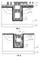
- FIG. 1 provides a sectional view of a vertical MOS transistor comprises an n + -type monocrystalline silicon substrate 1, a drain region 3 made of n - -type impurity semiconductor grown epitaxially on the substrate 1, a channel region 5 made of p-type impurity semiconductor in the drain region 3, a source region 7 made of n + -type impurity semiconductor on the channel region 5, a trench 23 formed through the regions 5 and 7, a shield electrode 11 disposed in the trench 23 to extend above the source region 7 with a relatively thick first gate insulation film 9 interposing between the walls of the trench 23 and the shield electrode 11, and a main gate electrode 17 formed over the shield electrode 11 approximately between the upper half of the shield electrode 11 and the wall of the trench 23 with a capacitance insulation film 13 interposing between the shield and gate electrodes 11 and 17 and with a relatively thin second gate insulation film 15 interposing between the gate electrode 17 and the channel region 5 and source region
- the top of the first gate insulation film 9 is at the level of the drain region 3 and distanced upwardly by a distance X away from the bottom of the first gate electrode 11.
- the source region 7 is connected to a source electrode 19, and the gate electrode 17 is connected to a gate control electrode 21. When a positive control voltage is applied to the gate electrode 17, the source electrode 19 is electrically connected to the substrate 1 through a channel.
- Another important performance parameter of such a transistor is the gate to drain coupled charges (Q gd ).
- Q gd gate to drain coupled charges
- the presence of such charges limits the switching speed of the transistor, and it is therefore important that Q gd is minimized in the design of the vertical transistor.
- the shield electrode is electrically insulated from the gate electrode.
- a problem that in particular arises when the shield electrode is implemented as a doped polysilicon electrode is that the growth of a high integrity dielectric layer and in particular an oxide layer over such a material is notoriously difficult as an oxide layer grown on a (doped) polysilicon surface has a lower field to breakdown than an oxide layer grown on a monocrystalline silicon surface.
- the vertical transistor of US 5,126,807 has the drawback that the gate oxide 15 separating the gate electrode 17 from the channel region 5 is grown at the same time as the capacitance insulation film 13, such that it becomes difficult to optimize the breakdown properties, i.e. individually optimize the thicknesses of both the gate oxide 15 and the capacitance insulation film 13 as the gate oxide 15 is grown on a monocrystalline silicon surface whereas the gate oxide 15 is grown on a polycrystalline silicon surface.
- the gate oxide 9 is removed from the top portion of the trench 23 as shown in FIG .7E of US 5,126,807 .
- the present invention seeks to provide a method of manufacturing a vertical transistor having improved breakdown characteristics.
- the present invention further seeks to provide a vertical transistor having improved breakdown characteristics.
- a method of manufacturing a vertical transistor comprising a substrate including a vertical stack of regions including a source region separated from a drain region by a channel region; forming a trench in said substrate, said trench at least partially extending into said vertical stack of regions; lining said trench with a stack comprising a gate dielectric, an etch protection layer and a further insulating layer; filling the remainder of the trench with a shield electrode material; exposing a top portion of the shield electrode material by removing the further insulating layer to a first depth in said trench; forming an inter electrode dielectric on the exposed shield electrode material; removing the etch protection layer to the first depth in said trench; and forming a gate electrode in said trench between the inter electrode dielectric and the exposed portion of the gate dielectric.
- the present invention is based on the realization that by protecting the gate dielectric such as a gate oxide liner by an etch protection layer, the inter electrode dielectric electrically insulating the shield electrode from the gate electrode may be formed independently of the gate dielectric, such that the characteristics, e.g. respective thicknesses, of the inter electrode dielectric and the gate dielectric may be optimized separately such that the breakdown characteristics of the vertical transistor are improved.
- the gate dielectric does not have to be temporarily removed from the top portion of the trench to facilitate the formation of the inter electrode dielectric and the gate electrode, the formation of weak spots in the gate dielectric can be avoided.
- the etch protection layer is a nitride layer.
- a nitride layer such as silicon nitride (e.g. Si 3 N 4 ) is particularly suitable to protect a gate oxide from etching as nitride is substantially inert to most oxide etching recipes.
- the nitride layer is performed by means of a low pressure chemical vapor deposition step as this improves the quality of the nitride layer and is better suited to subsequent high temperature processing steps than other methods of nitride deposition.
- the step of filling the remainder of the trench with a shield electrode material comprises filling said remainder with a polysilicon material, as the benefits of being able to separately optimize the formation of the inter electrode dielectric are most pronounced when the shield electrode is a polysilicon electrode and the substrate is a monocrystalline silicon substrate.
- the step of forming the gate electrode comprises depositing a polysilicon material in between the inter electrode dielectric and the exposed portion of the gate dielectric, as this simplifies the manufacturing process.
- the method further comprises thickening the gate dielectric after the removal of the intermediate dielectric layer to the first depth in said trench. This further reduces the risk of the presence of any weak spots in the gate dielectric separating the gate electrode from the channel region.
- a vertical transistor comprising a substrate including a vertical stack of regions including a source region separated from a drain region by a channel region and a trench lined with a gate dielectric, said trench at least partially extending through said vertical stack of regions, wherein said trench comprises a shield electrode and a gate electrode surrounding an upper portion of the shield electrode, and being laterally separated from the upper portion by a inter electrode dielectric covering said portion, and wherein the remainder of the shield electrode is laterally separated from the gate dielectric liner by a further insulating layer and an etch protection layer between the gate dielectric and the further insulating layer.
- Such a vertical transistor has improved dielectric breakdown characteristics compared to the prior art vertical transistor as weak spots in the gate dielectric have been avoided and the thickness of the inter electrode dielectric has been optimized independently of the thickness of the gate dielectric separating the gate electrode from the substrate.
- the etch protection layer is a nitride layer
- the gate dielectric is a gate oxide
- At least the shield electrode comprises polysilicon for the reasons already discussed above.
- the vertical transistor may advantageously be integrated into a semiconductor device such as an integrated circuit.
- FIGS. 2-10 schematically depict the main steps of an example embodiment of the method of the present invention for manufacturing a vertical MOS transistor, also referred to as a trench MOS transistor. It will be understood that alternative realizations of the following steps may be contemplated by the skilled person without departing from the present invention.
- a substrate 100 is provided that comprises a drain region 102, a channel region 104 and a source region 106.
- the substrate 100 preferably is a monocrystalline silicon substrate although other suitable substrate types may also be contemplated.
- the vertical stack of the drain region 102, channel region 104 and source region 106 may be realized in any suitable manner. As many techniques are readily available to the skilled person to realize such a vertical stack, these will not be discussed in detail for the sake of brevity.
- region 102 may be a source region and region 106 may be a drain region.
- the regions 102, 104 and 106 may comprise any suitable type of impurity.
- the drain region 102 and the source region 106 may comprise n-type impurities and the channel region 104 may comprise a p-type impurity, in which case the substrate 100 may be an n-type silicon substrate.
- the drain region 102 and the source region 106 may comprise p-type impurities and the channel region 104 may comprise an n-type impurity, in which case the substrate 100 may be a p-type substrate or an n-type silicon substrate comprising a p-well in which the vertical transistor is formed.
- Other possible implementations of the substrate material and the vertical stack of source, drain and channel regions will be apparent to the skilled person.
- a vertical trench 110 is formed in the substrate 100 that extends into the drain region, such that the trench 110 extends beyond the source region 106 and the channel region 104.
- the formation of such a trench 110 is well-known per se.
- a hard mask may be deposited over the substrate 100 and subsequently patterned to expose the area of the trench 110, after which an etch step is applied to form the trench 110, followed by the removal of the hard mask.
- the trench 110 is lined with a gate dielectric liner 112, which preferably is a gate oxide. Again, the growth of such a gate dielectric liner 112 is common practice in vertical transistor manufacture and may be realized in any suitable manner.
- the process shown in FIG. 2 should be immediately apparent to the skilled person.
- the trench 110 prior to the formation of at least some of the impurity regions 102, 104 and 106.
- the channel or body region 104 and the source region 106 may be formed in the substrate 100 after formation (and filling) of the trench 110.
- these impurity regions do not affect the concept of the present invention they may be realized in any suitable manner.
- the gate dielectric 112 is subsequently covered by an etch protection layer 114, which protects the gate dielectric liner 112 against being removed by an etch recipe.
- Etch protection layers are known per se, such that the skilled person can select a suitable material for the etch protection layer 114 based on the selection of the material for the gate dielectric liner 112.
- a suitable material for the etch protection layer 114 is silicon nitride (Si 3 N 4 ) or another nitride-based layer.
- the nitride layer may be formed by a LPCVD deposition step.
- the thickness of the etch protection layer 114 should be sufficient to effectively protect the underlying gate dielectric 112 from damage during subsequent etching steps.
- a high-k dielectric layer may be used as an etch stop layer, which allows the equivalent electric field to be generated in a thinner gate dielectric 112 to enable further pitch shrink.
- high-k insulator materials can improve the stress and thermal criteria of the device.
- a further insulating layer 116 is deposited to a thickness that is sufficient to electrically insulate the shield electrode from the substrate 100 in combination with the gate dielectric 112 and the etch protection layer 114.
- the etch protection layer also is an electrically insulating layer such as a nitride layer.
- Any suitable material may be chosen for the further insulating layer 116, e.g. an oxide such as SiO 2 or TEOS.
- the remainder of the trench 110 is subsequently filled with a suitable shield electrode material 118, e.g. polycrystalline silicon or amorphous silicon, which may be (subsequently) doped to tune the electrical properties of the shield electrode. This is shown in FIG. 5 .
- the resultant structure is planarized to remove excess material of the further insulating layer 116 and the shield electrode material 118 from the upper surface of the substrate 100, as shown in FIG. 6 .
- the planarization may be achieved in any suitable manner, such as by etching or by polishing, e.g. chemical mechanical polishing.
- the etch protection layer 114 may be used as an etch stop layer for such an etching step or as a stop layer for the polishing step, in which case it is preferred that the etch protection layer 114 is a nitride layer as it is known per se that polishing processes such as CMP can be accurately terminated on a nitride layer.
- the further insulating layer 116 is partially removed from the trench 110, e.g. by etching, to form a recess 120 surrounding a top portion of the shield electrode 118'.
- the recess 120 has a depth extending to beyond the channel region 104 of the vertical transistor, as the recess 120 is to house the gate electrode of the transistor.
- a suitable oxide etch recipe may be used for this purpose. As such etch recipes are known per se, they will not be further discussed for the sake of brevity.
- the gate dielectric 112 is protected from the etch recipe by the etch protection layer 114, thereby obviating the need to reform the gate dielectric 112 at a later stage, such that defects at the interface between the originally grown gate dielectric 112 and the reformed gate dielectric 112 do not occur as no such interface is present.
- An inter electrode dielectric liner 122 is subsequently grown on the exposed portion of the shield electrode 118', e.g. an oxide liner. Due to the fact that this liner is grown independently of the gate dielectric liner 112, i.e. this liner does not also have to oxidize a part of the outer wall of the trench 110 to form a gate dielectric on the outer wall, the growth conditions for the inter electrode dielectric liner 122 can be optimized without having to consider implications for the performance of the vertical transistor resulting from the properties (e.g. thickness) of the gate dielectric liner 112. This is an important improvement over the prior art device shown in FIG. 1 , where the shield electrode capping oxide has the dual purpose of also forming the gate oxide in the upper portion of the trench as previously explained.
- the growth conditions of the inter electrode dielectric 122 on the surfaces of the shield electrode 118' are substantially different to the growth conditions of the inter electrode dielectric 122 on the outer walls of the trench 110, i.e. on the substrate 100, which for instance is the case when growing an oxide on a polysilicon shield electrode 118', with the substrate 100 being a monocrystalline silicon substrate.
- the method proceeds by removing the exposed portions of the etch protection layer 114 from the resultant structure, e.g. by means of a nitride strip in case of the etch protection layer 114 being a nitride layer.
- Nitride strip recipes are well-known per se and are therefore not discussed in further detail for the sake of brevity.
- the gate dielectric 112 exposed in the recess 120 may be thickened if necessary, e.g. to repair damage cause by the removal of the etch protection layer 114 or to tune the characteristics of the vertical transistor. This thickening step is entirely optional and maybe omitted without departing from the present invention.
- the gate structure of the vertical transistor is completed as shown in FIG. 10 by the deposition of the gate electrode material 124 in the recess 120, e.g. a polysilicon or amorphous silicon material, and subsequently planarizing the resulting structure.
- the planarizing step has not been explicitly shown for the sake of brevity.
- the vertical transistor may subsequently be completed using conventional processing steps, e.g. contact forming steps, back-end metallization steps, device packaging steps and so on.
- the shield electrode 118' may be a floating electrode or may be tied to the source electrode (not shown).
- FIG. 11 shows a SEM image of a cross section of a device comprising a plurality of trench MOS transistors manufactured in accordance with an embodiment of the present invention.
- the vertical transistors comprise a polysilicon shield electrode 118', in which a bottom portion is separated from the monocrystalline silicon substrate by a deposited layer 116, a nitride layer 114 and a gate dielectric liner 112.
- the polysilicon gate electrode 124 is electrically insulated from the shield electrode 112 by an inter electrode oxide layer 122 and from the substrate by the gate dielectric liner 112.
Landscapes
- Engineering & Computer Science (AREA)
- Microelectronics & Electronic Packaging (AREA)
- Power Engineering (AREA)
- Physics & Mathematics (AREA)
- Ceramic Engineering (AREA)
- Condensed Matter Physics & Semiconductors (AREA)
- General Physics & Mathematics (AREA)
- Computer Hardware Design (AREA)
- Manufacturing & Machinery (AREA)
- Insulated Gate Type Field-Effect Transistor (AREA)
- Electrodes Of Semiconductors (AREA)
Priority Applications (3)
| Application Number | Priority Date | Filing Date | Title |
|---|---|---|---|
| EP11150120A EP2472573A1 (de) | 2011-01-04 | 2011-01-04 | Verfahren zur Herstellung eines vertikalen Transistors und vertikaler Transistor |
| US13/330,920 US20120168859A1 (en) | 2011-01-04 | 2011-12-20 | Vertical transistor manufacturing method and vertical transistor |
| CN2012100046218A CN102593002A (zh) | 2011-01-04 | 2012-01-04 | 垂直晶体管制造方法和垂直晶体管 |
Applications Claiming Priority (1)
| Application Number | Priority Date | Filing Date | Title |
|---|---|---|---|
| EP11150120A EP2472573A1 (de) | 2011-01-04 | 2011-01-04 | Verfahren zur Herstellung eines vertikalen Transistors und vertikaler Transistor |
Publications (1)
| Publication Number | Publication Date |
|---|---|
| EP2472573A1 true EP2472573A1 (de) | 2012-07-04 |
Family
ID=44259757
Family Applications (1)
| Application Number | Title | Priority Date | Filing Date |
|---|---|---|---|
| EP11150120A Withdrawn EP2472573A1 (de) | 2011-01-04 | 2011-01-04 | Verfahren zur Herstellung eines vertikalen Transistors und vertikaler Transistor |
Country Status (3)
| Country | Link |
|---|---|
| US (1) | US20120168859A1 (de) |
| EP (1) | EP2472573A1 (de) |
| CN (1) | CN102593002A (de) |
Cited By (1)
| Publication number | Priority date | Publication date | Assignee | Title |
|---|---|---|---|---|
| CN105529273A (zh) * | 2016-01-15 | 2016-04-27 | 上海华虹宏力半导体制造有限公司 | 沟槽栅功率器件的制造方法 |
Families Citing this family (11)
| Publication number | Priority date | Publication date | Assignee | Title |
|---|---|---|---|---|
| JP6171435B2 (ja) * | 2013-03-18 | 2017-08-02 | 富士通株式会社 | 半導体装置及びその製造方法、電源装置、高周波増幅器 |
| JP5799046B2 (ja) * | 2013-03-22 | 2015-10-21 | 株式会社東芝 | 半導体装置 |
| KR20150090669A (ko) * | 2014-01-29 | 2015-08-06 | 에스케이하이닉스 주식회사 | 듀얼일함수 매립게이트형 트랜지스터 및 그 제조 방법, 그를 구비한 전자장치 |
| KR20150090674A (ko) * | 2014-01-29 | 2015-08-06 | 에스케이하이닉스 주식회사 | 듀얼일함수 매립게이트전극을 갖는 트랜지스터 및 그 제조 방법, 그를 구비한 전자장치 |
| DE102014206361A1 (de) * | 2014-04-03 | 2015-10-08 | Robert Bosch Gmbh | Verfahren zur Herstellung einer dielektrischen Feldplatte in einem Graben eines Substrats, nach dem Verfahren erhältliches Substrat und Leistungstransistor mit einem solchen Substrat |
| KR102242989B1 (ko) * | 2014-12-16 | 2021-04-22 | 에스케이하이닉스 주식회사 | 듀얼일함수 게이트구조를 구비한 반도체장치 및 그 제조 방법, 그를 구비한 메모리셀, 그를 구비한 전자장치 |
| US9954112B2 (en) | 2015-01-26 | 2018-04-24 | Semiconductor Energy Laboratory Co., Ltd. | Semiconductor device and manufacturing method thereof |
| CN109256424A (zh) * | 2017-07-12 | 2019-01-22 | 帅群微电子股份有限公司 | 半导体元件与其制造方法 |
| CN109427909A (zh) * | 2017-08-25 | 2019-03-05 | 帅群微电子股份有限公司 | 半导体元件与其制造方法 |
| CN107910266B (zh) * | 2017-11-17 | 2024-02-23 | 杭州士兰集成电路有限公司 | 功率半导体器件及其制造方法 |
| CN113707610B (zh) * | 2020-05-21 | 2023-04-18 | 长鑫存储技术有限公司 | 半导体器件及其形成方法 |
Citations (3)
| Publication number | Priority date | Publication date | Assignee | Title |
|---|---|---|---|---|
| US5126807A (en) | 1990-06-13 | 1992-06-30 | Kabushiki Kaisha Toshiba | Vertical MOS transistor and its production method |
| WO2009026174A1 (en) * | 2007-08-21 | 2009-02-26 | Fairchild Semiconductor Corporation | Method and structure for shielded gate trench fet |
| US20100187602A1 (en) * | 2009-01-29 | 2010-07-29 | Woolsey Debra S | Methods for making semiconductor devices using nitride consumption locos oxidation |
Family Cites Families (2)
| Publication number | Priority date | Publication date | Assignee | Title |
|---|---|---|---|---|
| KR100568859B1 (ko) * | 2003-08-21 | 2006-04-10 | 삼성전자주식회사 | 디램 반도체 장치의 트랜지스터 제조방법 |
| US7445981B1 (en) * | 2007-06-29 | 2008-11-04 | Freescale Semiconductor, Inc. | Method for forming a dual metal gate structure |
-
2011
- 2011-01-04 EP EP11150120A patent/EP2472573A1/de not_active Withdrawn
- 2011-12-20 US US13/330,920 patent/US20120168859A1/en not_active Abandoned
-
2012
- 2012-01-04 CN CN2012100046218A patent/CN102593002A/zh active Pending
Patent Citations (3)
| Publication number | Priority date | Publication date | Assignee | Title |
|---|---|---|---|---|
| US5126807A (en) | 1990-06-13 | 1992-06-30 | Kabushiki Kaisha Toshiba | Vertical MOS transistor and its production method |
| WO2009026174A1 (en) * | 2007-08-21 | 2009-02-26 | Fairchild Semiconductor Corporation | Method and structure for shielded gate trench fet |
| US20100187602A1 (en) * | 2009-01-29 | 2010-07-29 | Woolsey Debra S | Methods for making semiconductor devices using nitride consumption locos oxidation |
Cited By (2)
| Publication number | Priority date | Publication date | Assignee | Title |
|---|---|---|---|---|
| CN105529273A (zh) * | 2016-01-15 | 2016-04-27 | 上海华虹宏力半导体制造有限公司 | 沟槽栅功率器件的制造方法 |
| CN105529273B (zh) * | 2016-01-15 | 2018-08-21 | 上海华虹宏力半导体制造有限公司 | 沟槽栅功率器件的制造方法 |
Also Published As
| Publication number | Publication date |
|---|---|
| US20120168859A1 (en) | 2012-07-05 |
| CN102593002A (zh) | 2012-07-18 |
Similar Documents
| Publication | Publication Date | Title |
|---|---|---|
| EP2472573A1 (de) | Verfahren zur Herstellung eines vertikalen Transistors und vertikaler Transistor | |
| US9865694B2 (en) | Split-gate trench power mosfet with protected shield oxide | |
| US9214545B2 (en) | Dual gate oxide trench MOSFET with channel stop trench | |
| CN103189987B (zh) | 混合型有源-场间隙延伸漏极mos晶体管 | |
| US8524558B2 (en) | Split gate with different gate materials and work functions to reduce gate resistance of ultra high density MOSFET | |
| TWI459476B (zh) | 具有厚底部屏蔽氧化物的溝槽雙擴散金屬氧化物半導體裝置的製備 | |
| JP5197122B2 (ja) | トレンチ金属酸化物半導体 | |
| US9443925B2 (en) | Semiconductor structure with dielectric-sealed doped region | |
| EP3745467B1 (de) | Superjunction-hochleistungshalbleiteranordnung und herstellungsverfahren | |
| US8962430B2 (en) | Method for the formation of a protective dual liner for a shallow trench isolation structure | |
| CN108962993B (zh) | 半导体装置及其制造方法 | |
| US20090127617A1 (en) | Trench mosfet and manufacturing method thereof | |
| US8415749B2 (en) | Semiconductor structure with dielectric-sealed doped region | |
| US20110201172A1 (en) | Method for fabricating a semiconductor device | |
| CN102569175B (zh) | 用于在半导体本体中制造插塞的方法 | |
| US10840331B2 (en) | Semiconductor device | |
| CN114284149B (zh) | 一种屏蔽栅沟槽场效应晶体管的制备方法 | |
| US8530972B2 (en) | Double gate MOSFET with coplanar surfaces for contacting source, drain, and bottom gate | |
| US20090020816A1 (en) | Semiconductor device and method of forming the same | |
| US8637367B2 (en) | Method for producing an insulation layer between two electrodes | |
| US11949010B2 (en) | Metal oxide semiconductor device and method for manufacturing the same | |
| US20230282714A1 (en) | Semiconductor structure and method of forming buried field plate structures | |
| US7985998B2 (en) | Trench-type semiconductor device structure | |
| US9184214B2 (en) | Semiconductor device exhibiting reduced parasitics and method for making same |
Legal Events
| Date | Code | Title | Description |
|---|---|---|---|
| AK | Designated contracting states |
Kind code of ref document: A1 Designated state(s): AL AT BE BG CH CY CZ DE DK EE ES FI FR GB GR HR HU IE IS IT LI LT LU LV MC MK MT NL NO PL PT RO RS SE SI SK SM TR |
|
| AX | Request for extension of the european patent |
Extension state: BA ME |
|
| PUAI | Public reference made under article 153(3) epc to a published international application that has entered the european phase |
Free format text: ORIGINAL CODE: 0009012 |
|
| 17P | Request for examination filed |
Effective date: 20130104 |
|
| STAA | Information on the status of an ep patent application or granted ep patent |
Free format text: STATUS: THE APPLICATION IS DEEMED TO BE WITHDRAWN |
|
| 18D | Application deemed to be withdrawn |
Effective date: 20130801 |