EP2472564A1 - Luminescent element, producing method thereof and luminescence method using the same - Google Patents
Luminescent element, producing method thereof and luminescence method using the same Download PDFInfo
- Publication number
- EP2472564A1 EP2472564A1 EP09848612A EP09848612A EP2472564A1 EP 2472564 A1 EP2472564 A1 EP 2472564A1 EP 09848612 A EP09848612 A EP 09848612A EP 09848612 A EP09848612 A EP 09848612A EP 2472564 A1 EP2472564 A1 EP 2472564A1
- Authority
- EP
- European Patent Office
- Prior art keywords
- luminescent
- substrate
- metal layer
- sio
- glass
- Prior art date
- Legal status (The legal status is an assumption and is not a legal conclusion. Google has not performed a legal analysis and makes no representation as to the accuracy of the status listed.)
- Granted
Links
- 238000002796 luminescence method Methods 0.000 title claims abstract description 12
- 238000000034 method Methods 0.000 title description 4
- 239000000758 substrate Substances 0.000 claims abstract description 117
- 229910052751 metal Inorganic materials 0.000 claims abstract description 105
- 239000002184 metal Substances 0.000 claims abstract description 105
- 239000000203 mixture Substances 0.000 claims abstract description 48
- 239000000463 material Substances 0.000 claims abstract description 42
- 239000000126 substance Substances 0.000 claims abstract description 28
- 238000002360 preparation method Methods 0.000 claims abstract description 21
- 239000011521 glass Substances 0.000 claims description 81
- 229910052782 aluminium Inorganic materials 0.000 claims description 23
- 229910052737 gold Inorganic materials 0.000 claims description 16
- 229910052709 silver Inorganic materials 0.000 claims description 16
- 239000000843 powder Substances 0.000 claims description 14
- 229910052804 chromium Inorganic materials 0.000 claims description 5
- 229910052802 copper Inorganic materials 0.000 claims description 5
- 229910052742 iron Inorganic materials 0.000 claims description 5
- 230000001678 irradiating effect Effects 0.000 claims description 5
- 229910052749 magnesium Inorganic materials 0.000 claims description 5
- 229910052759 nickel Inorganic materials 0.000 claims description 5
- 229910052763 palladium Inorganic materials 0.000 claims description 5
- 229910052697 platinum Inorganic materials 0.000 claims description 5
- 229910052719 titanium Inorganic materials 0.000 claims description 5
- 229910052725 zinc Inorganic materials 0.000 claims description 5
- 238000000137 annealing Methods 0.000 claims description 4
- 238000001816 cooling Methods 0.000 claims description 4
- 238000002844 melting Methods 0.000 claims description 4
- 230000008018 melting Effects 0.000 claims description 4
- 230000005855 radiation Effects 0.000 claims description 3
- 238000002156 mixing Methods 0.000 claims description 2
- 238000004020 luminiscence type Methods 0.000 abstract description 4
- XAGFODPZIPBFFR-UHFFFAOYSA-N aluminium Chemical compound [Al] XAGFODPZIPBFFR-UHFFFAOYSA-N 0.000 description 18
- 239000010931 gold Substances 0.000 description 16
- 238000001755 magnetron sputter deposition Methods 0.000 description 16
- 238000005566 electron beam evaporation Methods 0.000 description 13
- BQCADISMDOOEFD-UHFFFAOYSA-N Silver Chemical compound [Ag] BQCADISMDOOEFD-UHFFFAOYSA-N 0.000 description 10
- PCHJSUWPFVWCPO-UHFFFAOYSA-N gold Chemical compound [Au] PCHJSUWPFVWCPO-UHFFFAOYSA-N 0.000 description 10
- 239000004332 silver Substances 0.000 description 10
- OAICVXFJPJFONN-UHFFFAOYSA-N Phosphorus Chemical compound [P] OAICVXFJPJFONN-UHFFFAOYSA-N 0.000 description 8
- 239000010453 quartz Substances 0.000 description 8
- VYPSYNLAJGMNEJ-UHFFFAOYSA-N silicon dioxide Inorganic materials O=[Si]=O VYPSYNLAJGMNEJ-UHFFFAOYSA-N 0.000 description 8
- 238000000295 emission spectrum Methods 0.000 description 6
- XEEYBQQBJWHFJM-UHFFFAOYSA-N iron Substances [Fe] XEEYBQQBJWHFJM-UHFFFAOYSA-N 0.000 description 6
- 150000002739 metals Chemical class 0.000 description 6
- PXHVJJICTQNCMI-UHFFFAOYSA-N nickel Substances [Ni] PXHVJJICTQNCMI-UHFFFAOYSA-N 0.000 description 6
- KDLHZDBZIXYQEI-UHFFFAOYSA-N palladium Substances [Pd] KDLHZDBZIXYQEI-UHFFFAOYSA-N 0.000 description 6
- BASFCYQUMIYNBI-UHFFFAOYSA-N platinum Substances [Pt] BASFCYQUMIYNBI-UHFFFAOYSA-N 0.000 description 6
- 230000002269 spontaneous effect Effects 0.000 description 5
- 239000011651 chromium Substances 0.000 description 4
- 239000010949 copper Substances 0.000 description 4
- 230000000694 effects Effects 0.000 description 4
- 238000010894 electron beam technology Methods 0.000 description 4
- 239000011777 magnesium Substances 0.000 description 4
- 239000010936 titanium Substances 0.000 description 4
- 239000011701 zinc Substances 0.000 description 4
- 230000005684 electric field Effects 0.000 description 3
- 238000005286 illumination Methods 0.000 description 3
- CPLXHLVBOLITMK-UHFFFAOYSA-N magnesium oxide Inorganic materials [Mg]=O CPLXHLVBOLITMK-UHFFFAOYSA-N 0.000 description 3
- 239000000395 magnesium oxide Substances 0.000 description 3
- AXZKOIWUVFPNLO-UHFFFAOYSA-N magnesium;oxygen(2-) Chemical compound [O-2].[Mg+2] AXZKOIWUVFPNLO-UHFFFAOYSA-N 0.000 description 3
- 229910000838 Al alloy Inorganic materials 0.000 description 2
- VYZAMTAEIAYCRO-UHFFFAOYSA-N Chromium Chemical compound [Cr] VYZAMTAEIAYCRO-UHFFFAOYSA-N 0.000 description 2
- RYGMFSIKBFXOCR-UHFFFAOYSA-N Copper Chemical compound [Cu] RYGMFSIKBFXOCR-UHFFFAOYSA-N 0.000 description 2
- FYYHWMGAXLPEAU-UHFFFAOYSA-N Magnesium Chemical compound [Mg] FYYHWMGAXLPEAU-UHFFFAOYSA-N 0.000 description 2
- RTAQQCXQSZGOHL-UHFFFAOYSA-N Titanium Chemical compound [Ti] RTAQQCXQSZGOHL-UHFFFAOYSA-N 0.000 description 2
- HCHKCACWOHOZIP-UHFFFAOYSA-N Zinc Chemical compound [Zn] HCHKCACWOHOZIP-UHFFFAOYSA-N 0.000 description 2
- 239000003963 antioxidant agent Substances 0.000 description 2
- 230000003078 antioxidant effect Effects 0.000 description 2
- 229910017052 cobalt Inorganic materials 0.000 description 2
- 239000010941 cobalt Substances 0.000 description 2
- GUTLYIVDDKVIGB-UHFFFAOYSA-N cobalt atom Chemical compound [Co] GUTLYIVDDKVIGB-UHFFFAOYSA-N 0.000 description 2
- 239000002131 composite material Substances 0.000 description 2
- 238000005260 corrosion Methods 0.000 description 2
- 230000007797 corrosion Effects 0.000 description 2
- 230000001808 coupling effect Effects 0.000 description 2
- 239000013078 crystal Substances 0.000 description 2
- 230000005284 excitation Effects 0.000 description 2
- 238000001451 molecular beam epitaxy Methods 0.000 description 2
- 238000005118 spray pyrolysis Methods 0.000 description 2
- 229910001316 Ag alloy Inorganic materials 0.000 description 1
- 229910001020 Au alloy Inorganic materials 0.000 description 1
- 229910000831 Steel Inorganic materials 0.000 description 1
- 229910045601 alloy Inorganic materials 0.000 description 1
- 239000000956 alloy Substances 0.000 description 1
- 238000003491 array Methods 0.000 description 1
- 230000015572 biosynthetic process Effects 0.000 description 1
- 238000005229 chemical vapour deposition Methods 0.000 description 1
- 239000013065 commercial product Substances 0.000 description 1
- 238000000151 deposition Methods 0.000 description 1
- 239000006185 dispersion Substances 0.000 description 1
- 230000005672 electromagnetic field Effects 0.000 description 1
- 230000005670 electromagnetic radiation Effects 0.000 description 1
- 238000005265 energy consumption Methods 0.000 description 1
- 230000007613 environmental effect Effects 0.000 description 1
- 238000001704 evaporation Methods 0.000 description 1
- 230000008020 evaporation Effects 0.000 description 1
- 230000001788 irregular Effects 0.000 description 1
- 238000004377 microelectronic Methods 0.000 description 1
- 239000002159 nanocrystal Substances 0.000 description 1
- 239000002086 nanomaterial Substances 0.000 description 1
- 230000003287 optical effect Effects 0.000 description 1
- 238000005240 physical vapour deposition Methods 0.000 description 1
- 239000000047 product Substances 0.000 description 1
- 238000004549 pulsed laser deposition Methods 0.000 description 1
- 229910052594 sapphire Inorganic materials 0.000 description 1
- 239000010980 sapphire Substances 0.000 description 1
- 238000004611 spectroscopical analysis Methods 0.000 description 1
- 238000004544 sputter deposition Methods 0.000 description 1
- 239000010959 steel Substances 0.000 description 1
- 230000002889 sympathetic effect Effects 0.000 description 1
Images

Classifications
-
- C—CHEMISTRY; METALLURGY
- C03—GLASS; MINERAL OR SLAG WOOL
- C03C—CHEMICAL COMPOSITION OF GLASSES, GLAZES OR VITREOUS ENAMELS; SURFACE TREATMENT OF GLASS; SURFACE TREATMENT OF FIBRES OR FILAMENTS MADE FROM GLASS, MINERALS OR SLAGS; JOINING GLASS TO GLASS OR OTHER MATERIALS
- C03C3/00—Glass compositions
- C03C3/04—Glass compositions containing silica
- C03C3/062—Glass compositions containing silica with less than 40% silica by weight
- C03C3/064—Glass compositions containing silica with less than 40% silica by weight containing boron
- C03C3/068—Glass compositions containing silica with less than 40% silica by weight containing boron containing rare earths
-
- C—CHEMISTRY; METALLURGY
- C03—GLASS; MINERAL OR SLAG WOOL
- C03C—CHEMICAL COMPOSITION OF GLASSES, GLAZES OR VITREOUS ENAMELS; SURFACE TREATMENT OF GLASS; SURFACE TREATMENT OF FIBRES OR FILAMENTS MADE FROM GLASS, MINERALS OR SLAGS; JOINING GLASS TO GLASS OR OTHER MATERIALS
- C03C17/00—Surface treatment of glass, not in the form of fibres or filaments, by coating
- C03C17/06—Surface treatment of glass, not in the form of fibres or filaments, by coating with metals
- C03C17/09—Surface treatment of glass, not in the form of fibres or filaments, by coating with metals by deposition from the vapour phase
-
- C—CHEMISTRY; METALLURGY
- C03—GLASS; MINERAL OR SLAG WOOL
- C03C—CHEMICAL COMPOSITION OF GLASSES, GLAZES OR VITREOUS ENAMELS; SURFACE TREATMENT OF GLASS; SURFACE TREATMENT OF FIBRES OR FILAMENTS MADE FROM GLASS, MINERALS OR SLAGS; JOINING GLASS TO GLASS OR OTHER MATERIALS
- C03C4/00—Compositions for glass with special properties
- C03C4/12—Compositions for glass with special properties for luminescent glass; for fluorescent glass
-
- C—CHEMISTRY; METALLURGY
- C09—DYES; PAINTS; POLISHES; NATURAL RESINS; ADHESIVES; COMPOSITIONS NOT OTHERWISE PROVIDED FOR; APPLICATIONS OF MATERIALS NOT OTHERWISE PROVIDED FOR
- C09K—MATERIALS FOR MISCELLANEOUS APPLICATIONS, NOT PROVIDED FOR ELSEWHERE
- C09K11/00—Luminescent, e.g. electroluminescent, chemiluminescent materials
- C09K11/02—Use of particular materials as binders, particle coatings or suspension media therefor
-
- C—CHEMISTRY; METALLURGY
- C09—DYES; PAINTS; POLISHES; NATURAL RESINS; ADHESIVES; COMPOSITIONS NOT OTHERWISE PROVIDED FOR; APPLICATIONS OF MATERIALS NOT OTHERWISE PROVIDED FOR
- C09K—MATERIALS FOR MISCELLANEOUS APPLICATIONS, NOT PROVIDED FOR ELSEWHERE
- C09K11/00—Luminescent, e.g. electroluminescent, chemiluminescent materials
- C09K11/08—Luminescent, e.g. electroluminescent, chemiluminescent materials containing inorganic luminescent materials
- C09K11/77—Luminescent, e.g. electroluminescent, chemiluminescent materials containing inorganic luminescent materials containing rare earth metals
- C09K11/7766—Luminescent, e.g. electroluminescent, chemiluminescent materials containing inorganic luminescent materials containing rare earth metals containing two or more rare earth metals
- C09K11/77742—Silicates
-
- H—ELECTRICITY
- H01—ELECTRIC ELEMENTS
- H01J—ELECTRIC DISCHARGE TUBES OR DISCHARGE LAMPS
- H01J63/00—Cathode-ray or electron-stream lamps
- H01J63/02—Details, e.g. electrode, gas filling, shape of vessel
- H01J63/04—Vessels provided with luminescent coatings; Selection of materials for the coatings
-
- C—CHEMISTRY; METALLURGY
- C03—GLASS; MINERAL OR SLAG WOOL
- C03C—CHEMICAL COMPOSITION OF GLASSES, GLAZES OR VITREOUS ENAMELS; SURFACE TREATMENT OF GLASS; SURFACE TREATMENT OF FIBRES OR FILAMENTS MADE FROM GLASS, MINERALS OR SLAGS; JOINING GLASS TO GLASS OR OTHER MATERIALS
- C03C2218/00—Methods for coating glass
- C03C2218/10—Deposition methods
- C03C2218/15—Deposition methods from the vapour phase
- C03C2218/154—Deposition methods from the vapour phase by sputtering
- C03C2218/156—Deposition methods from the vapour phase by sputtering by magnetron sputtering
-
- Y—GENERAL TAGGING OF NEW TECHNOLOGICAL DEVELOPMENTS; GENERAL TAGGING OF CROSS-SECTIONAL TECHNOLOGIES SPANNING OVER SEVERAL SECTIONS OF THE IPC; TECHNICAL SUBJECTS COVERED BY FORMER USPC CROSS-REFERENCE ART COLLECTIONS [XRACs] AND DIGESTS
- Y10—TECHNICAL SUBJECTS COVERED BY FORMER USPC
- Y10T—TECHNICAL SUBJECTS COVERED BY FORMER US CLASSIFICATION
- Y10T428/00—Stock material or miscellaneous articles
- Y10T428/26—Web or sheet containing structurally defined element or component, the element or component having a specified physical dimension
- Y10T428/263—Coating layer not in excess of 5 mils thick or equivalent
- Y10T428/264—Up to 3 mils
- Y10T428/265—1 mil or less
Definitions
- the present disclosure relates to luminescent materials, and more particularly relates to a luminescent element including a glass substrate made of luminescent material, preparation method thereof and luminescence method.
- the conventional materials used as luminescent substrate include phosphor, nanocrystal, glass, etc. Comparing to the crystal and phosphor, the glass is transparent, rigid, and has excellent chemical stability and superior luminescent performance. In addition, the glass can be easily machined into products with various shapes, such as display devices or luminescent light sources with various shapes and sizes.
- field emission devices usually use luminescent glass as illuminant, which has shown a wide prospect in illumination and display techniques and draws a lot attention to domestic and foreign research institutes.
- the working principle of the field emission device is that, in vacuum, the anode applies a positive voltage to the field emissive arrays (FEAs) to form an accelerating electric field, electron emitted from the cathode accelerately bombards the luminescent material on the anode plate to irradiate.
- the field emission device has a wide operating temperature range (-40°C ⁇ 80°C), short corresponding time ( ⁇ 1ms), simple structure, low energy consumption and meets the environmental protection requirements.
- materials such as the phosphor, luminescent glass, luminescent film, etc., can be served as luminescent material in field emission device, however, they all suffer from serious problems of low luminous efficiency, thus significantly limit the application of the field emission device, especially in the application of illumination.
- a luminescent element with a high luminescent homogeneity, high luminous efficiency, good stability, simple structure and a preparation method with a simple processes and low cost are desired.
- a luminescence method of the luminescent element with simple operation, good reliability, and high luminous efficiency is also desired.
- a luminescent element includes: a luminescent substrate; and a metal layer with a metal microstructure formed on a surface of the luminescent substrate; wherein the luminescent substrate comprises a luminescent material with a chemical composition of Y 2 SiO 5 :Tb.
- a preparation method of a luminescent element includes:
- a luminescent substrate comprising a luminescent material with a chemical composition of Y 2 SiO 5 :Tb;
- a luminescence method of a luminescent element includes:
- the metal layer with a metal microstructure is formed on a surface of the luminescent substrate, and when irradiated by the cathode-ray, a surface plasmon can be formed between the metal layer and the luminescent substrate. Due to the surface plasmon effect, the internal quantum efficiency of the luminescent substrate is highly increased, and the spontaneous emission of the luminescent substrate is highly increased, so that the luminous efficiency of the luminescent substrate is improved and the problem of low efficiency of the luminescent materials is overcome. Accordingly, in the luminescence method of the luminescent element, once emitting cathode-ray to the metal layer, the surface plasmon will be formed between the metal layer and the luminescent substrate, thus improving the luminous efficiency and reliability.
- the luminescent element has a simple two-layer structure for including the luminescent substrate and the metal layer. In addition, there is a uniform interface formed between the luminescent substrate and the metal layer, so that an excellent luminescent homogeneity and stability is achieved. In the luminescence method of the luminescent element, once emitting cathode-ray to the metal layer, the surface plasmon will be formed between the metal layer and the luminescent substrate, thus improving the luminous efficiency and reliability of the luminescent substrate.
- the luminescent element can be obtained by forming a metal layer on the luminescent substrate and annealing the luminescent substrate and the metal layer, thus the preparation method is simple and has a low cost and wide application prospects.
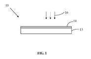
- FIG. 1 is a schematic, side view of a luminescent element according to an embodiment of the present disclosure
- FIG. 2 is a flowchart of an embodiment of a preparation method of a luminescent element
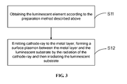
- FIG. 3 is a flowchart of an embodiment of a luminescence method of a luminescent element
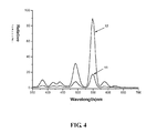
- FIG. 4 is an emission spectrum of the luminescent element of Example 1 comparing with the luminescent glass without the metal layer, the emission spectrum being tested by a spectrometer excited by cathode-ray of 5KV accelerating voltage.
- an embodiment of a luminescent element 10 includes a luminescent substrate 13 and a metal layer 14 formed on a surface of the luminescent substrate 13.
- the metal layer 14 has a metal microstructure, which may be called as micro-nano structure.
- the metal microstructure is aperiodic, i.e. composed of metal crystal in irregular arrangement.
- the luminescent substrate 13 may be a luminescent glass doped with the luminescent material with a chemical composition of Y 2 SiO 5 :Tb.
- the luminescent glass has a composition (by mole parts) of 20Na 2 O-20BaO-30B 2 O 3 -30SiO 2 , which is not limited if glass powder with low melting temperature is used.
- the luminescent material of Y 2 SiO 5 :Tb is 5% ⁇ 35% by weight of the luminescent substrate.
- the luminescent substrate 13 includes a transparent or translucent substrate and a luminescent film formed on the substrate with a chemical composition of Y 2 SiO 5 :Tb, and the metal layer 14 is formed on a surface of the luminescent film.
- the metal layer 14 may be made of metals with excellent chemical stability, such as antioxidant and corrosion-resistant metals, or common metals.
- the metal layer 14 is preferably made of at least one metal selected from the group consisting of Au, Ag, Al, Cu, Ti, Fe, Ni, Co, Cr, Pt, Pd, Mg, and Zn, or more preferably made of at least one metal selected from the group consisting of Au, Ag, and Al.
- the metal layer 14 may be made of one metal or a composite metal.
- the composite metal may be an alloy of two or more than two metals described above.
- the metal layer 14 may be an Ag/Al alloy layer or an Au/Al alloy layer, where the weight percent of Ag or Au is preferably more than 70%.
- the metal layer 14 has a thickness in a range of 0.5 ⁇ 200 nm, preferably 1 ⁇ 100 nm.
- the luminescent element 10 can be widely applied to luminescent devices with ultra-high brightness and high-speed motion, such as field emission display, field emission light source, and large advertising display, etc..
- the anode applies a positive voltage to the field emission cathode to form an accelerating electric field, the cathode emits electron, i.e. cathode-ray 16 to the metal layer 14, so that a surface plasmon is formed between the metal layer 14 and the luminescent substrate 13.
- the internal quantum efficiency of the luminescent substrate 13 is highly increased, and the spontaneous emission of the luminescent glass is highly increased, so that the luminous efficiency of the luminescent glass is improved and the problem of low efficiency of the luminescent materials is overcome.
- a metal layer is formed on the surface of the luminescent substrate 13, a uniform interface is formed between the whole metal layer and the luminescent substrate 13, thus improving the luminescent homogeneity.
- a flow chart of an embodiment of a preparation method of a luminescent element includes following steps:
- the luminescent substrate 13 includes a luminescent material with a chemical composition of Y 2 SiO 5 :Tb.
- Step S02 the metal layer 14 is formed on a surface of the luminescent substrate 13.
- Step S03 the luminescent substrate 13 and the metal layer 14 are annealed in vacuum to form a metal microstructure of the metal layer, and then the luminescent substrate 13 and the metal layer 14 are cooled to form the luminescent element.
- the luminescent substrate 13 accordingly has two types of structure, the first one is the luminescent glass doped with the luminescent material with a chemical composition of Y 2 SiO 5 :Tb, and the second one includes a substrate and a luminescent film of Y 2 SiO 5 :Tb formed on the substrate.
- the preparation of the first type of the luminescent substrate 13 includes: mixing the luminescent material of Y 2 SiO 5 :Tb and glass powder, melting the luminescent material of Y 2 SiO 5 :Tb and glass powder at a temperature in a range of 1000 ⁇ 1300°C; cooling the luminescent material of Y 2 SiO 5 :Tb and glass powder to ambient temperature, and obtaining the luminescent glass doped with the luminescent material of Y 2 SiO 5 :Tb, wherein the luminescent glass has a composition of 20Na 2 O-20BaO-30B 2 O 3 -30SiO 2 .
- the luminescent material of Y 2 SiO 5 :Tb in the form of powder is mixed with glass powder at a weight ratio of 1:19 ⁇ 7 ⁇ 13, so that the luminescent material of Y 2 SiO 5 :Tb is 5% ⁇ 35% by weight of the mixture.
- the mixture is then melt at a temperature of 1000 ⁇ 1300°C and cooled to ambient temperature by pouring on a steel plate, and the luminescent substrate 13 is finally obtained.
- the melting temperature is preferably 1200°C.
- the preparation of the second type of the luminescent substrate 13 includes: selecting a transparent or translucent substrate as a substrate, and forming a luminescent film with a chemical composition of Y 2 SiO 5 :Tb on the substrate.
- the luminescent film of Y 2 SiO 5 :Tb may be deposited on the substrate by magnetron sputtering, electron beam evaporation, chemical vapor deposition, molecular beam epitaxy, pulsed laser deposition, or spray pyrolysis, etc.
- the metal layer 14 is formed by depositing metal source with excellent chemical stability, such as antioxidant and corrosion-resistant metals, or common metals.
- the metal layer 14 is preferably made of at least one metal selected from the group consisting of Au, Ag, Al, Cu, Ti, Fe, Ni, Co, Cr, Pt, Pd, Mg, and Zn, or more preferably made of at least one metal selected from the group consisting of Au, Ag, and Al.
- the metal layer 14 is formed on the surface of the luminescent substrate 13 via PVD or CVD, for example, via sputtering or evaporation, with at least one metal described above.
- the metal layer 14 has a thickness in a range of 0.5 ⁇ 200 nm, preferably 1 ⁇ 100 nm.
- step S03 after the formation of the metal layer 14 on the luminescent substrate 13, the metal layer 14 and the luminescent substrate 13 are annealed at a temperature in a range of 50 ⁇ 650°C for a period of time of 5 minutes to 5 hours and cooled to ambient temperature.
- the preferred anneal temperature is in a range of 100 ⁇ 500°C
- the preferred anneal time is in a range of 15 minutes to 3 hours.
- a flow chart of a luminescence method of the luminescent element includes following steps:
- Step S11 the luminescent element 10 is obtained according to the previously described preparation method.
- Step S12 the cathode-ray 16 is emitted to the metal layer 14.
- a surface plasmon is formed between the metal layer 14 and the luminescent substrate 13 by the radiation of the cathode-ray 16 and thus irradiating the luminescent substrate 13.
- the luminescent element 10 has features of structure and composition as previously described.
- the step S12 can be implemented by field emission display or illumination light source.
- the anode applies a positive voltage to the field emission cathode to form an accelerating electric field, so that the cathode emits cathode-ray 16.
- electron beam will penetrate the metal layer 14 and irradiate the luminescent substrate 13.
- a surface plasmon is formed between the metal layer 14 and the luminescent substrate 13. Due to the surface plasmon effect, the internal quantum efficiency of the luminescent substrate 13 is highly increased, and the spontaneous emission of the luminescent material is highly increased, so that the luminous efficiency of the luminescent material is improved.
- the luminescent substrate 13 accordingly has two types of structure.
- the electron beam will penetrate the metal layer 14 and irradiate the luminescent material of Y 2 SiO 5 :Tb in the luminescent glass, and the surface plasmon is formed between the surface of the luminescent glass doped with the luminescent material of Y 2 SiO 5 :Tb and the metal layer 14, thus irradiating the luminescent material of Y 2 SiO 5 :Tb.
- the electron beam will penetrate the metal layer 14 and irradiate the luminescent film of Y 2 SiO 5 :Tb directly, and the surface plasmon is formed between the luminescent film of Y 2 SiO 5 :Tb and the metal layer 14, thus irradiating the luminescent film of Y 2 SiO 5 :Tb.
- SPP surface plasmon polaritons
- the electromagnetic field caused by the SPPs can not only constrain the spread of the light wave in sub-wavelength size structure, but also can produce and manipulate the electromagnetic radiation from light frequency to microwave band, thus active manipulation of the light spread is implemented. Accordingly, the present embodiment uses the excitation of the SPPs to increase the optical density of the luminescent glass and to enhance spontaneous emission velocity of the luminescent glass.
- the coupling effect of the surface plasmon can be used, when the luminescent glass irradiates, sympathetic vibration phenomena occurs, thus the internal quantum efficiency of the luminescent glass is highly increased, so that the luminous efficiency of the luminescent glass is improved.
- Y 2 SiO 5 :Tb can be utilized from a commercial product.
- Phosphor with the composition of Y 2 SiO 5 :Tb is mixed with glass powder with the composition of 20Na 2 O-20BaO-30B 2 O 3 -30SiO 2 in a weight ratio of 1:4, and the mixture is melt to obtain the luminescent glass doped with the luminescent material of Y 2 SiO 5 :Tb.
- a silver layer with a thickness of 2 nm is deposited on the surface of the luminescent glass via a magnetron sputtering equipment.
- the luminescent substrate and the silver layer are annealed at a temperature of 300°C for half an hour in vacuum with the vacuum degree ⁇ 1 ⁇ 10 -3 Pa and cooled to ambient temperature, thus a luminescent element is obtained.
- the prepared luminescent element is bombarded by cathode-ray emitted from an electron gun, and the electron beam penetrates the metal layer and irradiates the luminescent glass doped with the luminescent material of Y 2 SiO 5 :Tb, thus an emission spectrum shown in FIG. 4 is obtained, which shows that the luminescent material emits green light.
- curve 11 represents an emission spectrum of a luminescent glass without the metal layer
- curve 12 represents an emission spectrum of the luminescent element with the metal layer of Example 1.
- the luminescent element with the metal layer of Example 1 has a luminescence integral intensity 4 times as that of the luminescent glass without the metal layer in a wavelength of 350 ⁇ 700 nm, accordingly, the luminescent performance is greatly improved.
- Example 1 has the similar emission spectrums and luminescent performance as Example 1, which will not be described later.
- Phosphor with the composition of Y 2 SiO 5 :Tb is mixed with glass powder with the composition of 20Na 2 O-20BaO-30B 2 O 3 -30SiO 2 in a weight ratio of 1:19, and the mixture is melt to obtain the luminescent glass doped with the luminescent material of Y 2 SiO 5 :Tb.
- a gold layer with a thickness of 0.5 nm is deposited on the surface of the luminescent glass via a magnetron sputtering equipment.
- the luminescent substrate and the gold layer are annealed at a temperature of 200°C for one hour in vacuum with the vacuum degree ⁇ 1 ⁇ 10 -3 Pa and cooled to ambient temperature, thus a luminescent element is obtained.
- Phosphor with the composition of Y 2 SiO 5 :Tb is mixed with glass powder with the composition of 20Na 2 O-20BaO-30B 2 O 3 -30SiO 2 in a weight ratio of 7:13, and the mixture is melt to obtain the luminescent glass doped with the luminescent material of Y 2 SiO 5 :Tb.
- An aluminum layer with a thickness of 200nm is deposited on the surface of the luminescent glass via a magnetron sputtering equipment. The luminescent glass and the aluminum layer are annealed at a temperature of 500°C for 5 hours in vacuum with the vacuum degree ⁇ 1 ⁇ 10 -3 Pa and cooled to ambient temperature, thus a luminescent element is obtained.
- a 1 ⁇ 1 cm 2 , double-sided polished, sapphire substrate is selected, and a luminescent film with the chemical composition of Y 2 SiO 5 :Tb is formed on the substrate via magnetron sputtering.
- a magnesium layer with a thickness of 100nm is deposited on the surface of the luminescent glass via an electron beam evaporation equipment.
- the luminescent substrate and the magnesium layer are annealed at a temperature of 650°C for 5 minutes in vacuum with the vacuum degree ⁇ 1 ⁇ 10 -3 Pa and cooled to ambient temperature, thus a luminescent element is obtained.
- a 1 ⁇ 1 cm 2 , double-sided polished, magnesium oxide substrate is selected, and a luminescent film with the chemical composition of Y 2 SiO 5 :Tb is formed on the substrate via molecular beam epitaxy.
- a palladium layer with a thickness of 1nm is deposited on the surface of the luminescent glass via an electron beam evaporation equipment.
- the luminescent glass and the palladium layer are annealed at a temperature of 100°C for 3 hours in vacuum with the vacuum degree ⁇ 1 ⁇ 10 -3 Pa and cooled to ambient temperature, thus a luminescent element is obtained.
- a 1 ⁇ 1 cm 2 , double-sided polished, magnesium oxide substrate is selected, and a luminescent film with the chemical composition of Y 2 SiO 5 :Tb is formed on the substrate via spray pyrolysis.
- a platinum layer with a thickness of 5nm is deposited on the surface of the luminescent glass via an electron beam evaporation equipment. The luminescent glass and the platinum layer are annealed at a temperature of 450°C for 15 minutes in vacuum with the vacuum degree ⁇ 1 ⁇ 10 -3 Pa and cooled to ambient temperature, thus a luminescent element is obtained.
- a 1 ⁇ 1 cm 2 , double-sided polished, quartz substrate is selected, and a luminescent film with the chemical composition of Y 2 SiO 5 :Tb is formed on the substrate via magnetron sputtering.
- An iron layer with a thickness of 20nm is deposited on the surface of the luminescent glass via an electron beam evaporation equipment.
- the luminescent glass and the iron layer are annealed at a temperature of 50°C for 5 hours in vacuum with the vacuum degree ⁇ 1 ⁇ 10 -3 Pa and cooled to ambient temperature, thus a luminescent element is obtained.
- a 1 ⁇ cm 2 , double-sided polished, quartz substrate is selected, and a luminescent film with the chemical composition of Y 2 SiO 5 :Tb is formed on the substrate via magnetron sputtering.
- a titanium layer with a thickness of 10nm is deposited on the surface of the luminescent glass via an electron beam evaporation equipment. The luminescent glass and the titanium layer are annealed at a temperature of 150°C for 2 hours in vacuum with the vacuum degree ⁇ 1 ⁇ 10 -3 Pa and cooled to ambient temperature, thus a luminescent element is obtained.
- a 1 ⁇ 1 cm 2 , double-sided polished, quartz substrate is selected, and a luminescent film with the chemical composition of Y 2 SiO 5 :Tb is formed on the substrate via magnetron sputtering.
- a copper layer with a thickness of 50nm is deposited on the surface of the luminescent glass via an electron beam evaporation equipment.
- the luminescent glass and the copper layer are annealed at a temperature of 200°C for 2.5 hours in vacuum with the vacuum degree ⁇ 1 ⁇ 10 -3 Pa and cooled to ambient temperature, thus a luminescent element is obtained.
- a 1 ⁇ 1 cm 2 , double-sided polished, quartz substrate is selected, and a luminescent film with the chemical composition of Y 2 SiO 5 :Tb is formed on the substrate via magnetron sputtering.
- a zinc layer with a thickness of 150nm is deposited on the surface of the luminescent glass via an electron beam evaporation equipment.
- the luminescent glass and the zinc layer are annealed at a temperature of 350°C for 0.5 hour in vacuum with the vacuum degree ⁇ 1 ⁇ 10 -3 Pa and cooled to ambient temperature, thus a luminescent element is obtained.
- a 1 ⁇ cm 2 , double-sided polished, quartz substrate is selected, and a luminescent film with the chemical composition of Y 2 SiO 5 :Tb is formed on the substrate via magnetron sputtering.
- a chromium layer with a thickness of 120nm is deposited on the surface of the luminescent glass via an electron beam evaporation equipment. The luminescent glass and the chromium layer are annealed at a temperature of 250°C for 2 hours in vacuum with the vacuum degree ⁇ 1 ⁇ 10 -3 Pa and cooled to ambient temperature, thus a luminescent element is obtained.
- a 1 ⁇ 1 cm 2 , double-sided polished, quartz substrate is selected, and a luminescent film with the chemical composition of Y 2 SiO 5 :Tb is formed on the substrate via magnetron sputtering.
- a nickel layer with a thickness of 40nm is deposited on the surface of the luminescent glass via an electron beam evaporation equipment. The luminescent glass and the nickel layer are annealed at a temperature of 80°C for 4 hours in vacuum with the vacuum degree ⁇ 1 ⁇ 10 -3 Pa and cooled to ambient temperature, thus a luminescent element is obtained.
- a 1 ⁇ 1 cm 2 , double-sided polished, quartz substrate is selected, and a luminescent film with the chemical composition of Y 2 SiO 5 :Tb is formed on the substrate via magnetron sputtering.
- a cobalt layer with a thickness of 180nm is deposited on the surface of the luminescent glass via an electron beam evaporation equipment.
- the luminescent glass and the cobalt layer are annealed at a temperature of 400°C for 1 hour in vacuum with the vacuum degree ⁇ 1 ⁇ 10 -3 Pa and cooled to ambient temperature, thus a luminescent element is obtained.
- Phosphor with the composition of Y 2 SiO 5 :Tb is mixed with glass powder with the composition of 20Na 2 O-20BaO-30B 2 O 3 -30SiO 2 in a weight ratio of 3:17, and the mixture is melt to obtain the luminescent glass doped with the luminescent material of Y 2 SiO 5 :Tb.
- a gold/aluminum layer with a thickness of 0.5nm is deposited on the surface of the luminescent glass via an electron beam evaporation equipment. In the gold/aluminum layer, the gold is about 80 weight %, and the aluminum is about 20 weight %.
- the luminescent glass and the gold/aluminum layer are annealed at a temperature of 200°C for 1 hour in vacuum with the vacuum degree ⁇ 1 ⁇ 10 -3 Pa and cooled to ambient temperature, thus a luminescent element is obtained.
- Phosphor with the composition of Y 2 SiO 5 :Tb is mixed with glass powder with the composition of 20Na 2 O-20BaO-30B 2 O 3 -30SiO 2 in a weight ratio of 3: 7, and the mixture is melt to obtain the luminescent glass doped with the luminescent material of Y 2 SiO 5 :Tb.
- a silver/aluminum layer with a thickness of 15nm is deposited on the surface of the luminescent glass via a magnetron sputtering equipment. In the silver/aluminum layer, the silver is about 90 weight %, and the aluminum is about 10 weight %.
- the luminescent glass and the silver/aluminum layer are annealed at a temperature of 200°C for 1 hour in vacuum with the vacuum degree ⁇ 1 ⁇ 10 -3 Pa and cooled to ambient temperature, thus a luminescent element is obtained.
- a 1 ⁇ 1 cm 2 , double-sided polished, quartz substrate is selected, and a luminescent film with the chemical composition of Y 2 SiO 5 :Tb is formed on the substrate via magnetron sputtering.
- a silver/aluminum layer with a thickness of 10nm is deposited on the surface of the luminescent glass via an electron beam evaporation equipment. In the silver/aluminum layer, the silver is about 80 weight %, and the aluminum is about 20 weight %.
- the luminescent glass and the silver/aluminum layer are annealed at a temperature of 150°C for 2 hours in vacuum with the vacuum degree ⁇ 1 ⁇ 10 -3 Pa and cooled to ambient temperature, thus a luminescent element is obtained.
- a 1 ⁇ 1 cm 2 , double-sided polished, magnesium oxide substrate is selected, and a luminescent film with the chemical composition of Y 2 SiO 5 :Tb is formed on the substrate via magnetron sputtering.
- a gold/aluminum layer with a thickness of 0.5nm is deposited on the surface of the luminescent glass via a magnetron sputtering equipment. In the gold/aluminum layer, the gold is about 90 weight %, and the aluminum is about 10 weight %.
- the luminescent glass and the gold/aluminum layer are annealed at a temperature of 120°C for 2 hours in vacuum with the vacuum degree ⁇ 1 ⁇ 10 -3 Pa and cooled to ambient temperature, thus a luminescent element is obtained.
- the metal layer 14 with a metal microstructure is formed on a surface of the luminescent substrate 13, and when irradiated by the cathode-ray, a surface plasmon can be formed between the metal layer 14 and the luminescent substrate 13. Due to the surface plasmon effect, the internal quantum efficiency of the luminescent substrate 13 is highly increased, and the spontaneous emission of the luminescent glass is highly increased, so that the luminous efficiency of the luminescent glass is improved and the problem of low efficiency of the luminescent materials is overcome. In the luminescence method of the luminescent element, once emitting cathode-ray to the metal layer 14, the surface plasmon will be formed between the metal layer 14 and the luminescent substrate 13, thus improving the luminous efficiency and reliability.
- the luminescent element 10 has a simple two-layer structure for including the luminescent substrate 13 and the metal layer 14. In addition, there is a uniform interface formed between the luminescent substrate 13 and the metal layer 14, so that an excellent luminescent homogeneity and stability is achieved. In the luminescence method of the luminescent element, once emitting cathode-ray to the metal layer 14, the surface plasmon will be formed between the metal layer 14 and the luminescent substrate 13, thus improving the luminous efficiency and reliability of the luminescent substrate 13.
- the luminescent element can be obtained by forming a metal layer 14 on the luminescent substrate 13 and annealing the luminescent substrate 13 and the metal layer 14, thus the preparation method is simple and has a low cost.
- the luminescent element can be widely applied to luminescent devices with ultra-high brightness and high-speed motion, such as field emission display.
Abstract
Description
- The present disclosure relates to luminescent materials, and more particularly relates to a luminescent element including a glass substrate made of luminescent material, preparation method thereof and luminescence method.
- The conventional materials used as luminescent substrate include phosphor, nanocrystal, glass, etc. Comparing to the crystal and phosphor, the glass is transparent, rigid, and has excellent chemical stability and superior luminescent performance. In addition, the glass can be easily machined into products with various shapes, such as display devices or luminescent light sources with various shapes and sizes.
- For example, in vacuum microelectronics, field emission devices usually use luminescent glass as illuminant, which has shown a wide prospect in illumination and display techniques and draws a lot attention to domestic and foreign research institutes. The working principle of the field emission device is that, in vacuum, the anode applies a positive voltage to the field emissive arrays (FEAs) to form an accelerating electric field, electron emitted from the cathode accelerately bombards the luminescent material on the anode plate to irradiate. The field emission device has a wide operating temperature range (-40°C∼80°C), short corresponding time (<1ms), simple structure, low energy consumption and meets the environmental protection requirements. Furthermore, materials such as the phosphor, luminescent glass, luminescent film, etc., can be served as luminescent material in field emission device, however, they all suffer from serious problems of low luminous efficiency, thus significantly limit the application of the field emission device, especially in the application of illumination.
- In one aspect of the present disclosure, a luminescent element with a high luminescent homogeneity, high luminous efficiency, good stability, simple structure and a preparation method with a simple processes and low cost are desired.
- In another aspect of the present disclosure, a luminescence method of the luminescent element with simple operation, good reliability, and high luminous efficiency is also desired.
- A luminescent element includes: a luminescent substrate; and a metal layer with a metal microstructure formed on a surface of the luminescent substrate; wherein the luminescent substrate comprises a luminescent material with a chemical composition of Y2SiO5:Tb.
- A preparation method of a luminescent element includes:
- preparing a luminescent substrate comprising a luminescent material with a chemical composition of Y2SiO5:Tb;
- forming a metal layer on the luminescent substrate, and
- annealing the luminescent substrate and the metal layer in vacuum to form a metal microstructure of the metal layer, and then cooling the luminescent substrate and the metal layer to form the luminescent element.
- A luminescence method of a luminescent element includes:
- obtaining the luminescent element according to the preparation method described above; and
- emitting cathode-ray to the metal layer, forming a surface plasmon between the metal layer and the luminescent substrate by the radiation of the cathode-ray and then irradiating the luminescent substrate.
- In the luminescent element described above, the metal layer with a metal microstructure is formed on a surface of the luminescent substrate, and when irradiated by the cathode-ray, a surface plasmon can be formed between the metal layer and the luminescent substrate. Due to the surface plasmon effect, the internal quantum efficiency of the luminescent substrate is highly increased, and the spontaneous emission of the luminescent substrate is highly increased, so that the luminous efficiency of the luminescent substrate is improved and the problem of low efficiency of the luminescent materials is overcome. Accordingly, in the luminescence method of the luminescent element, once emitting cathode-ray to the metal layer, the surface plasmon will be formed between the metal layer and the luminescent substrate, thus improving the luminous efficiency and reliability. The luminescent element has a simple two-layer structure for including the luminescent substrate and the metal layer. In addition, there is a uniform interface formed between the luminescent substrate and the metal layer, so that an excellent luminescent homogeneity and stability is achieved. In the luminescence method of the luminescent element, once emitting cathode-ray to the metal layer, the surface plasmon will be formed between the metal layer and the luminescent substrate, thus improving the luminous efficiency and reliability of the luminescent substrate.
- In the embodiment of the preparation method of the luminescent element, the luminescent element can be obtained by forming a metal layer on the luminescent substrate and annealing the luminescent substrate and the metal layer, thus the preparation method is simple and has a low cost and wide application prospects.
- The components in the drawings are not necessarily drawn to scale, the emphasis instead being placed upon clearly illustrating the principles of the present disclosure. Moreover, in the drawings, like reference numerals designate corresponding parts throughout the views.
-
FIG. 1 is a schematic, side view of a luminescent element according to an embodiment of the present disclosure; -
FIG. 2 is a flowchart of an embodiment of a preparation method of a luminescent element; -
FIG. 3 is a flowchart of an embodiment of a luminescence method of a luminescent element; -
FIG. 4 is an emission spectrum of the luminescent element of Example 1 comparing with the luminescent glass without the metal layer, the emission spectrum being tested by a spectrometer excited by cathode-ray of 5KV accelerating voltage. - The disclosure is illustrated by way of example and not by way of limitation in the figures of the accompanying drawings in which like references indicate similar elements. It should be noted that references to "an" or "one" embodiment in this disclosure are not necessarily to the same embodiment, and such references mean at least one.
- Referring to
FIG. 1 , an embodiment of aluminescent element 10 includes aluminescent substrate 13 and ametal layer 14 formed on a surface of theluminescent substrate 13. Themetal layer 14 has a metal microstructure, which may be called as micro-nano structure. In addition, the metal microstructure is aperiodic, i.e. composed of metal crystal in irregular arrangement. - In one embodiment, the
luminescent substrate 13 may be a luminescent glass doped with the luminescent material with a chemical composition of Y2SiO5:Tb. The luminescent glass has a composition (by mole parts) of 20Na2O-20BaO-30B2O3-30SiO2, which is not limited if glass powder with low melting temperature is used. The luminescent material of Y2SiO5:Tb is 5%∼35% by weight of the luminescent substrate. - In an alternative embodiment, the
luminescent substrate 13 includes a transparent or translucent substrate and a luminescent film formed on the substrate with a chemical composition of Y2SiO5:Tb, and themetal layer 14 is formed on a surface of the luminescent film. - The
metal layer 14 may be made of metals with excellent chemical stability, such as antioxidant and corrosion-resistant metals, or common metals. Themetal layer 14 is preferably made of at least one metal selected from the group consisting of Au, Ag, Al, Cu, Ti, Fe, Ni, Co, Cr, Pt, Pd, Mg, and Zn, or more preferably made of at least one metal selected from the group consisting of Au, Ag, and Al. Themetal layer 14 may be made of one metal or a composite metal. The composite metal may be an alloy of two or more than two metals described above. For example, themetal layer 14 may be an Ag/Al alloy layer or an Au/Al alloy layer, where the weight percent of Ag or Au is preferably more than 70%. Themetal layer 14 has a thickness in a range of 0.5∼200 nm, preferably 1∼100 nm. - As a luminescent element, the
luminescent element 10 can be widely applied to luminescent devices with ultra-high brightness and high-speed motion, such as field emission display, field emission light source, and large advertising display, etc.. Take field emission display as an example, the anode applies a positive voltage to the field emission cathode to form an accelerating electric field, the cathode emits electron, i.e. cathode-ray 16 to themetal layer 14, so that a surface plasmon is formed between themetal layer 14 and theluminescent substrate 13. Due to the surface plasmon effect, the internal quantum efficiency of theluminescent substrate 13 is highly increased, and the spontaneous emission of the luminescent glass is highly increased, so that the luminous efficiency of the luminescent glass is improved and the problem of low efficiency of the luminescent materials is overcome. In addition, since a metal layer is formed on the surface of theluminescent substrate 13, a uniform interface is formed between the whole metal layer and theluminescent substrate 13, thus improving the luminescent homogeneity. - Referring to
FIG. 1 andFIG. 2 , a flow chart of an embodiment of a preparation method of a luminescent element includes following steps: - Step S01, the
luminescent substrate 13 is prepared. Theluminescent substrate 13 includes a luminescent material with a chemical composition of Y2SiO5:Tb. - Step S02, the
metal layer 14 is formed on a surface of theluminescent substrate 13. - Step S03, the
luminescent substrate 13 and themetal layer 14 are annealed in vacuum to form a metal microstructure of the metal layer, and then theluminescent substrate 13 and themetal layer 14 are cooled to form the luminescent element. - In the step S01, the
luminescent substrate 13 accordingly has two types of structure, the first one is the luminescent glass doped with the luminescent material with a chemical composition of Y2SiO5:Tb, and the second one includes a substrate and a luminescent film of Y2SiO5:Tb formed on the substrate. The preparation of the first type of theluminescent substrate 13 includes: mixing the luminescent material of Y2SiO5:Tb and glass powder, melting the luminescent material of Y2SiO5:Tb and glass powder at a temperature in a range of 1000∼1300°C; cooling the luminescent material of Y2SiO5:Tb and glass powder to ambient temperature, and obtaining the luminescent glass doped with the luminescent material of Y2SiO5:Tb, wherein the luminescent glass has a composition of 20Na2O-20BaO-30B2O3-30SiO2. In detail, The luminescent material of Y2SiO5:Tb in the form of powder is mixed with glass powder at a weight ratio of 1:19∼7∼13, so that the luminescent material of Y2SiO5:Tb is 5%∼35% by weight of the mixture. The mixture is then melt at a temperature of 1000∼1300°C and cooled to ambient temperature by pouring on a steel plate, and theluminescent substrate 13 is finally obtained. The melting temperature is preferably 1200°C. - The preparation of the second type of the
luminescent substrate 13 includes: selecting a transparent or translucent substrate as a substrate, and forming a luminescent film with a chemical composition of Y2SiO5:Tb on the substrate. The luminescent film of Y2SiO5:Tb may be deposited on the substrate by magnetron sputtering, electron beam evaporation, chemical vapor deposition, molecular beam epitaxy, pulsed laser deposition, or spray pyrolysis, etc. - As previously described, the
metal layer 14 is formed by depositing metal source with excellent chemical stability, such as antioxidant and corrosion-resistant metals, or common metals. Themetal layer 14 is preferably made of at least one metal selected from the group consisting of Au, Ag, Al, Cu, Ti, Fe, Ni, Co, Cr, Pt, Pd, Mg, and Zn, or more preferably made of at least one metal selected from the group consisting of Au, Ag, and Al. In step S02, themetal layer 14 is formed on the surface of theluminescent substrate 13 via PVD or CVD, for example, via sputtering or evaporation, with at least one metal described above. Themetal layer 14 has a thickness in a range of 0.5∼200 nm, preferably 1∼100 nm. - In step S03, after the formation of the
metal layer 14 on theluminescent substrate 13, themetal layer 14 and theluminescent substrate 13 are annealed at a temperature in a range of 50∼650°C for a period of time of 5 minutes to 5 hours and cooled to ambient temperature. The preferred anneal temperature is in a range of 100∼500°C, and the preferred anneal time is in a range of 15 minutes to 3 hours. - Referring to
FIG. 1 andFIG. 3 , a flow chart of a luminescence method of the luminescent element includes following steps: - Step S11, the
luminescent element 10 is obtained according to the previously described preparation method. - Step S12, the cathode-
ray 16 is emitted to themetal layer 14. A surface plasmon is formed between themetal layer 14 and theluminescent substrate 13 by the radiation of the cathode-ray 16 and thus irradiating theluminescent substrate 13. - The
luminescent element 10 has features of structure and composition as previously described. In application, the step S12 can be implemented by field emission display or illumination light source. In vacuum, the anode applies a positive voltage to the field emission cathode to form an accelerating electric field, so that the cathode emits cathode-ray 16. Excited by the cathode-ray 16, electron beam will penetrate themetal layer 14 and irradiate theluminescent substrate 13. During such process, a surface plasmon is formed between themetal layer 14 and theluminescent substrate 13. Due to the surface plasmon effect, the internal quantum efficiency of theluminescent substrate 13 is highly increased, and the spontaneous emission of the luminescent material is highly increased, so that the luminous efficiency of the luminescent material is improved. - As previously described, the
luminescent substrate 13 accordingly has two types of structure. In the first type, the electron beam will penetrate themetal layer 14 and irradiate the luminescent material of Y2SiO5:Tb in the luminescent glass, and the surface plasmon is formed between the surface of the luminescent glass doped with the luminescent material of Y2SiO5:Tb and themetal layer 14, thus irradiating the luminescent material of Y2SiO5:Tb. In the second type, the electron beam will penetrate themetal layer 14 and irradiate the luminescent film of Y2SiO5:Tb directly, and the surface plasmon is formed between the luminescent film of Y2SiO5:Tb and themetal layer 14, thus irradiating the luminescent film of Y2SiO5:Tb. - Surface plasmon (SP) is a wave spread along the interface between the metal and medium, whose amplitude exponentially decay with the increase of the distance away from the interface. When changing a surface structure of the metal, the feature, dispersion relationship, excitation mode, coupling effect of the surface plasmon polaritons (SPPs) will be significantly changed. The electromagnetic field caused by the SPPs can not only constrain the spread of the light wave in sub-wavelength size structure, but also can produce and manipulate the electromagnetic radiation from light frequency to microwave band, thus active manipulation of the light spread is implemented. Accordingly, the present embodiment uses the excitation of the SPPs to increase the optical density of the luminescent glass and to enhance spontaneous emission velocity of the luminescent glass. In addition, the coupling effect of the surface plasmon can be used, when the luminescent glass irradiates, sympathetic vibration phenomena occurs, thus the internal quantum efficiency of the luminescent glass is highly increased, so that the luminous efficiency of the luminescent glass is improved.
- A plurality of examples are described to illustrate the different compositions and preparation methods of the luminescent element, and their performances. In the examples, Y2SiO5:Tb can be utilized from a commercial product.
- Example 1
- Phosphor with the composition of Y2SiO5:Tb is mixed with glass powder with the composition of 20Na2O-20BaO-30B2O3-30SiO2 in a weight ratio of 1:4, and the mixture is melt to obtain the luminescent glass doped with the luminescent material of Y2SiO5:Tb. A silver layer with a thickness of 2 nm is deposited on the surface of the luminescent glass via a magnetron sputtering equipment. The luminescent substrate and the silver layer are annealed at a temperature of 300°C for half an hour in vacuum with the vacuum degree <1×10⁻³ Pa and cooled to ambient temperature, thus a luminescent element is obtained.
- During the spectroscopy test, the prepared luminescent element is bombarded by cathode-ray emitted from an electron gun, and the electron beam penetrates the metal layer and irradiates the luminescent glass doped with the luminescent material of Y2SiO5:Tb, thus an emission spectrum shown in
FIG. 4 is obtained, which shows that the luminescent material emits green light. InFIG. 4 ,curve 11 represents an emission spectrum of a luminescent glass without the metal layer;curve 12 represents an emission spectrum of the luminescent element with the metal layer of Example 1. As shown inFIG. 4 , since a surface plasmon is formed between the metal layer and the luminescent glass, comparing to the luminescent glass without the metal layer, the luminescent element with the metal layer of Example 1 has a luminescence integral intensity 4 times as that of the luminescent glass without the metal layer in a wavelength of 350∼700 nm, accordingly, the luminescent performance is greatly improved. - Other Examples have the similar emission spectrums and luminescent performance as Example 1, which will not be described later.
- Example 2
- Phosphor with the composition of Y2SiO5:Tb is mixed with glass powder with the composition of 20Na2O-20BaO-30B2O3-30SiO2 in a weight ratio of 1:19, and the mixture is melt to obtain the luminescent glass doped with the luminescent material of Y2SiO5:Tb. A gold layer with a thickness of 0.5 nm is deposited on the surface of the luminescent glass via a magnetron sputtering equipment. The luminescent substrate and the gold layer are annealed at a temperature of 200°C for one hour in vacuum with the vacuum degree <1 × 10⁻³ Pa and cooled to ambient temperature, thus a luminescent element is obtained.
- Example 3
- Phosphor with the composition of Y2SiO5:Tb is mixed with glass powder with the composition of 20Na2O-20BaO-30B2O3-30SiO2 in a weight ratio of 7:13, and the mixture is melt to obtain the luminescent glass doped with the luminescent material of Y2SiO5:Tb. An aluminum layer with a thickness of 200nm is deposited on the surface of the luminescent glass via a magnetron sputtering equipment. The luminescent glass and the aluminum layer are annealed at a temperature of 500°C for 5 hours in vacuum with the vacuum degree <1 × 10⁻³ Pa and cooled to ambient temperature, thus a luminescent element is obtained.
- Example 4
- A 1 × 1 cm2, double-sided polished, sapphire substrate is selected, and a luminescent film with the chemical composition of Y2SiO5:Tb is formed on the substrate via magnetron sputtering. A magnesium layer with a thickness of 100nm is deposited on the surface of the luminescent glass via an electron beam evaporation equipment. The luminescent substrate and the magnesium layer are annealed at a temperature of 650°C for 5 minutes in vacuum with the vacuum degree <1 × 10⁻³ Pa and cooled to ambient temperature, thus a luminescent element is obtained.
- Example 5
- A 1 × 1 cm2, double-sided polished, magnesium oxide substrate is selected, and a luminescent film with the chemical composition of Y2SiO5:Tb is formed on the substrate via molecular beam epitaxy. A palladium layer with a thickness of 1nm is deposited on the surface of the luminescent glass via an electron beam evaporation equipment. The luminescent glass and the palladium layer are annealed at a temperature of 100°C for 3 hours in vacuum with the vacuum degree <1 × 10⁻³ Pa and cooled to ambient temperature, thus a luminescent element is obtained.
- Example 6
- A 1 × 1 cm2, double-sided polished, magnesium oxide substrate is selected, and a luminescent film with the chemical composition of Y2SiO5:Tb is formed on the substrate via spray pyrolysis. A platinum layer with a thickness of 5nm is deposited on the surface of the luminescent glass via an electron beam evaporation equipment. The luminescent glass and the platinum layer are annealed at a temperature of 450°C for 15 minutes in vacuum with the vacuum degree <1 × 10⁻³ Pa and cooled to ambient temperature, thus a luminescent element is obtained.
- Example 7
- A 1 × 1 cm2, double-sided polished, quartz substrate is selected, and a luminescent film with the chemical composition of Y2SiO5:Tb is formed on the substrate via magnetron sputtering. An iron layer with a thickness of 20nm is deposited on the surface of the luminescent glass via an electron beam evaporation equipment. The luminescent glass and the iron layer are annealed at a temperature of 50°C for 5 hours in vacuum with the vacuum degree <1 × 10⁻³ Pa and cooled to ambient temperature, thus a luminescent element is obtained.
- Example 8
- A 1 × cm2, double-sided polished, quartz substrate is selected, and a luminescent film with the chemical composition of Y2SiO5:Tb is formed on the substrate via magnetron sputtering. A titanium layer with a thickness of 10nm is deposited on the surface of the luminescent glass via an electron beam evaporation equipment. The luminescent glass and the titanium layer are annealed at a temperature of 150°C for 2 hours in vacuum with the vacuum degree <1 × 10⁻³ Pa and cooled to ambient temperature, thus a luminescent element is obtained.
- Example 9
- A 1 × 1 cm2, double-sided polished, quartz substrate is selected, and a luminescent film with the chemical composition of Y2SiO5:Tb is formed on the substrate via magnetron sputtering. A copper layer with a thickness of 50nm is deposited on the surface of the luminescent glass via an electron beam evaporation equipment. The luminescent glass and the copper layer are annealed at a temperature of 200°C for 2.5 hours in vacuum with the vacuum degree <1 × 10⁻³ Pa and cooled to ambient temperature, thus a luminescent element is obtained.
- Example 10
- A 1 × 1 cm2, double-sided polished, quartz substrate is selected, and a luminescent film with the chemical composition of Y2SiO5:Tb is formed on the substrate via magnetron sputtering. A zinc layer with a thickness of 150nm is deposited on the surface of the luminescent glass via an electron beam evaporation equipment. The luminescent glass and the zinc layer are annealed at a temperature of 350°C for 0.5 hour in vacuum with the vacuum degree <1 × 10⁻³ Pa and cooled to ambient temperature, thus a luminescent element is obtained.
- Example 11
- A 1 × cm2, double-sided polished, quartz substrate is selected, and a luminescent film with the chemical composition of Y2SiO5:Tb is formed on the substrate via magnetron sputtering. A chromium layer with a thickness of 120nm is deposited on the surface of the luminescent glass via an electron beam evaporation equipment. The luminescent glass and the chromium layer are annealed at a temperature of 250°C for 2 hours in vacuum with the vacuum degree <1 × 10⁻³ Pa and cooled to ambient temperature, thus a luminescent element is obtained.
- Example 12
- A 1 × 1 cm2, double-sided polished, quartz substrate is selected, and a luminescent film with the chemical composition of Y2SiO5:Tb is formed on the substrate via magnetron sputtering. A nickel layer with a thickness of 40nm is deposited on the surface of the luminescent glass via an electron beam evaporation equipment. The luminescent glass and the nickel layer are annealed at a temperature of 80°C for 4 hours in vacuum with the vacuum degree <1 × 10⁻³ Pa and cooled to ambient temperature, thus a luminescent element is obtained.
- Example 13
- A 1 × 1 cm2, double-sided polished, quartz substrate is selected, and a luminescent film with the chemical composition of Y2SiO5:Tb is formed on the substrate via magnetron sputtering. A cobalt layer with a thickness of 180nm is deposited on the surface of the luminescent glass via an electron beam evaporation equipment. The luminescent glass and the cobalt layer are annealed at a temperature of 400°C for 1 hour in vacuum with the vacuum degree <1 × 10⁻³ Pa and cooled to ambient temperature, thus a luminescent element is obtained.
- Example 14
- Phosphor with the composition of Y2SiO5:Tb is mixed with glass powder with the composition of 20Na2O-20BaO-30B2O3-30SiO2 in a weight ratio of 3:17, and the mixture is melt to obtain the luminescent glass doped with the luminescent material of Y2SiO5:Tb. A gold/aluminum layer with a thickness of 0.5nm is deposited on the surface of the luminescent glass via an electron beam evaporation equipment. In the gold/aluminum layer, the gold is about 80 weight %, and the aluminum is about 20 weight %. The luminescent glass and the gold/aluminum layer are annealed at a temperature of 200°C for 1 hour in vacuum with the vacuum degree <1 × 10⁻³ Pa and cooled to ambient temperature, thus a luminescent element is obtained.
- Example 15
- Phosphor with the composition of Y2SiO5:Tb is mixed with glass powder with the composition of 20Na2O-20BaO-30B2O3-30SiO2 in a weight ratio of 3: 7, and the mixture is melt to obtain the luminescent glass doped with the luminescent material of Y2SiO5:Tb. A silver/aluminum layer with a thickness of 15nm is deposited on the surface of the luminescent glass via a magnetron sputtering equipment. In the silver/aluminum layer, the silver is about 90 weight %, and the aluminum is about 10 weight %. The luminescent glass and the silver/aluminum layer are annealed at a temperature of 200°C for 1 hour in vacuum with the vacuum degree <1 × 10⁻³ Pa and cooled to ambient temperature, thus a luminescent element is obtained.
- Example 16
- A 1 × 1 cm2, double-sided polished, quartz substrate is selected, and a luminescent film with the chemical composition of Y2SiO5:Tb is formed on the substrate via magnetron sputtering. A silver/aluminum layer with a thickness of 10nm is deposited on the surface of the luminescent glass via an electron beam evaporation equipment. In the silver/aluminum layer, the silver is about 80 weight %, and the aluminum is about 20 weight %. The luminescent glass and the silver/aluminum layer are annealed at a temperature of 150°C for 2 hours in vacuum with the vacuum degree <1 × 10⁻³ Pa and cooled to ambient temperature, thus a luminescent element is obtained.
- Example 17
- A 1 × 1 cm2, double-sided polished, magnesium oxide substrate is selected, and a luminescent film with the chemical composition of Y2SiO5:Tb is formed on the substrate via magnetron sputtering. A gold/aluminum layer with a thickness of 0.5nm is deposited on the surface of the luminescent glass via a magnetron sputtering equipment. In the gold/aluminum layer, the gold is about 90 weight %, and the aluminum is about 10 weight %. The luminescent glass and the gold/aluminum layer are annealed at a temperature of 120°C for 2 hours in vacuum with the vacuum degree <1 × 10⁻³ Pa and cooled to ambient temperature, thus a luminescent element is obtained.
- In Examples described above, the
metal layer 14 with a metal microstructure is formed on a surface of theluminescent substrate 13, and when irradiated by the cathode-ray, a surface plasmon can be formed between themetal layer 14 and theluminescent substrate 13. Due to the surface plasmon effect, the internal quantum efficiency of theluminescent substrate 13 is highly increased, and the spontaneous emission of the luminescent glass is highly increased, so that the luminous efficiency of the luminescent glass is improved and the problem of low efficiency of the luminescent materials is overcome. In the luminescence method of the luminescent element, once emitting cathode-ray to themetal layer 14, the surface plasmon will be formed between themetal layer 14 and theluminescent substrate 13, thus improving the luminous efficiency and reliability. Theluminescent element 10 has a simple two-layer structure for including theluminescent substrate 13 and themetal layer 14. In addition, there is a uniform interface formed between theluminescent substrate 13 and themetal layer 14, so that an excellent luminescent homogeneity and stability is achieved. In the luminescence method of the luminescent element, once emitting cathode-ray to themetal layer 14, the surface plasmon will be formed between themetal layer 14 and theluminescent substrate 13, thus improving the luminous efficiency and reliability of theluminescent substrate 13. - In the embodiment of the preparation method of the luminescent element, the luminescent element can be obtained by forming a
metal layer 14 on theluminescent substrate 13 and annealing theluminescent substrate 13 and themetal layer 14, thus the preparation method is simple and has a low cost. The luminescent element can be widely applied to luminescent devices with ultra-high brightness and high-speed motion, such as field emission display. - Although the invention has been described in language specific to structural features and/or methodological acts, it is to be understood that the invention defined in the appended claims is not necessarily limited to the specific features or acts described. Rather, the specific features and acts are disclosed as sample forms of implementing the claimed invention.
Claims (10)
- A luminescent element, comprising:a luminescent substrate; anda metal layer with a metal microstructure formed on a surface of the luminescent substrate;wherein the luminescent substrate comprises a luminescent material with a chemical composition of Y3SiO5:Tb.
- The luminescent element according to claim 1, wherein the luminescent substrate is a luminescent glass doped with the luminescent material with a chemical composition of Y2SiO5:Tb; the luminescent glass has a composition of 20Na2O-20BaO-30B2O3-30SiO2.
- The luminescent element according to claim 2, wherein the luminescent material of Y2SiO5:Tb is 5%∼35% by weight of the luminescent substrate.
- The luminescent element according to claim 1, wherein the luminescent substrate comprises a transparent or translucent substrate and a luminescent film formed on the substrate with a chemical composition of Y2SiO5:Tb, and the metal layer is formed on a surface of the luminescent film.
- The luminescent element according to claim 1, wherein the metal layer is made of at least one metal selected from the group consisting of Au, Ag, Al, Cu, Ti, Fe, Ni, Co, Cr, Pt, Pd, Mg, and Zn.
- The luminescent element according to claim 1, wherein the metal layer has a thickness in a range of 0.5∼200 nm.
- A preparation method of a luminescent element, comprising:preparing a luminescent substrate comprising a luminescent material with a chemical composition of Y2SiO5:Tb;forming a metal layer on a surface of the luminescent substrate, andannealing the luminescent substrate and the metal layer in vacuum to form a metal microstructure of the metal layer, and then cooling the luminescent substrate and the metal layer to form the luminescent element.
- The preparation method according to claim 7, wherein the preparation of the luminescent substrate comprises:mixing the luminescent material of Y2SiO5:Tb and glass powder;melting the luminescent material of Y2SiO5:Tb and glass powder at a temperature in a range of 1000∼1300°C;cooling the luminescent material of Y2SiO5:Tb and glass powder to ambient temperature, andobtaining the luminescent glass doped with the luminescent material of Y2SiO5:Tb; wherein the luminescent glass has a composition of 20Na2O-20BaO-30B2O3-30SiO2.
- The preparation method according to claim 7, wherein the preparation of the luminescent substrate comprises:selecting a transparent or translucent substrate as a substrate, andforming a luminescent film with a chemical composition of Y2SiO5:Tb on the substrate.
- A luminescence method of a luminescent element, comprising:obtaining the luminescent element according to the preparation method of any of claims 7 to 9; andemitting cathode-ray to the metal layer, and forming a surface plasmon between the metal layer and the luminescent substrate by the radiation of the cathode-ray and then irradiating the luminescent substrate.
Applications Claiming Priority (1)
| Application Number | Priority Date | Filing Date | Title |
|---|---|---|---|
| PCT/CN2009/073520 WO2011022880A1 (en) | 2009-08-26 | 2009-08-26 | Luminescent element, producing method thereof and luminescence method using the same |
Publications (3)
| Publication Number | Publication Date |
|---|---|
| EP2472564A1 true EP2472564A1 (en) | 2012-07-04 |
| EP2472564A4 EP2472564A4 (en) | 2014-07-16 |
| EP2472564B1 EP2472564B1 (en) | 2016-07-13 |
Family
ID=43627146
Family Applications (1)
| Application Number | Title | Priority Date | Filing Date |
|---|---|---|---|
| EP09848612.9A Active EP2472564B1 (en) | 2009-08-26 | 2009-08-26 | Luminescent element, producing method thereof and luminescence method using the same |
Country Status (5)
| Country | Link |
|---|---|
| US (1) | US9102874B2 (en) |
| EP (1) | EP2472564B1 (en) |
| JP (1) | JP5350546B2 (en) |
| CN (1) | CN102576650A (en) |
| WO (1) | WO2011022880A1 (en) |
Cited By (1)
| Publication number | Priority date | Publication date | Assignee | Title |
|---|---|---|---|---|
| CN103333691A (en) * | 2013-06-09 | 2013-10-02 | 西北大学 | Luminescent material adopting Li8Bi2(MoO4)7 as base material and preparation method thereof |
Families Citing this family (5)
| Publication number | Priority date | Publication date | Assignee | Title |
|---|---|---|---|---|
| US9087685B2 (en) * | 2009-06-23 | 2015-07-21 | Ocean's King Lighting Science & Technology Co., Ltd. | Method for raising luminous efficiency of field emissive luminescent material, luminescent glass element and the preparing method thereof |
| EP2472565B1 (en) | 2009-08-26 | 2016-08-24 | Ocean's King Lighting Science&Technology Co., Ltd. | Luminescent element comprising nitride, the preparing method thereof and the method for luminescence using the element |
| CN102576649B (en) | 2009-08-26 | 2014-07-23 | 海洋王照明科技股份有限公司 | Luminescent element, producing method thereof and luminescence method using the same |
| CN102576651B (en) * | 2009-08-26 | 2015-01-07 | 海洋王照明科技股份有限公司 | Luminescent element, producing method thereof and luminescence method using the same |
| WO2011022876A1 (en) | 2009-08-26 | 2011-03-03 | 海洋王照明科技股份有限公司 | Light emitting element, manufacturing method and light emitting method thereof |
Citations (4)
| Publication number | Priority date | Publication date | Assignee | Title |
|---|---|---|---|---|
| EP0062993A1 (en) * | 1981-04-09 | 1982-10-20 | The Secretary of State for Defence in Her Britannic Majesty's Government of the United Kingdom of Great Britain and | Cathode ray tube phosphor layers |
| EP0992463A1 (en) * | 1998-04-01 | 2000-04-12 | Sumita Optical Glass, Inc. | Oxide glass showing long afterglow and accelerated phosphorescence |
| US6465946B1 (en) * | 1999-04-14 | 2002-10-15 | Samsung Sdi Co., Ltd. | Green-emitting phosphor composition and cathode ray tube manufactured using the same |
| US20050146724A1 (en) * | 2004-01-05 | 2005-07-07 | American Environmental Systems, Inc. | Plasmon-enhanced display technologies |
Family Cites Families (41)
| Publication number | Priority date | Publication date | Assignee | Title |
|---|---|---|---|---|
| NL7707008A (en) | 1977-06-24 | 1978-12-28 | Philips Nv | LUMINESCENCE SCREEN. |
| JPH0747732B2 (en) * | 1987-12-05 | 1995-05-24 | 日亜化学工業株式会社 | Slow electron beam excited phosphor |
| JPH0218841A (en) * | 1988-07-06 | 1990-01-23 | Mitsubishi Electric Corp | Cathode-ray tube |
| US5122671A (en) | 1989-08-28 | 1992-06-16 | Lockheed Missiles & Space Company, Inc. | Terbium activated silicate luminescent glasses for use in converting x-ray radiation into visible radiation |
| JPH0589800A (en) * | 1991-09-27 | 1993-04-09 | Mitsubishi Electric Corp | Green luminous projection type cathode-ray tube |
| US5851317A (en) | 1993-09-27 | 1998-12-22 | Iowa State University Research Foundation, Inc. | Composite material reinforced with atomized quasicrystalline particles and method of making same |
| KR100192001B1 (en) * | 1995-02-06 | 1999-06-15 | 서상기 | Electrode material and method for manufacturing electrode |
| US5788881A (en) | 1995-10-25 | 1998-08-04 | Micron Technology, Inc. | Visible light-emitting phosphor composition having an enhanced luminescent efficiency over a broad range of voltages |
| JP2000159543A (en) | 1998-09-22 | 2000-06-13 | Ohara Inc | Luminous fluorescent glass and glass ceramic |
| JP2000109823A (en) | 1998-10-02 | 2000-04-18 | Hitachi Ltd | Fluorescent membrane and image display device using the same |
| JP2000290646A (en) | 1999-04-05 | 2000-10-17 | Mitsubishi Materials Corp | Fluophor |
| KR100342044B1 (en) * | 1999-04-14 | 2002-06-27 | 김순택 | Green Emitting Phosphor Composition and Cathod-Ray Tube manufactured using the same |
| US6531074B2 (en) | 2000-01-14 | 2003-03-11 | Osram Sylvania Inc. | Luminescent nanophase binder systems for UV and VUV applications |
| US7229675B1 (en) * | 2000-02-17 | 2007-06-12 | Anatoly Nikolaevich Paderov | Protective coating method for pieces made of heat resistant alloys |
| JP2002141000A (en) | 2000-10-31 | 2002-05-17 | Toshiba Corp | Phosphor layer having metal back, its forming method, and image display device |
| JP2002289927A (en) | 2001-03-27 | 2002-10-04 | Ngk Insulators Ltd | Light-emitting element |
| ITTO20020033A1 (en) | 2002-01-11 | 2003-07-11 | Fiat Ricerche | ELECTRO-LUMINESCENT DEVICE. |
| JP3978102B2 (en) | 2002-08-29 | 2007-09-19 | 岡谷電機産業株式会社 | Light emitting diode |
| JP2004265740A (en) | 2003-02-28 | 2004-09-24 | Tdk Corp | El functional film and el element |
| JP2005011701A (en) | 2003-06-19 | 2005-01-13 | Toshiba Corp | Image display device |
| JP4979187B2 (en) | 2003-07-24 | 2012-07-18 | 東洋アルミニウム株式会社 | Aluminum nitride phosphor and method for producing the same |
| JP4449389B2 (en) | 2003-09-26 | 2010-04-14 | パナソニック株式会社 | Method for manufacturing phosphor for plasma display device |
| DE102004048041B4 (en) | 2004-09-29 | 2013-03-07 | Schott Ag | Use of a glass or a glass ceramic for light wave conversion |
| CN1304527C (en) | 2004-11-05 | 2007-03-14 | 天津理工大学 | Luminescent film and its preparation method and use |
| JP2006236810A (en) | 2005-02-25 | 2006-09-07 | Ngk Insulators Ltd | Light emitting device |
| US7410825B2 (en) | 2005-09-15 | 2008-08-12 | Eastman Kodak Company | Metal and electronically conductive polymer transfer |
| JP2007103052A (en) | 2005-09-30 | 2007-04-19 | Matsushita Electric Ind Co Ltd | Plasma display panel |
| JP2007112950A (en) * | 2005-10-24 | 2007-05-10 | Canon Inc | Fluorophor material and light-emitting member using the same, and image display device |
| JP2007153626A (en) | 2005-11-30 | 2007-06-21 | Central Glass Co Ltd | Fluorescent glass |
| CN100433235C (en) | 2005-12-20 | 2008-11-12 | 陕西科技大学 | Field emission display device in separated structure |
| JP4347343B2 (en) | 2006-05-09 | 2009-10-21 | 富士重工業株式会社 | Light emitting device |
| JP2008010405A (en) * | 2006-06-02 | 2008-01-17 | Hitachi Displays Ltd | Image display device and manufacturing method of the same |
| CN100594255C (en) | 2006-11-30 | 2010-03-17 | 武汉大学 | Method and device for preparing rare earth doped gallium nitride light-emitting film |
| JPWO2008111350A1 (en) | 2007-03-09 | 2010-06-24 | 株式会社東芝 | Phosphor surface treatment method and flat panel display manufacturing method |
| JP2009046668A (en) | 2007-08-21 | 2009-03-05 | Samsung Sdi Co Ltd | White phosphor, light emitting device and display device using the same |
| CN101442089B (en) * | 2007-11-21 | 2010-06-02 | 中国科学院半导体研究所 | Method for reinforcing zinc oxide film blue light emission |
| KR100932978B1 (en) | 2007-11-28 | 2009-12-21 | 삼성에스디아이 주식회사 | White phosphor, light emitting device using the same, and liquid crystal display using the light emitting device as a backlight unit |
| CN102576651B (en) | 2009-08-26 | 2015-01-07 | 海洋王照明科技股份有限公司 | Luminescent element, producing method thereof and luminescence method using the same |
| CN102576649B (en) | 2009-08-26 | 2014-07-23 | 海洋王照明科技股份有限公司 | Luminescent element, producing method thereof and luminescence method using the same |
| EP2472565B1 (en) | 2009-08-26 | 2016-08-24 | Ocean's King Lighting Science&Technology Co., Ltd. | Luminescent element comprising nitride, the preparing method thereof and the method for luminescence using the element |
| WO2011022876A1 (en) | 2009-08-26 | 2011-03-03 | 海洋王照明科技股份有限公司 | Light emitting element, manufacturing method and light emitting method thereof |
-
2009
- 2009-08-26 CN CN2009801610882A patent/CN102576650A/en active Pending
- 2009-08-26 US US13/392,420 patent/US9102874B2/en not_active Expired - Fee Related
- 2009-08-26 JP JP2012525839A patent/JP5350546B2/en active Active
- 2009-08-26 EP EP09848612.9A patent/EP2472564B1/en active Active
- 2009-08-26 WO PCT/CN2009/073520 patent/WO2011022880A1/en active Application Filing
Patent Citations (4)
| Publication number | Priority date | Publication date | Assignee | Title |
|---|---|---|---|---|
| EP0062993A1 (en) * | 1981-04-09 | 1982-10-20 | The Secretary of State for Defence in Her Britannic Majesty's Government of the United Kingdom of Great Britain and | Cathode ray tube phosphor layers |
| EP0992463A1 (en) * | 1998-04-01 | 2000-04-12 | Sumita Optical Glass, Inc. | Oxide glass showing long afterglow and accelerated phosphorescence |
| US6465946B1 (en) * | 1999-04-14 | 2002-10-15 | Samsung Sdi Co., Ltd. | Green-emitting phosphor composition and cathode ray tube manufactured using the same |
| US20050146724A1 (en) * | 2004-01-05 | 2005-07-07 | American Environmental Systems, Inc. | Plasmon-enhanced display technologies |
Non-Patent Citations (2)
| Title |
|---|
| KEE-SUN SOHN ET AL: "Luminescence of Pulsed Laser Deposited Y 2 SiO 5 :Tb 3+ Thin Film Phosphors on Flat and Corrugated Quartz Glass Substrates", JAPANESE JOURNAL OF APPLIED PHYSICS, vol. 44, no. 4A, 8 April 2005 (2005-04-08) , pages 1787-1791, XP55120517, ISSN: 0021-4922, DOI: 10.1143/JJAP.44.1787 * |
| See also references of WO2011022880A1 * |
Cited By (2)
| Publication number | Priority date | Publication date | Assignee | Title |
|---|---|---|---|---|
| CN103333691A (en) * | 2013-06-09 | 2013-10-02 | 西北大学 | Luminescent material adopting Li8Bi2(MoO4)7 as base material and preparation method thereof |
| CN103333691B (en) * | 2013-06-09 | 2014-08-13 | 西北大学 | Luminescent material adopting Li8Bi2(MoO4)7 as base material and preparation method thereof |
Also Published As
| Publication number | Publication date |
|---|---|
| CN102576650A (en) | 2012-07-11 |
| US20120146501A1 (en) | 2012-06-14 |
| JP2013503416A (en) | 2013-01-31 |
| US9102874B2 (en) | 2015-08-11 |
| JP5350546B2 (en) | 2013-11-27 |
| EP2472564B1 (en) | 2016-07-13 |
| WO2011022880A1 (en) | 2011-03-03 |
| EP2472564A4 (en) | 2014-07-16 |
Similar Documents
| Publication | Publication Date | Title |
|---|---|---|
| US9096799B2 (en) | Luminescent element, preparation method thereof and luminescence method | |
| US9096796B2 (en) | Luminescent element, preparation method thereof and luminescence method | |
| EP2472564B1 (en) | Luminescent element, producing method thereof and luminescence method using the same | |
| US9096792B2 (en) | Luminescent element including nitride, preparation method thereof and luminescence method | |
| EP2473010B1 (en) | Light emitting element, manufacturing method and light emitting method thereof | |
| EP2489644B1 (en) | Luminescent element, producing method thereof and luminescence method using the same | |
| EP2471757B1 (en) | Luminescent element, producing method thereof and luminescence method using the same |
Legal Events
| Date | Code | Title | Description |
|---|---|---|---|
| PUAI | Public reference made under article 153(3) epc to a published international application that has entered the european phase |
Free format text: ORIGINAL CODE: 0009012 |
|
| 17P | Request for examination filed |
Effective date: 20120313 |
|
| AK | Designated contracting states |
Kind code of ref document: A1 Designated state(s): AT BE BG CH CY CZ DE DK EE ES FI FR GB GR HR HU IE IS IT LI LT LU LV MC MK MT NL NO PL PT RO SE SI SK SM TR |
|
| DAX | Request for extension of the european patent (deleted) | ||
| RIC1 | Information provided on ipc code assigned before grant |
Ipc: C09K 11/02 20060101ALI20140605BHEP Ipc: C03C 3/068 20060101ALI20140605BHEP Ipc: C09K 11/79 20060101ALI20140605BHEP Ipc: H01J 63/04 20060101ALI20140605BHEP Ipc: H01J 63/00 20060101AFI20140605BHEP Ipc: C03C 17/09 20060101ALI20140605BHEP Ipc: C03C 4/12 20060101ALI20140605BHEP Ipc: C03C 17/06 20060101ALI20140605BHEP Ipc: C09K 11/77 20060101ALI20140605BHEP |
|
| A4 | Supplementary search report drawn up and despatched |
Effective date: 20140618 |
|
| 17Q | First examination report despatched |
Effective date: 20141124 |
|
| GRAP | Despatch of communication of intention to grant a patent |
Free format text: ORIGINAL CODE: EPIDOSNIGR1 |
|
| INTG | Intention to grant announced |
Effective date: 20160321 |
|
| GRAS | Grant fee paid |
Free format text: ORIGINAL CODE: EPIDOSNIGR3 |
|
| GRAA | (expected) grant |
Free format text: ORIGINAL CODE: 0009210 |
|
| RAP1 | Party data changed (applicant data changed or rights of an application transferred) |
Owner name: OCEAN'S KING LIGHTING SCIENCE&TECHNOLOGY CO., LTD. |
|
| AK | Designated contracting states |
Kind code of ref document: B1 Designated state(s): AT BE BG CH CY CZ DE DK EE ES FI FR GB GR HR HU IE IS IT LI LT LU LV MC MK MT NL NO PL PT RO SE SI SK SM TR |
|
| REG | Reference to a national code |
Ref country code: GB Ref legal event code: FG4D |
|
| REG | Reference to a national code |
Ref country code: AT Ref legal event code: REF Ref document number: 812921 Country of ref document: AT Kind code of ref document: T Effective date: 20160715 Ref country code: CH Ref legal event code: EP |
|
| REG | Reference to a national code |
Ref country code: IE Ref legal event code: FG4D |
|
| REG | Reference to a national code |
Ref country code: DE Ref legal event code: R096 Ref document number: 602009039765 Country of ref document: DE |
|
| REG | Reference to a national code |
Ref country code: NL Ref legal event code: FP |
|
| REG | Reference to a national code |
Ref country code: LT Ref legal event code: MG4D |
|
| REG | Reference to a national code |
Ref country code: AT Ref legal event code: MK05 Ref document number: 812921 Country of ref document: AT Kind code of ref document: T Effective date: 20160713 |
|
| PG25 | Lapsed in a contracting state [announced via postgrant information from national office to epo] |
Ref country code: BE Free format text: LAPSE BECAUSE OF NON-PAYMENT OF DUE FEES Effective date: 20160831 |
|
| PG25 | Lapsed in a contracting state [announced via postgrant information from national office to epo] |
Ref country code: HR Free format text: LAPSE BECAUSE OF FAILURE TO SUBMIT A TRANSLATION OF THE DESCRIPTION OR TO PAY THE FEE WITHIN THE PRESCRIBED TIME-LIMIT Effective date: 20160713 Ref country code: NO Free format text: LAPSE BECAUSE OF FAILURE TO SUBMIT A TRANSLATION OF THE DESCRIPTION OR TO PAY THE FEE WITHIN THE PRESCRIBED TIME-LIMIT Effective date: 20161013 Ref country code: IS Free format text: LAPSE BECAUSE OF FAILURE TO SUBMIT A TRANSLATION OF THE DESCRIPTION OR TO PAY THE FEE WITHIN THE PRESCRIBED TIME-LIMIT Effective date: 20161113 Ref country code: FI Free format text: LAPSE BECAUSE OF FAILURE TO SUBMIT A TRANSLATION OF THE DESCRIPTION OR TO PAY THE FEE WITHIN THE PRESCRIBED TIME-LIMIT Effective date: 20160713 Ref country code: LT Free format text: LAPSE BECAUSE OF FAILURE TO SUBMIT A TRANSLATION OF THE DESCRIPTION OR TO PAY THE FEE WITHIN THE PRESCRIBED TIME-LIMIT Effective date: 20160713 Ref country code: IT Free format text: LAPSE BECAUSE OF FAILURE TO SUBMIT A TRANSLATION OF THE DESCRIPTION OR TO PAY THE FEE WITHIN THE PRESCRIBED TIME-LIMIT Effective date: 20160713 |
|
| PG25 | Lapsed in a contracting state [announced via postgrant information from national office to epo] |
Ref country code: LV Free format text: LAPSE BECAUSE OF FAILURE TO SUBMIT A TRANSLATION OF THE DESCRIPTION OR TO PAY THE FEE WITHIN THE PRESCRIBED TIME-LIMIT Effective date: 20160713 Ref country code: AT Free format text: LAPSE BECAUSE OF FAILURE TO SUBMIT A TRANSLATION OF THE DESCRIPTION OR TO PAY THE FEE WITHIN THE PRESCRIBED TIME-LIMIT Effective date: 20160713 Ref country code: GR Free format text: LAPSE BECAUSE OF FAILURE TO SUBMIT A TRANSLATION OF THE DESCRIPTION OR TO PAY THE FEE WITHIN THE PRESCRIBED TIME-LIMIT Effective date: 20161014 Ref country code: PT Free format text: LAPSE BECAUSE OF FAILURE TO SUBMIT A TRANSLATION OF THE DESCRIPTION OR TO PAY THE FEE WITHIN THE PRESCRIBED TIME-LIMIT Effective date: 20161114 Ref country code: SE Free format text: LAPSE BECAUSE OF FAILURE TO SUBMIT A TRANSLATION OF THE DESCRIPTION OR TO PAY THE FEE WITHIN THE PRESCRIBED TIME-LIMIT Effective date: 20160713 Ref country code: BE Free format text: LAPSE BECAUSE OF FAILURE TO SUBMIT A TRANSLATION OF THE DESCRIPTION OR TO PAY THE FEE WITHIN THE PRESCRIBED TIME-LIMIT Effective date: 20160713 Ref country code: ES Free format text: LAPSE BECAUSE OF FAILURE TO SUBMIT A TRANSLATION OF THE DESCRIPTION OR TO PAY THE FEE WITHIN THE PRESCRIBED TIME-LIMIT Effective date: 20160713 Ref country code: PL Free format text: LAPSE BECAUSE OF FAILURE TO SUBMIT A TRANSLATION OF THE DESCRIPTION OR TO PAY THE FEE WITHIN THE PRESCRIBED TIME-LIMIT Effective date: 20160713 |
|
| REG | Reference to a national code |
Ref country code: CH Ref legal event code: PL |
|
| REG | Reference to a national code |
Ref country code: DE Ref legal event code: R097 Ref document number: 602009039765 Country of ref document: DE |
|
| PG25 | Lapsed in a contracting state [announced via postgrant information from national office to epo] |
Ref country code: RO Free format text: LAPSE BECAUSE OF FAILURE TO SUBMIT A TRANSLATION OF THE DESCRIPTION OR TO PAY THE FEE WITHIN THE PRESCRIBED TIME-LIMIT Effective date: 20160713 Ref country code: CH Free format text: LAPSE BECAUSE OF NON-PAYMENT OF DUE FEES Effective date: 20160831 Ref country code: EE Free format text: LAPSE BECAUSE OF FAILURE TO SUBMIT A TRANSLATION OF THE DESCRIPTION OR TO PAY THE FEE WITHIN THE PRESCRIBED TIME-LIMIT Effective date: 20160713 Ref country code: LI Free format text: LAPSE BECAUSE OF NON-PAYMENT OF DUE FEES Effective date: 20160831 Ref country code: MC Free format text: LAPSE BECAUSE OF FAILURE TO SUBMIT A TRANSLATION OF THE DESCRIPTION OR TO PAY THE FEE WITHIN THE PRESCRIBED TIME-LIMIT Effective date: 20160713 |
|
| PLBE | No opposition filed within time limit |
Free format text: ORIGINAL CODE: 0009261 |
|
| STAA | Information on the status of an ep patent application or granted ep patent |
Free format text: STATUS: NO OPPOSITION FILED WITHIN TIME LIMIT |
|
| REG | Reference to a national code |
Ref country code: FR Ref legal event code: ST Effective date: 20170428 |
|
| PG25 | Lapsed in a contracting state [announced via postgrant information from national office to epo] |
Ref country code: BG Free format text: LAPSE BECAUSE OF FAILURE TO SUBMIT A TRANSLATION OF THE DESCRIPTION OR TO PAY THE FEE WITHIN THE PRESCRIBED TIME-LIMIT Effective date: 20161013 Ref country code: CZ Free format text: LAPSE BECAUSE OF FAILURE TO SUBMIT A TRANSLATION OF THE DESCRIPTION OR TO PAY THE FEE WITHIN THE PRESCRIBED TIME-LIMIT Effective date: 20160713 Ref country code: DK Free format text: LAPSE BECAUSE OF FAILURE TO SUBMIT A TRANSLATION OF THE DESCRIPTION OR TO PAY THE FEE WITHIN THE PRESCRIBED TIME-LIMIT Effective date: 20160713 Ref country code: SM Free format text: LAPSE BECAUSE OF FAILURE TO SUBMIT A TRANSLATION OF THE DESCRIPTION OR TO PAY THE FEE WITHIN THE PRESCRIBED TIME-LIMIT Effective date: 20160713 Ref country code: SK Free format text: LAPSE BECAUSE OF FAILURE TO SUBMIT A TRANSLATION OF THE DESCRIPTION OR TO PAY THE FEE WITHIN THE PRESCRIBED TIME-LIMIT Effective date: 20160713 |
|
| REG | Reference to a national code |
Ref country code: IE Ref legal event code: MM4A |
|
| 26N | No opposition filed |
Effective date: 20170418 |
|
| GBPC | Gb: european patent ceased through non-payment of renewal fee |
Effective date: 20161013 |
|
| PG25 | Lapsed in a contracting state [announced via postgrant information from national office to epo] |
Ref country code: FR Free format text: LAPSE BECAUSE OF NON-PAYMENT OF DUE FEES Effective date: 20160913 Ref country code: IE Free format text: LAPSE BECAUSE OF NON-PAYMENT OF DUE FEES Effective date: 20160826 Ref country code: GB Free format text: LAPSE BECAUSE OF NON-PAYMENT OF DUE FEES Effective date: 20161013 |
|
| PG25 | Lapsed in a contracting state [announced via postgrant information from national office to epo] |
Ref country code: LU Free format text: LAPSE BECAUSE OF NON-PAYMENT OF DUE FEES Effective date: 20160826 Ref country code: SI Free format text: LAPSE BECAUSE OF FAILURE TO SUBMIT A TRANSLATION OF THE DESCRIPTION OR TO PAY THE FEE WITHIN THE PRESCRIBED TIME-LIMIT Effective date: 20160713 |
|
| PG25 | Lapsed in a contracting state [announced via postgrant information from national office to epo] |
Ref country code: CY Free format text: LAPSE BECAUSE OF FAILURE TO SUBMIT A TRANSLATION OF THE DESCRIPTION OR TO PAY THE FEE WITHIN THE PRESCRIBED TIME-LIMIT Effective date: 20160713 Ref country code: HU Free format text: LAPSE BECAUSE OF FAILURE TO SUBMIT A TRANSLATION OF THE DESCRIPTION OR TO PAY THE FEE WITHIN THE PRESCRIBED TIME-LIMIT; INVALID AB INITIO Effective date: 20090826 |
|
| PG25 | Lapsed in a contracting state [announced via postgrant information from national office to epo] |
Ref country code: MT Free format text: LAPSE BECAUSE OF NON-PAYMENT OF DUE FEES Effective date: 20160831 Ref country code: TR Free format text: LAPSE BECAUSE OF FAILURE TO SUBMIT A TRANSLATION OF THE DESCRIPTION OR TO PAY THE FEE WITHIN THE PRESCRIBED TIME-LIMIT Effective date: 20160713 Ref country code: MK Free format text: LAPSE BECAUSE OF FAILURE TO SUBMIT A TRANSLATION OF THE DESCRIPTION OR TO PAY THE FEE WITHIN THE PRESCRIBED TIME-LIMIT Effective date: 20160713 |
|
| PGFP | Annual fee paid to national office [announced via postgrant information from national office to epo] |
Ref country code: NL Payment date: 20230726 Year of fee payment: 15 |
|
| PGFP | Annual fee paid to national office [announced via postgrant information from national office to epo] |
Ref country code: DE Payment date: 20230808 Year of fee payment: 15 |