EP2468071B1 - Unité de commande pour ensemble de del et système d'éclairage - Google Patents
Unité de commande pour ensemble de del et système d'éclairage Download PDFInfo
- Publication number
- EP2468071B1 EP2468071B1 EP10745681.6A EP10745681A EP2468071B1 EP 2468071 B1 EP2468071 B1 EP 2468071B1 EP 10745681 A EP10745681 A EP 10745681A EP 2468071 B1 EP2468071 B1 EP 2468071B1
- Authority
- EP
- European Patent Office
- Prior art keywords
- current
- led
- power supply
- duty cycle
- time
- Prior art date
- Legal status (The legal status is an assumption and is not a legal conclusion. Google has not performed a legal analysis and makes no representation as to the accuracy of the status listed.)
- Active
Links
- 239000003990 capacitor Substances 0.000 claims description 49
- 238000010586 diagram Methods 0.000 description 28
- 230000000694 effects Effects 0.000 description 21
- 230000009467 reduction Effects 0.000 description 15
- 230000001351 cycling effect Effects 0.000 description 13
- 230000008859 change Effects 0.000 description 11
- 238000000034 method Methods 0.000 description 10
- 239000003086 colorant Substances 0.000 description 8
- 238000005259 measurement Methods 0.000 description 6
- 230000008901 benefit Effects 0.000 description 5
- 238000005286 illumination Methods 0.000 description 5
- 238000001228 spectrum Methods 0.000 description 5
- 230000002411 adverse Effects 0.000 description 4
- 238000005070 sampling Methods 0.000 description 4
- 238000012937 correction Methods 0.000 description 3
- 230000007246 mechanism Effects 0.000 description 3
- 230000035945 sensitivity Effects 0.000 description 3
- 230000003321 amplification Effects 0.000 description 2
- 230000005669 field effect Effects 0.000 description 2
- 230000006872 improvement Effects 0.000 description 2
- 238000003199 nucleic acid amplification method Methods 0.000 description 2
- 230000003287 optical effect Effects 0.000 description 2
- 230000001151 other effect Effects 0.000 description 2
- 230000008569 process Effects 0.000 description 2
- 238000012545 processing Methods 0.000 description 2
- 230000004044 response Effects 0.000 description 2
- 230000003595 spectral effect Effects 0.000 description 2
- 238000012935 Averaging Methods 0.000 description 1
- 206010028813 Nausea Diseases 0.000 description 1
- 230000003213 activating effect Effects 0.000 description 1
- 238000000429 assembly Methods 0.000 description 1
- 230000000712 assembly Effects 0.000 description 1
- 238000004364 calculation method Methods 0.000 description 1
- 238000006243 chemical reaction Methods 0.000 description 1
- 230000001010 compromised effect Effects 0.000 description 1
- 230000003247 decreasing effect Effects 0.000 description 1
- 238000007599 discharging Methods 0.000 description 1
- 238000002474 experimental method Methods 0.000 description 1
- 230000002349 favourable effect Effects 0.000 description 1
- 230000008713 feedback mechanism Effects 0.000 description 1
- 238000001914 filtration Methods 0.000 description 1
- 229910052736 halogen Inorganic materials 0.000 description 1
- 150000002367 halogens Chemical class 0.000 description 1
- 230000003993 interaction Effects 0.000 description 1
- 210000003127 knee Anatomy 0.000 description 1
- 230000000116 mitigating effect Effects 0.000 description 1
- 230000008693 nausea Effects 0.000 description 1
- 230000010355 oscillation Effects 0.000 description 1
- 230000000737 periodic effect Effects 0.000 description 1
- 230000001172 regenerating effect Effects 0.000 description 1
- 230000003252 repetitive effect Effects 0.000 description 1
- 239000004065 semiconductor Substances 0.000 description 1
- 238000007493 shaping process Methods 0.000 description 1
- 238000005476 soldering Methods 0.000 description 1
- 239000007787 solid Substances 0.000 description 1
- 230000007704 transition Effects 0.000 description 1
Images


Classifications
-
- H—ELECTRICITY
- H05—ELECTRIC TECHNIQUES NOT OTHERWISE PROVIDED FOR
- H05B—ELECTRIC HEATING; ELECTRIC LIGHT SOURCES NOT OTHERWISE PROVIDED FOR; CIRCUIT ARRANGEMENTS FOR ELECTRIC LIGHT SOURCES, IN GENERAL
- H05B45/00—Circuit arrangements for operating light-emitting diodes [LED]
- H05B45/40—Details of LED load circuits
- H05B45/44—Details of LED load circuits with an active control inside an LED matrix
- H05B45/48—Details of LED load circuits with an active control inside an LED matrix having LEDs organised in strings and incorporating parallel shunting devices
-
- H—ELECTRICITY
- H05—ELECTRIC TECHNIQUES NOT OTHERWISE PROVIDED FOR
- H05B—ELECTRIC HEATING; ELECTRIC LIGHT SOURCES NOT OTHERWISE PROVIDED FOR; CIRCUIT ARRANGEMENTS FOR ELECTRIC LIGHT SOURCES, IN GENERAL
- H05B45/00—Circuit arrangements for operating light-emitting diodes [LED]
- H05B45/30—Driver circuits
- H05B45/37—Converter circuits
- H05B45/3725—Switched mode power supply [SMPS]
- H05B45/375—Switched mode power supply [SMPS] using buck topology
-
- H—ELECTRICITY
- H05—ELECTRIC TECHNIQUES NOT OTHERWISE PROVIDED FOR
- H05B—ELECTRIC HEATING; ELECTRIC LIGHT SOURCES NOT OTHERWISE PROVIDED FOR; CIRCUIT ARRANGEMENTS FOR ELECTRIC LIGHT SOURCES, IN GENERAL
- H05B45/00—Circuit arrangements for operating light-emitting diodes [LED]
- H05B45/30—Driver circuits
- H05B45/37—Converter circuits
- H05B45/3725—Switched mode power supply [SMPS]
- H05B45/38—Switched mode power supply [SMPS] using boost topology
Definitions
- the present invention relates to lighting systems using Light Emitting Diodes.
- LED Light Emitting Diodes
- LED's or LED units have several advantages over incandescent lighting, such as higher power to light conversion efficiency, faster and more precise lighting intensity and color control. In order to achieve this precise control of intensity and color from very dim to very bright light output, it is necessary to have accurate control of the forward current flowing through the LED's.
- a converter or a regulator such as a linear regulator
- Such converters are also referred to as switch mode power sources.
- Such power sources enable the provision of a substantially constant current to the LED unit.
- the resulting color provided by the LED unit can be modified by changing the intensity of the different LED's of the unit. This is, in general, done by changing the duty cycles of the different LED's. Operating the LED's at a duty cycle less than 100%, can be achieved by selectively (over time) providing a current to the LED's, i.e.
- a lighting system is applied to operate over a range of illumination (or lighting) conditions (e.g. the brightness of lighting system may be set within a certain range).
- the efficiency of the lighting system at e.g. a nominal operating point rather than over the entire operating range or part of the operating range, the power losses of known lighting systems may be important when operating under certain conditions (e.g. a reduced brightness compared to a nominal brightness).
- each group of LED's e g. has its own color of light, each group of LED's being driven by a suitable modulation technique with a certain duty cycle.
- An example thereof is provided in WO2006107199 A2 , wherein LED's or groups of LED's are connected in series, the LED's or groups of LED's each being provided with its own switching device connected in parallel to the group or to each LED.
- a current source is provided to generate a current through the series connection of LED's or groups of LED's. Closing the parallel switch will bypass the LED or group of LED's so as to switch it off
- an object of a second aspect of the invention is to provide a higher dimming resolution at lower intensities.
- US2008/0116818 and US 2007/0267241 show lighting systems including LED assemblies and switched mode power supplies.
- lighting system comprising
- a LED unit is understood as comprising one or more light emitting diodes.
- said diodes can either be connected in series or in parallel, or a combination thereof.
- a LED assembly is understood as comprising more than one LED unit.
- the control unit is arranged to receive an input signal representing a desired characteristic of the LED assembly.
- Such input signal can e.g. be an analogue signal or a digital signal.
- Such signal can e.g. be generated by a user interface such as a dimmer or push button.
- the desired characteristic of the LED assembly can e.g. be defined in any suitable way, e.g. optical or electrical, examples being a desired brightness / intensity or color.
- the control unit according to the present invention can be applied to a LED assembly comprising multiple LED units, in particular a LED assembly comprising LED units connected in series.
- Said serial connection of LED units can e.g. be powered by a switched mode power supply such as a buck converter or a boost converter or any other switching power supply. In use, said power supply can provide a current to the serial connected LED units.
- Each of the LED units is individually driven by the control unit, so as to operate the one or more LED's of each unit simultaneously.
- the control unit according to the present invention is further arranged to determine the required duty cycles of the LED units for obtaining the desired characteristic of the LED assembly, given the nominal current of the power supply. These duty cycles of the LED units can be represented as the percentage or the fraction of time that a current is provided to the LED unit (e.g. 50% or 0.5).
- known control units In order to operate at e.g. a reduced brightness, known control units merely reduce the duty cycle of the different LED units of the LED assembly. Thereby, a current level of the switched mode power supply is kept at its nominal level. This may result in a situation were the switched mode power supply, at certain levels of brightness, operates at a relatively low power efficiency.
- a current (or other relevant output characteristic) of the switched mode power supply is adjusted in such a way that an output current (or other relevant output characteristic) is provided which is adapted to meet the circumstances.
- reducing the output power of the LED units according to the state of the art may be achieved by reduction of the duty cycle with which the LED units are driven, while the current is kept at its nominal level.
- a value is chosen for the current (or other relevant output characteristic) of the switched mode power supply and for the duty cycle, which results in the desired brightness (or other relevant output characteristic), however, at more power efficient working conditions of the e.g. switched mode power supply and/or other components involved.
- the same current may be applied in order to operate each of the LED units. Therefore, the operating current (or other relevant output characteristic) may be determined, taking into account a value of it as would be required by the different LED units.
- the power supply may be set to such a level so as to provide an output current (or other relevant output characteristic), which has a sufficiently high value in order to be able to drive the LED unit which requires such value.
- a duty cycle is now selected or amended, in order to reflect the changed output current (or other relevant output characteristic) of the switched mode power supply.
- This may be illustrated by a simple example: Assume that three LED units are driven by the power supply, the LED units being serially connected. Assume that, at nominal operating current of the power supply, a duty cycle for the first, second and third units would be set at 10%, 1% and 1% resp. By reducing the output current of the power supply to e.g. 1/10 th of its nominal value, and increasing the duty cycles of the units by a factor 10, the same brightness level would be obtained, thereby operating the power supply at a low current which may achieve a more favourable power efficiency thereof.
- reducing the current (or other relevant output characteristic) of the power supply by a factor N may be combined with an increase of the duty cycle of each of the units by that same factor.
- the factor N is determined from the largest one of the duty cycles of the LED units. Reducing the output current (or other relevant output characteristic) of the power supply may be performed stepwise or as a continuous value within a certain operating range. In general, the reduced current will be set so as to keep the duty cycle of the LED unit requiring the largest duty cycle to a value below or equal to 100%. Depending on an implementation, a maximum effect may be achieved by reducing the current such that it substantially corresponds to the nominal current multiplied with the largest duty cycle. Thereby, the LED unit requiring the largest duty cycle is then operated at substantially 100% duty cycle.
- duty cycle may refer to a periodic part of any type of time period, e.g. continuous time, time slots, etc. 100% duty cycle may thus be interpreted so as to comprise 100% of continuous time or 100% of any (e.g. repetitive) time slot.
- the steps as performed by the control unit can be performed in any suitable time order. It is for example possible that the step of determining the reduced current based on the at least largest duty cycle may equally applied when the adjusted duty cycles are already determined, e.g. based on the largest duty cycle.
- the control unit as applied in the present invention can e.g. comprise a programmable device such as a microprocessor or microcontroller or another processing unit, the programmable device being programmed with suitable program instructions in order to provide the functionality as described in this document. Further solutions are imaginable too, such as analogue hardware or electronic circuits.
- the output data provided by the control unit for obtaining the desired characteristic can be in any suitable form e.g. as a data stream on a data bus, a data stream in any digital format, as separate signals for the duty cycle and the switched mode power supply, e.g. Pulse Width Modulation, as an analogue voltage level, or as any other information.
- the output data may comprise single signals or multiple signals. Where in this document signal or signals are applied, this is to be understood as to comprise any form of output data.
- a control unit for a LED assembly comprising a first and second LED unit, said LED units being serial connected, the LED assembly, in use, being powered by a switched mode power supply, the control unit being arranged to
- a lighting system comprising a LED assembly that comprises a first and second LED unit and the control unit for controlling the LED assembly may further comprise a feedback circuit to feed a signal representative of the power supply current to a feedback input of the switched mode power supply, the feedback circuit comprising a digital potentiometer, the control unit having a control output connected to the digital potentiometer for controlling the power supply current.
- a digital potentiometer e.g. in a feedback circuit of an amplifier, in a resistive level shifter, in a resistive attenuator or otherwise, an accurate, fast, low cost control of the current may be obtained, while enabling a convenient interfacing with the control unit.
- the power supply current may further be controlled by controlling the power supply current to a first value in a first part of a cycle time and to a second value in a second part of the cycle time, to thereby obtain an effective power supply current between these values, thereby allowing e.g. a further increase in brightness resolution.
- a circuit for driving a LED assembly comprising at least one LED illumination device, the circuit comprising
- the circuit according to the invention is provided in a lighting system according to the invention, whereby the controller of the circuit is arranged to control
- a lighting system comprising
- a control unit which enables, similar to the control units according to the first and second aspect of the invention, in addition to the duty cycle dimming as known from the art, a further mechanism for dimming, by modifying the operating current of the switched mode power supply.
- the control unit can switch a capacitor in parallel to the LED unit or units.
- a current ripple observed on the current through the LED unit or units can be mitigated.
- a comparatively high light output which can e.g. be realised by providing the LED unit or units with a comparatively high current
- the proper operation of an LED or LED unit could be compromised in case the LED or LED unit is supplied with a high current (e.g. a nominal or maximal current) which includes a comparatively large ripple, e.g. 20-30%.
- the current as provided by a switched mode power supply comprises a current ripple, measures should be taken to mitigate the current ripple in case a comparatively high light output or brightness is required.
- a decrease in lifetime or life-expectancy of the LED or LED unit could occur in case an LED or LED unit is operated above a maximum specified current.
- the switched mode power supply provides a current having a significant ripple to the LED or LED unit, the maximum specified current can temporarily be exceeded. Note that this effect may occur regardless the actual duty cycle the LED or LED unit is operating at.
- a current having a significant current ripple may cause the LED or LED unit to operate at an elevated temperature which may also adversely affect the life expectancy of the LED or LED unit.
- the LED or LED unit may operate at temperature levels exceeding a maximum operating temperature.
- a current ripple of the current provided to the LED units can be reduced by connecting a capacitor in parallel to the LED unit or units.
- the capacitor When connected, the capacitor can be charged by the switched mode power supply and acts as a buffer.
- the charge or discharge current of the capacitor enables mitigating variations of the current as provided to the LED unit or units.
- the capacitor can be connected or disconnected in parallel to the LED unit or units by operating a switch which is controlled by the control unit.
- the control unit can provide, e.g. via an output port of the control unit, a control signal to the switch thereby controlling the operating state (either open or closed) of the switch.
- the control of the switch can be based on either the power supply current applied or the input signal or both. It has been observed by the inventors that the application of the parallel connected capacitor is preferably applied to reduce an occurring current ripple at high power levels, e.g. the LED unit or units operating at nominal or above nominal current. When a comparatively low light output or brightness is required, i.e. the LED unit or units operating at a reduced current (relative to the nominal current), it has been observed that the application of a parallel capacitor is not required and may even have some adverse effects such as hindering an accurate current pulse shaping. As will be understood by the skilled person, when a LED unit is operated well below the nominal current (e.g. 50% of the nominal current), a current ripple of e.g.
- the parallel capacitor is not needed at comparatively low power levels. It should however be noted that, due to the relationship between the instantaneous current through an LED an the brightness of the light produced, a current ripple can affect the average light output of an LED.
- the capacitor can be disconnected by the control unit controlling a switch in series with the capacitor.
- the operating state of the switch in series with the capacitor can be controlled based on the power requirements / operating conditions of the LED units.
- the input signal and/or the applied power supply current can be considered a basis for the power requirements / operating conditions and can thus be applied to determine whether or not to connect the capacitor in parallel to the LED unit or units.
- control unit of the lighting system In order to receive the input signal, the control unit of the lighting system is provided with an input port, e.g. a terminal to which a signal can be provided. Similarly, in order to provide control signals for controlling the switched mode power supply to provide the power supply current; and for controlling the switch, the control unit is provided with an output port.
- the lighting system according to the third aspect of the invention comprises a control unit according to the first or second aspect of the invention whereby the control unit is arranged to control the switch connected in series with the capacitor.
- control unit of the lighting system according to the third aspect of the invention can thus be arranged to apply a current duty cycling as explained in more detail below.
- the lighting system can be obtained by providing the first LED unit during assembly of the lighting system.
- a lighting system comprising
- the lighting system comprises a second LED unit wherein the capacitor is connectable in parallel to the first and second LED units by operating the switch.
- each LED unit may be considered to provide each LED unit with a capacitor connectable in parallel to the LED unit by operating a switch connected in series with the capacitor. As such, for each LED unit, it can be decided to either connect the respective capacitor in parallel or not.
- a capacitor connectable in parallel to the LED unit is particularly useful when resonant power converter is used as an SMPS.
- a resonant power converter can be characterised as a converter providing a current having a substantial current ripple, which is due to the switching characteristic.
- resonant power converters are referred to as converters operating in boundary condition mode or discontinuous condition mode. Operating a power converter or SMPS in either boundary condition mode or discontinuous condition mode is a more efficient way to supply a current to an LED unit.
- boundary conduction mode also known as critical condition mode
- a switch of the power converter is switched off at a predetermined level (e.g.
- the required characteristic can be obtained by providing a current I to the LED unit having a certain duty cycle.
- the duty cycle required to provide the desired characteristic the desired characteristic may also be obtained by selecting a smaller current, combined with an increased duty cycle. This is illustrated in figure 1 . Assuming that, in order to provide a desired characteristic (e.g. a desired brightness), a current I 1 is provided with a duty cycle t 1 / T (e.g. 25%), see top part of figure 1 .
- a correction may need to be applied to either the current or the duty cycle in order to realise the same desired characteristic, see further on.
- Providing a current I with a certain duty cycle to a LED unit can be realised in different ways. As an example, when a LED unit is e.g. supplied from a buck converter, a certain duty cycle can be realised by switching the converter resulting in a certain ON time and OFF time. The duty cycle can then be defined as the percentage ON time.
- a current I with a certain duty cycle can be realised by providing a substantially constant current I by the power supply, e.g. a buck converter, and controlling a switch provided in parallel to the LED unit. When such switch is closed, the current provided by the converter is redirected from the LED unit to the closed switch.
- the power supply e.g. a buck converter
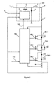
- FIG. 2 schematically depicts a lighting system comprising a control unit 400 arranged to control a switched mode power supply 300 and a LED assembly comprising three LED units 70.1, 70.2 and 70.3.
- the LED assembly further comprises switches (e.g. MOSFET's) 80.1, 80.2 and 80.3 associated with each LED unit for controlling the current per LED unit.
- switches e.g. MOSFET's
- each of the LED units can be driven at a certain duty cycle.
- the control unit 400 is arranged to receive an input signal 110 that may represent a desired characteristic (e.g. a certain brightness or color) of the LED assembly.
- the power supply 300 is known as a buck converter and comprises a switching element 2, an inductance 3 and a diode 4.
- a controller 6 controls the switching of the switching element 2, e.g. based on a reference input 5 and a feedback of the LED assembly.
- a voltage over the resistance 90 of the LED assembly can e.g. be applied as a feedback for the actual current 7 provided by the power supply.
- the control unit 400 can further be arranged to provide an output signal 120 to the power supply 300 for controlling the output of the power supply.
- Designated by reference number 1 is the supply voltage of the power supply (e.g. 16 or 24 V), designated by reference number 8 is the output voltage of the power supply which substantially corresponds to the sum of the voltages over the multiple LED units, also referred to as the forward voltage over the LED units.
- the supply voltage of the power supply e.g. 16 or 24 V
- reference number 8 is the output voltage of the power supply which substantially corresponds to the sum of the voltages over the multiple LED units, also referred to as the forward voltage over the LED units.
- control unit 400 is arranged to provide a control signal to the LED assembly.
- the switches 80 can be controlled and the different LED units can be arranged to operate at a certain duty cycle.
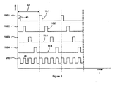
- figure 3 schematically depicts the ON and OFF times for a set of 4 LED units 100.1, 100.2, 100.3 and 100.4 through the curves 10.1, 10.2, 10.3 and 10.4 as a function of time t.
- curve 10.1 could represent the ON time 40 and the OFF time 30-40 for a LED unit 100.1, while the curves 10.2, 10.3 and 10.4 represent the ON and OFF times for units 100.2, 100.3 and 100.4.
- the duty cycle corresponding to curve 10.1 can be expressed as ON time 40 over time 30.
- a current can be provided to the LED unit; during the OFF time, the current can e.g. be redirected to a switch that is in parallel with the LED unit.
- FIG 3 further schematically depicts a curve 20 representing the forward voltage 200 over the serial connection of the 4 LED units. Referring to figure 2 , this forward voltage would substantially correspond to the voltage observed at the output 8 of the power supply 300 (neglecting the voltage over the resistance 90). In the situation as shown, only a single LED unit is switched on at the same time. As such, the forward voltage over the serial connection of the 4 LED units will be moderate, e.g. 3-4 V.
- figure 4 schematically depicts the required duty cycles for the LED units at a reduced current.
- the duty cycles of the LED units may need to increase, e.g. compare the ratio 40/30 in figures 3 and 4 .
- the forward voltage 200 over the LED units can be substantially larger.
- the reduced current substantially corresponds to the nominal current multiplied with the largest duty cycle. By doing so, an adjusted duty cycle of approx. 100 % will be obtained for the LED unit having the largest duty cycle. As the duty cycle of the LED units cannot be more than 100%, the reduced current as obtained in this way corresponds to the smallest current that enables the provision of the desired characteristic of the LED assembly.
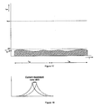
- FIG 5 schematically depicts a brightness (B) characteristic for a LED unit.
- the brightness (B) characteristic shows the brightness (B) as a function of the current through the LED unit. Indicated on the graph is the brightness Bnom corresponding to the nominal current Inom.
- a reduced brightness Br would be obtained when a current I1 is applied in stead of Inom.
- a current I1 will produce a brightness smaller than Br.
- a current I2 is required.
- the largest duty cycle of the LED units (as calculated based on the nominal current) would correspond to Br/Bnom, a current reduction of Inom to I1 would results in a reduced brightness that cannot be compensated entirely by increasing the duty cycle, as this would require a duty cycle above 100%.
- the current can be reduced to I2.
- the control unit according to the present invention can advantageously be applied for controlling a LED assembly comprising two or more LED units that are connected in series.
- the determination of the duty cycles for the multiple LED units using a control unit according to the present invention may result in an improvement of the efficiency of the power supply powering the LED units.
- adjusting the duty cycles of the LED units as described above may result in the application of larger duty cycles in order to compensate for the application of a reduced current.
- the application of a larger duty cycle for a LED unit may have a further advantage in that it may reduce flicker. Flicker of a LED assembly may occur as either visible flicker or non-visible flicker, the latter may e.g. cause nausea.
- a LED unit is e.g. operated at a duty cycle of 90%, a smaller occurring flicker can be observed compared to a duty cycle of e.g. 10%.
- the present invention provides in an improved way of powering a LED assembly comprising a plurality of LED units, arranged in parallel, each LED unit being powered by a different power supply, e.g. a switched mode current supply such as a buck or boost converter.
- a switched mode current supply such as a buck or boost converter.
- the LED assembly to comprise two LED's connected in parallel, each provided with a switched mode current supply for providing a current to the LED.
- the light emitted by the LED's having substantially the same color.
- the conventional way is to adjust the duty cycles of the different LED's in the same manner.
- a desired brightness of 50% of the nominal (or maximal) brightness can be realised by controlling both LED's substantially at a duty cycle of 50%. Note that a correction as discussed in figure 5 may equally be applied.
- the present invention proposed to take the actual efficiency characteristic of the power supplies into account.
- a brightness of 50 % may equally be realised by operating one of the LED's at 100% duty cycle and the other LED at 0% duty cycle.
- the efficiency of the power supply when powering a LED at a 50 % duty cycle may be lower than the efficiency at a 100 % duty cycle, the application of different duty cycles may prove advantageous.
- a control unit can be arranged to determine which combination of duty cycles provide for the best efficiency for a given desired characteristic of the LED assembly.
- An efficiency characteristic of a power supply can e.g. be determined experimentally or based on theoretical considerations.
- Figure 6 depicts a time diagram to illustrate a duty cycling of LEDs according to the state of the art. Time is depicted along the horizontal axis while the LED current as provided by the power supply (e.g. the current provided by the power supply 300 in fig. 1 ) is depicted along the vertical axis.
- the LED current as provided by the power supply e.g. the current provided by the power supply 300 in fig. 1
- a constant, nominal current Inom is sent through the LED during ON time and is obstructed to flow through the LED at OFF time - in the configuration according to fig. 1 e.g. by a closing of the parallel switch, as explained above.
- An average brightness is proportional to surface B1 and B2 respectively as indicated in fig. 6 .
- the average brightness is proportional to the factor t/T.
- t1/T 0.25
- t2/T 1.
- the on time of the LED or LEDs is formed by a single pulse.
- the on time period may be formed by a plurality of shorter time periods, together providing the desired duty cycle.
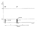
- Figure 7 depicts a time diagram of the LED current versus time, however at a lower duty cycle then in the examples provided by fig.6 , to thereby illustrate a resolution limit in duty cycling according to the state of the art.
- a duty cycle is modulated in a number of steps, e.g. expressed as a 16 bit number.
- a minimum duty cycle step is hence provided by the number of bits and the duty cycle time.
- changing the duty-cycle with the minimal duty cycle step, f.e. from t3 to t4 has a relatively high impact on the average brightness.
- bringing back the duty cycle from t3 to t4 reduces the brightness by a factor A/B3, hence providing, percentagewise, a substantial reduction which may be noticeable to the user as a sudden decrease in brightness.
- Figure 8 depicts a time diagram of the LED current versus time to illustrate how extra room for higher resolutions is achieved by lowering the LED current.
- the same brightnesses (depicted by B3 and B4 in previous figure 7 ) can also be achieved by lowering Inom and increasing the t/T (duty cycle) by a factor which substantially corresponds to the decrease in duty cycle.
- the larger duty cycle at the lower Inom will increase a brightness resolution as the duty cycle can then be altered in smaller steps. Thereby, the brightness may be controlled at a higher resolution with the same duty cycle t3-t4 steps as described above, as the larger duty cycle makes it possible to decrease the duty cycle at a higher resolution.
- the concept of dimming the LEDs by a combination of duty cycle dimming and reducing the power supply current may, depending on the configuration, implementation, dimensioning, and other factors, provide for one of more of the below effects:
- Figure 9 depicts a time diagram of the LED current versus time to again illustrate how the higher resolution in brightness may be achieved by using a smallest duty cycle step in time.
- Figure 10 depicts a time diagram of the LED current versus time to illustrate how the time duty cycle can be applied from 0% to 100% at various values for Inom, thus delivering various brightness steps per duty cycle step. Combined with the logarithmic sensitivity of the human eye, this provides small brightness steps at low brightness.
- Inom using e.g. a 6 to 8 bit potentiometer from a low value at low brightness setpoints to a high value at high brightness setpoints and controlling the brightness in between those points using duty cycling from 0 to 100%
- the brightness can be controlled at a very high resolution of f.e. 20 bit by a combination of e.g. a 16 bit duty cycle and a 4 bit potentiometer.
- Figure 11 depicts a highly conceptual circuit diagram to illustrate a traditional current control.
- the current ILED delivered by the current source provided by in this example a buck converter topology from a supply voltage Vsup, is fed through the LEDs and through the parallel resistances R1, R2 and R3.
- a voltage drop across the R1 through R3 resistance is fed back to the current source at a feedback input FB of the buck converter, thereby enabling control of an amplitude of the current.
- Duty cycle is controlled by the microcontroller ⁇ C, which, in response to a setpoint at a corresponding setpoint input, controls switches, such as In this example switching transistors, connected in parallel to each of the LEDs or LED groups. In order to take account of possible potential differences, the switches are controlled by the microcontroller via respective level converters.
- the current source in this example controls its output current by controlling the voltage present at input FB to a fixed value.
- the total R1 through R3 resistance f.e. by mounting different values for R2 and/or R3 or even leaving them out altogether, different current values can be set that will deliver the same voltage at pin FB.
- the nominal current Inom can be set to different values, e.g. for different applications.
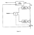
- Figure 12 depicts a highly schematic circuit diagram to illustrate a principle of replacing the above feedback resistance (typically only changeable through soldering) from the previous figure by a potentiometer.
- the potentiometer is connected such as to feed back a part of the voltage across the series resistor Rs to the pin FB.
- the feedback voltage at the FB input is controlled, which provides for a controlling of the value of the LED current I LED .
- the digital potentiometer may be controllable by the microcontroller uC (as indicated by the dotted line) and thus by a suitable software programming and may form an integral part of the brightness and color control algorithm in the microcontroller uC.
- a suitable software programming may form an integral part of the brightness and color control algorithm in the microcontroller uC.
- WO2006107199 A2 Especially the very flexible set of algorithms as described in WO2006107199 A2 . Making use such algorithms, very smooth take-over profiles can be achieved when changing the I nom (and consequently time duty cycle settings).
- the voltage across the (possibly very low ohmic) series resistor Rs is amplified by an amplifier circuit comprising in this example an operational amplifier and potentiometer P2 as a voltage feedback network, and level-shifted by potentiometer D1 connected between an output of the amplifier circuit, a reference voltage (indicated in fig. 13 as 3V3), Consequently, amplification and level-shifting can be set using potentiometers P1 and P2.
- Several op-amp topologies can be used, as will be appreciated by those skilled in the art, to optimise this circuit, for example to achieve an independent level and amplitude control, or to optimise the value of Rs.
- potentiometer P1 use could also be made of a digital to analogue converter, e.g. a multibit converter or a digital duty cycled signal filtered by a low pass filter, in order to provide a microcontroller controlled voltage or current to the feedback circuit.
- a digital to analogue converter e.g. a multibit converter or a digital duty cycled signal filtered by a low pass filter
- a current source is provided per group of LEDs (e.g. per LED unit), each group e.g. providing a different color, so that for each color the current and corresponding duty cycle can be set independently.
- a dimming of one of the colors, and a corresponding change in current will not affect a duty cycle of the other colors, as the current for these colors is independently set.
- each control loop comprises a respective operational amplifier circuit to amplify the voltage across the respective series feedback resistor through which the respective power supply current flows.
- the respective output of the opamp circuit is connected to the respective feedback input FB of the respective converter.
- a voltage amplification factor of the opamp circuits is set by the respective potentiometer setting, in order to set each of the power supply currents.
- a plurality of parallel branches may be provided, each comprising at least one LED unit, a respective switched mode power supply being provided for each of the branches, the control unit being arranged for determining a power supply current for each of the power supplies, depending on the desired output characteristic for the respective LED unit, and for providing output data for each of the power supplies.
- Fig. 15 depicts a time diagram of the LED current versus time to illustrate how even higher resolution may be provided.
- "current duty cycling” is introduced.
- the minimum step has been chosen to be 1 mA on a base setting for the current of 100mA. By having a current of 101 mA during ta and of 100mA during T-ta, the average current is 100.1 when ta is 10% of T.
- the average current can be fine tuned thus providing extra resolution.
- resolution can thus be increased further, adding the resolutions of the time duty cycle of the parallel switches, the current level resolution and the current duty cycle resolution.
- other effects may occur, such as a reduction of flickering, noise and/or electromagnetic interference.
- the additional degree of freedom provided thereby may be applied to optimize efficiency, color display, software complexity (hence required processing power of the microcontroller) or any other suitable parameter such as noise, electromagnetic interference, flickering, etc..
- Fig. 16 which depicts a time diagram of the LED current versus time to illustrate how such mechanism enables achieving high brightness resolutions even when Inom cannot be below a certain threshold dictated by current stability and or color shift. (In a certain range, the color shifting could even be used for fine-tuning the color setting.)
- FIG. 15 it is shown that, given a certain average LED parameter (f.e. Brightness), different settings can be chosen to achieve that average brightness. For example, one could choose the values used in figure 15 (100, 101, 10%) or the values used in this figure (100, 104, 2.5%) to achieve 100.1 mA average current.
- a current profile such as depicted in fig. 16 may also be applied to synchronize with an image capturing rate of a camera.
- Figure 17 depicts a time diagram of the LED current versus time to illustrate effects introduced by a too low power supply current.
- a ripple on the power supply current may occur due to instability of the DC/DC converter.
- LEDs exhibit a behaviour wherein at a too low current, a "knee" in the brightness curve may occur resulting in LED color spectrum shift, unpredictable behaviour or other effects.
- Such a color spectrum shift is illustrated in fig. 18 , schematically depicting a spectral diagram of the LED output spectrum, and showing a first and a shifted second the color spectrum for a different LED current.
- Fig. 19 depicts a time diagram of LED current versus time. This figure illustrates how an average current below the minimum current can be achieved by operating the current source at a current above the minimum current for a first part T4 of the cycle time T, and switching off the current for a second part t of the cycle time T.
- the switching off may be obtained by appropriate setting the Potentiometer ratio (in a suitable feedback circuit configuration) or by closing the parallel switches during a certain part of the duty cycle time.
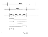
- Fig. 20 depicts a time diagram of LED current versus time.
- the current is set sufficiently large such that the time duty cycle for each color R, G, B and W does not need to be larger than 25%.
- the current algorithm as described previously in WO2006107199 A2 and where each color is primarily controlled in its own time quadrant (i.e. each part) of the cycle time, is greatly simplified, as it is only required to control each color in the quadrant meant for controlling that specific color thereby avoiding cross effects as in each quadrant only the appropriate color and no other color is required to be operational.
- the current can be set to a low value in the cycle time parts corresponding to R, G and B, thereby allowing to drive the respective LEDs at a relatively high time duty cycle within that cycle part, while in the cycle time part corresponding to W, a higher power supply current is set.
- the various embodiments as depicted and described with reference to figs 6 - 20 allow to increase a resolution at lower brightness by altering the current of the power supply, which may be achieved accurately and cost effectively making use of e.g. a digital potentiometer, i.e. a low cost, microprocessor controllable electronic component.
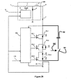
- Fig. 21A depicts a graphical view of the LED current I versus time.
- An example of a circuit to generate this current is depicted in fig. 23 .
- the circuit comprises a switch SW, such as a field effect transistor or other semiconductor switching element in series connection with an inductor IND.
- the current flowing through the inductor then flows through the LED's, e.g. in series connection.
- a resistor Rsens is provided in order to sense a value of the current.
- the current value results in a voltage drop over the resistor Rsens, which is amplified by amplifier AMP and provided to an input of comparator COMP.
- a fly-back diode is provided for allowing current flow when the switch is non conductive.
- the current flows through the resistor Rsens in both the conductive and non conductive state of the switch, or only in the conductive state.
- Another input of the comparator is provided with a reference signal, in this embodiment a reference voltage provided by reference source Vref (also briefly referred to as reference).
- Vref also briefly referred to as reference.
- An output signal of the comparator which represents a result of the comparison, is provided to a controlling input of the switch, in this example to the gate of the field effect transistor.
- a regenerative circuit is provided now, whereby a value of the current through the inductor, LEDs and measurement element averages a value at which the input of the comparator to which the amplifier is connected, equates the value of the reference voltage, thereby the comparator and switch periodically switching, resulting in a ripple on the current as well as on the voltage sensed by the resistor Rsens.
- At least one of the comparator COMP and reference source Vref is controllable by a microcontroller MP.
- the comparator and reference source may be integrated, together with the microprocessor, into a single chip. Hysteresis may be added to the comparator. Therefore, the circuit topology described here sometimes being referred to as a "hysteretical converter" (with hysteresis or without).
- the microprocessor may control the reference source so as to provide different reference voltage values.
- This may for example be implemented by a microprocessor switchable resistive voltage divider network or any other suitable means.
- the reference voltage may be set at a first value during a first part of a cycle time, and at a second value during a second (e.g. remaining) part of the cycle time.
- an effective, average value of the current may be achieved in between the 16 steps, hence enabling a higher resolution dimming.
- a reduction of the current to a lower value during relatively shorter parts of the cycle time may allow precise adjustment of the required average current level.
- the value during the short time period may be set to a desired lower or higher level, or for example to zero, so as to stop the LED current in this part of the cycle.
- instability or other adverse or undesired effects may occur in the circuit as depicted in fig. 23 . Therefore, instead of setting the reference to a continuously low value (for example a value of 1 or 2 in a 4 bit coding), the value may be set somewhat higher, i.e.
- the current may, from the zero current condition, be increased stepwise, e.g. by a stepwise increase of the reference voltage value.
- Fig. 21 D depicts the situation where during a part of the cycle the current is increased for increased resolution of the average current: e.g.
- an increase of the average current may be obtained at a relatively high resolution by setting the current value from 3 to for example 4 during one part of the 64, as schematically depicted in fig. 21D .
- the current may be set by the microcontroller by controlling a value of the reference Vref.
- the condition of zero current may also be achieved by disabling the comparator (e.g. by an internal disabling of a microprocessor controlled comparator or by a switch or digital logic (not depicted in fig. 23 ) that disables of blocks the output of the comparator.
- a current pulse is formed during a part of the cycle time.
- the current pulses may be generated in many ways: it is for example possible to switch the reference Vref from zero to a certain nonzero value, which then results in an increase in the current, while after a certain time (e.g. a lapse of time determined by the microprocessor, a first switching of the comparator and switch SW to the non conductive state of the switch, etc.) the operation is stopped by for example disabling the comparator or setting the value of the reference back to zero, causing the current drop to zero again. Calibration may be performed to determine an effective current value or brightness or brightness contribution of such pulse.
- One pulse may be provided per cycle ( fig 22A ) or a plurality thereof ( fig. 22B ). Although in fig. 22B the pulses are depicted so as to directly follow each other, it will be understood that the pulses may also be provided with a time in between, thereby achieving a further dimming. In an embodiment, dimming may be provided by increasing a time distance between successive pulses.
- an amplitude of the pulse may be set.
- the pulses may provide for a comparatively lower effective current then a continuous current, a resolution may be further increased by combinations of parts of the cycle during which a continuous current is provided, and parts of the cycle during which the current is pulsed.
- different values of the continuous and/or the pulsed current may be obtained within a cycle.
- Calibration of the pulses may be performed in various ways, e.g. timing a pulse width by a timer, filtering a sequence of pulses by a low pass filter, measuring a pulse shape using sub-sampling techniques. Also, feedback mechanisms such as optical feedback (brightness measurement) may be applied.
- asynchronous sampling is used by the microprocessor in order to determine a time of switching off the comparator.
- the microprocessor samples an analogue signal representing the current through the inductor and LED's, e.g. by sampling the signal at the output of the amplifier AMP for amplifying the signal measured by Rsens. Due to the free running character of the hysteretical or other converter, an asynchronous sampling is provided enabling to determine the waveform and hence the switching on and/or off of the comparator with a comparably high resolution. For this purpose, the current may be sampled and/or the output of the comparator.
- the microprocessor may now disable the hysteretical converter (or other type of converter) by either setting after a time (e.g. prior to the finalisation of the cycle of oscillation of the converter itself) the value of the reference source back to zero, by overriding or by disabling the comparator or by any other suitable means to force the switch SW to the desired state.
- a time e.g. prior to the finalisation of the cycle of oscillation of the converter itself
- the comparator or by any other suitable means to force the switch SW to the desired state.
- a frequency of repetition of the pulses may be determined by the microprocessor by the time until a following enabling of the converter (by e.g. a following setting of the reference generator and/or a following enabling of the comparator. Thereby, current pulses may be generated e.g. 1, 2, 3 of N (N being an integer) times per cycle time. Furthermore, it is possible to synchronise the switching of the converter to cycle times of the operation of the microprocessor by the described interaction by the microprocessor on the comparator.
- the above principle may be applied in a method for dimming of the LED current provided by a driver.
- the method comprises:
- figs. 24A - 24C depict the current I of the converter, the reference value Ref and an enable signal E that enables/disables the converter (e.g. by enabling/disabling the comparator), during 3 cycle time parts Tcp.
- fig. 24A free running operation of the converter is enabled until almost the end of the cycle time part Tcp.
- the reference is increased which causes an increase of the current to a higher level, followed by a disabling of the converter by a corresponding level of the enable signal E.
- the same processes are started earlier in the cycle, causing the current of the converter to drop to zero during the final part of each cycle time part Tcp.
- the dimming has progressed further, causing only the increase of the current.
- the reference is set to a high value during at least the part of the cycle time part during which the current increases.
- Further dimming is possible, as explained above, by a reduction of the pulse height and/or time duration (by reducing the value of the reference and/or a reduction of the enable time during which the converter is enabled) of one or more of the pulses of each cycle.
- the dimming may be implemented in the driver by e.g. a corresponding programming of the microprocessor or other microcontroller thereof.
- FIG. 25A- 25C again time diagrams are shown of cycle parts.
- a cycle is formed by 3326 microseconds (providing approximately 300 Hz cycle frequency) and the cycle is divided In 64 cycle parts. It is remarked that other cycle lengths and other divisions of the cycle in cycle time parts, e.g. in 128 cycle time parts, would be possible as well.
- fig. 25C a situation is depicted wherein the switch SW of the converter is activated for a short time, namely in this example 0,125 microseconds by enable signal E that enables the converter. As a result, the current I exhibits a peak each time the comparator is enabled.
- the hysteretical converter would start - at that moment the current would rise again causing a second peak in the same cycle time part, hence an increase in the average current.
- a gradual increase in the time during which the converter is enabled within each cycle would result in a rather stepwise increase in the current, hence in the intensity of the LED's.
- This effect may be at least partly avoided by applying a dithering or other variation to the enable pulse length: instead of a same pulse length in each cycle time part, the length is varied so as to arrive at an average corresponding to the desired cycle time. Therefore, in some of the cycle time parts, the enable time is longer than the average, and in others, the enable time is shorter.
- An example is illustrated in fig. 25A .
- an enable pulse width E of 12 microseconds is applied in the first cycle time part.
- the pulse width is increased in steps of 0.125 microseconds to 20 microseconds.
- the comparator and switch SW are activated slightly more than one cycle of the converter in the first cycle time part, while in the last cycle time part the comparator and switch SW of the converter are activated for slightly more than 2 cycles.
- the above described effect of a stepwise increase will play a role in some of the cycle time parts, while not playing a role in others. Therefore, an averaging takes place, which may result in a more smooth increase of the LED current and intensity with an increase in the average enable time of each cycle.
- a an additional pulse may be added: the microprocessor (microcontroller) may for example start with providing a pulse in one of the cycle time parts of the cycle time, and add a pulse in another one of the cycle time part of the cycle time, for each next higher intensity level.
- the added pulses may be provided in a random one of the cycle time parts of the cycle time.
- they may be provided in a cycle time that is the most distant in time from the already present pulses: for example, in case of 64 cycle time parts in a cycle, and having started with a pulse in cycle part 1, the next pulse can be provided by the microprocessor in cycle part 33, as 33 is most distant from 1 in the same cycle time and from 1 in the next cycle time.
- a user set-point may need a recalculation: for very low intensities, (e.g. the case of fig. 25B and 25C , a small increase in pulse length or in the number of pulses, will result in a comparably larger increase in intensity, then a same increase in the situation in fig.
- the dimming as disclosed here may be described as the controller being arranged to provide enable pulses to enable the comparator in at least two cycle time parts of a cycle time, wherein a pulse length of the enable pulses is varied within each cycle time.
- the variation of the pulse length smoothens a level increase with increased average pulse length, as the effects of parts of the pulses being in "dead times" between successive active times of the hysteretical converter switching cycle, may be smoothened.
- the pulse lengths may be varied applying a linear, Gaussian, random or any other suitable distribution.
- the dimming as described with reference to fig. 25A-C may for example be applied in an LED driver comprising the free running converter as described above, however the application is not limited thereto. Rather, it may be applied in any other converter type too.
- the dimming may be implemented in the driver by e.g. a corresponding programming of the microprocessor MP or other microcontroller thereof.
- the dimming as described with reference to fig. 25A - C may be applied for driving different Led groups, each group e.g. having a different colour, each group being e.g. switchable by means of parallel or serial switches so as to energize or de-energize the group.
- each such group is assigned its own time slot, and the dimming method as described above may then be applied for each of the groups in that specific slot.
- the group is continuously powered in one of the time slots, and the dimming as specified above is applied in another one of the time slots so as to allow accurate and high resolution controlling of the intensity of the respective group.
- a voltage divider to lower a voltage over the LED's to a voltage within a range of measurement of the microprocessor (i.e. the controller).
- this divider may have an effect on the effective current through the LED's, as a part of the current may then flow through the divider instead of through the LED's.
- the value of the resistive divider may have an effect on the decay of the pulse - i.e. the energy stored in the inductor.
- a lower resistance value is chosen for the divider at low current values, to thereby provide a faster decay of the pulses at low current levels.
- a higher resistance value may be chosen (e.g. by suitable switching means under control of the microprocessor) for efficiency reasons.
- FIG. 26 an embodiment of a lighting system according to the present invention is depicted, comprising a control unit 400 arranged to control a switched mode power supply 300 and an LED assembly comprising three LED units 70.1, 70.2 and 70.3.
- the LED assembly further comprises switches (e.g. MOSFET's) 80.1, 80.2 and 80.3 associated with each LED unit for controlling the current per LED unit.
- switches e.g. MOSFET's
- each of the LED units can be driven at a certain duty cycle.
- the LED assembly of the lighting system further comprises a capacitor 82 connectable in parallel to the LED units by closing a switch 84 which is connected in series with the capacitor.
- the application of the capacitor in parallel to the LED units enables to mitigate a current ripple occurring on the current supplied to the LED units since the capacitor operates as a buffer.
- the capacitor is preferably switched on, whereas the capacitor is preferably switched off at comparatively low current levels.
- the switch 84 e.g. a MOSFET or the like
- the operating state of the switch is controlled (by the control unit 400) based upon the operating conditions or power requirements of the LED units.
- the preferred operating state of the switch can e.g. be determined from the input signal 110 (which can e.g.
- the operating state of the switch can be based on the duty cycles applied and/or the current supplied to the LED units.
- the current as required for powering the LED units can be determined by the control unit 400 based on the input signal 110.
- the control unit 400 can provide a control signal to the power supply 300 (e.g. via an output port of the control unit) to control the power supply to provide the desired current.
- the control unit can provide a control signal 86 (e.g. via the same output port) to control the switch 84.
- a comparatively low power output is desired (e.g. dimming light conditions)
- the capacitor 82 and switch 84 are connected in parallel to the LED units 70.1, 70.2 and 70.3 only and not in parallel to the resistance 90 of the LED assembly which can e.g. be applied as a feedback for the actual current 7 provided by the power supply.
- Such an arrangement has been found to provide a preferred current ripple reduction.
- other configurations of the capacitor 82 and switch 84 in parallel to the LED units e.g. a configuration whereby the capacitor 82 and switch 84 as shown are connected to ground, i.e. in parallel to the LED units and the resistance 90
- the LED assembly comprises a plurality of LED units 70.1, 70.2 and 70.3.
- each LED unit may be considered to provide each LED unit with a separate capacitor connectable in parallel to the LED unit by operating a switch connected in series with the capacitor.
- a switch connected in series with the capacitor.
- it can be decided to either connect the respective capacitor in parallel or not, e.g. based on the duty cycle the LED unit is operated at.
- control unit 400 can be arranged to apply the current duty cycling control as explained above, see e.g. Figures 15 and 16 .
- the switch 84 can e.g. be controlled based on either the first or the second value or both.
- the capacitor can be switched on or off during the entire cycle time. If there is a large difference however, it may be advantage to only connect the capacitor in parallel during that part of the cycle time when the largest current is provided.
- the control of the switch 84 can also be based on the duty cycles of the first and second value of the power supply current as applied.
Claims (7)
- Système d'éclairage comprenant :- un ensemble de DEL (70) qui comprend une première (70.1) et une deuxième (70.2) unité de DEL, lesdites unités de DEL étant connectées en série, et ayant chacune un commutateur pour une mise en court-circuit en parallèle ;- une alimentation à mode commuté (300) pour alimenter l'ensemble de DEL ;- une unité de commande (400) pour commander l'ensemble de DEL, l'unité de commande étant agencée pour :et dans lequel l'ensemble de DEL comprend en outre un condensateur (82) pouvant être connecté en parallèle aux première et deuxième unités de DEL en actionnant un commutateur (84) connecté en série avec le condensateur, et dans lequel l'unité de commande est agencée pour commander le commutateur sur la base d'au moins l'un du courant réduit et du signal d'entrée.. recevoir un signal d'entrée (110) représentant une caractéristique de sortie souhaitée de l'ensemble de DEL,. déterminer un premier et un deuxième rapport cyclique pour les première et deuxième unités de DEL respectives associés à un courant nominal de l'alimentation à mode commuté, pour fournir la caractéristique de sortie souhaitée,. déterminer le plus grand des premier et deuxième rapports cycliques pour les unités de DEL respectives,. déterminer un courant réduit pour l'alimentation à mode commuté sur la base au moins du plus grand des rapports cycliques,. ajuster le premier et le deuxième rapport cyclique pour les unités de DEL respectives sur la base du courant réduit ou du plus grand des rapports cycliques,. fournir des données de sortie pour l'ensemble de DEL et l'alimentation à mode commuté sur la base des premier et deuxième rapports cycliques ajustés et du courant réduit,
- Système d'éclairage selon la revendication 1, dans lequel le courant réduit correspond sensiblement au courant nominal multiplié par le rapport cyclique le plus grand.
- Système d'éclairage selon la revendication 1 ou 2, dans lequel le courant réduit est basé sur une caractéristique de luminosité de l'unité de DEL.
- Système d'éclairage selon l'une quelconque des revendications précédentes, dans lequel l'unité de commande comprend un port d'entrée pour recevoir le signal d'entrée.
- Système d'éclairage selon l'une quelconque des revendications précédentes, dans lequel l'unité de commande comprend un port de sortie pour fournir les données de sortie à l'ensemble de DEL et à l'alimentation à mode commuté.
- Système d'éclairage selon la revendication 5, dans lequel l'unité de commande est agencée pour commander le commutateur en fournissant un signal de commande au commutateur par l'intermédiaire du port de sortie.
- Système d'éclairage selon l'une quelconque des revendications précédentes, dans lequel l'unité de commande est agencée pour commander le commutateur sur la base des premier et/ou deuxième rapports cycliques pour les unités de DEL respectives.
Priority Applications (1)
| Application Number | Priority Date | Filing Date | Title |
|---|---|---|---|
| EP14175242.8A EP2836054B1 (fr) | 2009-08-18 | 2010-08-17 | Unité de commande pour un ensemble de diodes électroluminescentes et système d'éclairage |
Applications Claiming Priority (3)
| Application Number | Priority Date | Filing Date | Title |
|---|---|---|---|
| US23479009P | 2009-08-18 | 2009-08-18 | |
| PCT/NL2010/000065 WO2010128845A2 (fr) | 2009-05-04 | 2010-04-09 | Unité de commande pour un ensemble del et un système d'éclairage |
| PCT/NL2010/050516 WO2011021932A1 (fr) | 2009-08-18 | 2010-08-17 | Unité de commande pour ensemble de del et système d'éclairage |
Related Child Applications (1)
| Application Number | Title | Priority Date | Filing Date |
|---|---|---|---|
| EP14175242.8A Division EP2836054B1 (fr) | 2009-08-18 | 2010-08-17 | Unité de commande pour un ensemble de diodes électroluminescentes et système d'éclairage |
Publications (2)
| Publication Number | Publication Date |
|---|---|
| EP2468071A1 EP2468071A1 (fr) | 2012-06-27 |
| EP2468071B1 true EP2468071B1 (fr) | 2014-07-02 |
Family
ID=43037803
Family Applications (2)
| Application Number | Title | Priority Date | Filing Date |
|---|---|---|---|
| EP14175242.8A Active EP2836054B1 (fr) | 2009-08-18 | 2010-08-17 | Unité de commande pour un ensemble de diodes électroluminescentes et système d'éclairage |
| EP10745681.6A Active EP2468071B1 (fr) | 2009-08-18 | 2010-08-17 | Unité de commande pour ensemble de del et système d'éclairage |
Family Applications Before (1)
| Application Number | Title | Priority Date | Filing Date |
|---|---|---|---|
| EP14175242.8A Active EP2836054B1 (fr) | 2009-08-18 | 2010-08-17 | Unité de commande pour un ensemble de diodes électroluminescentes et système d'éclairage |
Country Status (3)
| Country | Link |
|---|---|
| US (1) | US9351365B2 (fr) |
| EP (2) | EP2836054B1 (fr) |
| WO (1) | WO2011021932A1 (fr) |
Families Citing this family (47)
| Publication number | Priority date | Publication date | Assignee | Title |
|---|---|---|---|---|
| TWI459858B (zh) | 2008-06-24 | 2014-11-01 | Eldolab Holding Bv | 照明系統及發光二極體組件之控制單元 |
| US9300113B2 (en) * | 2009-06-18 | 2016-03-29 | Versatile Power, Inc. | Apparatus and method for driving multiple lasers |
| US8531127B2 (en) * | 2010-02-24 | 2013-09-10 | Cal Poly Pomona Foundation, Inc | Computer controlled power supply assembly for a LED array |
| US9482397B2 (en) | 2010-03-17 | 2016-11-01 | Once Innovations, Inc. | Light sources adapted to spectral sensitivity of diurnal avians and humans |
| DE102010003136A1 (de) * | 2010-03-23 | 2011-09-29 | Osram Gesellschaft mit beschränkter Haftung | Schaltungsanordnung und Verfahren zum Betreiben mindestens einer LED |
| US8939604B2 (en) | 2011-03-25 | 2015-01-27 | Arkalumen Inc. | Modular LED strip lighting apparatus |
| EP2533612A1 (fr) * | 2011-06-10 | 2012-12-12 | Exscitron GmbH | Dispositif d'alimentation pour DEL en mode de contrôle non activé |
| US9060400B2 (en) | 2011-07-12 | 2015-06-16 | Arkalumen Inc. | Control apparatus incorporating a voltage converter for controlling lighting apparatus |
| TWI450473B (zh) * | 2011-08-18 | 2014-08-21 | Qisda Corp | 控制對待充能電子裝置之充電電流強度的電子裝置 |
| US8773038B2 (en) * | 2011-08-26 | 2014-07-08 | Infineon Technologies Ag | Driver circuit for efficiently driving a large number of LEDs |
| EP2749128B1 (fr) | 2011-10-20 | 2015-01-28 | Koninklijke Philips N.V. | Circuit d'attaque pour la connexion de diode électroluminescente à un ballast électronique |
| ITPD20120025A1 (it) * | 2012-02-01 | 2013-08-02 | Automotive Lighting Italia S P A A Socio Unico | Circuito di pilotaggio di led, metodo di pilotaggio e fanale automobilistico |
| US20130229124A1 (en) * | 2012-03-05 | 2013-09-05 | Luxera, Inc. | Dimmable Solid State Lighting System, Apparatus, and Article Of Manufacture Having Encoded Operational Parameters |
| JP5602781B2 (ja) * | 2012-03-30 | 2014-10-08 | 株式会社 ヘイワ | Led素子の駆動方法及び駆動用電源装置 |
| CN104396343A (zh) * | 2012-06-25 | 2015-03-04 | 欧司朗股份有限公司 | 照明模块的电流需求控制 |
| JP5988207B2 (ja) * | 2012-09-07 | 2016-09-07 | パナソニックIpマネジメント株式会社 | 固体発光素子駆動装置及び照明装置、照明器具 |
| US8957589B2 (en) * | 2012-11-21 | 2015-02-17 | Shenzhen China Star Optoelectronics Technology Co., Ltd | LED light-adjustment driver module, backlight module and liquid crystal display device |
| WO2014085837A2 (fr) * | 2012-12-06 | 2014-06-12 | Tridonic Gmbh & Co Kg | Appareil de commande d'un moyen d'éclairage |
| US11140879B2 (en) * | 2012-12-11 | 2021-10-12 | Signify North America Corporation | Methods for controlling sex of oviparous embryos using light sources |
| US20140265885A1 (en) * | 2013-03-12 | 2014-09-18 | Cree, Inc. | Multiple power outputs generated from a single current source |
| EP2833699A1 (fr) | 2013-07-29 | 2015-02-04 | ELMOS Semiconductor AG | Dispositif d'alimentation de, et réduction de pointes de courant/tension en, diodes électroluminescentes |
| CN109600884B (zh) | 2013-08-02 | 2021-02-12 | 昕诺飞北美公司 | 对家畜进行照明的系统和方法 |
| CN107911906B (zh) | 2013-09-11 | 2019-12-03 | 万斯创新公司 | Dc led无驱动照明组件 |
| DE102013223710A1 (de) * | 2013-11-20 | 2015-05-21 | Osram Gmbh | Steuern eines wenigstens zwei Halbleiterlichtquellen aufweisenden Leuchtmittels |
| CN104853474A (zh) * | 2013-12-24 | 2015-08-19 | 理察·蓝德立·葛瑞 | 直接式发光二极体驱动装置 |
| US9247603B2 (en) | 2014-02-11 | 2016-01-26 | Once Innovations, Inc. | Shunt regulator for spectral shift controlled light source |
| US20160088702A1 (en) * | 2014-09-24 | 2016-03-24 | Richard Landry Gray | Devices for LED Direct Driver |
| JP6641080B2 (ja) * | 2014-11-05 | 2020-02-05 | ローム株式会社 | 発光素子駆動装置、発光装置、車両 |
| US9510409B2 (en) | 2015-02-19 | 2016-11-29 | Semisilicon Technology Corp. | Light emitting diode driving system with light signals carried via power lines |
| US9380662B1 (en) * | 2015-02-19 | 2016-06-28 | Semisilicon Technology Corp. | Light emitting diode driving system with lighting signals carried via power lines |
| US10225904B2 (en) * | 2015-05-05 | 2019-03-05 | Arkalumen, Inc. | Method and apparatus for controlling a lighting module based on a constant current level from a power source |
| US9992829B2 (en) * | 2015-05-05 | 2018-06-05 | Arkalumen Inc. | Control apparatus and system for coupling a lighting module to a constant current DC driver |
| US9992836B2 (en) * | 2015-05-05 | 2018-06-05 | Arkawmen Inc. | Method, system and apparatus for activating a lighting module using a buffer load module |
| US10568180B2 (en) * | 2015-05-05 | 2020-02-18 | Arkalumen Inc. | Method and apparatus for controlling a lighting module having a plurality of LED groups |
| AT516860B1 (de) * | 2015-06-01 | 2016-09-15 | Zizala Lichtsysteme Gmbh | LED-Lichtmodul für eine Beleuchtungseinrichtung für Fahrzeuge |
| US10451226B2 (en) | 2015-09-14 | 2019-10-22 | ProPhotonix Limited | Modular LED line light |
| EP3145277B1 (fr) * | 2015-09-17 | 2020-11-11 | Nxp B.V. | Circuits, systèmes et procédés de commande de circuits ou chaînes de del |
| EP3437437B1 (fr) | 2016-03-29 | 2023-07-26 | Signify North America Corporation | Système et procédé d'éclairage de bétail |
| US10348974B2 (en) * | 2016-08-02 | 2019-07-09 | Cree, Inc. | Solid state lighting fixtures and image capture systems |
| JP6775189B2 (ja) * | 2016-08-30 | 2020-10-28 | パナソニックIpマネジメント株式会社 | 点灯装置及び車両 |
| US10314125B2 (en) | 2016-09-30 | 2019-06-04 | Once Innovations, Inc. | Dimmable analog AC circuit |
| KR102599600B1 (ko) * | 2016-11-23 | 2023-11-07 | 삼성전자주식회사 | 디스플레이 장치 및 그 구동 방법 |
| DE102017204907A1 (de) * | 2017-03-23 | 2018-09-27 | Osram Gmbh | Verfahren und getakteter Wandler zum Betreiben von einer Eingangsleistung schnell folgenden Lichtquellen |
| JP2019035925A (ja) * | 2017-08-22 | 2019-03-07 | 株式会社Joled | 輝度制御装置、発光装置および輝度制御方法 |
| NL2019587B1 (en) | 2017-09-20 | 2019-03-28 | Eldolab Holding Bv | LED driver and method |
| CN110798939A (zh) * | 2019-11-11 | 2020-02-14 | 杰华特微电子(张家港)有限公司 | Led驱动电路及方法 |
| IT202000023632A1 (it) | 2020-10-07 | 2022-04-07 | Zaglio S R L | Unità e metodo di alimentazione per dispositivi di illuminazione a led |
Family Cites Families (13)
| Publication number | Priority date | Publication date | Assignee | Title |
|---|---|---|---|---|
| US20060038803A1 (en) * | 2004-08-20 | 2006-02-23 | Semiconductor Components Industries, Llc | LED control method and structure therefor |
| CA2768198C (fr) | 2005-04-08 | 2013-11-26 | Eldolab Holding B.V. | Procedes et appareils d'exploitation de groupes de del a haute puissance |
| US20080241455A1 (en) | 2005-07-22 | 2008-10-02 | Dinello Panfilo M | Encapsulated Members, and Processes and Apparatuses for Forming Same |
| US8791645B2 (en) | 2006-02-10 | 2014-07-29 | Honeywell International Inc. | Systems and methods for controlling light sources |
| US20070267241A1 (en) | 2006-05-05 | 2007-11-22 | Textron Inc. | Small utility vehicle frame with prevailing torque weld nuts |
| US7723926B2 (en) * | 2006-05-15 | 2010-05-25 | Supertex, Inc. | Shunting type PWM dimming circuit for individually controlling brightness of series connected LEDS operated at constant current and method therefor |
| US8067896B2 (en) | 2006-05-22 | 2011-11-29 | Exclara, Inc. | Digitally controlled current regulator for high power solid state lighting |
| US7671575B1 (en) * | 2006-11-07 | 2010-03-02 | National Semiconductor Corporation | Transient load response for a voltage regulator with a load current based control loop |
| US7902771B2 (en) | 2006-11-21 | 2011-03-08 | Exclara, Inc. | Time division modulation with average current regulation for independent control of arrays of light emitting diodes |
| CN101779522B (zh) * | 2007-07-23 | 2014-11-19 | Nxp股份有限公司 | 具有旁路驱动的led装置 |
| CN102318440B (zh) | 2007-08-24 | 2015-09-09 | 塞瑞斯逻辑公司 | 多led控制 |
| EP2311297B1 (fr) * | 2008-07-09 | 2018-09-26 | Nxp B.V. | Convertisseur de puissance à découpage et son procédé de fonctionnement |
| WO2010005291A1 (fr) * | 2008-07-11 | 2010-01-14 | Eldolab Holding B.V. | Convertisseur d'énergie pour un ensemble led et application d'éclairage |
-
2010
- 2010-08-17 US US13/390,581 patent/US9351365B2/en active Active
- 2010-08-17 EP EP14175242.8A patent/EP2836054B1/fr active Active
- 2010-08-17 EP EP10745681.6A patent/EP2468071B1/fr active Active
- 2010-08-17 WO PCT/NL2010/050516 patent/WO2011021932A1/fr active Application Filing
Also Published As
| Publication number | Publication date |
|---|---|
| WO2011021932A1 (fr) | 2011-02-24 |
| US20120223649A1 (en) | 2012-09-06 |
| EP2836054B1 (fr) | 2020-10-14 |
| EP2836054A1 (fr) | 2015-02-11 |
| US9351365B2 (en) | 2016-05-24 |
| EP2468071A1 (fr) | 2012-06-27 |
Similar Documents
| Publication | Publication Date | Title |
|---|---|---|
| US10390398B2 (en) | Control unit for a LED assembly and lighting system | |
| EP2468071B1 (fr) | Unité de commande pour ensemble de del et système d'éclairage | |
| US10045408B2 (en) | Control unit for a LED assembly and lighting system | |
| US8334659B2 (en) | Electronic driver dimming control using ramped pulsed modulation for large area solid-state OLEDs | |
| US9386653B2 (en) | Circuits and methods for driving light sources | |
| US8680787B2 (en) | Load control device for a light-emitting diode light source | |
| US9232591B2 (en) | Circuits and methods for driving light sources | |
| US10485063B2 (en) | Power supply circuit, and related lighting system and method for operating a power supply circuit | |
| EP2958401B1 (fr) | Circuit de commande de DEL et procédé associé à une commande de DEL |
Legal Events
| Date | Code | Title | Description |
|---|---|---|---|
| PUAI | Public reference made under article 153(3) epc to a published international application that has entered the european phase |
Free format text: ORIGINAL CODE: 0009012 |
|
| 17P | Request for examination filed |
Effective date: 20120227 |
|
| AK | Designated contracting states |
Kind code of ref document: A1 Designated state(s): AL AT BE BG CH CY CZ DE DK EE ES FI FR GB GR HR HU IE IS IT LI LT LU LV MC MK MT NL NO PL PT RO SE SI SK SM TR |
|
| DAX | Request for extension of the european patent (deleted) | ||
| GRAP | Despatch of communication of intention to grant a patent |
Free format text: ORIGINAL CODE: EPIDOSNIGR1 |
|
| RIN1 | Information on inventor provided before grant (corrected) |
Inventor name: WELTEN, PETRUS, JOHANNES, MARIA Inventor name: SAES, MARC |
|
| GRAS | Grant fee paid |
Free format text: ORIGINAL CODE: EPIDOSNIGR3 |
|
| GRAP | Despatch of communication of intention to grant a patent |
Free format text: ORIGINAL CODE: EPIDOSNIGR1 |
|
| INTG | Intention to grant announced |
Effective date: 20140305 |
|
| GRAA | (expected) grant |
Free format text: ORIGINAL CODE: 0009210 |
|
| AK | Designated contracting states |
Kind code of ref document: B1 Designated state(s): AL AT BE BG CH CY CZ DE DK EE ES FI FR GB GR HR HU IE IS IT LI LT LU LV MC MK MT NL NO PL PT RO SE SI SK SM TR |
|
| REG | Reference to a national code |
Ref country code: GB Ref legal event code: FG4D |
|
| REG | Reference to a national code |
Ref country code: CH Ref legal event code: EP |
|
| REG | Reference to a national code |
Ref country code: IE Ref legal event code: FG4D |
|
| REG | Reference to a national code |
Ref country code: DE Ref legal event code: R096 Ref document number: 602010017234 Country of ref document: DE Effective date: 20140814 |
|
| REG | Reference to a national code |
Ref country code: NL Ref legal event code: T3 |
|
| REG | Reference to a national code |
Ref country code: LT Ref legal event code: MG4D |
|
| REG | Reference to a national code |
Ref country code: AT Ref legal event code: REF Ref document number: 703736 Country of ref document: AT Kind code of ref document: T Effective date: 20150115 |
|
| PG25 | Lapsed in a contracting state [announced via postgrant information from national office to epo] |
Ref country code: LT Free format text: LAPSE BECAUSE OF FAILURE TO SUBMIT A TRANSLATION OF THE DESCRIPTION OR TO PAY THE FEE WITHIN THE PRESCRIBED TIME-LIMIT Effective date: 20140702 Ref country code: BG Free format text: LAPSE BECAUSE OF FAILURE TO SUBMIT A TRANSLATION OF THE DESCRIPTION OR TO PAY THE FEE WITHIN THE PRESCRIBED TIME-LIMIT Effective date: 20141002 Ref country code: SE Free format text: LAPSE BECAUSE OF FAILURE TO SUBMIT A TRANSLATION OF THE DESCRIPTION OR TO PAY THE FEE WITHIN THE PRESCRIBED TIME-LIMIT Effective date: 20140702 Ref country code: ES Free format text: LAPSE BECAUSE OF FAILURE TO SUBMIT A TRANSLATION OF THE DESCRIPTION OR TO PAY THE FEE WITHIN THE PRESCRIBED TIME-LIMIT Effective date: 20140702 Ref country code: PT Free format text: LAPSE BECAUSE OF FAILURE TO SUBMIT A TRANSLATION OF THE DESCRIPTION OR TO PAY THE FEE WITHIN THE PRESCRIBED TIME-LIMIT Effective date: 20141103 Ref country code: GR Free format text: LAPSE BECAUSE OF FAILURE TO SUBMIT A TRANSLATION OF THE DESCRIPTION OR TO PAY THE FEE WITHIN THE PRESCRIBED TIME-LIMIT Effective date: 20141003 Ref country code: CZ Free format text: LAPSE BECAUSE OF FAILURE TO SUBMIT A TRANSLATION OF THE DESCRIPTION OR TO PAY THE FEE WITHIN THE PRESCRIBED TIME-LIMIT Effective date: 20140702 Ref country code: FI Free format text: LAPSE BECAUSE OF FAILURE TO SUBMIT A TRANSLATION OF THE DESCRIPTION OR TO PAY THE FEE WITHIN THE PRESCRIBED TIME-LIMIT Effective date: 20140702 Ref country code: NO Free format text: LAPSE BECAUSE OF FAILURE TO SUBMIT A TRANSLATION OF THE DESCRIPTION OR TO PAY THE FEE WITHIN THE PRESCRIBED TIME-LIMIT Effective date: 20141002 |
|
| PG25 | Lapsed in a contracting state [announced via postgrant information from national office to epo] |
Ref country code: LV Free format text: LAPSE BECAUSE OF FAILURE TO SUBMIT A TRANSLATION OF THE DESCRIPTION OR TO PAY THE FEE WITHIN THE PRESCRIBED TIME-LIMIT Effective date: 20140702 Ref country code: PL Free format text: LAPSE BECAUSE OF FAILURE TO SUBMIT A TRANSLATION OF THE DESCRIPTION OR TO PAY THE FEE WITHIN THE PRESCRIBED TIME-LIMIT Effective date: 20140702 Ref country code: HR Free format text: LAPSE BECAUSE OF FAILURE TO SUBMIT A TRANSLATION OF THE DESCRIPTION OR TO PAY THE FEE WITHIN THE PRESCRIBED TIME-LIMIT Effective date: 20140702 Ref country code: CY Free format text: LAPSE BECAUSE OF FAILURE TO SUBMIT A TRANSLATION OF THE DESCRIPTION OR TO PAY THE FEE WITHIN THE PRESCRIBED TIME-LIMIT Effective date: 20140702 Ref country code: IS Free format text: LAPSE BECAUSE OF FAILURE TO SUBMIT A TRANSLATION OF THE DESCRIPTION OR TO PAY THE FEE WITHIN THE PRESCRIBED TIME-LIMIT Effective date: 20141102 |
|
| REG | Reference to a national code |
Ref country code: AT Ref legal event code: MK05 Ref document number: 703736 Country of ref document: AT Kind code of ref document: T Effective date: 20140702 |
|
| REG | Reference to a national code |
Ref country code: CH Ref legal event code: PL |
|
| REG | Reference to a national code |
Ref country code: DE Ref legal event code: R097 Ref document number: 602010017234 Country of ref document: DE |
|
| PG25 | Lapsed in a contracting state [announced via postgrant information from national office to epo] |
Ref country code: RO Free format text: LAPSE BECAUSE OF FAILURE TO SUBMIT A TRANSLATION OF THE DESCRIPTION OR TO PAY THE FEE WITHIN THE PRESCRIBED TIME-LIMIT Effective date: 20140702 Ref country code: IT Free format text: LAPSE BECAUSE OF FAILURE TO SUBMIT A TRANSLATION OF THE DESCRIPTION OR TO PAY THE FEE WITHIN THE PRESCRIBED TIME-LIMIT Effective date: 20140702 Ref country code: LI Free format text: LAPSE BECAUSE OF NON-PAYMENT OF DUE FEES Effective date: 20140831 Ref country code: BE Free format text: LAPSE BECAUSE OF NON-PAYMENT OF DUE FEES Effective date: 20140831 Ref country code: SK Free format text: LAPSE BECAUSE OF FAILURE TO SUBMIT A TRANSLATION OF THE DESCRIPTION OR TO PAY THE FEE WITHIN THE PRESCRIBED TIME-LIMIT Effective date: 20140702 Ref country code: EE Free format text: LAPSE BECAUSE OF FAILURE TO SUBMIT A TRANSLATION OF THE DESCRIPTION OR TO PAY THE FEE WITHIN THE PRESCRIBED TIME-LIMIT Effective date: 20140702 Ref country code: MC Free format text: LAPSE BECAUSE OF FAILURE TO SUBMIT A TRANSLATION OF THE DESCRIPTION OR TO PAY THE FEE WITHIN THE PRESCRIBED TIME-LIMIT Effective date: 20140702 Ref country code: CH Free format text: LAPSE BECAUSE OF NON-PAYMENT OF DUE FEES Effective date: 20140831 Ref country code: DK Free format text: LAPSE BECAUSE OF FAILURE TO SUBMIT A TRANSLATION OF THE DESCRIPTION OR TO PAY THE FEE WITHIN THE PRESCRIBED TIME-LIMIT Effective date: 20140702 |
|
| PLBE | No opposition filed within time limit |
Free format text: ORIGINAL CODE: 0009261 |
|
| STAA | Information on the status of an ep patent application or granted ep patent |
Free format text: STATUS: NO OPPOSITION FILED WITHIN TIME LIMIT |
|
| REG | Reference to a national code |
Ref country code: IE Ref legal event code: MM4A |
|
| PG25 | Lapsed in a contracting state [announced via postgrant information from national office to epo] |
Ref country code: AT Free format text: LAPSE BECAUSE OF FAILURE TO SUBMIT A TRANSLATION OF THE DESCRIPTION OR TO PAY THE FEE WITHIN THE PRESCRIBED TIME-LIMIT Effective date: 20140702 |
|
| 26N | No opposition filed |
Effective date: 20150407 |
|
| PG25 | Lapsed in a contracting state [announced via postgrant information from national office to epo] |
Ref country code: IE Free format text: LAPSE BECAUSE OF NON-PAYMENT OF DUE FEES Effective date: 20140817 |
|
| PG25 | Lapsed in a contracting state [announced via postgrant information from national office to epo] |
Ref country code: SI Free format text: LAPSE BECAUSE OF FAILURE TO SUBMIT A TRANSLATION OF THE DESCRIPTION OR TO PAY THE FEE WITHIN THE PRESCRIBED TIME-LIMIT Effective date: 20140702 |
|
| PG25 | Lapsed in a contracting state [announced via postgrant information from national office to epo] |
Ref country code: SM Free format text: LAPSE BECAUSE OF FAILURE TO SUBMIT A TRANSLATION OF THE DESCRIPTION OR TO PAY THE FEE WITHIN THE PRESCRIBED TIME-LIMIT Effective date: 20140702 |
|
| PG25 | Lapsed in a contracting state [announced via postgrant information from national office to epo] |
Ref country code: MT Free format text: LAPSE BECAUSE OF FAILURE TO SUBMIT A TRANSLATION OF THE DESCRIPTION OR TO PAY THE FEE WITHIN THE PRESCRIBED TIME-LIMIT Effective date: 20140702 |
|
| PG25 | Lapsed in a contracting state [announced via postgrant information from national office to epo] |
Ref country code: HU Free format text: LAPSE BECAUSE OF FAILURE TO SUBMIT A TRANSLATION OF THE DESCRIPTION OR TO PAY THE FEE WITHIN THE PRESCRIBED TIME-LIMIT; INVALID AB INITIO Effective date: 20100817 Ref country code: TR Free format text: LAPSE BECAUSE OF FAILURE TO SUBMIT A TRANSLATION OF THE DESCRIPTION OR TO PAY THE FEE WITHIN THE PRESCRIBED TIME-LIMIT Effective date: 20140702 Ref country code: BE Free format text: LAPSE BECAUSE OF FAILURE TO SUBMIT A TRANSLATION OF THE DESCRIPTION OR TO PAY THE FEE WITHIN THE PRESCRIBED TIME-LIMIT Effective date: 20140702 Ref country code: LU Free format text: LAPSE BECAUSE OF NON-PAYMENT OF DUE FEES Effective date: 20140817 |
|
| REG | Reference to a national code |
Ref country code: FR Ref legal event code: PLFP Year of fee payment: 7 |
|
| REG | Reference to a national code |
Ref country code: FR Ref legal event code: PLFP Year of fee payment: 8 |
|
| PG25 | Lapsed in a contracting state [announced via postgrant information from national office to epo] |
Ref country code: MK Free format text: LAPSE BECAUSE OF FAILURE TO SUBMIT A TRANSLATION OF THE DESCRIPTION OR TO PAY THE FEE WITHIN THE PRESCRIBED TIME-LIMIT Effective date: 20140702 |
|
| REG | Reference to a national code |
Ref country code: FR Ref legal event code: PLFP Year of fee payment: 9 |
|
| PG25 | Lapsed in a contracting state [announced via postgrant information from national office to epo] |
Ref country code: AL Free format text: LAPSE BECAUSE OF FAILURE TO SUBMIT A TRANSLATION OF THE DESCRIPTION OR TO PAY THE FEE WITHIN THE PRESCRIBED TIME-LIMIT Effective date: 20140702 |
|
| REG | Reference to a national code |
Ref country code: DE Ref legal event code: R079 Ref document number: 602010017234 Country of ref document: DE Free format text: PREVIOUS MAIN CLASS: H05B0033080000 Ipc: H05B0045000000 |
|
| PGFP | Annual fee paid to national office [announced via postgrant information from national office to epo] |
Ref country code: NL Payment date: 20230825 Year of fee payment: 14 |
|
| PGFP | Annual fee paid to national office [announced via postgrant information from national office to epo] |
Ref country code: GB Payment date: 20230824 Year of fee payment: 14 |
|
| PGFP | Annual fee paid to national office [announced via postgrant information from national office to epo] |
Ref country code: FR Payment date: 20230822 Year of fee payment: 14 Ref country code: DE Payment date: 20230822 Year of fee payment: 14 |