EP2461361A2 - Package substrate unit and method for manufacturing package substrate unit - Google Patents
Package substrate unit and method for manufacturing package substrate unit Download PDFInfo
- Publication number
- EP2461361A2 EP2461361A2 EP11153062A EP11153062A EP2461361A2 EP 2461361 A2 EP2461361 A2 EP 2461361A2 EP 11153062 A EP11153062 A EP 11153062A EP 11153062 A EP11153062 A EP 11153062A EP 2461361 A2 EP2461361 A2 EP 2461361A2
- Authority
- EP
- European Patent Office
- Prior art keywords
- layer
- solder
- package substrate
- semiconductor chip
- substrate unit
- Prior art date
- Legal status (The legal status is an assumption and is not a legal conclusion. Google has not performed a legal analysis and makes no representation as to the accuracy of the status listed.)
- Withdrawn
Links
Images






Classifications
-
- H—ELECTRICITY
- H05—ELECTRIC TECHNIQUES NOT OTHERWISE PROVIDED FOR
- H05K—PRINTED CIRCUITS; CASINGS OR CONSTRUCTIONAL DETAILS OF ELECTRIC APPARATUS; MANUFACTURE OF ASSEMBLAGES OF ELECTRICAL COMPONENTS
- H05K3/00—Apparatus or processes for manufacturing printed circuits
- H05K3/46—Manufacturing multilayer circuits
-
- H—ELECTRICITY
- H05—ELECTRIC TECHNIQUES NOT OTHERWISE PROVIDED FOR
- H05K—PRINTED CIRCUITS; CASINGS OR CONSTRUCTIONAL DETAILS OF ELECTRIC APPARATUS; MANUFACTURE OF ASSEMBLAGES OF ELECTRICAL COMPONENTS
- H05K3/00—Apparatus or processes for manufacturing printed circuits
- H05K3/10—Apparatus or processes for manufacturing printed circuits in which conductive material is applied to the insulating support in such a manner as to form the desired conductive pattern
- H05K3/107—Apparatus or processes for manufacturing printed circuits in which conductive material is applied to the insulating support in such a manner as to form the desired conductive pattern by filling grooves in the support with conductive material
-
- B—PERFORMING OPERATIONS; TRANSPORTING
- B23—MACHINE TOOLS; METAL-WORKING NOT OTHERWISE PROVIDED FOR
- B23K—SOLDERING OR UNSOLDERING; WELDING; CLADDING OR PLATING BY SOLDERING OR WELDING; CUTTING BY APPLYING HEAT LOCALLY, e.g. FLAME CUTTING; WORKING BY LASER BEAM
- B23K1/00—Soldering, e.g. brazing, or unsoldering
- B23K1/0008—Soldering, e.g. brazing, or unsoldering specially adapted for particular articles or work
- B23K1/0016—Soldering of electronic components
-
- B—PERFORMING OPERATIONS; TRANSPORTING
- B23—MACHINE TOOLS; METAL-WORKING NOT OTHERWISE PROVIDED FOR
- B23K—SOLDERING OR UNSOLDERING; WELDING; CLADDING OR PLATING BY SOLDERING OR WELDING; CUTTING BY APPLYING HEAT LOCALLY, e.g. FLAME CUTTING; WORKING BY LASER BEAM
- B23K3/00—Tools, devices or special appurtenances for soldering, e.g. brazing, or unsoldering, not specially adapted for particular methods
- B23K3/06—Solder feeding devices; Solder melting pans
- B23K3/0607—Solder feeding devices
- B23K3/0623—Solder feeding devices for shaped solder piece feeding, e.g. preforms, bumps, balls, pellets, droplets
-
- H—ELECTRICITY
- H05—ELECTRIC TECHNIQUES NOT OTHERWISE PROVIDED FOR
- H05K—PRINTED CIRCUITS; CASINGS OR CONSTRUCTIONAL DETAILS OF ELECTRIC APPARATUS; MANUFACTURE OF ASSEMBLAGES OF ELECTRICAL COMPONENTS
- H05K3/00—Apparatus or processes for manufacturing printed circuits
- H05K3/30—Assembling printed circuits with electric components, e.g. with resistors
- H05K3/32—Assembling printed circuits with electric components, e.g. with resistors electrically connecting electric components or wires to printed circuits
- H05K3/34—Assembling printed circuits with electric components, e.g. with resistors electrically connecting electric components or wires to printed circuits by soldering
-
- H—ELECTRICITY
- H10—SEMICONDUCTOR DEVICES; ELECTRIC SOLID-STATE DEVICES NOT OTHERWISE PROVIDED FOR
- H10W—GENERIC PACKAGES, INTERCONNECTIONS, CONNECTORS OR OTHER CONSTRUCTIONAL DETAILS OF DEVICES COVERED BY CLASS H10
- H10W70/00—Package substrates; Interposers; Redistribution layers [RDL]
- H10W70/60—Insulating or insulated package substrates; Interposers; Redistribution layers
- H10W70/67—Insulating or insulated package substrates; Interposers; Redistribution layers characterised by their insulating layers or insulating parts
- H10W70/68—Shapes or dispositions thereof
- H10W70/685—Shapes or dispositions thereof comprising multiple insulating layers
-
- H—ELECTRICITY
- H10—SEMICONDUCTOR DEVICES; ELECTRIC SOLID-STATE DEVICES NOT OTHERWISE PROVIDED FOR
- H10W—GENERIC PACKAGES, INTERCONNECTIONS, CONNECTORS OR OTHER CONSTRUCTIONAL DETAILS OF DEVICES COVERED BY CLASS H10
- H10W90/00—Package configurations
- H10W90/701—Package configurations characterised by the relative positions of pads or connectors relative to package parts
-
- B—PERFORMING OPERATIONS; TRANSPORTING
- B23—MACHINE TOOLS; METAL-WORKING NOT OTHERWISE PROVIDED FOR
- B23K—SOLDERING OR UNSOLDERING; WELDING; CLADDING OR PLATING BY SOLDERING OR WELDING; CUTTING BY APPLYING HEAT LOCALLY, e.g. FLAME CUTTING; WORKING BY LASER BEAM
- B23K2101/00—Articles made by soldering, welding or cutting
- B23K2101/36—Electric or electronic devices
- B23K2101/42—Printed circuits
-
- H—ELECTRICITY
- H10—SEMICONDUCTOR DEVICES; ELECTRIC SOLID-STATE DEVICES NOT OTHERWISE PROVIDED FOR
- H10W—GENERIC PACKAGES, INTERCONNECTIONS, CONNECTORS OR OTHER CONSTRUCTIONAL DETAILS OF DEVICES COVERED BY CLASS H10
- H10W72/00—Interconnections or connectors in packages
- H10W72/071—Connecting or disconnecting
- H10W72/072—Connecting or disconnecting of bump connectors
-
- H—ELECTRICITY
- H10—SEMICONDUCTOR DEVICES; ELECTRIC SOLID-STATE DEVICES NOT OTHERWISE PROVIDED FOR
- H10W—GENERIC PACKAGES, INTERCONNECTIONS, CONNECTORS OR OTHER CONSTRUCTIONAL DETAILS OF DEVICES COVERED BY CLASS H10
- H10W72/00—Interconnections or connectors in packages
- H10W72/20—Bump connectors, e.g. solder bumps or copper pillars; Dummy bumps; Thermal bumps
- H10W72/241—Dispositions, e.g. layouts
-
- H—ELECTRICITY
- H10—SEMICONDUCTOR DEVICES; ELECTRIC SOLID-STATE DEVICES NOT OTHERWISE PROVIDED FOR
- H10W—GENERIC PACKAGES, INTERCONNECTIONS, CONNECTORS OR OTHER CONSTRUCTIONAL DETAILS OF DEVICES COVERED BY CLASS H10
- H10W72/00—Interconnections or connectors in packages
- H10W72/20—Bump connectors, e.g. solder bumps or copper pillars; Dummy bumps; Thermal bumps
- H10W72/281—Auxiliary members
- H10W72/283—Reinforcing structures, e.g. bump collars
-
- H—ELECTRICITY
- H10—SEMICONDUCTOR DEVICES; ELECTRIC SOLID-STATE DEVICES NOT OTHERWISE PROVIDED FOR
- H10W—GENERIC PACKAGES, INTERCONNECTIONS, CONNECTORS OR OTHER CONSTRUCTIONAL DETAILS OF DEVICES COVERED BY CLASS H10
- H10W90/00—Package configurations
- H10W90/701—Package configurations characterised by the relative positions of pads or connectors relative to package parts
- H10W90/721—Package configurations characterised by the relative positions of pads or connectors relative to package parts of bump connectors
- H10W90/724—Package configurations characterised by the relative positions of pads or connectors relative to package parts of bump connectors between a chip and a stacked insulating package substrate, interposer or RDL
-
- Y—GENERAL TAGGING OF NEW TECHNOLOGICAL DEVELOPMENTS; GENERAL TAGGING OF CROSS-SECTIONAL TECHNOLOGIES SPANNING OVER SEVERAL SECTIONS OF THE IPC; TECHNICAL SUBJECTS COVERED BY FORMER USPC CROSS-REFERENCE ART COLLECTIONS [XRACs] AND DIGESTS
- Y10—TECHNICAL SUBJECTS COVERED BY FORMER USPC
- Y10T—TECHNICAL SUBJECTS COVERED BY FORMER US CLASSIFICATION
- Y10T29/00—Metal working
- Y10T29/49—Method of mechanical manufacture
- Y10T29/49002—Electrical device making
- Y10T29/49117—Conductor or circuit manufacturing
- Y10T29/49124—On flat or curved insulated base, e.g., printed circuit, etc.
- Y10T29/49155—Manufacturing circuit on or in base
- Y10T29/49165—Manufacturing circuit on or in base by forming conductive walled aperture in base
Definitions
- the embodiments discussed herein are directed to a package substrate unit and a method for manufacturing the package substrate unit.
- a buildup substrate that includes interstitial vias (IVHs) formed in a core layer for establishing an electrical connection between specific layers, IVH pads formed on the core layer, vias formed in a buildup layer, via pads formed on the buildup layer, and wiring patterns.
- IVHs interstitial vias
- Such a multilayer buildup substrate is also known to function as a package substrate unit.
- FIG. 19 is an exemplary configuration of a conventional package substrate unit 100 having a multilayer structure.
- FIG. 19 is a configuration diagram of the conventional package substrate unit 100.
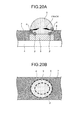
- FIG. 20A is a cross-sectional view of a conventional semiconductor chip mounting layer.
- FIG. 20B is a plan view of the conventional semiconductor chip mounting layer.
- the package substrate unit 100 includes a semiconductor chip mounting layer 3, a ball grid array (BGA) solder ball mounting layer 19, an insulation layer 4 ( FIG. 20A ), and an insulation layer 5. Besides, it is formed to have a multilayer buildup structure that includes insulation layers 14 functioning as topside and underside buildup layers respectively and each having vias 12 and via pads 13, a core layer 15, and solder resist layers 7 and 16.
- BGA ball grid array
- through holes 17 are formed at predetermined positions.
- a through hole via 18 with a pair of the via pads 13 lying above and below.
- a semiconductor chip 10 is mounted as an electronic component on the top surface of the semiconductor chip mounting layer 3.
- the semiconductor chip mounting layer 3 includes the insulation layer 4 ( FIG. 20A ), conductive pads 6 and the solder resist layer 7 that are formed on the top surface of the insulation layer 4. On the solder resist layer 7, openings 8 that are located at the upper side are formed at predetermined positions ( FIG. 19 ). Solder bumps 11 that are formed at the end terminals of the semiconductor chip 10 form solder joints with solder bumps 9 that are formed at the openings 8, which are formed on the solder resist layer 7 of the semiconductor chip mounting layer 3.
- eutectic solder (Sn/Pb) is used in the solder bumps 9.
- a package substrate has been disclosed in which copper posts and copper bumps functioning as electroplating electrodes for forming solder joints with the copper posts are provided in solder bumps that are formed on a base resin layer on which an electronic component such as a semiconductor chip is mounted.
- Patent Literature 1 Japanese Laid-open Patent Publication No. 2008-42118
- lead-free solders have a higher melting-point temperature (for example, 220°C) than the melting-point temperature (for example, 183°C) of eutectic solders.
- the difference in thermal expansion at the time of mounting the semiconductor chip 10 in the package substrate unit 100 causes lead-free solders to be prone to strain.
- the lead-free solders since the lead-free solders have a higher degree of hardness than eutectic solders, the lead-free solders are more prone to cracks than the eutectic solders.
- the stress on each solder bump 9 is generated at the interfaces between different materials. More particularly, the stress occurs at the interfaces (indicated by black circles ⁇ in the figure) between the solder bumps 9 and the respective openings 8 on the solder resist layer 7 and occurs at the interfaces (indicated by black circles P in the figure) between the conductive pads 6 and the respective solder bumps 9.
- the substrate cannot be configured to be a high density substrate.
- a package substrate unit includes an insulation layer; and an electrode unit that is formed on the insulation layer to establish an electrical joint, via a solder, with an end terminal of an electronic component positioned opposite to the insulation layer, wherein the electrode unit has a protrusion that protrudes toward the electronic component.
- FIG. 1 is a cross-sectional view of a package substrate unit according to a first embodiment.
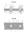
- FIG. 2A is a cross-sectional view of a semiconductor chip mounting layer according to the first embodiment.
- FIG. 2B is a plan view of the semiconductor chip mounting layer according to the first embodiment.
- FIG. 3 is an explanatory diagram for explaining exemplary dimensions of the constituent elements of the semiconductor chip mounting layer.
- a buildup structure is configured from two buildup layers.
- the buildup structure with more than two layers, which include a semiconductor chip mounting layer 20 having metal posts 24 formed thereon according to the first embodiment.
- the semiconductor chip 10 is mounted on the top surface of a package substrate unit 1.
- the package substrate unit 1 includes the semiconductor chip mounting layer 20, a BGA solder ball mounting layer 54, topside buildup layers 30 with vias 31 and via pads 32 formed thereon, a core layer 40, and underside buildup layers 50 with vias 51 and via pads 52 formed thereon.
- the core layer 40 On the core layer 40, through holes 41 are formed at predetermined positions. In each through hole 41 is placed a through hole via 43 with a pair of via pads 42 lying above and below. Besides, wirings 42a are formed on the core layer 40.
- the semiconductor chip mounting layer 20 is formed that includes an insulation layer 21 and the BGA solder ball mounting layer 54 is formed that includes an insulation layer 55.
- the package substrate unit 1 is configured to have a multilayer structure by establishing electrical connections between the vias 31 as well as the via pads 32 formed on the topside buildup layers 30, the core layer 40, and the via pads 42 as well as the through hole vias 43 formed on the core layer 40, and by establishing electrical connections between the vias 51 as well as the via pads 52 formed on the underside buildup layers 50, the core layer 40, and the via pads 42 as well as the through hole vias 43 formed on the core layer 40.
- the semiconductor chip 10 is mounted as an electronic component on the top surface of the semiconductor chip mounting layer 20.
- the semiconductor chip mounting layer 20 includes the insulation layer 21, includes a conductive seed metal layer 22a that is formed on the top surface of the insulation layer 2a and around the vias 31, includes conductive pads 23 that are formed on the top surface of the conductive seed metal layer 22a, and includes the metal posts 24 that are formed at the substantially central portion of the top surface of the conductive pads 23.
- the semiconductor chip mounting layer 20 includes a solder resist layer 25 that is formed to surround the conductive pads 23 and the metal posts 24. On the solder resist layer 25, openings 26 that is located at the upper side are formed at predetermined positions (at two positions in FIGS. 2A and 2B ).
- the metal posts 24 that are formed on the top surface of the respective conductive pads 23 become exposed as well as the solder bumps 27 ( FIG. 1 ) that form solder joints with the solder bumps 11 ( FIG. 1 ), which are formed at the end terminals of the semiconductor chip 10 ( FIG. 1 ).
- the conductive seed metal layer 22a lies between the insulation layer 21 and the bottom surface of the solder resist layer 25 as well as the bottom surfaces of the conductive pads 23.
- the conductive seed metal layer 22a is formed with the aim of enhancing the electrical conductivity for the conductive pads 23 and the metal posts 24, enhancing the contact with the insulation layer 21, and enhancing the connection reliability.
- the conductive pads 23 are formed as round shaped pad members and are made of the same material (for example, copper) as the material of the metal posts 24 formed on the top surface of the conductive pads 23. Moreover, the conductive pads 23 along with the respective metal posts 24 function as electrode units for establishing electrical connections with the end terminals of the semiconductor chip 10. Meanwhile, the conductive pads 23 are also known as controlled collapse chip connection (C4) pads.
- C4 pads controlled collapse chip connection
- Each metal post 24 is made of copper material and is formed as a columnar post having upward orientation at the substantially central portion of the corresponding conductive pad 23. Specifically, each metal post 24 is formed at the position at which the corresponding opening 26 is formed on the solder resist layer 25 and at which it supports from inside the height of the solder bump 27 formed at the same opening 26. Thus, the solder bumps 27 are printed around the respective openings 26 formed on the solder resist layer 25 as well as printed around the respective metal posts 24.
- a mounting height T ( FIG. 1 ) between the semiconductor chip 10 and the package substrate unit 1 can be maintained at a predetermined height.
- the mounting height T between the semiconductor chip 10 and the package substrate unit 1 can be maintained at a predetermined height by having the metal posts inside the solder bumps. That makes it possible to prevent the occurrence of strain in the solder bumps 27.
- the metal post 24 is formed in order to support from inside the height of that solder bump 27, the solder amount of the solder bump 27 can be reduced equivalent to the volume of the corresponding metal post 24.
- the pitch P between the conductive pads 23 pitch P 1 > pitch P. Consequently, narrowing of the pitch enables achieving the high density solder bumps.
- the metal posts 24 are formed to be columnar in shape for the purpose of increasing the effect of stress dispersion.
- FIG. 3 illustrates exemplary dimensions of the constituent elements of the semiconductor chip mounting layer 20. Specifically, in FIG. 3 are illustrated a diameter dimension "a" of each metal post 24, a diameter dimension "b” of each conductive pad 23, and a diameter dimension "c” of the solder resist layer 25. Besides, FIG. 3 illustrates a height dimension L 1 of each metal post 24, a height dimension "d” of each solder bump 27, a height dimension L 2 of the solder resist layer 25, and the pitch P between the conductive pads 23. Meanwhile, the numerical values illustrated in FIG. 3 represent the ratio when each opening 26 formed on the solder resist layer 25 is suggested to have the diameter dimension of "1".
- each metal post 24 is a columnar post having the diameter dimension "a” in the range of 0.5 to 0.7.
- Each conductive pad 23 has the diameter dimension "b” in the range of 1.3 to 1.5.
- Each opening 26 formed on the solder resist layer 25 has the diameter dimension "c” equal to 1.0.
- each metal post 24 has the height dimension L 1 in the range of 0.3 to 0.7.
- Each solder bump 27 has the height dimension "d” in the range of 0.1 to 0.83.
- the solder resist layer 25 has the height dimension L 2 in the range of 0.2 to 0.33. Consequently, each metal post 24 gets exposed at positions higher than the solder resist layer 25. Meanwhile, the pitch P between the conductive pads 23 is in the range of 2 to 1.3.
- the height dimension L 1 of the metal posts 24 is configured to be higher than the height dimension L 2 of the solder resist layer 25 (height dimension L 1 > height dimension L 2 )
- each metal post 24 is disposed inside the corresponding solder bump 27 for the purpose of supporting that solder bump 27, it becomes possible to disperse the stress occurring inside that solder bump 27.
- FIG. 4A is a cross-sectional view for explaining the stress distribution acting on a solder bump.
- FIG. 4B is a plan view for explaining the stress distribution acting on a solder bump.
- the stress is generated at the interfaces between the solder bumps 27 and other different materials. Specifically, the stress occurs at the interfaces (indicated by black circle ⁇ in the figure) between the solder bumps 27 and the respective openings 26 on the solder resist layer 25 and occurs at the interfaces (indicated by black circle P in the figure) between the solder bumps 27 and the respective conductive pads 23.
- the stress since the metal posts 24 are formed at the substantially central portion inside the respective solder bumps 27, the stress also occurs at the interfaces (indicated by black circle ⁇ in the figure) between the solder bumps 27 and the respective metal posts 24.
- the stress occurring in the solder bumps 27 in addition to the interfaces between the solder bumps 27 and the respective openings 26 formed on the solder resist layer 25 where the stress occurs conventionally, the stress is also generated at the interfaces (indicated by black circle ⁇ in the figure) between the solder bumps 27 and the respective metal posts 24.
- the stress gets dispersed such a way that the amount of stress focusing on a single location decreases.
- the metal posts 24 facilitate an increase in the number of stressful locations so that the cracks that essentially occur due to the strain by the stress can be prevented from occurring.
- FIG. 5 is a table for explaining a reliability test regarding the solder bumps 27 with the respective metal posts 24.
- the reliability result regarding the solder bumps 27 as illustrated in FIG. 5 depends on the ratio of the height dimension L 2 of the solder resist layer 25 ( FIG. 3 ) and the height dimension L 1 of the metal posts 24.
- the numerical values ( ⁇ 1, 1.5 to 1.7, 2.1, 2.6, 4.0, and 4.1) used under Condition 1 to Condition 8 represent the ratio with the height dimension of the metal posts 24 where the height dimension of the solder resist layer 25 is suggested as "1".
- the temperature of a thermal cycle test known as TCB is set in the range of -55°C to +125°C. Under all conditions except Condition 1, all of the samples passed TCB 3500 cycles and no cracks were found to have occurred.
- the height dimension L 1 of the metal posts 24 is set to be higher than the height dimension of "1" of the solder resist layer 25 (e.g., Conditions 2 ⁇ 8), all samples passed TCB 3500 cycles.
- the height dimension of the metal post L1 is lower than the height dimension of solder resist layer 25 (e.g., Condition 1), cracks occurred inside the solder bumps 27 after TCB 1000 cycles.
- FIG. 6 is a flow chart for explaining the method for manufacturing the package substrate unit according to the first embodiment.
- a substrate manufacturing system first forms the core layer 40 ( FIG. 1 ) at Step S1. That is, firstly, the through holes vias 43 are formed in the core layer 40 followed by the formation of the via pads 42 and the wirings 42a.
- the topside buildup layers 30 and the underside buildup layers 50 are simultaneously formed as the wiring layers on both sides of the core layer 40 ( FIG. 1 ) at Step S2.
- an insulation layer 30a and an insulation layer 50a are formed that respectively constitute the topside buildup layers 30 and the underside buildup layers 50.
- the vias 31, the via pads 32, and wirings 32a are formed as part of the topside buildup layers 30.
- the vias 51, the via pads 52, and wirings 52a are formed as part of the buildup layers 50 under the core layer 40.
- the operation of forming the vias 31 and 51, forming the via pads 32 and 52, and forming the wirings 32a and 52a is repeated until the necessary number of layers is attained. Meanwhile, except the formation of the insulation layers, the formation of layers at Step S2 is performed for the purpose of establishing electrical connections among the layers. Moreover, the operation at Step S2 results in the formation of a wiring layer as the inside layer between the core layer and the semiconductor chip mounting layer.
- a foundation layer of the semiconductor chip mounting layer 20 ( FIG. 1 ) and a foundation layer of the BGA solder ball mounting layer 54 ( FIG. 1 ) are formed at Step S3.
- the foundation layer of the semiconductor chip mounting layer 20 is formed on the topside of the buildup layers 30 formed at Step S2; while the foundation layer of the BGA solder ball mounting layer 54 is formed on the underside of the buildup layers 50 formed at Step S2.
- the insulation layer 21 and the insulation layer 55 are formed on the patterns of the inside layer.
- a conductive seed metal layer 22 ( FIG. 7A ) is formed.
- the vias 31 and the vias 51 are filled with electrolytic plating.
- the conductive pads 23 are formed, which represent the electrode units for establishing electrical connections with the end terminals of the semiconductor chip 10 at the positions immediately above the vias 31, and the wirings 32a are formed.
- BGA pads 53 are formed, which represent the electrode units at the positions immediately below the vias 51, and the wirings 52a are formed.
- the metal posts 24 are formed on the top surface of the conductive pads 23 at Step S4. As described later, at Step S4, the metal posts 24 are formed on the top surface of the conductive pads 23 for the purpose of supporting from inside the solder bumps 27, which form solder joints with the solder bumps 11 formed on the semiconductor chip 10. That is followed by the formation of the solder resist layer 25 and a solder resist layer 60 at Step S5.
- the solder resist layer 25 is formed for the purpose of forming the openings 26 at which the metal posts 24 are disposed. Specifically, by opening the solder resist layer 25 by means of photolithography and development, the openings 26 are formed thereon. At the same time, the solder resist layer 60 is formed for the purpose of forming openings at which BGA solder balls are mounted.
- Step S6 printing of the solder bumps is carried out at Step S6.
- the solder bumps 27 that are lead-free solders are printed at the openings 26, which formed on the solder resist layer 25, and printed on the top surface of the metal posts 24.
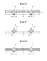
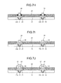
- FIGS. 7A to 7J are explanatory diagrams for explaining the procedure followed while manufacturing the package substrate unit according to the first embodiment. Meanwhile, the manufacturing process of the package substrate unit is performed by implementing a predetermined substrate manufacturing system. The following description is given with reference to the exemplary case of implementing the substrate manufacturing system.
- the conductive seed metal layer 22 is formed by electroless plating before filling the vias 31 with electrolytic plating in the insulation layer 21 constituting the semiconductor chip mounting layer 20 ( FIG. 1 ).
- the conductive seed metal layer 22 is etched out at a latter stage ( FIG. 7F ), it remains intact only at the bottom part of the conductive pads 23 and around the vias 31.
- the conductive seed metal layer 22a remaining at the bottom part of the conductive pads 23 and around the vias 31 becomes a significant connection seed metal layer between the conductive pads 23 and the insulation layer 21 as well as between the vias 31 and the insulation layer 21.
- the conductive seed metal layer 22a makes the conductive pads 23 and the vias 31 stick together with the insulation layer 21.
- vias are formed at predetermined positions on the insulation layer 21 and the surface of the insulation layer 21 is roughened.
- electroless plating is performed to form the conductive seed metal layer 22, which is a metallic plating seed layer, on the surface of the insulation layer 21.
- the conductive seed metal layer 22 is used as the conductive layer and vias 31 are filled up by the electrolytic plating until the via lid plating layer is formed.
- the lid plating layer is patterned to form the conductive pads 23 and the wirings 32a by the photolithographic method. As described above, the conductive pads 23 represent the electrode units for establishing an electrical connection with the semiconductor chip 10.
- a dry film resist layer 34 having a predetermined thickness is formed using a dry film resist on the surface of the copper patterning layer on which the conductive pads 23 have been formed.
- the dry film resist layer 34 is formed in a laminated manner on the semiconductor chip mounting layer 20.
- an photolithography process is performed to expose predetermined regions on the dry film resist layer 34.
- the photolithography of the dry film resist is performed by the photomask so that the patterns for forming the metal posts 24 are transferred on those regions on the dry film resist layer 34 that lie above the top surface of the conductive pads 23.
- the predetermined regions exposed during the photolithography process correspond to the locations at which the metal posts 24 are formed.
- a development process is performed with respect to those predetermined regions on the dry film resist layer 34 that have been exposed during the photolithography process (regions corresponding to post openings).
- openings 35 to be used for forming the metal posts 24 are formed at the predetermined locations on the dry film resist layer 34.
- the openings 35 are columnar in shape.
- plating process is performed with respect to the regions subjected to the development process. More particularly, the metal is electrolytically plated to fill the openings 35 formed as a result of the development process. By filling in the openings 35, the metal posts 24 in columnar shape is formed on the top surface of the conductive pads 23.
- the metal posts 24 in order to form the metal posts 24 on the top surface of the conductive pads 23, a semi-additive method using a dry film resist is implemented.
- the metal posts 24 can also be manufactured by implementing a subtractive method.
- the dry film resist layer 34 formed on the top surface of the insulation layer 21 is stripped off. While stripping off the dry film resist layer 34, as illustrated in FIG. 7F , the conductive seed metal layer 22 is also etched off except that remains under the conductive pads 23. As described above, the conductive seed metal layer 22a remaining at the bottom part of the conductive pads 23 and around the vias 31 becomes a significant connection seed metal layer between the conductive pads 23 and the insulation layer 21 as well as between the vias 31 and the insulation layer 21.
- the solder resist layer 25 is formed to surround the conductive pads 23 and the metal posts 24, which are formed on the top surface of the insulation layer 21.
- the formation position (height dimension L 2 ) of the solder resist layer 25 is set to be lower than the height dimension L 1 of the metal posts 24. That is because, as described above, when the height dimension L 1 of the metal posts 24 is set to be higher than the height dimension L 2 of the solder resist layer 25, the cracks that occur due to the strain caused by the accumulation of the stress can be prevented from occurring inside the solder bumps 27.
- the solder resist layer 25 formed on the top surface of the conductive pads 23 and around the metal posts 24 is exposed using a photomask.
- the development process is performed for the solder printing opening around the metal posts 24. More particularly, the top surface of the conductive pads 23 and the surrounding area of the metal posts 24 are developed.
- the predetermined regions on the solder resist layer 25 that have been developed become the openings 26 at which the solder bumps 27 are printed to form solder joints with the solder bumps 11.
- the solder bumps 27, which are the lead-free solders, are printed around the metal posts 24 located in the center of the openings 26 formed on the solder resist layer 25.
- the package substrate unit 1 can be manufactured in which the metal posts 24 are formed to support from inside the height of the solder bumps 27 that are formed on the semiconductor chip mounting layer 20.
- the conductive seed metal layer 22a is formed on the top surface of the insulation layer 21 and the conductive pads 23 functioning as electrodes are formed on the top surface of the conductive seed metal layer 22a.
- the metal posts 24 that support the height of the solder bumps 27 are formed in the substantially central portion on the top surface of the conductive pads 23. The metal posts 24 enable achieving dispersion of the stress generated inside the solder bumps 27. Therefore, the cracks that essentially occur due to the accumulation of stress can be prevented from occurring inside the solder bumps 27.
- the pitch between the solder bumps 27 can be formed narrower by this metal posts structure and it enables high density solder bumps structure.
- FIG. 8 is a cross-sectional view of a semiconductor chip mounting layer 61 constituting the package substrate unit according to the second embodiment.
- surface treatment with heat resistant pre-flux processing using organic solderability preservatives (OSP) is performed on the surface of the metal posts 24, which are formed on the top surface of the conductive pads 23, and performed on a portion of the top surface of the conductive pads 23 so that a surface treatment layer 81 is formed.
- OSP organic solderability preservatives
- the surface treatment layer 81 on the surface of the metal posts 24 and on a portion of the top surface of the conductive pads 23, it becomes possible to remove the oxide film of the surface of the conductive pads 23 and that of the metal posts 24. Besides, it becomes possible to enhance the connection strength and the electrical conductivity between the surface of the metal posts 24 as well as the surface of the conductive pads 23 and the solder bumps 27 that are formed at the openings 26 on the solder resist layer 25.
- FIG. 9 is a cross-sectional view of a semiconductor chip mounting layer 62 constituting the package substrate unit according to the third embodiment. As illustrated in FIG. 9 , in the semiconductor chip mounting layer 62 according to the third embodiment, openings 26a formed on the solder resist layer 25 are formed to be wider in dimension. Besides, the solder bumps 27, which form solder joints with the solder bumps 11 formed on the semiconductor chip 10, are formed in the shape of mushrooms.
- solder bumps 27 enable achieving enhancement in the electrical conductivity of the solder bumps 27 and the conductive pads 23 with respect to the semiconductor chip 10. Besides, since the solder bumps 27 with the metal posts 24 do not make contact with the openings 26a formed on the solder resist layer 25, the number of contact boundary points decreases. As a result, the cracks that essentially occur due to the stress focusing on the contact points can be prevented from occurring.
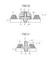
- FIG. 10 is a cross-sectional view of a semiconductor chip mounting layer 63 constituting the package substrate unit according to the fourth embodiment.
- the semiconductor chip mounting layer 63 illustrated in FIG. 10 according to the fourth embodiment differs in the fact that, in addition to the configuration according to the third embodiment, surface treatment with heat resistant pre-flux processing is performed on the surface of the metal posts 24 and on the surface of the conductive pads 23 so that a surface treatment layer 83 is formed. Then, the mushroom-shaped solder bumps 27 are formed on the top surface of the surface treatment layer 83, which is formed on the metal posts 24 and the conductive pads 23.
- the solder bumps 27 enable achieving enhancement in the electrical conductivity of the solder bumps 27 and the conductive pads 23 with respect to the semiconductor chip 10. Moreover, since the surface treatment layer 83 is formed on the metal posts 24 and the conductive pads 23, it becomes possible to enhance the connection strength and the electrical conductivity between the surface of the metal posts 24 as well as the surface of the conductive pads 23 and the solder bumps 27.
- FIG. 11 is a cross-sectional view of a semiconductor chip mounting layer 64 constituting the package substrate unit according to the fifth embodiment.
- the solder bumps 27 are not formed at the openings 26 on the solder resist layer 25.
- solders 84 are formed around the surface of the metal posts 24, which are formed on the top surface of the conductive pads 23.
- the solders 84 are formed only around the surface of the metal posts 24, it becomes possible to reduce the solder amount required for the formation of solder joints between the solder bumps 11, which are formed at the end terminals of the semiconductor chip 10, and the metal posts 24, and this design enables the finer pitch.
- FIG. 12 is a cross-sectional view of a semiconductor chip mounting layer 65 constituting the package substrate unit according to the sixth embodiment.
- surface treatment with heat resistant pre-flux processing is performed on the surface of the metal posts 24 and on a portion of the top surface of the conductive pads 23 so that the surface treatment layer 81 is formed.
- the solders 84 are formed on the surface of the metal posts 24.
- the solder amount can be reduced and the finer pitch is possible in an identical manner to the fifth embodiment.
- the surface treatment layer 81 is formed, it becomes possible to enhance the electrical conductivity of the solder bump 27 and the conductive pads 23 with respect to the semiconductor chip 10.
- FIG. 13 is a cross-sectional view of a semiconductor chip mounting layer 66 constituting the package substrate unit according to the seventh embodiment.
- the openings 26a formed on the solder resist layer 25 are formed to be wider in dimension.
- the solder bumps 27 are not formed at the metal posts 24.
- surface treatment with heat resistant pre-flux processing is performed on the surface of the metal posts 24 and on the surface of the conductive pads 23 so that the surface treatment layer 83 is formed.
- the formation of the surface treatment layer 83 makes it possible to enhance the electrical conductivity of the solder bump 27 and the conductive pads 23 with respect to the semiconductor chip 10.
- FIG. 14 is a cross-sectional view of a semiconductor chip mounting layer 67 constituting the package substrate unit according to the eighth embodiment.
- solder bumps 27a are formed in a small amount on the top surface of the metal posts 24 that are formed on the top surface of the conductive pads 23.
- the solder bumps 27a directly form solder joints with the solder bumps 11 formed on the semiconductor chip 10.
- solder bumps 27a are formed only a small amount on the top surface of the metal posts 24 and the solder bumps 27a directly form solder joints with the solder bumps 11 formed on the semiconductor chip 10, it becomes possible to enhance the electrical conductivity of the metal posts 24 and the conductive pads 23.
- FIG. 15 is a cross-sectional view of a semiconductor chip mounting layer 68 constituting the package substrate unit according to the ninth embodiment.
- metal posts 24a formed on the top surface of the conductive pads 23 are conical in shape with the upper diameter being larger than the lower diameter.
- surface treatment with heat resistant pre-flux processing is performed on the surface of the metal posts 24, which are formed on the top surface of the conductive pads 23, and performed on a portion of the top surface of the conductive pads 23 so that a surface treatment layer 85 is formed.
- a surface treatment layer 85 is formed on the surface of the metal posts 24a and on a portion of the top surface of the conductive pads 23 in the ninth embodiment, it becomes possible to enhance the connection strength and the electrical conductivity between the surface of the metal posts 24a as well as the surface of the conductive pads 23 and the solder bumps 27 that are formed at the openings 26 on the solder resist layer 25.
- the solder bumps 27 are formed at the openings 26 on the solder resist layer 25 and on the surface of the metal posts 24a.
- the solder bumps 27 may not be formed in an identical manner to the seventh embodiment. That is, it is also possible to make the metal posts 24a directly form solder joints with the solder bumps 11 formed on the semiconductor chip 10 via the surface treatment layer 85. In that case, the solder amount can be reduced and this enables the finer pitch structure.
- FIG. 16 is a cross-sectional view of a semiconductor chip mounting layer 69 constituting the package substrate unit according to the tenth embodiment.
- the metal posts 24a formed on the top surface of the conductive pads 23 are conical in shape with the upper diameter being larger than the lower diameter.
- the openings 26a formed on the solder resist layer 25 are formed to be wider in dimension.
- the solder bumps 27, which form solder joints with the solder bumps 11 formed on the semiconductor chip 10 are formed in the shape of mushrooms.
- the solder bumps 27 enable achieving enhancement in the electrical conductivity of the solder bumps 27 and the conductive pads 23 with respect to the semiconductor chip 10.
- FIG. 17 is a cross-sectional view of a semiconductor chip mounting layer 70 constituting the package substrate unit according to the eleventh embodiment.
- metal posts 24b formed on the top surface of the conductive pads 23 are conical in shape with the lower diameter being larger than the upper diameter.
- surface treatment with heat resistant pre-flux processing is performed on the surface of the metal posts 24b, which are formed on the top surface of the conductive pads 23, and performed on a portion of the top surface of the conductive pads 23 so that the surface treatment layer 85 is formed.
- the solder bumps 27 may not be formed and the metal posts 24a may be made to directly form solder joints with the solder bumps 11 formed on the semiconductor chip 10 via the surface treatment layer 85.
- the solder amount can be reduced and the pitch can be made finer.
- FIG. 18 is a cross-sectional view of a semiconductor chip mounting layer 71 constituting the package substrate unit according to the twelfth embodiment.
- the metal posts 24b formed on the top surface of the conductive pads 23 are conical in shape with the lower diameter being larger than the upper diameter.
- the openings 26a formed on the solder resist layer 25 are formed to be wider in dimension.
- the solder bumps 27, which form solder joints with the solder bumps 11 formed on the semiconductor chip 10 are formed in the shape of mushrooms.
Landscapes
- Engineering & Computer Science (AREA)
- Mechanical Engineering (AREA)
- Manufacturing & Machinery (AREA)
- Microelectronics & Electronic Packaging (AREA)
- Wire Bonding (AREA)
- Internal Circuitry In Semiconductor Integrated Circuit Devices (AREA)
Abstract
Description
- The embodiments discussed herein are directed to a package substrate unit and a method for manufacturing the package substrate unit.
- Traditionally, package wiring substrates that are configured to have high density by means of a multilayer structure have been in demand. In that regard, as a wiring substrate configured to have a multilayer and high-density structure, a buildup substrate is known that includes interstitial vias (IVHs) formed in a core layer for establishing an electrical connection between specific layers, IVH pads formed on the core layer, vias formed in a buildup layer, via pads formed on the buildup layer, and wiring patterns. Such a multilayer buildup substrate is also known to function as a package substrate unit.
- Explained below with reference to
FIG. 19 is an exemplary configuration of a conventionalpackage substrate unit 100 having a multilayer structure. Herein,FIG. 19 is a configuration diagram of the conventionalpackage substrate unit 100.FIG. 20A is a cross-sectional view of a conventional semiconductor chip mounting layer.FIG. 20B is a plan view of the conventional semiconductor chip mounting layer. - As illustrated in
FIG. 19 , thepackage substrate unit 100 includes a semiconductorchip mounting layer 3, a ball grid array (BGA) solderball mounting layer 19, an insulation layer 4 (FIG. 20A ), and aninsulation layer 5. Besides, it is formed to have a multilayer buildup structure that includesinsulation layers 14 functioning as topside and underside buildup layers respectively and each havingvias 12 and viapads 13, acore layer 15, andsolder resist layers - In the
core layer 15, throughholes 17 are formed at predetermined positions. In each throughhole 17 is placed a through hole via 18 with a pair of thevia pads 13 lying above and below. Besides, in thepackage substrate unit 100, asemiconductor chip 10 is mounted as an electronic component on the top surface of the semiconductorchip mounting layer 3. - The semiconductor
chip mounting layer 3 includes the insulation layer 4 (FIG. 20A ),conductive pads 6 and thesolder resist layer 7 that are formed on the top surface of theinsulation layer 4. On thesolder resist layer 7,openings 8 that are located at the upper side are formed at predetermined positions (FIG. 19 ).Solder bumps 11 that are formed at the end terminals of thesemiconductor chip 10 form solder joints withsolder bumps 9 that are formed at theopenings 8, which are formed on thesolder resist layer 7 of the semiconductorchip mounting layer 3. Herein, eutectic solder (Sn/Pb) is used in thesolder bumps 9. - Meanwhile, in a publication that discloses a conventional technology, a package substrate has been disclosed in which copper posts and copper bumps functioning as electroplating electrodes for forming solder joints with the copper posts are provided in solder bumps that are formed on a base resin layer on which an electronic component such as a semiconductor chip is mounted.
- Patent Literature 1: Japanese Laid-open Patent Publication No.
2008-42118 - In recent years, from the perspective of environmental measures, there has been a shift from eutectic solders (Sn/Pb) to lead-free solders not containing lead (Pb) (for example, Sn/Ag, Sn/Ag/Cu, Sn/Cu, etc.) as the solders used at the time of mounting semiconductor chips.
- Here, lead-free solders have a higher melting-point temperature (for example, 220°C) than the melting-point temperature (for example, 183°C) of eutectic solders. Hence, the difference in thermal expansion at the time of mounting the
semiconductor chip 10 in the package substrate unit 100 (i.e., during the reflow process) causes lead-free solders to be prone to strain. Besides, since the lead-free solders have a higher degree of hardness than eutectic solders, the lead-free solders are more prone to cracks than the eutectic solders. - Explained below with reference to
FIGS. 20A and 20B are the factors causing cracks in thesolder bumps 9 if lead-free solders are used. Herein, the stress on eachsolder bump 9 is generated at the interfaces between different materials. More particularly, the stress occurs at the interfaces (indicated by black circles α in the figure) between thesolder bumps 9 and therespective openings 8 on thesolder resist layer 7 and occurs at the interfaces (indicated by black circles P in the figure) between theconductive pads 6 and therespective solder bumps 9. - Particularly, since the stress gets concentrated at the interfaces between the
solder bumps 9 and therespective openings 8 on thesolder resist layer 7, cracks occur from the interfaces (indicated by black circles a in the figure) between thesolder bumps 9 and therespective openings 8 on thesolder resist layer 7 toward the central portion of thesolder bumps 9. When such cracks occurs inside thesolder bumps 9, it effects the connection strength between thesolder bumps 9 and therespective solder bumps 11, which are formed at the end terminals of the semiconductor chip 10 (FIG. 19 ). - Meanwhile, in the case of the package substrate disclosed in the conventional technology publication, since the copper posts are formed in the through hole of a base resin layer, the substrate cannot be configured to be a high density substrate. Moreover, in order to form the copper bumps that form solder joints with the copper posts, it is necessary to perform the task of forming openings in the base resin layer by using an expensive laser machine. Besides, it is also necessary to perform the task of uniting or aligning the base resin layer having the copper posts formed thereon with a substrate having solders printed thereon.
- Accordingly, it is desirable to provide a package substrate unit that enables achieving enhancement in the connection reliability between solder bumps formed in an electronic component and solder bumps formed in a package substrate unit.
- According to an aspect of an embodiment of the invention, a package substrate unit includes an insulation layer; and an electrode unit that is formed on the insulation layer to establish an electrical joint, via a solder, with an end terminal of an electronic component positioned opposite to the insulation layer, wherein the electrode unit has a protrusion that protrudes toward the electronic component.
-
-
FIG. 1 is a cross-sectional view of a package substrate unit according to a first embodiment; -
FIG. 2A is a cross-sectional view of a semiconductor chip mounting layer according to the first embodiment; -
FIG. 2B is a plan view of the semiconductor chip mounting layer according to the first embodiment; - FIG. is an explanatory diagram for explaining exemplary dimensions of the constituent elements of the semiconductor chip mounting layer;
-
FIG. 4A is a cross-sectional view for explaining the stress distribution acting on a solder bump; -
FIG. 4B is a plan view for explaining the stress distribution acting on a solder bump; -
FIG. 5 is a diagram for explaining a reliability test regarding solder bumps; -
FIG. 6 is a flow chart for explaining a method for manufacturing the package substrate unit; -
FIGS. 7A to 7J are explanatory diagrams for explaining the method of manufacturing the package substrate unit; -
FIG. 8 is a cross-sectional view of a semiconductor chip mounting layer constituting the package substrate unit according to a second embodiment; -
FIG. 9 is a cross-sectional view of a semiconductor chip mounting layer constituting the package substrate unit according to a third embodiment; -
FIG. 10 is a cross-sectional view of a semiconductor chip mounting layer constituting the package substrate unit according to a fourth embodiment; -
FIG. 11 is a cross-sectional view of a semiconductor chip mounting layer constituting the package substrate unit according to a fifth embodiment; -
FIG. 12 is a cross-sectional view of a semiconductor chip mounting layer constituting the package substrate unit according to a sixth embodiment; -
FIG. 13 is a cross-sectional view of a semiconductor chip mounting layer constituting the package substrate unit according to a seventh embodiment; -
FIG. 14 is a cross-sectional view of a semiconductor chip mounting layer constituting the package substrate unit according to an eighth embodiment; -
FIG. 15 is a cross-sectional view of a semiconductor chip mounting layer constituting the package substrate unit according to a ninth embodiment; -
FIG. 16 is a cross-sectional view of a semiconductor chip mounting layer constituting the package substrate unit according to a tenth embodiment; -
FIG. 17 is a cross-sectional view of a semiconductor chip mounting layer constituting the package substrate unit according to an eleventh embodiment; -
FIG. 18 is a cross-sectional view of a semiconductor chip mounting layer constituting the package substrate unit according to a twelfth embodiment; -
FIG. 19 is a configuration diagram of a conventional package substrate unit; -
FIG. 20A is a cross-sectional view of a conventional semiconductor chip mounting layer; and -
FIG. 20B is a plan view of the conventional semiconductor chip mounting layer. - Preferred embodiments of the present invention will be explained with reference to accompanying drawings.
-
FIG. 1 is a cross-sectional view of a package substrate unit according to a first embodiment.FIG. 2A is a cross-sectional view of a semiconductor chip mounting layer according to the first embodiment.FIG. 2B is a plan view of the semiconductor chip mounting layer according to the first embodiment.FIG. 3 is an explanatory diagram for explaining exemplary dimensions of the constituent elements of the semiconductor chip mounting layer. - Meanwhile, the present invention is not limited to the present embodiment. Besides, in the example illustrated in diagrams, a buildup structure is configured from two buildup layers. However, alternatively, it is also possible to configure the buildup structure with more than two layers, which include a semiconductor
chip mounting layer 20 havingmetal posts 24 formed thereon according to the first embodiment. In the following description according to the first embodiment, it is assumed that thesemiconductor chip 10 is mounted on the top surface of apackage substrate unit 1. - As illustrated in
FIG. 1 , thepackage substrate unit 1 includes the semiconductorchip mounting layer 20, a BGA solderball mounting layer 54, topside buildup layers 30 withvias 31 and viapads 32 formed thereon, acore layer 40, and underside buildup layers 50 withvias 51 and viapads 52 formed thereon. On thecore layer 40, throughholes 41 are formed at predetermined positions. In each throughhole 41 is placed a through hole via 43 with a pair of viapads 42 lying above and below. Besides,wirings 42a are formed on thecore layer 40. - In the
package substrate unit 1, the semiconductorchip mounting layer 20 is formed that includes aninsulation layer 21 and the BGA solderball mounting layer 54 is formed that includes aninsulation layer 55. Thepackage substrate unit 1 is configured to have a multilayer structure by establishing electrical connections between the vias 31 as well as the viapads 32 formed on the topside buildup layers 30, thecore layer 40, and the viapads 42 as well as the throughhole vias 43 formed on thecore layer 40, and by establishing electrical connections between the vias 51 as well as the viapads 52 formed on the underside buildup layers 50, thecore layer 40, and the viapads 42 as well as the throughhole vias 43 formed on thecore layer 40. Besides, thesemiconductor chip 10 is mounted as an electronic component on the top surface of the semiconductorchip mounting layer 20. - As illustrated in
FIGS. 2A and 2B , the semiconductorchip mounting layer 20 includes theinsulation layer 21, includes a conductiveseed metal layer 22a that is formed on the top surface of the insulation layer 2a and around thevias 31, includesconductive pads 23 that are formed on the top surface of the conductiveseed metal layer 22a, and includes the metal posts 24 that are formed at the substantially central portion of the top surface of theconductive pads 23. Besides, the semiconductorchip mounting layer 20 includes a solder resistlayer 25 that is formed to surround theconductive pads 23 and the metal posts 24. On the solder resistlayer 25,openings 26 that is located at the upper side are formed at predetermined positions (at two positions inFIGS. 2A and 2B ). - Moreover, at the formation positions of the
openings 26 on the solder resistlayer 25, the metal posts 24 that are formed on the top surface of the respectiveconductive pads 23 become exposed as well as the solder bumps 27 (FIG. 1 ) that form solder joints with the solder bumps 11 (FIG. 1 ), which are formed at the end terminals of the semiconductor chip 10 (FIG. 1 ). - The conductive
seed metal layer 22a lies between theinsulation layer 21 and the bottom surface of the solder resistlayer 25 as well as the bottom surfaces of theconductive pads 23. Thus, the conductiveseed metal layer 22a is formed with the aim of enhancing the electrical conductivity for theconductive pads 23 and the metal posts 24, enhancing the contact with theinsulation layer 21, and enhancing the connection reliability. - The
conductive pads 23 are formed as round shaped pad members and are made of the same material (for example, copper) as the material of the metal posts 24 formed on the top surface of theconductive pads 23. Moreover, theconductive pads 23 along with therespective metal posts 24 function as electrode units for establishing electrical connections with the end terminals of thesemiconductor chip 10. Meanwhile, theconductive pads 23 are also known as controlled collapse chip connection (C4) pads. - Each
metal post 24 is made of copper material and is formed as a columnar post having upward orientation at the substantially central portion of the correspondingconductive pad 23. Specifically, eachmetal post 24 is formed at the position at which thecorresponding opening 26 is formed on the solder resistlayer 25 and at which it supports from inside the height of thesolder bump 27 formed at thesame opening 26. Thus, the solder bumps 27 are printed around therespective openings 26 formed on the solder resistlayer 25 as well as printed around the respective metal posts 24. - Thus, in the first embodiment, a mounting height T (
FIG. 1 ) between thesemiconductor chip 10 and thepackage substrate unit 1 can be maintained at a predetermined height. Specifically, in thepackage substrate unit 1 according to the first embodiment in which the conductive pads 23 (C4 pads) of finer or narrower pitch, the mounting height T between thesemiconductor chip 10 and thepackage substrate unit 1 can be maintained at a predetermined height by having the metal posts inside the solder bumps. That makes it possible to prevent the occurrence of strain in the solder bumps 27. - Moreover, since, in each
solder bump 27, themetal post 24 is formed in order to support from inside the height of thatsolder bump 27, the solder amount of thesolder bump 27 can be reduced equivalent to the volume of the correspondingmetal post 24. As a result, as compared to the semiconductor chip mounting layer 3 (FIG. 19 ) according to the conventional technology, it is possible to reduce the pitch P between the conductive pads 23 (pitch P1 > pitch P). Consequently, narrowing of the pitch enables achieving the high density solder bumps. - Herein, in the first embodiment, the metal posts 24 are formed to be columnar in shape for the purpose of increasing the effect of stress dispersion. Alternatively, it is also possible to form the metal posts 24 as quadrangular posts, as octagonal posts, as polygonal posts, or as rod-like protrusions.
-
FIG. 3 illustrates exemplary dimensions of the constituent elements of the semiconductorchip mounting layer 20. Specifically, inFIG. 3 are illustrated a diameter dimension "a" of eachmetal post 24, a diameter dimension "b" of eachconductive pad 23, and a diameter dimension "c" of the solder resistlayer 25. Besides,FIG. 3 illustrates a height dimension L1 of eachmetal post 24, a height dimension "d" of eachsolder bump 27, a height dimension L2 of the solder resistlayer 25, and the pitch P between theconductive pads 23. Meanwhile, the numerical values illustrated inFIG. 3 represent the ratio when each opening 26 formed on the solder resistlayer 25 is suggested to have the diameter dimension of "1". - That is, as illustrated in
FIG. 3 , eachmetal post 24 is a columnar post having the diameter dimension "a" in the range of 0.5 to 0.7. Eachconductive pad 23 has the diameter dimension "b" in the range of 1.3 to 1.5. Eachopening 26 formed on the solder resistlayer 25 has the diameter dimension "c" equal to 1.0. Meanwhile, eachmetal post 24 has the height dimension L1 in the range of 0.3 to 0.7. Eachsolder bump 27 has the height dimension "d" in the range of 0.1 to 0.83. The solder resistlayer 25 has the height dimension L2 in the range of 0.2 to 0.33. Consequently, eachmetal post 24 gets exposed at positions higher than the solder resistlayer 25. Meanwhile, the pitch P between theconductive pads 23 is in the range of 2 to 1.3. - In the present embodiment, the height dimension L1 of the metal posts 24 is configured to be higher than the height dimension L2 of the solder resist layer 25 (height dimension L1 > height dimension L2) By having such a configuration, it becomes possible to reliably prevent the occurrence of cracks that are attributed to the focusing or accumulation of stress inside the solder bumps 27.
- In this way, by disposing each
metal post 24 inside thecorresponding solder bump 27 for the purpose of supporting thatsolder bump 27, it becomes possible to disperse the stress occurring inside thatsolder bump 27. - Explained below with reference to
FIGS. 4A and 4B is the stress dispersion effect in which the stress occurring inside the solder bumps 27 gets dispersed with the use of the metal posts 24.FIG. 4A is a cross-sectional view for explaining the stress distribution acting on a solder bump.FIG. 4B is a plan view for explaining the stress distribution acting on a solder bump. - As described above, inside the solder bumps 27, the stress is generated at the interfaces between the solder bumps 27 and other different materials. Specifically, the stress occurs at the interfaces (indicated by black circle α in the figure) between the solder bumps 27 and the
respective openings 26 on the solder resistlayer 25 and occurs at the interfaces (indicated by black circle P in the figure) between the solder bumps 27 and the respectiveconductive pads 23. On the other hand, in the first embodiment, since the metal posts 24 are formed at the substantially central portion inside the respective solder bumps 27, the stress also occurs at the interfaces (indicated by black circle θ in the figure) between the solder bumps 27 and the respective metal posts 24. - Specifically, at the interfaces between the solder bumps 27 and the
respective openings 26 formed on the solder resistlayer 25, there exists a large difference in hardness between the solder resistlayer 25 and the solder bumps 27. Hence, cracks tend to occur by the stress focusing or accumulation at those interfaces. On the other hand, at the interfaces between the solder bumps 27 and therespective metal posts 24, there exists a small difference in hardness between the metal posts 24 and the solder bumps 27. Hence, the stress does not focus or accumulate at those interfaces and there is no occurrence of cracks. - Thus, regarding the stress occurring in the solder bumps 27, in addition to the interfaces between the solder bumps 27 and the
respective openings 26 formed on the solder resistlayer 25 where the stress occurs conventionally, the stress is also generated at the interfaces (indicated by black circle θ in the figure) between the solder bumps 27 and the respective metal posts 24. As a result, the stress gets dispersed such a way that the amount of stress focusing on a single location decreases. Hence, the metal posts 24 facilitate an increase in the number of stressful locations so that the cracks that essentially occur due to the strain by the stress can be prevented from occurring. - Reliability test for solder bumps with metal posts
FIG. 5 is a table for explaining a reliability test regarding the solder bumps 27 with the respective metal posts 24. Herein, the reliability result regarding the solder bumps 27 as illustrated inFIG. 5 depends on the ratio of the height dimension L2 of the solder resist layer 25 (FIG. 3 ) and the height dimension L1 of the metal posts 24. - Herein, 20 samples of the package substrate unit were tested. Moreover, the numerical values (<1, 1.5 to 1.7, 2.1, 2.6, 4.0, and 4.1) used under
Condition 1 toCondition 8 represent the ratio with the height dimension of the metal posts 24 where the height dimension of the solder resistlayer 25 is suggested as "1". Furthermore, the temperature of a thermal cycle test known as TCB is set in the range of -55°C to +125°C. Under all conditions exceptCondition 1, all of the samples passedTCB 3500 cycles and no cracks were found to have occurred. - Specifically, when the height dimension L1 of the metal posts 24 is set to be higher than the height dimension of "1" of the solder resist layer 25 (e.g.,
Conditions 2~8), all samples passedTCB 3500 cycles. In the contrary, when the height dimension of the metal post L1 is lower than the height dimension of solder resist layer 25 (e.g., Condition 1), cracks occurred inside the solder bumps 27 after TCB 1000 cycles. - Under each of
Condition 2 toCondition 8, when the height dimension L1 of the metal posts 24 is set to 1.5 to 1.7, 2.1, 2.6, 4.0, and 4.1, respectively, an evaluation experiment result was obtained in which the occurrence of cracks was not found inside the solder bumps 27 of any of the 20 samples. In this way, when the height dimension L1 of the metal posts 24 is set to be higher than the height dimension L2 of the solder resistlayer 25, the cracks that essentially occur due to the concentration of stress can be prevented from occurring inside the solder bumps 27. - Method for manufacturing package substrate unit
- Explained below with reference to
FIG. 6 is a method for manufacturing the package substrate unit according to the first embodiment. Herein,FIG. 6 is a flow chart for explaining the method for manufacturing the package substrate unit according to the first embodiment. - As illustrated in
FIG. 6 , while manufacturing the package substrate unit, a substrate manufacturing system first forms the core layer 40 (FIG. 1 ) at Step S1. That is, firstly, the through holes vias 43 are formed in thecore layer 40 followed by the formation of the viapads 42 and thewirings 42a. - Subsequently, the topside buildup layers 30 and the underside buildup layers 50 (
FIG. 1 ) are simultaneously formed as the wiring layers on both sides of the core layer 40 (FIG. 1 ) at Step S2. Specifically, on thecore layer 40, aninsulation layer 30a and aninsulation layer 50a are formed that respectively constitute the topside buildup layers 30 and the underside buildup layers 50. Then, thevias 31, the viapads 32, andwirings 32a are formed as part of the topside buildup layers 30. Similarly, thevias 51, the viapads 52, andwirings 52a are formed as part of the buildup layers 50 under thecore layer 40. The operation of forming thevias pads wirings - Subsequently, a foundation layer of the semiconductor chip mounting layer 20 (
FIG. 1 ) and a foundation layer of the BGA solder ball mounting layer 54 (FIG. 1 ) are formed at Step S3. Herein, the foundation layer of the semiconductorchip mounting layer 20 is formed on the topside of the buildup layers 30 formed at Step S2; while the foundation layer of the BGA solderball mounting layer 54 is formed on the underside of the buildup layers 50 formed at Step S2. More particularly, theinsulation layer 21 and theinsulation layer 55 are formed on the patterns of the inside layer. Then, before the formation of thevias 31 and thevias 51 for the purpose of establishing electrical connections, a conductive seed metal layer 22 (FIG. 7A ) is formed. Consequently, thevias 31 and thevias 51 are filled with electrolytic plating. Then, theconductive pads 23 are formed, which represent the electrode units for establishing electrical connections with the end terminals of thesemiconductor chip 10 at the positions immediately above thevias 31, and thewirings 32a are formed. Similarly,BGA pads 53 are formed, which represent the electrode units at the positions immediately below thevias 51, and thewirings 52a are formed. - Subsequently, the metal posts 24 are formed on the top surface of the
conductive pads 23 at Step S4. As described later, at Step S4, the metal posts 24 are formed on the top surface of theconductive pads 23 for the purpose of supporting from inside the solder bumps 27, which form solder joints with the solder bumps 11 formed on thesemiconductor chip 10. That is followed by the formation of the solder resistlayer 25 and a solder resistlayer 60 at Step S5. - At Step S5, the solder resist
layer 25 is formed for the purpose of forming theopenings 26 at which the metal posts 24 are disposed. Specifically, by opening the solder resistlayer 25 by means of photolithography and development, theopenings 26 are formed thereon. At the same time, the solder resistlayer 60 is formed for the purpose of forming openings at which BGA solder balls are mounted. - Subsequently, printing of the solder bumps is carried out at Step S6. At Step S6, the solder bumps 27 that are lead-free solders are printed at the
openings 26, which formed on the solder resistlayer 25, and printed on the top surface of the metal posts 24. - Explained below with reference to
FIGS. 7A to 7J are the details of the manufacturing process of the package substrate unit.FIGS. 7A to 7J are explanatory diagrams for explaining the procedure followed while manufacturing the package substrate unit according to the first embodiment. Meanwhile, the manufacturing process of the package substrate unit is performed by implementing a predetermined substrate manufacturing system. The following description is given with reference to the exemplary case of implementing the substrate manufacturing system. - As illustrated in
FIG. 7A , firstly, the conductiveseed metal layer 22 is formed by electroless plating before filling thevias 31 with electrolytic plating in theinsulation layer 21 constituting the semiconductor chip mounting layer 20 (FIG. 1 ). - Although the conductive
seed metal layer 22 is etched out at a latter stage (FIG. 7F ), it remains intact only at the bottom part of theconductive pads 23 and around thevias 31. As described above, the conductiveseed metal layer 22a remaining at the bottom part of theconductive pads 23 and around thevias 31 becomes a significant connection seed metal layer between theconductive pads 23 and theinsulation layer 21 as well as between the vias 31 and theinsulation layer 21. Thus, the conductiveseed metal layer 22a makes theconductive pads 23 and thevias 31 stick together with theinsulation layer 21. - Specifically, vias are formed at predetermined positions on the
insulation layer 21 and the surface of theinsulation layer 21 is roughened. Subsequently, electroless plating is performed to form the conductiveseed metal layer 22, which is a metallic plating seed layer, on the surface of theinsulation layer 21. The conductiveseed metal layer 22 is used as the conductive layer and vias 31 are filled up by the electrolytic plating until the via lid plating layer is formed. Moreover, the lid plating layer is patterned to form theconductive pads 23 and thewirings 32a by the photolithographic method. As described above, theconductive pads 23 represent the electrode units for establishing an electrical connection with thesemiconductor chip 10. - Subsequently, as illustrated in
FIG. 7B , a dry film resistlayer 34 having a predetermined thickness is formed using a dry film resist on the surface of the copper patterning layer on which theconductive pads 23 have been formed. The dry film resistlayer 34 is formed in a laminated manner on the semiconductorchip mounting layer 20. - Subsequently, as illustrated in
FIG. 7C , an photolithography process is performed to expose predetermined regions on the dry film resistlayer 34. Specifically, the photolithography of the dry film resist is performed by the photomask so that the patterns for forming the metal posts 24 are transferred on those regions on the dry film resistlayer 34 that lie above the top surface of theconductive pads 23. Thus, the predetermined regions exposed during the photolithography process correspond to the locations at which the metal posts 24 are formed. - Subsequently, as illustrated in
FIG. 7D , a development process is performed with respect to those predetermined regions on the dry film resistlayer 34 that have been exposed during the photolithography process (regions corresponding to post openings). As a result of the development process,openings 35 to be used for forming the metal posts 24 are formed at the predetermined locations on the dry film resistlayer 34. As illustrated inFIG. 7D , theopenings 35 are columnar in shape. - Subsequently, as illustrated in
FIG. 7E , plating process is performed with respect to the regions subjected to the development process. More particularly, the metal is electrolytically plated to fill theopenings 35 formed as a result of the development process. By filling in theopenings 35, the metal posts 24 in columnar shape is formed on the top surface of theconductive pads 23. - Meanwhile, in the first embodiment, in order to form the metal posts 24 on the top surface of the
conductive pads 23, a semi-additive method using a dry film resist is implemented. Alternatively, the metal posts 24 can also be manufactured by implementing a subtractive method. - Subsequently, as illustrated in
FIG. 7F , the dry film resistlayer 34 formed on the top surface of theinsulation layer 21 is stripped off. While stripping off the dry film resistlayer 34, as illustrated inFIG. 7F , the conductiveseed metal layer 22 is also etched off except that remains under theconductive pads 23. As described above, the conductiveseed metal layer 22a remaining at the bottom part of theconductive pads 23 and around thevias 31 becomes a significant connection seed metal layer between theconductive pads 23 and theinsulation layer 21 as well as between the vias 31 and theinsulation layer 21. - Subsequently, as illustrated in
FIG. 7G , the solder resistlayer 25 is formed to surround theconductive pads 23 and the metal posts 24, which are formed on the top surface of theinsulation layer 21. In this case, the formation position (height dimension L2) of the solder resistlayer 25 is set to be lower than the height dimension L1 of the metal posts 24. That is because, as described above, when the height dimension L1 of the metal posts 24 is set to be higher than the height dimension L2 of the solder resistlayer 25, the cracks that occur due to the strain caused by the accumulation of the stress can be prevented from occurring inside the solder bumps 27. - Subsequently, as illustrated in
FIG. 7H , the solder resistlayer 25 formed on the top surface of theconductive pads 23 and around the metal posts 24 is exposed using a photomask. Then, as illustrated inFIG. 7I , the development process is performed for the solder printing opening around the metal posts 24. More particularly, the top surface of theconductive pads 23 and the surrounding area of the metal posts 24 are developed. Thus, the predetermined regions on the solder resistlayer 25 that have been developed become theopenings 26 at which the solder bumps 27 are printed to form solder joints with the solder bumps 11. - Subsequently, as illustrated in
FIG. 7J , the solder bumps 27, which are the lead-free solders, are printed around the metal posts 24 located in the center of theopenings 26 formed on the solder resistlayer 25. In this way, according to the sequence explained with reference toFIG. 6 andFIGS. 7A to 7J , thepackage substrate unit 1 can be manufactured in which the metal posts 24 are formed to support from inside the height of the solder bumps 27 that are formed on the semiconductorchip mounting layer 20. - As described above, in the semiconductor
chip mounting layer 20 constituting thepackage substrate unit 1 according to the first embodiment, the conductiveseed metal layer 22a is formed on the top surface of theinsulation layer 21 and theconductive pads 23 functioning as electrodes are formed on the top surface of the conductiveseed metal layer 22a. The metal posts 24 that support the height of the solder bumps 27 are formed in the substantially central portion on the top surface of theconductive pads 23. The metal posts 24 enable achieving dispersion of the stress generated inside the solder bumps 27. Therefore, the cracks that essentially occur due to the accumulation of stress can be prevented from occurring inside the solder bumps 27. - As a result, it becomes possible to secure the connection reliability between the solder bumps 11 formed at the end terminals of the
semiconductor chip 10 and the solder bumps 27 formed on the semiconductorchip mounting layer 20 in thepackage substrate unit 1. Besides, the pitch between the solder bumps 27 can be formed narrower by this metal posts structure and it enables high density solder bumps structure. - Explanations below with reference to
FIGS. 8 to 18 are other examples of a semiconductor chip mounting layer constituting the package substrate units according to second to twelfth embodiments. In the following description of the second to twelfth embodiments, the constituent elements identical to the constituent elements of the semiconductorchip mounting layer 20 according to the first embodiment are referred to by the same reference numerals and the explanation thereof is not repeated. -
FIG. 8 is a cross-sectional view of a semiconductorchip mounting layer 61 constituting the package substrate unit according to the second embodiment. As illustrated inFIG. 8 , in the semiconductorchip mounting layer 61 according to the second embodiment, surface treatment with heat resistant pre-flux processing using organic solderability preservatives (OSP) is performed on the surface of the metal posts 24, which are formed on the top surface of theconductive pads 23, and performed on a portion of the top surface of theconductive pads 23 so that asurface treatment layer 81 is formed. - Thus, in the second embodiment, by forming the
surface treatment layer 81 on the surface of the metal posts 24 and on a portion of the top surface of theconductive pads 23, it becomes possible to remove the oxide film of the surface of theconductive pads 23 and that of the metal posts 24. Besides, it becomes possible to enhance the connection strength and the electrical conductivity between the surface of the metal posts 24 as well as the surface of theconductive pads 23 and the solder bumps 27 that are formed at theopenings 26 on the solder resistlayer 25. -
FIG. 9 is a cross-sectional view of a semiconductorchip mounting layer 62 constituting the package substrate unit according to the third embodiment. As illustrated inFIG. 9 , in the semiconductorchip mounting layer 62 according to the third embodiment,openings 26a formed on the solder resistlayer 25 are formed to be wider in dimension. Besides, the solder bumps 27, which form solder joints with the solder bumps 11 formed on thesemiconductor chip 10, are formed in the shape of mushrooms. - Thus, in the third embodiment, such solder bumps 27 enable achieving enhancement in the electrical conductivity of the solder bumps 27 and the
conductive pads 23 with respect to thesemiconductor chip 10. Besides, since the solder bumps 27 with the metal posts 24 do not make contact with theopenings 26a formed on the solder resistlayer 25, the number of contact boundary points decreases. As a result, the cracks that essentially occur due to the stress focusing on the contact points can be prevented from occurring. -
FIG. 10 is a cross-sectional view of a semiconductorchip mounting layer 63 constituting the package substrate unit according to the fourth embodiment. As compared to the configuration illustrated inFIG. 9 according to the third embodiment, the semiconductorchip mounting layer 63 illustrated inFIG. 10 according to the fourth embodiment differs in the fact that, in addition to the configuration according to the third embodiment, surface treatment with heat resistant pre-flux processing is performed on the surface of the metal posts 24 and on the surface of theconductive pads 23 so that asurface treatment layer 83 is formed. Then, the mushroom-shaped solder bumps 27 are formed on the top surface of thesurface treatment layer 83, which is formed on the metal posts 24 and theconductive pads 23. - Thus, according to the fourth embodiment, in an identical manner to the third embodiment, the solder bumps 27 enable achieving enhancement in the electrical conductivity of the solder bumps 27 and the
conductive pads 23 with respect to thesemiconductor chip 10. Moreover, since thesurface treatment layer 83 is formed on the metal posts 24 and theconductive pads 23, it becomes possible to enhance the connection strength and the electrical conductivity between the surface of the metal posts 24 as well as the surface of theconductive pads 23 and the solder bumps 27. -
FIG. 11 is a cross-sectional view of a semiconductorchip mounting layer 64 constituting the package substrate unit according to the fifth embodiment. As illustrated inFIG. 11 , in the semiconductorchip mounting layer 64 according to the fifth embodiment, the solder bumps 27 are not formed at theopenings 26 on the solder resistlayer 25. Instead, solders 84 are formed around the surface of the metal posts 24, which are formed on the top surface of theconductive pads 23. Thus, in the fifth embodiment, since thesolders 84 are formed only around the surface of the metal posts 24, it becomes possible to reduce the solder amount required for the formation of solder joints between the solder bumps 11, which are formed at the end terminals of thesemiconductor chip 10, and the metal posts 24, and this design enables the finer pitch. -
FIG. 12 is a cross-sectional view of a semiconductorchip mounting layer 65 constituting the package substrate unit according to the sixth embodiment. As illustrated inFIG. 12 , in the semiconductorchip mounting layer 65 according to the sixth embodiment, surface treatment with heat resistant pre-flux processing is performed on the surface of the metal posts 24 and on a portion of the top surface of theconductive pads 23 so that thesurface treatment layer 81 is formed. In addition, thesolders 84 are formed on the surface of the metal posts 24. Thus, in the sixth embodiment, the solder amount can be reduced and the finer pitch is possible in an identical manner to the fifth embodiment. Besides, since thesurface treatment layer 81 is formed, it becomes possible to enhance the electrical conductivity of thesolder bump 27 and theconductive pads 23 with respect to thesemiconductor chip 10. -
FIG. 13 is a cross-sectional view of a semiconductorchip mounting layer 66 constituting the package substrate unit according to the seventh embodiment. As illustrated inFIG. 13 , in the semiconductorchip mounting layer 66 according to the seventh embodiment, theopenings 26a formed on the solder resistlayer 25 are formed to be wider in dimension. Besides, the solder bumps 27 are not formed at the metal posts 24. Moreover, surface treatment with heat resistant pre-flux processing is performed on the surface of the metal posts 24 and on the surface of theconductive pads 23 so that thesurface treatment layer 83 is formed. Thus, in the seventh embodiment, the formation of thesurface treatment layer 83 makes it possible to enhance the electrical conductivity of thesolder bump 27 and theconductive pads 23 with respect to thesemiconductor chip 10. -
FIG. 14 is a cross-sectional view of a semiconductorchip mounting layer 67 constituting the package substrate unit according to the eighth embodiment. As illustrated inFIG. 14 , in the semiconductorchip mounting layer 67 according to the eighth embodiment, solder bumps 27a are formed in a small amount on the top surface of the metal posts 24 that are formed on the top surface of theconductive pads 23. The solder bumps 27a directly form solder joints with the solder bumps 11 formed on thesemiconductor chip 10. - Thus, in the eighth embodiment, since the solder bumps 27a are formed only a small amount on the top surface of the metal posts 24 and the solder bumps 27a directly form solder joints with the solder bumps 11 formed on the
semiconductor chip 10, it becomes possible to enhance the electrical conductivity of the metal posts 24 and theconductive pads 23. -
FIG. 15 is a cross-sectional view of a semiconductorchip mounting layer 68 constituting the package substrate unit according to the ninth embodiment. As illustrated inFIG. 15 , in the semiconductorchip mounting layer 68 according to the ninth embodiment,metal posts 24a formed on the top surface of theconductive pads 23 are conical in shape with the upper diameter being larger than the lower diameter. - Besides, surface treatment with heat resistant pre-flux processing is performed on the surface of the metal posts 24, which are formed on the top surface of the
conductive pads 23, and performed on a portion of the top surface of theconductive pads 23 so that asurface treatment layer 85 is formed. In an identical manner to the second embodiment, by forming thesurface treatment layer 85 on the surface of themetal posts 24a and on a portion of the top surface of theconductive pads 23 in the ninth embodiment, it becomes possible to enhance the connection strength and the electrical conductivity between the surface of themetal posts 24a as well as the surface of theconductive pads 23 and the solder bumps 27 that are formed at theopenings 26 on the solder resistlayer 25. - Meanwhile, in the ninth embodiment, the solder bumps 27 are formed at the
openings 26 on the solder resistlayer 25 and on the surface of themetal posts 24a. However, alternatively, the solder bumps 27 may not be formed in an identical manner to the seventh embodiment. That is, it is also possible to make themetal posts 24a directly form solder joints with the solder bumps 11 formed on thesemiconductor chip 10 via thesurface treatment layer 85. In that case, the solder amount can be reduced and this enables the finer pitch structure. -
FIG. 16 is a cross-sectional view of a semiconductorchip mounting layer 69 constituting the package substrate unit according to the tenth embodiment. As illustrated inFIG. 16 , in the semiconductorchip mounting layer 69 according to the tenth embodiment, themetal posts 24a formed on the top surface of theconductive pads 23 are conical in shape with the upper diameter being larger than the lower diameter. Moreover, theopenings 26a formed on the solder resistlayer 25 are formed to be wider in dimension. Besides, the solder bumps 27, which form solder joints with the solder bumps 11 formed on thesemiconductor chip 10, are formed in the shape of mushrooms. - In this way, in the tenth embodiment, the solder bumps 27 enable achieving enhancement in the electrical conductivity of the solder bumps 27 and the
conductive pads 23 with respect to thesemiconductor chip 10. -
FIG. 17 is a cross-sectional view of a semiconductorchip mounting layer 70 constituting the package substrate unit according to the eleventh embodiment. As illustrated inFIG. 17 , in the semiconductorchip mounting layer 70 according to the eleventh embodiment,metal posts 24b formed on the top surface of theconductive pads 23 are conical in shape with the lower diameter being larger than the upper diameter. Besides, surface treatment with heat resistant pre-flux processing is performed on the surface of themetal posts 24b, which are formed on the top surface of theconductive pads 23, and performed on a portion of the top surface of theconductive pads 23 so that thesurface treatment layer 85 is formed. - Thus, in an identical manner to the ninth embodiment, by forming the
surface treatment layer 85 on the surface of the metal posts 24b and on a portion of the top surface of theconductive pads 23 in the eleventh embodiment, it becomes possible to enhance the connection strength with the solder bumps 27 formed at theopenings 26 on the solder resistlayer 25. - Alternatively, in an identical manner to the ninth embodiment, the solder bumps 27 may not be formed and the
metal posts 24a may be made to directly form solder joints with the solder bumps 11 formed on thesemiconductor chip 10 via thesurface treatment layer 85. As a result, the solder amount can be reduced and the pitch can be made finer. -
FIG. 18 is a cross-sectional view of a semiconductorchip mounting layer 71 constituting the package substrate unit according to the twelfth embodiment. As illustrated inFIG. 18 , in the semiconductorchip mounting layer 71 according to the twelfth embodiment, themetal posts 24b formed on the top surface of theconductive pads 23 are conical in shape with the lower diameter being larger than the upper diameter. Moreover, theopenings 26a formed on the solder resistlayer 25 are formed to be wider in dimension. Besides, the solder bumps 27, which form solder joints with the solder bumps 11 formed on thesemiconductor chip 10, are formed in the shape of mushrooms.
Claims (7)
- A package substrate unit (1) comprising:an insulation layer (21); andan electrode unit (23) that is formed on the insulation layer (21) to establish an electrical joint, via a solder, with an end terminal of an electronic component (10) positioned opposite to the insulation layer (21), whereinthe electrode unit (23) has a protrusion (24) that protrudes toward the electronic component (10).
- A package substrate unit (1) comprising:an electronic component (10);an insulation layer (21); andan electrode unit (23) that is formed on the insulation layer (21) for establishing an electrical joint, via a solder, with an end terminal of the electronic component (10) positioned opposite to the insulation layer (21), whereinthe electrode unit (23) has a protrusion (24) that protrudes toward the electronic component 10).
- The package substrate unit (1) according to claims 1 or 2, further comprising a solder resist layer (25) that is formed to surround the electrode unit (23) and the protrusion (24), wherein
the end of the protrusion (24) protrudes from a surface of the solder resist layer (25). - The package substrate unit (1) according to claim 1, 2, or 3, wherein the electrode unit (23) and the protrusion (24) is made of the same material.
- The package substrate unit (1) according to any one of claims 1 to 4, wherein the protrusion (24) is formed in the columnar shape.
- The package substrate unit according to anyone of claims 1 to 5, wherein the protrusion (24) has a surface treatment layer (81; 83; 84) that is formed thereon by heat resistant pre-flux processing or electrolytic surface treatments or electroless surface treatments.
- A method for manufacturing a package substrate unit, the method comprising:forming a core layer (40);forming a buildup layer (30, 50) on the core layer (40);forming, on a surface of the buildup layer (30, 50), an electrode unit (23) for establishing an electrical joint, via a solder, with an end terminal of an electronic component (10);forming, on the electrode unit (23), a protrusion (24) that protrudes toward the electronic component (10);forming a solder resist layer (25) that surrounds the electrode unit (23) and the protrusion (24) ;forming, on the solder resist layer (25), an opening (26) at the formation position of the protrusion (24); and printing a solder bump (27) at the opening (26).
Applications Claiming Priority (1)
| Application Number | Priority Date | Filing Date | Title |
|---|---|---|---|
| US34470110P | 2010-09-16 | 2010-09-16 |
Publications (2)
| Publication Number | Publication Date |
|---|---|
| EP2461361A2 true EP2461361A2 (en) | 2012-06-06 |
| EP2461361A3 EP2461361A3 (en) | 2013-04-03 |
Family
ID=45816710
Family Applications (1)
| Application Number | Title | Priority Date | Filing Date |
|---|---|---|---|
| EP11153062A Withdrawn EP2461361A3 (en) | 2010-09-16 | 2011-02-02 | Package substrate unit and method for manufacturing package substrate unit |
Country Status (5)
| Country | Link |
|---|---|
| US (1) | US8800142B2 (en) |
| EP (1) | EP2461361A3 (en) |
| JP (1) | JP6081044B2 (en) |
| KR (2) | KR20120029311A (en) |
| TW (1) | TWI434385B (en) |
Cited By (1)
| Publication number | Priority date | Publication date | Assignee | Title |
|---|---|---|---|---|
| WO2014083718A1 (en) * | 2012-11-27 | 2014-06-05 | 日本特殊陶業株式会社 | Wiring board |
Families Citing this family (56)
| Publication number | Priority date | Publication date | Assignee | Title |
|---|---|---|---|---|
| JP5705565B2 (en) * | 2011-01-28 | 2015-04-22 | 京セラ株式会社 | Mounting structure |
| TWI475935B (en) * | 2011-07-08 | 2015-03-01 | 欣興電子股份有限公司 | Package substrate without core layer and preparation method thereof |
| US9230932B2 (en) | 2012-02-09 | 2016-01-05 | Taiwan Semiconductor Manufacturing Company, Ltd. | Interconnect crack arrestor structure and methods |
| TWI444123B (en) * | 2012-02-16 | 2014-07-01 | 威盛電子股份有限公司 | Circuit board manufacturing method and circuit board |
| US20130249076A1 (en) | 2012-03-20 | 2013-09-26 | Stats Chippac, Ltd. | Semiconductor Device and Method of Forming Duplex Plated Bump-On-Lead Pad Over Substrate for Finer Pitch Between Adjacent Traces |
| US9515036B2 (en) | 2012-04-20 | 2016-12-06 | Taiwan Semiconductor Manufacturing Company, Ltd. | Methods and apparatus for solder connections |
| JP5923725B2 (en) * | 2012-05-15 | 2016-05-25 | パナソニックIpマネジメント株式会社 | Electronic component mounting structure |
| JP5980634B2 (en) * | 2012-09-14 | 2016-08-31 | 富士通コンポーネント株式会社 | Printed board |
| JP2014078551A (en) * | 2012-10-09 | 2014-05-01 | Ngk Spark Plug Co Ltd | Wiring board, wiring board manufacturing method |
| US9761549B2 (en) * | 2012-11-08 | 2017-09-12 | Tongfu Microelectronics Co., Ltd. | Semiconductor device and fabrication method |
| JP5913055B2 (en) * | 2012-11-09 | 2016-04-27 | 日本特殊陶業株式会社 | Wiring board |
| JP6182309B2 (en) * | 2012-11-28 | 2017-08-16 | 新光電気工業株式会社 | WIRING BOARD, SEMICONDUCTOR DEVICE, AND WIRING BOARD MANUFACTURING METHOD |
| TWI528517B (en) * | 2013-03-26 | 2016-04-01 | 威盛電子股份有限公司 | Circuit substrate, semiconductor package structure and circuit substrate process |
| KR20140143567A (en) * | 2013-06-07 | 2014-12-17 | 삼성전기주식회사 | Semiconductor package board and method for maunfacturing the same |
| US9153550B2 (en) * | 2013-11-14 | 2015-10-06 | Taiwan Semiconductor Manufacturing Company, Ltd. | Substrate design with balanced metal and solder resist density |
| US9659851B2 (en) * | 2014-02-07 | 2017-05-23 | Marvell World Trade Ltd. | Method and apparatus for improving the reliability of a connection to a via in a substrate |
| JP2015213124A (en) * | 2014-05-02 | 2015-11-26 | イビデン株式会社 | Package substrate |
| JP5873152B1 (en) | 2014-09-29 | 2016-03-01 | 日本特殊陶業株式会社 | Wiring board |
| TWI554174B (en) * | 2014-11-04 | 2016-10-11 | 上海兆芯集成電路有限公司 | Circuit substrate and semiconductor package structure |
| CN105722299B (en) | 2014-12-03 | 2018-08-31 | 恒劲科技股份有限公司 | Intermediary substrate and its manufacturing method |
| KR102472433B1 (en) * | 2015-04-14 | 2022-12-01 | 엘지이노텍 주식회사 | Printed circuit board |
| US20160343646A1 (en) * | 2015-05-21 | 2016-11-24 | Qualcomm Incorporated | High aspect ratio interconnect for wafer level package (wlp) and integrated circuit (ic) package |
| KR101672641B1 (en) * | 2015-07-01 | 2016-11-03 | 앰코 테크놀로지 코리아 주식회사 | Manufacturing method of semiconductor device and semiconductor device thereof |
| JP6439046B2 (en) * | 2015-07-03 | 2018-12-19 | ルネサスエレクトロニクス株式会社 | Semiconductor device |
| US10039185B2 (en) * | 2016-04-15 | 2018-07-31 | Kinsus Interconnect Technology Corp. | Manufacturing method of landless multilayer circuit board |
| US10381296B2 (en) * | 2017-03-06 | 2019-08-13 | Advanced Semiconductor Engineering, Inc. | Semiconductor device package and a method of manufacturing the same |
| US10446515B2 (en) * | 2017-03-06 | 2019-10-15 | Advanced Semiconductor Engineering, Inc. | Semiconductor substrate and semiconductor packaging device, and method for forming the same |
| TWI644598B (en) * | 2017-04-21 | 2018-12-11 | Nan Ya Printed Circuit Board Corporation | Circuit board structure and forming method thereof |
| TWI643532B (en) * | 2017-05-04 | 2018-12-01 | 南亞電路板股份有限公司 | Circuit board structure and method for fabricating the same |
| KR20190012485A (en) * | 2017-07-27 | 2019-02-11 | 삼성전기주식회사 | Printed circuit board and method of fabricating the same |
| KR20190046214A (en) | 2017-10-25 | 2019-05-07 | 삼성전기주식회사 | Printed circuit board |
| KR20190046505A (en) | 2017-10-26 | 2019-05-07 | 삼성전기주식회사 | Printed circuit board |
| US10332757B2 (en) * | 2017-11-28 | 2019-06-25 | Advanced Semiconductor Engineering, Inc. | Semiconductor device package having a multi-portion connection element |
| US11640934B2 (en) * | 2018-03-30 | 2023-05-02 | Intel Corporation | Lithographically defined vertical interconnect access (VIA) in dielectric pockets in a package substrate |
| JP2020188208A (en) * | 2019-05-16 | 2020-11-19 | イビデン株式会社 | Printed wiring board and manufacturing method of printed wiring board |
| KR102873267B1 (en) * | 2019-08-26 | 2025-10-20 | 엘지이노텍 주식회사 | Printed circuit board and package board and manufacturing method thereof |
| WO2021040367A1 (en) * | 2019-08-26 | 2021-03-04 | 엘지이노텍 주식회사 | Printed circuit board |
| JP7279624B2 (en) | 2019-11-27 | 2023-05-23 | 株式会社ソシオネクスト | semiconductor equipment |
| JP2021093417A (en) * | 2019-12-09 | 2021-06-17 | イビデン株式会社 | Print circuit board and manufacturing method of print circuit board |
| JP2021097103A (en) * | 2019-12-16 | 2021-06-24 | 凸版印刷株式会社 | Wiring board and semiconductor device |
| JP2021132068A (en) * | 2020-02-18 | 2021-09-09 | イビデン株式会社 | Printed wiring board and manufacturing method of the same |
| KR102835480B1 (en) | 2020-09-03 | 2025-07-16 | 삼성전자주식회사 | Semiconductor package |
| KR102904475B1 (en) * | 2020-09-25 | 2025-12-24 | 삼성전자 주식회사 | Fan out semiconductor package having a under-bump metal |
| KR102882135B1 (en) * | 2020-12-08 | 2025-11-05 | 삼성전기주식회사 | Printed circuit board |
| US20240321707A1 (en) * | 2021-02-05 | 2024-09-26 | Qorvo Us, Inc. | Electronic device comprising a single dielectric layer for solder mask and cavity and method for fabricating the same |
| CN113438810A (en) * | 2021-05-18 | 2021-09-24 | 深圳市致趣科技有限公司 | Connector manufacturing method, electronic equipment, connector and application |
| JP7838230B2 (en) * | 2021-06-30 | 2026-04-01 | Toppanホールディングス株式会社 | Wiring board and method for manufacturing a wiring board |
| CN113645758B (en) * | 2021-08-11 | 2023-04-07 | 京东方科技集团股份有限公司 | Flexible circuit board, manufacturing method thereof and display device |
| US20230070275A1 (en) * | 2021-09-09 | 2023-03-09 | Qualcomm Incorporated | Package comprising a substrate with a pad interconnect comprising a protrusion |
| US12334463B2 (en) * | 2022-06-30 | 2025-06-17 | Nanya Technology Corporation | Semiconductor structure having copper pillar within solder bump and manufacturing method thereof |
| KR20240136707A (en) * | 2023-03-07 | 2024-09-19 | 엘지이노텍 주식회사 | Semiconductor package |
| JP2024163564A (en) * | 2023-05-12 | 2024-11-22 | ソニーセミコンダクタソリューションズ株式会社 | Photodetector |
| KR20250037178A (en) * | 2023-09-08 | 2025-03-17 | 엘지이노텍 주식회사 | Circuit board and semiconductor package comprising the same |
| WO2025120962A1 (en) * | 2023-12-05 | 2025-06-12 | 株式会社村田製作所 | Circuit module and soldered circuit module |
| CN117374041A (en) * | 2023-12-08 | 2024-01-09 | 英诺赛科(苏州)半导体有限公司 | Packaging substrate and preparation method, packaging component, microelectronic component and electronic device |
| WO2025206722A1 (en) * | 2024-03-28 | 2025-10-02 | 엘지이노텍 주식회사 | Circuit substrate and semiconductor package comprising same |
Citations (5)
| Publication number | Priority date | Publication date | Assignee | Title |
|---|---|---|---|---|
| US20010011777A1 (en) * | 2000-02-09 | 2001-08-09 | Hideki Kano | Semiconductor device using a BGA package and method of producing the same |
| JP2008042118A (en) | 2006-08-10 | 2008-02-21 | Shinko Electric Ind Co Ltd | Capacitor-embedded substrate, manufacturing method thereof, and electronic component device |
| EP1953821A2 (en) * | 2007-02-02 | 2008-08-06 | Phoenix Precision Technology Corporation | Semiconductor package substrate |
| US20080251917A1 (en) * | 2007-04-11 | 2008-10-16 | Chih-Chung Chu | Solder pad and method of making the same |
| JP2009224581A (en) * | 2008-03-17 | 2009-10-01 | Sanyo Electric Co Ltd | Element mounting substrate and method of manufacturing the same, semiconductor module and method of manufacturing the same, electrode structure, and portable device |
Family Cites Families (16)
| Publication number | Priority date | Publication date | Assignee | Title |
|---|---|---|---|---|
| JP2751912B2 (en) * | 1996-03-28 | 1998-05-18 | 日本電気株式会社 | Semiconductor device and manufacturing method thereof |
| EP1796446B1 (en) | 1996-11-20 | 2011-05-11 | Ibiden Co., Ltd. | Printed circuit board |
| JP3526508B2 (en) * | 1997-02-25 | 2004-05-17 | 京セラ株式会社 | Package for storing semiconductor elements |
| TW460991B (en) * | 1999-02-04 | 2001-10-21 | United Microelectronics Corp | Structure of plug that connects the bonding pad |
| KR100386081B1 (en) * | 2000-01-05 | 2003-06-09 | 주식회사 하이닉스반도체 | Semiconductor package and fabricating method thereof |
| JP4670137B2 (en) * | 2000-03-10 | 2011-04-13 | ソニー株式会社 | Flat panel display |
| JP3420203B2 (en) * | 2000-10-27 | 2003-06-23 | Necエレクトロニクス株式会社 | Solder bump formation method |
| US7015590B2 (en) * | 2003-01-10 | 2006-03-21 | Samsung Electronics Co., Ltd. | Reinforced solder bump structure and method for forming a reinforced solder bump |
| JP3863161B2 (en) * | 2004-01-20 | 2006-12-27 | 松下電器産業株式会社 | Semiconductor device |
| US7820543B2 (en) * | 2007-05-29 | 2010-10-26 | Taiwan Semiconductor Manufacturing Company, Ltd. | Enhanced copper posts for wafer level chip scale packaging |
| JP2009239192A (en) * | 2008-03-28 | 2009-10-15 | Sanyo Electric Co Ltd | Semiconductor apparatus and method of manufacturing the same |
| JP2009246166A (en) * | 2008-03-31 | 2009-10-22 | Fujitsu Ltd | Electronic device package, substrate unit, printed wiring board and method of manufacturing the same |
| KR20100060968A (en) | 2008-11-28 | 2010-06-07 | 삼성전기주식회사 | A substrate having a metal post and a fabricating method of the same |
| US8153905B2 (en) * | 2009-02-27 | 2012-04-10 | Ibiden Co., Ltd. | Method for manufacturing printed wiring board and printed wiring board |
| US20110299259A1 (en) * | 2010-06-04 | 2011-12-08 | Yu-Ling Hsieh | Circuit board with conductor post structure |
| US8755196B2 (en) * | 2010-07-09 | 2014-06-17 | Ibiden Co., Ltd. | Wiring board and method for manufacturing the same |
-
2010
- 2010-10-15 JP JP2010232731A patent/JP6081044B2/en not_active Expired - Fee Related
-
2011
- 2011-02-02 EP EP11153062A patent/EP2461361A3/en not_active Withdrawn
- 2011-02-08 US US12/929,680 patent/US8800142B2/en not_active Expired - Fee Related
- 2011-02-22 KR KR1020110015720A patent/KR20120029311A/en not_active Ceased
- 2011-02-25 TW TW100106441A patent/TWI434385B/en not_active IP Right Cessation
-
2013
- 2013-11-05 KR KR1020130133710A patent/KR101440249B1/en not_active Expired - Fee Related
Patent Citations (5)
| Publication number | Priority date | Publication date | Assignee | Title |
|---|---|---|---|---|
| US20010011777A1 (en) * | 2000-02-09 | 2001-08-09 | Hideki Kano | Semiconductor device using a BGA package and method of producing the same |
| JP2008042118A (en) | 2006-08-10 | 2008-02-21 | Shinko Electric Ind Co Ltd | Capacitor-embedded substrate, manufacturing method thereof, and electronic component device |
| EP1953821A2 (en) * | 2007-02-02 | 2008-08-06 | Phoenix Precision Technology Corporation | Semiconductor package substrate |
| US20080251917A1 (en) * | 2007-04-11 | 2008-10-16 | Chih-Chung Chu | Solder pad and method of making the same |
| JP2009224581A (en) * | 2008-03-17 | 2009-10-01 | Sanyo Electric Co Ltd | Element mounting substrate and method of manufacturing the same, semiconductor module and method of manufacturing the same, electrode structure, and portable device |
Cited By (1)
| Publication number | Priority date | Publication date | Assignee | Title |
|---|---|---|---|---|
| WO2014083718A1 (en) * | 2012-11-27 | 2014-06-05 | 日本特殊陶業株式会社 | Wiring board |
Also Published As
| Publication number | Publication date |
|---|---|
| TW201214643A (en) | 2012-04-01 |
| US8800142B2 (en) | 2014-08-12 |
| KR20120029311A (en) | 2012-03-26 |
| US20120067635A1 (en) | 2012-03-22 |
| KR101440249B1 (en) | 2014-09-17 |
| KR20130135214A (en) | 2013-12-10 |
| JP6081044B2 (en) | 2017-02-15 |
| EP2461361A3 (en) | 2013-04-03 |
| TWI434385B (en) | 2014-04-11 |
| JP2012064911A (en) | 2012-03-29 |
Similar Documents
| Publication | Publication Date | Title |
|---|---|---|
| US8800142B2 (en) | Package substrate unit and method for manufacturing package substrate unit | |
| US8299368B2 (en) | Interconnection element for electric circuits | |
| US7670939B2 (en) | Semiconductor chip bump connection apparatus and method | |
| US10453815B2 (en) | Methods and apparatus for solder connections | |
| US12205859B2 (en) | Package and printed circuit board attachment | |
| JP7032212B2 (en) | Manufacturing method of wiring board, semiconductor package and wiring board | |
| TW201503771A (en) | Wiring substrate | |
| US20080316721A1 (en) | Electrode structure body and method of forming the same, electronic component, and mounting substrate | |
| US20220330426A1 (en) | Printed wiring board and method for manufacturing printed wiring board | |
| JP2010074151A (en) | Wiring board with built-in component | |
| TWI458416B (en) | Wiring substrate manufacturing method | |
| JP2010232616A (en) | Semiconductor device and wiring board | |
| US10886211B2 (en) | Wiring board and semiconductor package | |
| US20110061907A1 (en) | Printed circuit board and method of manufacturing the same | |
| US11749590B2 (en) | Wiring substrate device | |
| US20260060116A1 (en) | Wiring board for mounting semiconductor device, method for producing wiring board, and semiconductor device | |
| JP2011035211A (en) | Component mounting module, component mounting module built-in wiring board, and method of manufacturing component mounting module built-in wiring board | |
| KR20130033184A (en) | Printed circuit board and a manufacturing method for the same | |
| JP2023002217A (en) | wiring board |
Legal Events
| Date | Code | Title | Description |
|---|---|---|---|
| PUAI | Public reference made under article 153(3) epc to a published international application that has entered the european phase |
Free format text: ORIGINAL CODE: 0009012 |
|
| AK | Designated contracting states |
Kind code of ref document: A2 Designated state(s): AL AT BE BG CH CY CZ DE DK EE ES FI FR GB GR HR HU IE IS IT LI LT LU LV MC MK MT NL NO PL PT RO RS SE SI SK SM TR |
|
| AX | Request for extension of the european patent |
Extension state: BA ME |
|
| PUAL | Search report despatched |
Free format text: ORIGINAL CODE: 0009013 |
|
| AK | Designated contracting states |
Kind code of ref document: A3 Designated state(s): AL AT BE BG CH CY CZ DE DK EE ES FI FR GB GR HR HU IE IS IT LI LT LU LV MC MK MT NL NO PL PT RO RS SE SI SK SM TR |
|
| AX | Request for extension of the european patent |
Extension state: BA ME |
|
| RIC1 | Information provided on ipc code assigned before grant |
Ipc: H01L 23/498 20060101AFI20130228BHEP |
|
| 17P | Request for examination filed |
Effective date: 20130729 |
|
| RBV | Designated contracting states (corrected) |
Designated state(s): AL AT BE BG CH CY CZ DE DK EE ES FI FR GB GR HR HU IE IS IT LI LT LU LV MC MK MT NL NO PL PT RO RS SE SI SK SM TR |
|
| 17Q | First examination report despatched |
Effective date: 20151005 |
|
| STAA | Information on the status of an ep patent application or granted ep patent |
Free format text: STATUS: EXAMINATION IS IN PROGRESS |
|
| STAA | Information on the status of an ep patent application or granted ep patent |
Free format text: STATUS: THE APPLICATION IS DEEMED TO BE WITHDRAWN |
|
| 18D | Application deemed to be withdrawn |
Effective date: 20180620 |