EP2454069B1 - Herstellung von multifunktionalen elektrisch leitfähigen bzw. transparenten bzw. flexiblen filmen - Google Patents
Herstellung von multifunktionalen elektrisch leitfähigen bzw. transparenten bzw. flexiblen filmen Download PDFInfo
- Publication number
- EP2454069B1 EP2454069B1 EP10800569.5A EP10800569A EP2454069B1 EP 2454069 B1 EP2454069 B1 EP 2454069B1 EP 10800569 A EP10800569 A EP 10800569A EP 2454069 B1 EP2454069 B1 EP 2454069B1
- Authority
- EP
- European Patent Office
- Prior art keywords
- electrically conductive
- polymer film
- polymer
- nanofibers
- film
- Prior art date
- Legal status (The legal status is an assumption and is not a legal conclusion. Google has not performed a legal analysis and makes no representation as to the accuracy of the status listed.)
- Not-in-force
Links
Images


Classifications
-
- B—PERFORMING OPERATIONS; TRANSPORTING
- B29—WORKING OF PLASTICS; WORKING OF SUBSTANCES IN A PLASTIC STATE IN GENERAL
- B29C—SHAPING OR JOINING OF PLASTICS; SHAPING OF MATERIAL IN A PLASTIC STATE, NOT OTHERWISE PROVIDED FOR; AFTER-TREATMENT OF THE SHAPED PRODUCTS, e.g. REPAIRING
- B29C39/00—Shaping by casting, i.e. introducing the moulding material into a mould or between confining surfaces without significant moulding pressure; Apparatus therefor
- B29C39/14—Shaping by casting, i.e. introducing the moulding material into a mould or between confining surfaces without significant moulding pressure; Apparatus therefor for making articles of indefinite length
- B29C39/18—Shaping by casting, i.e. introducing the moulding material into a mould or between confining surfaces without significant moulding pressure; Apparatus therefor for making articles of indefinite length incorporating preformed parts or layers, e.g. casting around inserts or for coating articles
-
- B—PERFORMING OPERATIONS; TRANSPORTING
- B29—WORKING OF PLASTICS; WORKING OF SUBSTANCES IN A PLASTIC STATE IN GENERAL
- B29D—PRODUCING PARTICULAR ARTICLES FROM PLASTICS OR FROM SUBSTANCES IN A PLASTIC STATE
- B29D7/00—Producing flat articles, e.g. films or sheets
- B29D7/01—Films or sheets
-
- B—PERFORMING OPERATIONS; TRANSPORTING
- B32—LAYERED PRODUCTS
- B32B—LAYERED PRODUCTS, i.e. PRODUCTS BUILT-UP OF STRATA OF FLAT OR NON-FLAT, e.g. CELLULAR OR HONEYCOMB, FORM
- B32B27/00—Layered products comprising a layer of synthetic resin
- B32B27/12—Layered products comprising a layer of synthetic resin next to a fibrous or filamentary layer
-
- B—PERFORMING OPERATIONS; TRANSPORTING
- B32—LAYERED PRODUCTS
- B32B—LAYERED PRODUCTS, i.e. PRODUCTS BUILT-UP OF STRATA OF FLAT OR NON-FLAT, e.g. CELLULAR OR HONEYCOMB, FORM
- B32B27/00—Layered products comprising a layer of synthetic resin
- B32B27/28—Layered products comprising a layer of synthetic resin comprising synthetic resins not wholly covered by any one of the sub-groups B32B27/30 - B32B27/42
- B32B27/281—Layered products comprising a layer of synthetic resin comprising synthetic resins not wholly covered by any one of the sub-groups B32B27/30 - B32B27/42 comprising polyimides
-
- B—PERFORMING OPERATIONS; TRANSPORTING
- B32—LAYERED PRODUCTS
- B32B—LAYERED PRODUCTS, i.e. PRODUCTS BUILT-UP OF STRATA OF FLAT OR NON-FLAT, e.g. CELLULAR OR HONEYCOMB, FORM
- B32B27/00—Layered products comprising a layer of synthetic resin
- B32B27/30—Layered products comprising a layer of synthetic resin comprising vinyl (co)polymers; comprising acrylic (co)polymers
- B32B27/308—Layered products comprising a layer of synthetic resin comprising vinyl (co)polymers; comprising acrylic (co)polymers comprising acrylic (co)polymers
-
- B—PERFORMING OPERATIONS; TRANSPORTING
- B32—LAYERED PRODUCTS
- B32B—LAYERED PRODUCTS, i.e. PRODUCTS BUILT-UP OF STRATA OF FLAT OR NON-FLAT, e.g. CELLULAR OR HONEYCOMB, FORM
- B32B27/00—Layered products comprising a layer of synthetic resin
- B32B27/32—Layered products comprising a layer of synthetic resin comprising polyolefins
- B32B27/325—Layered products comprising a layer of synthetic resin comprising polyolefins comprising polycycloolefins
-
- B—PERFORMING OPERATIONS; TRANSPORTING
- B32—LAYERED PRODUCTS
- B32B—LAYERED PRODUCTS, i.e. PRODUCTS BUILT-UP OF STRATA OF FLAT OR NON-FLAT, e.g. CELLULAR OR HONEYCOMB, FORM
- B32B27/00—Layered products comprising a layer of synthetic resin
- B32B27/36—Layered products comprising a layer of synthetic resin comprising polyesters
- B32B27/365—Layered products comprising a layer of synthetic resin comprising polyesters comprising polycarbonates
-
- B—PERFORMING OPERATIONS; TRANSPORTING
- B32—LAYERED PRODUCTS
- B32B—LAYERED PRODUCTS, i.e. PRODUCTS BUILT-UP OF STRATA OF FLAT OR NON-FLAT, e.g. CELLULAR OR HONEYCOMB, FORM
- B32B27/00—Layered products comprising a layer of synthetic resin
- B32B27/40—Layered products comprising a layer of synthetic resin comprising polyurethanes
-
- B—PERFORMING OPERATIONS; TRANSPORTING
- B32—LAYERED PRODUCTS
- B32B—LAYERED PRODUCTS, i.e. PRODUCTS BUILT-UP OF STRATA OF FLAT OR NON-FLAT, e.g. CELLULAR OR HONEYCOMB, FORM
- B32B33/00—Layered products characterised by particular properties or particular surface features, e.g. particular surface coatings; Layered products designed for particular purposes not covered by another single class
-
- B—PERFORMING OPERATIONS; TRANSPORTING
- B32—LAYERED PRODUCTS
- B32B—LAYERED PRODUCTS, i.e. PRODUCTS BUILT-UP OF STRATA OF FLAT OR NON-FLAT, e.g. CELLULAR OR HONEYCOMB, FORM
- B32B5/00—Layered products characterised by the non- homogeneity or physical structure, i.e. comprising a fibrous, filamentary, particulate or foam layer; Layered products characterised by having a layer differing constitutionally or physically in different parts
- B32B5/02—Layered products characterised by the non- homogeneity or physical structure, i.e. comprising a fibrous, filamentary, particulate or foam layer; Layered products characterised by having a layer differing constitutionally or physically in different parts characterised by structural features of a fibrous or filamentary layer
- B32B5/08—Layered products characterised by the non- homogeneity or physical structure, i.e. comprising a fibrous, filamentary, particulate or foam layer; Layered products characterised by having a layer differing constitutionally or physically in different parts characterised by structural features of a fibrous or filamentary layer the fibres or filaments of a layer being of different substances, e.g. conjugate fibres, mixture of different fibres
-
- D—TEXTILES; PAPER
- D01—NATURAL OR MAN-MADE THREADS OR FIBRES; SPINNING
- D01D—MECHANICAL METHODS OR APPARATUS IN THE MANUFACTURE OF ARTIFICIAL FILAMENTS, THREADS, FIBRES, BRISTLES OR RIBBONS
- D01D5/00—Formation of filaments, threads, or the like
- D01D5/0007—Electro-spinning
- D01D5/0061—Electro-spinning characterised by the electro-spinning apparatus
- D01D5/0076—Electro-spinning characterised by the electro-spinning apparatus characterised by the collecting device, e.g. drum, wheel, endless belt, plate or grid
- D01D5/0084—Coating by electro-spinning, i.e. the electro-spun fibres are not removed from the collecting device but remain integral with it, e.g. coating of prostheses
-
- B—PERFORMING OPERATIONS; TRANSPORTING
- B29—WORKING OF PLASTICS; WORKING OF SUBSTANCES IN A PLASTIC STATE IN GENERAL
- B29K—INDEXING SCHEME ASSOCIATED WITH SUBCLASSES B29B, B29C OR B29D, RELATING TO MOULDING MATERIALS OR TO MATERIALS FOR MOULDS, REINFORCEMENTS, FILLERS OR PREFORMED PARTS, e.g. INSERTS
- B29K2105/00—Condition, form or state of moulded material or of the material to be shaped
- B29K2105/06—Condition, form or state of moulded material or of the material to be shaped containing reinforcements, fillers or inserts
- B29K2105/16—Fillers
- B29K2105/162—Nanoparticles
-
- B—PERFORMING OPERATIONS; TRANSPORTING
- B29—WORKING OF PLASTICS; WORKING OF SUBSTANCES IN A PLASTIC STATE IN GENERAL
- B29K—INDEXING SCHEME ASSOCIATED WITH SUBCLASSES B29B, B29C OR B29D, RELATING TO MOULDING MATERIALS OR TO MATERIALS FOR MOULDS, REINFORCEMENTS, FILLERS OR PREFORMED PARTS, e.g. INSERTS
- B29K2995/00—Properties of moulding materials, reinforcements, fillers, preformed parts or moulds
- B29K2995/0003—Properties of moulding materials, reinforcements, fillers, preformed parts or moulds having particular electrical or magnetic properties, e.g. piezoelectric
- B29K2995/0005—Conductive
-
- B—PERFORMING OPERATIONS; TRANSPORTING
- B32—LAYERED PRODUCTS
- B32B—LAYERED PRODUCTS, i.e. PRODUCTS BUILT-UP OF STRATA OF FLAT OR NON-FLAT, e.g. CELLULAR OR HONEYCOMB, FORM
- B32B2260/00—Layered product comprising an impregnated, embedded, or bonded layer wherein the layer comprises an impregnation, embedding, or binder material
- B32B2260/02—Composition of the impregnated, bonded or embedded layer
- B32B2260/021—Fibrous or filamentary layer
-
- B—PERFORMING OPERATIONS; TRANSPORTING
- B32—LAYERED PRODUCTS
- B32B—LAYERED PRODUCTS, i.e. PRODUCTS BUILT-UP OF STRATA OF FLAT OR NON-FLAT, e.g. CELLULAR OR HONEYCOMB, FORM
- B32B2260/00—Layered product comprising an impregnated, embedded, or bonded layer wherein the layer comprises an impregnation, embedding, or binder material
- B32B2260/04—Impregnation, embedding, or binder material
- B32B2260/046—Synthetic resin
-
- B—PERFORMING OPERATIONS; TRANSPORTING
- B32—LAYERED PRODUCTS
- B32B—LAYERED PRODUCTS, i.e. PRODUCTS BUILT-UP OF STRATA OF FLAT OR NON-FLAT, e.g. CELLULAR OR HONEYCOMB, FORM
- B32B2262/00—Composition or structural features of fibres which form a fibrous or filamentary layer or are present as additives
- B32B2262/02—Synthetic macromolecular fibres
-
- B—PERFORMING OPERATIONS; TRANSPORTING
- B32—LAYERED PRODUCTS
- B32B—LAYERED PRODUCTS, i.e. PRODUCTS BUILT-UP OF STRATA OF FLAT OR NON-FLAT, e.g. CELLULAR OR HONEYCOMB, FORM
- B32B2262/00—Composition or structural features of fibres which form a fibrous or filamentary layer or are present as additives
- B32B2262/12—Conjugate fibres, e.g. core/sheath or side-by-side
-
- B—PERFORMING OPERATIONS; TRANSPORTING
- B32—LAYERED PRODUCTS
- B32B—LAYERED PRODUCTS, i.e. PRODUCTS BUILT-UP OF STRATA OF FLAT OR NON-FLAT, e.g. CELLULAR OR HONEYCOMB, FORM
- B32B2264/00—Composition or properties of particles which form a particulate layer or are present as additives
- B32B2264/10—Inorganic particles
- B32B2264/105—Metal
-
- B—PERFORMING OPERATIONS; TRANSPORTING
- B32—LAYERED PRODUCTS
- B32B—LAYERED PRODUCTS, i.e. PRODUCTS BUILT-UP OF STRATA OF FLAT OR NON-FLAT, e.g. CELLULAR OR HONEYCOMB, FORM
- B32B2307/00—Properties of the layers or laminate
- B32B2307/20—Properties of the layers or laminate having particular electrical or magnetic properties, e.g. piezoelectric
- B32B2307/202—Conductive
-
- B—PERFORMING OPERATIONS; TRANSPORTING
- B32—LAYERED PRODUCTS
- B32B—LAYERED PRODUCTS, i.e. PRODUCTS BUILT-UP OF STRATA OF FLAT OR NON-FLAT, e.g. CELLULAR OR HONEYCOMB, FORM
- B32B2307/00—Properties of the layers or laminate
- B32B2307/40—Properties of the layers or laminate having particular optical properties
- B32B2307/412—Transparent
-
- B—PERFORMING OPERATIONS; TRANSPORTING
- B32—LAYERED PRODUCTS
- B32B—LAYERED PRODUCTS, i.e. PRODUCTS BUILT-UP OF STRATA OF FLAT OR NON-FLAT, e.g. CELLULAR OR HONEYCOMB, FORM
- B32B2307/00—Properties of the layers or laminate
- B32B2307/50—Properties of the layers or laminate having particular mechanical properties
- B32B2307/546—Flexural strength; Flexion stiffness
-
- B—PERFORMING OPERATIONS; TRANSPORTING
- B32—LAYERED PRODUCTS
- B32B—LAYERED PRODUCTS, i.e. PRODUCTS BUILT-UP OF STRATA OF FLAT OR NON-FLAT, e.g. CELLULAR OR HONEYCOMB, FORM
- B32B2457/00—Electrical equipment
Definitions
- the present invention relates to a method for producing flexible, stretchable transparent and highly electrically conducting hybrid polymer films comprising electrically conductive electrospun nanofibers embedded in solution cast dielectric polymer films.
- the present invention utilizes an electrically conductive nanofiber, or nanofiber structure, that is embedded in a suitable polymer film.
- the electrically conductive nanofiber, or nanofiber structure can be electrospun from a suitable polymer solution that contains a suitable amount of, for example, at least one conductive material.
- the flexible polymer film portion of the present invention can be formed from poly(methyl methacrylate) (PMMA) or polyimide.
- the present invention relates to flexible polymer films that have conductive structures embedded therein, wherein the flexible polymer film portion is form via a casting process to produce transparent films from, for example, polycarbonate, polyurethane and/or cyclopolyolefin polymer compositions.
- Transparent conductive films are important components that, among other applications, are used as electrodes for various electronic devices such as liquid crystal displays (LCDs), plasma displays (PDs), touch panels, organic light-emitting diodes (OLEDs) and photovoltaics. Transparent conductive films also find use in electrostatic discharge (ESD) applications, though the required range of surface resistivity is much higher, 10 9 to 10 12 ⁇ /sq, compared to that required for the display industry, usually lower than 10 3 ⁇ /sq. Indium tin oxide (ITO) is currently the choice for such films as it exhibits very unique properties combining optical transparency (approximately 90 percent) and low electrical resistivity (100 ⁇ /sq).
- ITO Indium tin oxide
- ITO indium tin oxide
- PET flexible substrates
- ITO layers on flexible substrates are brittle and easily shattered when bent and rolled repeatedly. This typically results in lost conductivity at very small strains, for example at 2.5 percent (see, e.g., Darran R. Cairns et al.; Applied Physics Letters; 2000; Vol. 76; No. 11; pp. 1425 to 1427 ). This problem becomes more severe when stretchability to large strains coupled with bendability and rollability is required. There are several situations where stretchability is desired alongside with flexibility in electronic materials including displays.
- Both carbon based films rely on the formation of a continuous thin carbon film layer on top of a flexible substrate.
- a transferring step, a complication for a continuous roll-to-roll (R2R) process is typically required.
- Sputtering, reactive evaporation, chemical vapor deposition, the sol-gel processes and spray coating are other processes used to coat a thin continuous layer of electrically conducting layer on flexible substrates.
- organic thin layers of electrically conductive carbon based materials deposited on flexible polymer substrates can tolerate repeated bending and flexing as demonstrated recently, the tolerance of such thin coating layers to high levels of stretching while maintaining conductivity is more challenging.
- WO 2008/082609 A2 discloses an electrically conductive polymer film obtained by dispersing electrospun carbon nanotubes in a spin cast polymer film.
- WO 2007/022226 A2 discloses a flexible transparent conductor including a conductive layer coated on a substrate, the conductive layer comprising a network of nanowires which are embedded in a polymer matrix.
- the present invention relates a flexible, stretchable, transparent, and electrically conductive polymer film according to claim 1 and a method for producing a flexible, stretchable, transparent and electrically conductive polymer film according to claim 12.
- a method for producing flexible, stretchable transparent and highly electrically conducting hybrid polymer films comprises electrically conductive electrospun nanofibers embedded in solution cast dielectric polymer films.
- the present invention utilizes an electrically conductive nanofiber, or nanofiber structure, that is embedded in a suitable polymer film.
- the electrically conductive nanofiber, or nanofiber structure can be electrospun from a suitable polymer solution that contains a suitable amount of, for example, at least one conductive material.
- the flexible polymer film portion of the present invention can be formed from poly(methyl methacrylate) (PMMA) or polyimide.
- flexible polymer films have conductive structures embedded therein, wherein the flexible polymer film portion is form via a casting process to produce transparent films from, for example, polycarbonate, polyurethane and/or cyclopolyolefin polymer compositions.
- a flexible and electrically conductive polymer film comprises: at least one electrically conductive nanofiber, or nanofiber structure, embedded in, located on, or attached to at least one polymer film, wherein the at least one electrically conductive nanofiber, or nanofiber structure, is formed from a electrospinning process and wherein the at least one polymer film is flexible.
- a method for producing a flexible and electrically conductive polymer film comprises the steps of: (A) preparing at least one electrospinnable polymer composition; (B) electrospinning the at least one electrospinnable polymer composition to produce at least one electrically conductive nanofiber, or nanofiber structure, to produce an electrically conductive electrospun structure; and (C) casting at least one polymer film onto the electrically conductive electrospun structure of Step (B) to yield a flexible and electrically conductive polymer film, wherein the electrospinnable polymer composition of Step (A) is itself electrically conductive, or the electrospinnable polymer solution contains at least one electrically conductive material therein, and wherein the at least one electrically conductive nanofiber, or nanofiber structure, is located on or in, or is partially embedded in, the cast film of Step (C).
- a method for producing a flexible and electrically conductive polymer film comprises the steps of: (i) casting at least one polymer film onto a suitable surface; (ii) preparing at least one electrospinnable polymer composition; (iii) electrospinning the at least one electrospinnable polymer composition to produce at least one electrically conductive nanofiber, or nanofiber structure, on, in, or partially embedded in the cast film of Step (i), wherein the electrospinnable polymer composition of Step (ii) is either itself electrically conductive, or the electrospinnable polymer solution contains at least one electrically conductive material therein.
- the present invention relates to a method for producing flexible, stretchable transparent and highly electrically conducting hybrid polymer films comprising electrically conductive electrospun nanofibers embedded in solution cast dielectric polymer films.
- the present invention utilizes an electrically conductive nanofiber, or nanofiber structure, that is embedded in a suitable polymer film.
- the electrically conductive nanofiber, or nanofiber structure can be electrospun from a suitable polymer solution that contains a suitable amount of, for example, at least one conductive material.
- the flexible polymer film portion of the present invention can be formed from poly(methyl methacrylate) (PMMA) or polyimide.
- the present invention relates to flexible polymer films that have conductive structures embedded therein, wherein the flexible polymer film portion is form via a casting process to produce transparent films from, for example, polycarbonate, polyurethane and/or cyclopolyolefin polymer compositions.
- the thickness of the structures made in accordance with the present invention is not critical so long as the thickness thereof meets the design criteria of the desired endues for the flexible, transparent, electrically conductive film in question.
- the present invention discloses preparation of a highly stretchable, flexible and transparent electrically conductive hybrid polymer film(s) comprising electrically conductive electrospun nanofibers embedded in solution cast dielectric polymer films such as poly(methyl methacrylate) (PMMA) or polyimide.
- PMMA poly(methyl methacrylate)
- polyimide poly(methyl methacrylate)
- the present invention relates to a method for producing ultra-flexible, transparent and highly electrically conducting thin polymer films.
- Such films can be useful in flexible display applications.
- New concepts of flexible devices and electronics have arisen in recent years.
- "Rigid" devices as known in the art, use transparent conductive films that are unable to withstand repeated flexing due to brittleness concerns and other weaknesses. These devices utilize indium tin oxide coated glass, polymer films and other various materials.
- additional materials can be incorporated in the films of the present invention.
- additional materials include, but are not limited to, conductive polymer coated substrates.
- Such conductive polymers include, but are not limited to, polypyrrole, polyaniline and similar polymers.
- the present invention relates to al hybrid process which combines electrospinning and solution casting through various processing strategies (conducting nanofibers electrospun from intrinsically conducting polymers such as polyaniline, polypyrollidine).
- processing strategies conducting nanofibers electrospun from intrinsically conducting polymers such as polyaniline, polypyrollidine.
- Such a process allows the development of electrically conductive continuous nanofibers which are fully or partially embedded into another flexible or transparent substrate(s). These nanofibers should be spinnable while containing the necessary components to make the final solid state electrically conductive, while still maintaining flexibility.
- novel blend of polymer/inorganic/organic/solvent component containing mixtures are disclosed herein. These mixtures may contain long chain polymer molecules, carbon based components, including carbon single wall or multi-wall nanotubes, conductive polymers, or other suitable conductive materials that are able to achieve the desired flexibility.
- a method in accordance with the present invention involves casting a polymer solution into a film form on pre-deposited electrically conducting nanofibers, or nanofiber structure, and then solidifying the film/nanofiber combination.
- the embedded nanofibers at small loadings render the entire film electrically conducting without sacrificing flexibility and transparency.
- the method of the present invention differs from those that utilize electrostatic spaying. In the latter, a thin continuous layer of spray deposited conducting film serves as the conducting pathway in close proximity to the film surface.
- the electrically conducting nanofibers are a conducting network with open spaces in between the fibers which improves transparency of the final film.
- the thin nanofibers are flexible and are not prone to cracking during continuous bending and rolling applications which can be otherwise detrimental to electrical conductivity over a long period of service time.
- PEO polyethylene oxide
- PSS poly(3,4-ethylenedioxythiophene):poly(styrenesulfonate)
- nanofiber refers to fibers having an average diameter in the range of about 1 nanometer to about 25,000 nanometers (25 microns).
- the nanofibers of the present invention are fibers having an average diameter in the range of about 1 nanometer to about 10,000 nanometers, or about 1 nanometer to about 5,000 nanometers, or about 3 nanometers to about 3,000 nanometers, or about 7 nanometers to about 1,000 nanometers, or even about 10 nanometers to about 500 nanometers.
- the nanofibers of the present invention are fibers having an average diameter of less than 25,000 nanometers, or less than 10,000 nanometers, or even less than 5,000 nanometers.
- the nanofibers of the present invention are fibers having an average diameter of less than 3,000 nanometers, or less than about 1,000 nanometers, or even less than about 500 nanometers.
- individual numerical range values, or limits can be combined to form additional non-disclosed, or new, ranges.
- the present invention relates to transparent, flexible and electrically conductive structures that are formed from a combination of one or more nanofibers, or fibers, that are embedded in, located on, or attached to, a transparent polymer film.
- the transparent polymer film portion of the present invention should have a transmittance in the visible light range of at least about 50 percent, at least about 55 percent, at least about 60 percent, at least about 65 percent, at least about 70 percent, at least about 75 percent, at least about 80 percent, at least about 85 percent, at least about 90 percent, or even at least about 95 percent.
- individual numerical range values, or limits can be combined to form additional non-disclosed, or new, ranges.
- methods to determine the transmittance of a visible light through a polymer film are known in the art and as such a discussion herein is omitted for the sake of brevity.
- any suitable conductive polymer compound that can be subjected to electrospinning, via the use of a suitable electrospinning solution can be utilized in conjunction with the present invention.
- Such polymers include, but are not limited to, polyanilines (PANI), polypyrollidines, poly(fluorene)s, polypyrenes, polyazulenes, polynaphthalenes, poly(pyrrole)s (PPY), polycarbazoles, polyindoles, polyazepines, poly(thiophene)s (PT), poly(p-phenylene sulfide) (PPS), poly(acetylene)s (PAC), poly(p-phenylene vinylene) (PPV), poly(3,4-ethylenedioxythiophene) (PEDOT), poly(styrenesulfonate (PSS), a mixture of PEDOT/PSS, or suitable mixtures of any two or more thereof.
- PANI polyanilines
- PES polypyrollidines
- PFS poly
- any suitable polymer that can be electrospun into the desired nanofibers, or nanofiber structure can be utilized in conjunction with the present invention, regardless of whether such a polymer is itself electrically conductive or not, so long as the electrospinning solution of such a polymer is combined, impregnated, or mixed with at least one electrically conductive material.
- Suitable electrically conductive materials for utilization in, or with, an electrospinning solution of a polymer include, but are not limited to, carbon-based components (e.g., including, but not limited to, carbon nanotubes or nanostructures, precursor compounds that generate conductive carbon compounds or structures upon heating and/or graphitization), conductive metal particles and/or nanoparticles (e.g., gold, silver, copper, etc. nanoparticles), conductive metal alloy particles and/or nanoparticles, or a combination of two or more thereof.
- Suitable polymers that can be electrospun are known in the art.
- Such polymers include, but are not limited to, poly(ethylene oxide), polyimides, or any other polymer that can be subjected to an electrospinning process (such polymer compositions are known to those of skill in the art).
- the present invention utilizes a two-part method for forming film structures in accordance with the present invention.
- the first portion of the two-part method is the electrospinning solution that is formed from a suitable polymer, or conductive polymer, and, if desired, one or more electrically conductive materials.
- This electrospinning solution is then utilized to produce a desired nanofiber, nanofibers, or nanofiber structure.
- the amount of one or more electrically conductive materials is not critical so long as the solution to which the one or more electrically conductive materials are added can be electrospun.
- the amount of one or more electrically conductive materials is in the range of about 0.1 weight percent to about 20 weight percent, about 0.5 weight percent to about 17.5 weight percent, about 1 weight percent to about 15 weight percent, about 2.5 weight percent to about 12.5 weight percent, about 5 weight percent to about 10 weight percent, or even from about 6 weight percent to about 8 weight percent.
- individual numerical range values, or limits can be combined to form additional non-disclosed, or new, ranges.
- the second portion of the two-part method is the casting solution that is formed from a suitable transparent polymer composition as described above.
- the solution is stirred by a magnetic stirring system until a homogenous solution is achieved.
- 0.04 grams of P3-SWNT (single wall carbon nanotube) from Carbon Solution is added into the solution. This step is followed by ultrasonication in an ultrasonic cleaner for 40 minutes. The resulting solution is then ready for electrospinning.
- polycarbonate for example, Lexan DMX grade from GE Plastic
- DMF N,N-dimethylformamide
- the electrospinning solution is added into a bottle with high voltage supply connected.
- the electrospinning nozzle is a 21 gauge dispensable needle.
- a mirror finished aluminum plate (4 inches by 5 inches) is used as a collector, with the plate grounded.
- a voltage of 8 KV is applied and the nozzle-collector distance is 10 cm.
- the linear actuator in the hybrid process system is used to move the nozzle to cover the whole area of the collector.
- the fibers are collected under this condition for about 1 hour.
- the morphology of the nanofiber is shown in Figure 1 .
- the film casting solution After electrospinning, about 10 mL of the film casting solution is hand cast onto the collector. The collector is then placed into a leveled stage in the oven and dried at 60°C for 2 hours then 80°C for 24 hours. The film is then peeled off from the collector. The resulting film is shown in Figure 2 .
- the total content of the nanofiber portion is less than 1 weight percent.
- the carbon nanotube content is about 7 weight percent of the total weight of the nanofibers.
- the surface resistivity of the resulting film is determined to be 20 KOhm/sq., with the transmittance of the film in visible range of about 75 percent, as shown in Figure 3 .
- the electrospinning solution is added into a bottle with a high voltage supply connected.
- the electrospinning nozzle is a 21 gauge dispensable needle.
- a mirror finished aluminum plate (4 inches by 5 inches) is used as a collector, with the plate grounded.
- a voltage of 8 KV is applied and the nozzle-collector distance is 10 cm.
- the linear actuator in the hybrid process system is used to move the nozzle to cover the whole area of the collector. The fibers are collected under this condition for about 40 minutes.
- the film casting solution After electrospinning, about 10 mL of the film casting solution is hand cast onto the collector. The collector is then placed into a leveled stage in the oven and dried at 60°C for 2 hours then 80°C for 24 hours. Next, the film is peeled off from the collector. The film is shown in Figure 4 .
- the total content of the nanofiber is less than 1 percent and in the conducting fiber the carbon nanotubes content is less than 1 percent of the total weight of the nanofibers.
- the surface resistivity of the resulting film is about 100 KOhm/sq., and the transmittance of the film in visible range is above 85 percent, as shown in Figure 5 .
- the electrospinning solution is added into a bottle with high voltage supply connected.
- the electrospinning nozzle is a 21 gauge dispensable needle.
- a glass slide is used as a collector.
- a voltage of 8 KV is applied and the nozzle-collector distance is about 12 cm.
- the fibers are collected under this condition for about 15 minutes.
- the film casting solution is hand cast onto the collector.
- the collector is next placed into a leveled stage in the oven and dried at 60°C for 2 hour then 80°C for 24 hour.
- the film is peeled off from the collector.
- the total content of the nanofiber is less than 1 percent.
- the surface resistivity of the resulting film is about 4 KOhm/sq., with the transmittance of the film in the visible range above 60 percent, as shown in Figure 8 .
- the present invention relates to a method for producing flexible, stretchable transparent and highly electrically conducting hybrid polymer films comprising electrically conductive electrospun nanofibers embedded in solution cast dielectric polymer films such as PMMA and polyimide.
- solution cast dielectric polymer films such as PMMA and polyimide.
- the substrate may be exposed to high levels of strain, especially during thermoforming leading to substantially decreased levels of conductivity.
- future displays, solar cells, wearable electronics and skin attached implant sensors require stretchability and subsequent recovery after cessation of stress.
- the present invention relates to polymer films that can be solution cast into transparent form such as polycarbonate, polyurethanes, cyclopolyolefins and the like.
- the platform technology used to prepare the hybrid polymer films in the present invention comprises the combination of two process technologies, a thin film solution casting process and electrospinning process, as described in detail in Published PCT Patent Application No. WO 2007/047662 , the entirety of which is hereby incorporated herein by reference.
- the hybrid film manufacturing platform which combines a multi-nozzle electrospinning platform integrated onto a solution casting line is shown in Figure 9 .
- the platform consists of several stages with individually controlled spinnerets.
- Each spinneret has a dedicated Teflon container, pressure/vacuum line, high voltage power supply, disposable needles and valves.
- Each spinneret is held by a holder that has the X, Y and Z motion capability and hence can be set at relative distances to each other. This along with dedicated pressure/vacuum line and high voltage power capability allows different materials to be spun and/or sprayed simultaneously leading to various complex composite nanostructures.
- Each group of spinnerets is held by a linear actuator that rasterizes the width of the cast film or any carrier moving underneath the multi-nozzle spinning/spraying platform.
- a closer look at the multi-nozzle electrospinning section along with a spinneret is shown in Figure 10 .
- the base polymer layer is cast onto a moving endless belt and nanofibers are directly spun onto the liquid layer, similar to a wet spinning process, moving under the spinnerets.
- the fibers penetrate partially or completely into the liquid layer.
- the level of electrical forces, wetting characteristics of the fibers by the liquid layer, density of the fibers and surface tension play a major role.
- the subsequent solvent evaporation is facilitated in the heating chambers of the casting line.
- the nanomat is first prepared by the multi-nozzle electrospinning section and subsequently the polymer solution layer is cast on top of it by a doctor blade or a vertical slot die.
- the solution impregnated nanomat then goes through the heating sections where the solvents are evaporated forming the hybrid film.
- the second approach is primarily used.
- Soluble colorless grade polyimide (PI - from Akron Polymer Systems) is dissolved in NMP (Sigma Aldrich) at 5 weight percent concentration.
- a PMMA solution is prepared by dissolving 10 weight percent PMMA in DMF.
- the electrospinning process is carried out at 5 KV and 15 cm tip to target distance.
- the PMMA and PI solution is cast onto the electrically conducting nanomat and the solvent is evaporated from the hybrid film using a heated laminar flow and electric under-bed heaters.
- the solution is evaporated at 60°C in 12 hours whereas for PMMA solution in DMF, the solvent removal duration is 2 hours. Further heat treatment is carried out at 120°C for 1 hour under vacuum.
- Optical microscopy pictures are taken with a Micro Publisher 5.0 RTV camera from Qimaging Inc. attached to a Laborlux 12 Pol S Microscope from Leitz Wetzlar Germany. Scanning electron microscope pictures are obtained using JEOL JSM-7401 F field emission scanning electron microscope with an accelerating voltage of 5 KV and a current of 20 ⁇ A. Before SEM test, the sample is sputter coated with platinum at a current of 40 mA for 40 seconds.
- UV-Visible spectrum is carried out by directly measuring the film in ambient atmosphere using HP 8453 spectrometer from wavelength of 190 nm to 1000 nm.
- the surface resistivity ( ⁇ /sq) of the films Two different methods are used to measure the surface resistivity ( ⁇ /sq) of the films.
- the first method the following geometry with a two point probe is used in accordance with ASTM D4496-04.
- the surface resistance R ( ⁇ ) is measured by a Keithley SourceMeter (Model 6430 Sub-Femtoamp).
- the electrodes are prepared by a conductive silver epoxy paint Tra-Duct 2902 from Emerson & Cuming.
- a laser micrometer mounted at 45° to the horizontal plane is focused at this stationary symmetry plane such that it continuously monitors the width of the sample during the course of stretching and holding stages.
- the temporal development of thickness and thus cross-sectional areas are then determined utilizing uniaxial symmetry and (Equation 1) with the knowledge of initial thickness and widths.
- true stress is calculated by dividing instantaneous force measured by a load cell with the instantaneous cross-sectional area using real time width measurement and transverse isotropy (Equation 2).
- W t Real time width of the film
- W o Initial width of the film
- Do Initial film thickness
- D t real time film thickness
- L o Initial length of the film
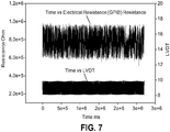
- FIG. 11 Surface resistivity during stretching was measured using the two point probe method shown in Figure 11 .
- the middle and the right photos in Figure 12 show the sample with silver paints and wire connects before and after inserting in the clamp, respectively.
- the left photo in Figure 12 shows the clamp for the bending test. For the case of bending experiments, birefringence and mechanical data was not collected.
- a picture of a large area electrically conducting film prepared using this technology is shown in Figure 13 .
- Figure 14 provides photographs of the optical microscopy (left) and SEM image (right) of the as-spun nanofibers.
- Optical microscopy image reveals the randomly distributed nature of the fine nanofibrous network whereas SEM shows that the average diameter of the fibers is around 300 nm lower than the wavelength of the visible spectrum 400 to 700 nm.
- the nanofiber mats show a white to lightly bluish color, due to the porous structure which causes light scattering.
- the wet film appears transparent.
- the small diameter of the fibers along with fairly good refractive index matching with the solution cast polymer film render the final hybrid films transparent.
- the UV-visible light transmittance measurements show that for both PMMA and PI substrate film the transmittance is higher than 85% at 550 nm transmittance. In fact, the transmittance changes depending on the used substrate and the transmittance decrease by the embedded nanofibers is almost negligible for a film with 2 k ⁇ /sq surface resistivity.
- Figure 15 shows a PMMA film that was stretched to 300% at a temperature of 105°C about 20°C above Tg of the film. During stretching, the surface resistivity of the film was monitored. In the stretching process, the surface resistivity of the film increases very slightly at 300%. As a comparison, the PET film coated with 250A ITO was stretched to the same elongation. In the case of ITO coated PET, a catastrophic failure happened before 20% which was due to the brittle nature of inorganic ITO material. SEM pictures detail the conductive network in the stretched films survived large strains whereas the ITO coated films were broken immediately.
- conductive nanofiber embedded PMMA film was bended around a rod with a diameter of 6 mm which causes the film to undergo a maximum curvature of 1/3 mm -1 .
- the conductivity of the film maintains at the same level after bending for more than 1000 times.
- the present invention utilizes a combination of any one or more spinnable polymer (i.e., polymer that can be electrospun), whether conductive or not, and at least one electrically conductive material (as described above and reiterated herein below) to produce fibers, nanofibers, structures, and/or nanostructures that are conductive.
- spinnable polymer i.e., polymer that can be electrospun
- electrically conductive material as described above and reiterated herein below
- the amount of the at least one electrically conductive material, when present in the electrospinning solution is in the range from about 0.1 weight percent to about 50 weight percent, or from about 0.5 weight percent to about 47.5 weight percent, or from about 1 weight percent to about 45 weight percent, or from about 2.5 weight percent to about 40 weight percent, or from about 5 weight percent to about 35 weight percent, or from about 7.5 weight percent to about 30 weight percent, or from about 10 weight percent to about 27.5 weight percent, or from about 12.5 weight percent to about 25 weight percent, or from about 15 weight percent to about 22.5 weight percent, or even from about 17.5 weight percent to about 20 weight percent.
- the at least one electrically conductive material, when present in the electrospinning solution is less than about 10 weight percent.
- individual numerical range values, or limits can be combined to form additional non-disclosed, or new, ranges.
- suitable electrically conductive materials for utilization in, or with, an electrospinning solution of a polymer include, but are not limited to, carbon-based components (e.g. , including, but not limited to, carbon nanotubes or nanostructures, precursor compounds that generate conductive carbon compounds or structures upon heating and/or graphitization), conductive metal particles and/or nanoparticles (e.g ., gold, silver, copper, etc. nanoparticles), conductive metal alloy particles and/or nanoparticles, or a combination of two or more thereof.
- carbon-based components e.g. , including, but not limited to, carbon nanotubes or nanostructures, precursor compounds that generate conductive carbon compounds or structures upon heating and/or graphitization
- conductive metal particles and/or nanoparticles e.g ., gold, silver, copper, etc. nanoparticles
- conductive metal alloy particles and/or nanoparticles e.g., gold, silver, copper, etc. nanoparticles
- a manufacturing method in accordance with the present invention permits the orientation of the conductive fibers and/or conductive nanofibers using an array of electrodes on which the nanofibers are spun, thereby permitting the nanofibers to be oriented on at least one surface including, but not limited to, exhibiting some orientation gradient across the thickness direction.
- the present invention relies on a continuous corrugated collector (see Figure 18 ) which provides a plurality of ground electrode pairs separated by non-conducting air medium. Such corrugated surfaces can be readily prepared and are available as a carrier belt ideal for continuous processing in roll-to-roll (R2R) operations.
- Figure 19 is a drawing of a multi-nozzle electrospinning platform similar to that of Figure 10 which can be utilized to deposit oriented nanofibers on the corrugated surface of Figure 18 .
- the structures of Figures 18 and 19 can be utilized, in one embodiment, to produce fibers, nanofibers, or structures formed therefrom that contain oriented fibers thereby yielding an increase in electrical conductivity in one direction based on the nature of the orientation of the fibers/nanofibers.
- the present invention utilizes non-oriented and/or randomly oriented fibers/nanofibers. In this case, the electrically conductivity of such fibers are generally, or substantially, equal in all directions.
- roll-to-roll (R2R) equipment equipped with a multi-nozzle spinning platform and corrugated conducting carrier can be used for continuous production of fiber and/or nanofiber mats that contain oriented fibers/nanofibers.
- R2R roll-to-roll
- An exemplary setup for producing such structures is illustrated in Figure 18 .
- Orientation of the fibers can also be induced mechanically either by a fast rotating or moving target in the form of a cylinder ( Sundaray, B., et al.; (2004); Electrospinning of Continuous Aligned Polymer Fibers; Applied Physics Letters; 84(7); pp. 1222 to 1224 ) or a belt. Combining the idea of fast rotating drum and corrugation would cause both the mechanical and electrical alignment of nanofibers leading to improved orientation of the electrically conductive electrospun fibers/nanofibers.
- a suitable cylinder is shown in Figure 20 .
- the fibers/nanofibers can be deposited in the aligned configuration for a long period of time.
- the efficiency of alignment decreases due to the fact that the fibers insulate the collector.
- a negative voltage can be applied to the target.
- Figure 21 illustrates another possibility for collecting oriented fibers/nanofibers via an electrospinning process.
- a corrugated collector is utilized in an electrospinning device so as to facilitate the orientation, or desired alignment, of the fibers/nanofibers so produced.
- the present invention relates to a flexible and electrically conductive polymer film comprising: at least one electrically conductive nanofiber, or nanofiber structure, embedded in, located on, or attached to at least one polymer film, wherein the at least one electrically conductive nanofiber, or nanofiber structure, is formed from a electrospinning process and wherein the at least one polymer film is flexible.
- the present invention relates to a method for producing a flexible and electrically conductive polymer film comprising the steps of: (A) preparing at least one electrospinnable polymer composition; (B) electrospinning the at least one electrospinnable polymer composition to produce at least one electrically conductive nanofiber, or nanofiber structure, to produce an electrically conductive electrospun structure; and (C) casting at least one polymer film onto the electrically conductive electrospun structure of Step (B) to yield a flexible and electrically conductive polymer film, wherein the electrospinnable polymer composition of Step (A) is itself electrically conductive, or the electrospinnable polymer solution contains at least one electrically conductive material therein, and wherein the at least one electrically conductive nanofiber, or nanofiber structure, is located on or in, or is partially embedded in, the cast film of Step (C).
- the present invention relates to a method for producing a flexible and electrically conductive polymer film comprising the steps of: (i) casting at least one polymer film onto a suitable surface; (ii) preparing at least one electrospinnable polymer composition; (iii) electrospinning the at least one electrospinnable polymer composition to produce at least one electrically conductive nanofiber, or nanofiber structure, on, in, or partially embedded in the cast film of Step (i), wherein the electrospinnable polymer composition of Step (ii) is either itself electrically conductive, or the electrospinnable polymer solution contains at least one electrically conductive material therein.
Landscapes
- Engineering & Computer Science (AREA)
- Mechanical Engineering (AREA)
- Textile Engineering (AREA)
- Manufacture Of Macromolecular Shaped Articles (AREA)
- Non-Insulated Conductors (AREA)
- Laminated Bodies (AREA)
- Compositions Of Macromolecular Compounds (AREA)
- Spinning Methods And Devices For Manufacturing Artificial Fibers (AREA)
- Reinforced Plastic Materials (AREA)
- Nonwoven Fabrics (AREA)
Claims (22)
- Flexibler, dehnbarer transparenter und elektrisch leitfähiger Polymerfilm, umfassend:eine Nanofaserstruktur, die vollständig oder teilweise in mindestens einen flexiblen transparenten Polymerfilm eingebettet ist, wobei der flexible, dehnbare, transparente Polymerfilm aus einem dielektrischen Polymer gebildet ist und die Nanofaserstruktur aus ununterbrochenen elektrogesponnenen Nanofasern, die aus elektrisch leitfähigen Material in einem Polymer bestehen, derart gebildet ist, dass die Nanofaserstruktur den Film elektrisch leitfähig macht und offene Räume definiert, um die Transparenz in dem flexiblen, dehnbaren, transparenten und elektrisch leitfähigen Polymerfilm zu erhalten.
- Polymerfilm nach Anspruch 1, wobei die Nanofaserstruktur aus einer oder mehreren Nanofasern mit einem durchschnittlichen Durchmesser im Bereich von ungefähr 1 Nanometer bis ungefähr 25000 Nanometer gebildet ist.
- Polymerfilm nach Anspruch 2, wobei die Nanofaserstruktur aus einer oder mehreren Nanofasern mit einem durchschnittlichen Durchmesser im Bereich von ungefähr 1 Nanometer bis ungefähr 500 Nanometer gebildet ist.
- Polymerfilm nach Anspruch 1, wobei der flexible, dehnbare, transparente und elektrisch leitfähige Polymerfilm eine Lichtdurchlässigkeit im sichtbaren Lichtbereich von mindestens ungefähr 50 Prozent aufweist.
- Polymerfilm nach Anspruch 4, wobei der flexible, dehnbare, transparente und elektrisch leitfähige Polymerfilm eine Lichtdurchlässigkeit im sichtbaren Lichtbereich von mindestens ungefähr 75 Prozent aufweist.
- Polymerfilm nach Anspruch 1, wobei die Nanofaserstruktur aus einer elektrisch leitfähigen Verbindung ausgewählt aus Polyanilinen (PANI), Polypyrollidinen, Polyfluoren(en), Polypyrenen, Polyazulenen, Polynaphthalinen, Polypyrrol(en) (PPY), Polycarbazolen, Polyindolen, Polyazepinen, Polythiophen(en) (PT), Polyphenylensulfid (PPS), Polyacetylen(en) (PAC), Polyphenylenvinyl(en) (PPV), Poly-3,4-Ethylendioxythiophen (PEDOT), Polystyrolsulfonat (PSS), einem Gemisch aus PEDOT/PSS oder geeigneten Mischungen von beliebigen zwei oder mehr davon gebildet ist.
- Polymerfilm nach Anspruch 1, wobei das mindestens eine elektrisch leitfähige Material aus einer oder mehreren kohlenstoffbasierten Komponenten, einem oder mehreren leitfähigen Metall-Nanopartikeln oder -Nanostrukturen, einem oder mehreren leitfähigen Metallpartikeln oder -strukturen, einem oder mehreren leitfähigen Metalllegierungs-Nanopartikeln oder -Nanostrukturen, einem oder mehreren leitfähigen Metalllegierungspartikeln oder -strukturen oder einer Kombination von zwei oder mehr davon ausgewählt ist.
- Polymerfilm nach Anspruch 1, wobei das Polymer der die Nanofaserstruktur bildenden Nanofasern aus einem oder mehreren Polyethylenoxiden, einem oder mehreren Polyimiden oder einer Kombination von zwei oder mehr davon ausgewählt ist.
- Polymerfilm nach Anspruch 1, wobei mindestens ein elektrisch leitfähiges Material in der Nanofaserstruktur im Bereich von ungefähr 0,1 Gewichtsprozent bis ungefähr 50 Gewichtsprozent vorhanden ist.
- Polymerfilm nach Anspruch 9, wobei mindestens ein elektrisch leitfähiges Material in der Nanofaserstruktur im Bereich von ungefähr 5 Gewichtsprozent bis ungefähr 35 Gewichtsprozent vorhanden ist.
- Polymerfilm nach Anspruch 1, wobei die Nanofaserstruktur orientierte Nanofasern enthält.
- Verfahren zum Herstellen eines flexiblen, dehnbaren, transparenten und elektrisch leitfähigen Polymerfilms, die Schritte umfassend:(i) Gießen mindestens eines flexiblen, transparenten und elektrisch leitfähigen Polymerfilms auf eine geeignete Oberfläche;(ii) Herstellen mindestens einer elektrospinnbaren Polymerzusammensetzung aus einer Kombination von mindestens einem elektrisch leitfähigen Material und mindestens einem elektrospinnbaren Polymer;(iii) direktes Elektrospinnen der mindestens einen elektrospinnbaren Polymerzusammensetzung auf den Polymerfilm von Schritt (i), wobei das Polymer von Schritt (i) eine flüssige Schicht derart bereitstellt, dass die mindestens eine elektrospinnbare Polymerzusammensetzung teilweise oder vollständig in die flüssige Schicht eindringt, um eine oder mehrere elektrisch leitfähige ununterbrochene Nanofasern herzustellen, die vollständig oder teilweise in den gegossenen Film von Schritt (i) eingebettet sind,wobei die eine oder die mehreren elektrisch leitfähigen ununterbrochenen Nanofasern den Film elektrisch leitfähig machen und offene Räume definieren, um die Transparenz in dem flexiblen, transparenten und elektrisch leitfähigen Polymerfilm zu erhalten.
- Verfahren nach Anspruch 12, wobei die eine oder die mehreren elektrisch leitfähigen Nanofasern einen durchschnittlichen Durchmesser im Bereich von ungefähr 1 Nanometer bis ungefähr 25000 Nanometer aufweisen.
- Verfahren nach Anspruch 13, wobei die eine oder die mehreren elektrisch leitfähigen Nanofasern einen durchschnittlichen Durchmesser im Bereich von ungefähr 10 Nanometer bis ungefähr 500 Nanometer aufweisen.
- Verfahren nach Anspruch 12, wobei der Polymerfilm eine Lichtdurchlässigkeit im sichtbaren Lichtbereich von mindestens 50 Prozent aufweist.
- Verfahren nach Anspruch 15, wobei der Polymerfilm eine Lichtdurchlässigkeit im sichtbaren Lichtbereich von mindestens 75 Prozent aufweist.
- Verfahren nach Anspruch 12, wobei das mindestens eine elektrisch leitfähige Material aus einer oder aus mehreren kohlenstoffbasierten Komponenten, einem oder mehreren leitfähigen Metall-Nanopartikeln oder - Nanostrukturen, einem oder mehreren leitfähigen Metallpartikeln oder -strukturen, einem oder mehreren leitfähigen Metalllegierungs-Nanopartikeln oder - Nanostrukturen, einem oder mehreren leitfähigen Metalllegierungspartikeln oder -strukturen oder einer Kombination von zwei oder mehr davon ausgewählt ist.
- Verfahren nach Anspruch 12, wobei das mindestens eine elektrospinnbare Polymer aus einem oder mehreren Polyethylenoxiden, einem oder mehreren Polyimiden oder einer Kombination von zwei oder mehr davon ausgewählt ist.
- Verfahren nach Anspruch 12, wobei mindestens ein elektrisch leitfähiges Material in der einen oder den mehreren elektrisch leitfähigen Nanofasern im Bereich von ungefähr 0,1 Gewichtsprozent bis ungefähr 50 Gewichtsprozent vorhanden ist.
- Verfahren nach Anspruch 19, wobei mindestens ein elektrisch leitfähiges Material in der einen oder den mehreren elektrisch leitfähigen Nanofasern im Bereich von ungefähr 5 Gewichtsprozent bis ungefähr 35 Gewichtsprozent vorhanden ist.
- Verfahren nach Anspruch 12, wobei mindestens eine elektrospinnbare Polymerzusammensetzung aus einer Mischung aus einem oder mehreren Polyethylenoxiden, Poly-3,4-Ethylendioxythiophen und Polystyrensulfonat gebildet ist.
- Verfahren nach Anspruch 12, wobei in dem Schritt des direkten Elektrospinnens die eine oder die mehreren elektrisch leitfähigen Nanofasern in Richtung auf einen gewellten Kollektor derart elektrogesponnen werden, dass die Nanofasern orientierte Nanofasern sind.
Applications Claiming Priority (3)
| Application Number | Priority Date | Filing Date | Title |
|---|---|---|---|
| US22576709P | 2009-07-15 | 2009-07-15 | |
| US22580209P | 2009-07-15 | 2009-07-15 | |
| PCT/US2010/042185 WO2011008993A1 (en) | 2009-07-15 | 2010-07-15 | Manufacturing of multifunctional electrically conductive/transparent/flexible films |
Publications (3)
| Publication Number | Publication Date |
|---|---|
| EP2454069A1 EP2454069A1 (de) | 2012-05-23 |
| EP2454069A4 EP2454069A4 (de) | 2015-08-12 |
| EP2454069B1 true EP2454069B1 (de) | 2017-08-23 |
Family
ID=43449808
Family Applications (1)
| Application Number | Title | Priority Date | Filing Date |
|---|---|---|---|
| EP10800569.5A Not-in-force EP2454069B1 (de) | 2009-07-15 | 2010-07-15 | Herstellung von multifunktionalen elektrisch leitfähigen bzw. transparenten bzw. flexiblen filmen |
Country Status (7)
| Country | Link |
|---|---|
| US (1) | US10350795B2 (de) |
| EP (1) | EP2454069B1 (de) |
| JP (2) | JP2012533657A (de) |
| CN (1) | CN102470570B (de) |
| CA (1) | CA2768218C (de) |
| IN (1) | IN2012DN00408A (de) |
| WO (1) | WO2011008993A1 (de) |
Families Citing this family (26)
| Publication number | Priority date | Publication date | Assignee | Title |
|---|---|---|---|---|
| BR112012001564A2 (pt) | 2009-07-20 | 2015-09-01 | Janssen Biotech Inc | Diferenciação de células tronco embrionárias humanas. |
| JP2012156255A (ja) * | 2011-01-25 | 2012-08-16 | Tokyo Institute Of Technology | 光電変換素子およびその作製方法 |
| US8586148B2 (en) * | 2011-03-23 | 2013-11-19 | The Regents Of The University Of California | Low voltage near-field electrospinning method and device |
| JP2013196910A (ja) * | 2012-03-20 | 2013-09-30 | Denso Corp | 非水電解液二次電池 |
| CN103928632A (zh) * | 2013-01-16 | 2014-07-16 | 海洋王照明科技股份有限公司 | 一种阳极及其制备方法和有机电致发光器件及其制备方法 |
| TWI631580B (zh) | 2013-02-20 | 2018-08-01 | 國立大學法人東京工業大學 | 具有]導電性奈米線網絡之導電性基板,及其製造方法 |
| WO2015002825A1 (en) | 2013-07-02 | 2015-01-08 | The University Of Connecticut | Electrically conductive synthetic fiber and fibrous substrate, method of making, and use thereof |
| US10333176B2 (en) | 2013-08-12 | 2019-06-25 | The University Of Akron | Polymer electrolyte membranes for rechargeable batteries |
| US10099938B2 (en) | 2013-12-12 | 2018-10-16 | Samsung Electronics Co., Ltd. | Electrically conductive thin films |
| JP6362345B2 (ja) * | 2014-02-10 | 2018-07-25 | キヤノン株式会社 | 構造体、電子機器部材、構造体の製造方法 |
| US10002686B2 (en) | 2014-03-12 | 2018-06-19 | The University Of Connecticut | Method of infusing fibrous substrate with conductive organic particles and conductive polymer; and conductive fibrous substrates prepared therefrom |
| JP6333018B2 (ja) * | 2014-03-28 | 2018-05-30 | キヤノン株式会社 | ナノファイバ構造体とこれを用いた捕集装置、ナノファイバ構造体の製造方法 |
| KR102251775B1 (ko) | 2014-07-18 | 2021-05-12 | 삼성전자주식회사 | 전극 구조체 및 이를 사용하는 접촉 감지 센서 |
| US10438715B2 (en) | 2014-11-12 | 2019-10-08 | Samsung Electronics Co., Ltd. | Nanostructure, method of preparing the same, and panel units comprising the nanostructure |
| KR102375891B1 (ko) | 2014-12-24 | 2022-03-16 | 삼성전자주식회사 | 투명전극 및 이를 포함하는 전자 소자 |
| EP3286767B1 (de) | 2015-04-23 | 2021-03-24 | The University of Connecticut | Hochleitfähige polymerfilmzusammensetzungen aus nanopartikelinduzierter phasentrennung von gegenionvorlagen aus leitfähigen polymeren |
| EP3286372B1 (de) | 2015-04-23 | 2022-06-01 | The University of Connecticut | Dehnbare organische metalle, zusammensetzung und verwendung |
| CN104894750B (zh) * | 2015-06-16 | 2017-05-03 | 青岛大学 | 一种力敏可拉伸电纺图案化导电纳米纤维膜及其制备方法 |
| CN107039101B (zh) | 2015-09-25 | 2020-03-10 | 三星电子株式会社 | 电导体、一维-二维混杂结构体、和包括其的电子器件 |
| KR20170037572A (ko) | 2015-09-25 | 2017-04-04 | 삼성전자주식회사 | 도전체, 그 제조 방법, 및 이를 포함하는 전자 소자 |
| US10883814B2 (en) | 2016-05-09 | 2021-01-05 | South Dakota Board Of Regents | Highly stretchable strain sensor for human motion monitoring |
| CN105887333B (zh) * | 2016-06-12 | 2017-11-17 | 东华大学 | 三维曲折纳米纤维膜及其静电纺丝方法 |
| TWI637036B (zh) * | 2017-02-06 | 2018-10-01 | 國立台灣大學 | 有機發光半導體及彈性體之摻合體以及其所製成之奈米纖維及薄膜 |
| US11043728B2 (en) | 2018-04-24 | 2021-06-22 | University Of Connecticut | Flexible fabric antenna system comprising conductive polymers and method of making same |
| KR102612862B1 (ko) * | 2021-12-17 | 2023-12-15 | 인하대학교 산학협력단 | 고신축 전도성 마이크로 와이어 어레이 제조 장치 및 이를 이용한 고신축 전도성 마이크로 와이어 어레이 제조 방법 |
| CN114858877B (zh) * | 2022-04-18 | 2023-06-16 | 武汉大学 | 一种超柔软自支撑纳米网电极及其制备方法与应用 |
Citations (1)
| Publication number | Priority date | Publication date | Assignee | Title |
|---|---|---|---|---|
| WO2007022226A2 (en) * | 2005-08-12 | 2007-02-22 | Cambrios Technologies Corporation | Nanowires-based transparent conductors |
Family Cites Families (14)
| Publication number | Priority date | Publication date | Assignee | Title |
|---|---|---|---|---|
| US3360394A (en) * | 1964-01-24 | 1967-12-26 | Burlington Industries Inc | Process for forming breathable polyurethane coating on a textile fabric and the resulting product |
| KR950003362A (ko) * | 1993-07-21 | 1995-02-16 | 마에다 가츠노스케 | 섬유강화 열가소성수지구조물과 그 제조방법 및 압출기 |
| US6800155B2 (en) * | 2000-02-24 | 2004-10-05 | The United States Of America As Represented By The Secretary Of The Army | Conductive (electrical, ionic and photoelectric) membrane articlers, and method for producing same |
| JP2006123360A (ja) * | 2004-10-29 | 2006-05-18 | Oji Paper Co Ltd | 積層体およびその製造方法 |
| US8889054B2 (en) * | 2005-10-17 | 2014-11-18 | The University Of Akron | Hybrid manufacturing platform to produce multifunctional polymeric films |
| US8455088B2 (en) * | 2005-12-23 | 2013-06-04 | Boston Scientific Scimed, Inc. | Spun nanofiber, medical devices, and methods |
| US20070286982A1 (en) * | 2006-06-12 | 2007-12-13 | Higgins Kenneth B | Surface coverings and methods |
| JP2008075010A (ja) * | 2006-09-22 | 2008-04-03 | Mitsubishi Chemicals Corp | 樹脂複合体 |
| EP2095442A4 (de) * | 2006-11-29 | 2011-08-17 | Mahiar Hamedi | In stoffe integrierte elektronische schaltkreise |
| US7923922B2 (en) * | 2006-12-27 | 2011-04-12 | Ut-Battelle, Llc | Transparent conductive nano-composites |
| DE102007040762A1 (de) * | 2007-08-29 | 2009-03-05 | Bayer Materialscience Ag | Vorrichtung und Verfahren zur Herstellung von elektrisch leitenden Nanostrukturen mittels Elektrospinnen |
| WO2009084418A1 (ja) * | 2007-12-27 | 2009-07-09 | Idemitsu Kosan Co., Ltd. | ポリアニリン複合体、その組成物及び成形体 |
| JPWO2009084419A1 (ja) * | 2007-12-27 | 2011-05-19 | 出光興産株式会社 | ポリアニリン複合体、その組成物及び成形体 |
| CA2722552A1 (en) * | 2008-04-25 | 2009-10-29 | The University Of Akron | Nanofiber enhanced functional film manufacturing method using melt film casting |
-
2010
- 2010-07-15 JP JP2012520796A patent/JP2012533657A/ja active Pending
- 2010-07-15 WO PCT/US2010/042185 patent/WO2011008993A1/en active Application Filing
- 2010-07-15 IN IN408DEN2012 patent/IN2012DN00408A/en unknown
- 2010-07-15 EP EP10800569.5A patent/EP2454069B1/de not_active Not-in-force
- 2010-07-15 CN CN201080031758.1A patent/CN102470570B/zh not_active Expired - Fee Related
- 2010-07-15 US US13/383,988 patent/US10350795B2/en active Active
- 2010-07-15 CA CA2768218A patent/CA2768218C/en active Active
-
2015
- 2015-08-21 JP JP2015163570A patent/JP2015214714A/ja active Pending
Patent Citations (1)
| Publication number | Priority date | Publication date | Assignee | Title |
|---|---|---|---|---|
| WO2007022226A2 (en) * | 2005-08-12 | 2007-02-22 | Cambrios Technologies Corporation | Nanowires-based transparent conductors |
Also Published As
| Publication number | Publication date |
|---|---|
| CN102470570A (zh) | 2012-05-23 |
| EP2454069A4 (de) | 2015-08-12 |
| WO2011008993A1 (en) | 2011-01-20 |
| EP2454069A1 (de) | 2012-05-23 |
| IN2012DN00408A (de) | 2015-08-21 |
| JP2012533657A (ja) | 2012-12-27 |
| CN102470570B (zh) | 2017-03-29 |
| CA2768218A1 (en) | 2011-01-20 |
| US10350795B2 (en) | 2019-07-16 |
| US20120153236A1 (en) | 2012-06-21 |
| CA2768218C (en) | 2018-02-20 |
| JP2015214714A (ja) | 2015-12-03 |
Similar Documents
| Publication | Publication Date | Title |
|---|---|---|
| EP2454069B1 (de) | Herstellung von multifunktionalen elektrisch leitfähigen bzw. transparenten bzw. flexiblen filmen | |
| US6800155B2 (en) | Conductive (electrical, ionic and photoelectric) membrane articlers, and method for producing same | |
| CN106782769B (zh) | 低粗糙度低方阻的柔性透明导电复合薄膜及其制备方法 | |
| Liu et al. | Electrospun PEDOT: PSS–PVA nanofiber based ultrahigh-strain sensors with controllable electrical conductivity | |
| Vohra et al. | Electroluminescence from conjugated polymer electrospun nanofibers in solution processable organic light-emitting diodes | |
| Mahdavi Varposhti et al. | Enhancement of β‐phase crystalline structure and piezoelectric properties of flexible PVDF/ionic liquid surfactant composite nanofibers for potential application in sensing and self‐powering | |
| Zhao et al. | Flexible, stretchable, transparent and electrically conductive polymer films via a hybrid electrospinning and solution casting process: In-plane anisotropic conductivity for electro-optical applications | |
| US8940194B2 (en) | Electrodes with electrospun fibers | |
| KR100947892B1 (ko) | 나노그레인/나노입자의 네트워크 구조를 가진도체금속산화물 막을 이용한 전도성전극, 이의 제조방법 및이를 이용한 수퍼캐패시터 | |
| Onggar et al. | Techniques and processes for the realization of electrically conducting textile materials from intrinsically conducting polymers and their application potential | |
| US9905332B2 (en) | Transparent conductive electrode and associated production method | |
| US20150280156A1 (en) | Transparent electrode and associated production method | |
| Wang et al. | Influence of ethylene glycol vapor annealing on structure and property of wet-spun PVA/PEDOT: PSS blend fiber | |
| US20220077378A1 (en) | Piezoelectric composite fiber | |
| Rhee et al. | Stretchable hole extraction layer for improved stability in perovskite solar cells | |
| Kang et al. | Ga and Ti co-doped In2O3 films for flexible amorphous transparent conducting oxides | |
| CN100335685C (zh) | 聚对苯乙炔纳米丝及其制备方法 | |
| CN108485234A (zh) | 一种基于有序导电网络结构的自愈合传感高分子复合材料及其制备方法 | |
| Chotimah et al. | The electrical properties of PEDOT: PSS nanofibers | |
| Rathore et al. | Effect of pH Value on the Electrical Properties of PEDOT: PSS-Based Fiber Mats | |
| KR101384643B1 (ko) | 스프레이 코팅을 통해 제조된 β-상 PVDF 필름을 포함하는 발전소자 | |
| Ismail et al. | Effect of annealing temperature on electrical properties of poly (methyl methacrylate): titanium dioxide nanocomposite films using spin coating deposition technique | |
| Benbalit et al. | Metal-free and carbon-free flexible self-supporting thin film electrodes | |
| Lee et al. | Fabrication and characterization of aligned continuous polymeric electrospun nanofibers | |
| Anggoro et al. | Fabrication and characterization of PVA/TiO2 nanofibers on ITO glass using the electrospinning method |
Legal Events
| Date | Code | Title | Description |
|---|---|---|---|
| PUAI | Public reference made under article 153(3) epc to a published international application that has entered the european phase |
Free format text: ORIGINAL CODE: 0009012 |
|
| 17P | Request for examination filed |
Effective date: 20120113 |
|
| AK | Designated contracting states |
Kind code of ref document: A1 Designated state(s): AL AT BE BG CH CY CZ DE DK EE ES FI FR GB GR HR HU IE IS IT LI LT LU LV MC MK MT NL NO PL PT RO SE SI SK SM TR |
|
| DAX | Request for extension of the european patent (deleted) | ||
| RA4 | Supplementary search report drawn up and despatched (corrected) |
Effective date: 20150715 |
|
| RIC1 | Information provided on ipc code assigned before grant |
Ipc: B32B 33/00 20060101AFI20150709BHEP Ipc: B29C 39/20 20060101ALI20150709BHEP Ipc: B29D 7/01 20060101ALI20150709BHEP Ipc: D01D 5/08 20060101ALI20150709BHEP |
|
| 17Q | First examination report despatched |
Effective date: 20160517 |
|
| REG | Reference to a national code |
Ref country code: DE Ref legal event code: R079 Ref document number: 602010044690 Country of ref document: DE Free format text: PREVIOUS MAIN CLASS: B29C0039200000 Ipc: B32B0005020000 |
|
| RIC1 | Information provided on ipc code assigned before grant |
Ipc: B32B 5/02 20060101AFI20170313BHEP |
|
| GRAP | Despatch of communication of intention to grant a patent |
Free format text: ORIGINAL CODE: EPIDOSNIGR1 |
|
| INTG | Intention to grant announced |
Effective date: 20170421 |
|
| GRAS | Grant fee paid |
Free format text: ORIGINAL CODE: EPIDOSNIGR3 |
|
| GRAA | (expected) grant |
Free format text: ORIGINAL CODE: 0009210 |
|
| AK | Designated contracting states |
Kind code of ref document: B1 Designated state(s): AL AT BE BG CH CY CZ DE DK EE ES FI FR GB GR HR HU IE IS IT LI LT LU LV MC MK MT NL NO PL PT RO SE SI SK SM TR |
|
| REG | Reference to a national code |
Ref country code: GB Ref legal event code: FG4D |
|
| REG | Reference to a national code |
Ref country code: CH Ref legal event code: EP |
|
| REG | Reference to a national code |
Ref country code: AT Ref legal event code: REF Ref document number: 920880 Country of ref document: AT Kind code of ref document: T Effective date: 20170915 |
|
| REG | Reference to a national code |
Ref country code: IE Ref legal event code: FG4D |
|
| REG | Reference to a national code |
Ref country code: DE Ref legal event code: R096 Ref document number: 602010044690 Country of ref document: DE |
|
| REG | Reference to a national code |
Ref country code: NL Ref legal event code: MP Effective date: 20170823 |
|
| REG | Reference to a national code |
Ref country code: LT Ref legal event code: MG4D |
|
| REG | Reference to a national code |
Ref country code: AT Ref legal event code: MK05 Ref document number: 920880 Country of ref document: AT Kind code of ref document: T Effective date: 20170823 |
|
| PG25 | Lapsed in a contracting state [announced via postgrant information from national office to epo] |
Ref country code: AT Free format text: LAPSE BECAUSE OF FAILURE TO SUBMIT A TRANSLATION OF THE DESCRIPTION OR TO PAY THE FEE WITHIN THE PRESCRIBED TIME-LIMIT Effective date: 20170823 Ref country code: LT Free format text: LAPSE BECAUSE OF FAILURE TO SUBMIT A TRANSLATION OF THE DESCRIPTION OR TO PAY THE FEE WITHIN THE PRESCRIBED TIME-LIMIT Effective date: 20170823 Ref country code: NO Free format text: LAPSE BECAUSE OF FAILURE TO SUBMIT A TRANSLATION OF THE DESCRIPTION OR TO PAY THE FEE WITHIN THE PRESCRIBED TIME-LIMIT Effective date: 20171123 Ref country code: SE Free format text: LAPSE BECAUSE OF FAILURE TO SUBMIT A TRANSLATION OF THE DESCRIPTION OR TO PAY THE FEE WITHIN THE PRESCRIBED TIME-LIMIT Effective date: 20170823 Ref country code: NL Free format text: LAPSE BECAUSE OF FAILURE TO SUBMIT A TRANSLATION OF THE DESCRIPTION OR TO PAY THE FEE WITHIN THE PRESCRIBED TIME-LIMIT Effective date: 20170823 Ref country code: HR Free format text: LAPSE BECAUSE OF FAILURE TO SUBMIT A TRANSLATION OF THE DESCRIPTION OR TO PAY THE FEE WITHIN THE PRESCRIBED TIME-LIMIT Effective date: 20170823 Ref country code: FI Free format text: LAPSE BECAUSE OF FAILURE TO SUBMIT A TRANSLATION OF THE DESCRIPTION OR TO PAY THE FEE WITHIN THE PRESCRIBED TIME-LIMIT Effective date: 20170823 |
|
| PG25 | Lapsed in a contracting state [announced via postgrant information from national office to epo] |
Ref country code: ES Free format text: LAPSE BECAUSE OF FAILURE TO SUBMIT A TRANSLATION OF THE DESCRIPTION OR TO PAY THE FEE WITHIN THE PRESCRIBED TIME-LIMIT Effective date: 20170823 Ref country code: IS Free format text: LAPSE BECAUSE OF FAILURE TO SUBMIT A TRANSLATION OF THE DESCRIPTION OR TO PAY THE FEE WITHIN THE PRESCRIBED TIME-LIMIT Effective date: 20171223 Ref country code: LV Free format text: LAPSE BECAUSE OF FAILURE TO SUBMIT A TRANSLATION OF THE DESCRIPTION OR TO PAY THE FEE WITHIN THE PRESCRIBED TIME-LIMIT Effective date: 20170823 Ref country code: BG Free format text: LAPSE BECAUSE OF FAILURE TO SUBMIT A TRANSLATION OF THE DESCRIPTION OR TO PAY THE FEE WITHIN THE PRESCRIBED TIME-LIMIT Effective date: 20171123 Ref country code: GR Free format text: LAPSE BECAUSE OF FAILURE TO SUBMIT A TRANSLATION OF THE DESCRIPTION OR TO PAY THE FEE WITHIN THE PRESCRIBED TIME-LIMIT Effective date: 20171124 Ref country code: PL Free format text: LAPSE BECAUSE OF FAILURE TO SUBMIT A TRANSLATION OF THE DESCRIPTION OR TO PAY THE FEE WITHIN THE PRESCRIBED TIME-LIMIT Effective date: 20170823 |
|
| PG25 | Lapsed in a contracting state [announced via postgrant information from national office to epo] |
Ref country code: RO Free format text: LAPSE BECAUSE OF FAILURE TO SUBMIT A TRANSLATION OF THE DESCRIPTION OR TO PAY THE FEE WITHIN THE PRESCRIBED TIME-LIMIT Effective date: 20170823 Ref country code: DK Free format text: LAPSE BECAUSE OF FAILURE TO SUBMIT A TRANSLATION OF THE DESCRIPTION OR TO PAY THE FEE WITHIN THE PRESCRIBED TIME-LIMIT Effective date: 20170823 Ref country code: CZ Free format text: LAPSE BECAUSE OF FAILURE TO SUBMIT A TRANSLATION OF THE DESCRIPTION OR TO PAY THE FEE WITHIN THE PRESCRIBED TIME-LIMIT Effective date: 20170823 |
|
| REG | Reference to a national code |
Ref country code: DE Ref legal event code: R097 Ref document number: 602010044690 Country of ref document: DE |
|
| PG25 | Lapsed in a contracting state [announced via postgrant information from national office to epo] |
Ref country code: EE Free format text: LAPSE BECAUSE OF FAILURE TO SUBMIT A TRANSLATION OF THE DESCRIPTION OR TO PAY THE FEE WITHIN THE PRESCRIBED TIME-LIMIT Effective date: 20170823 Ref country code: SK Free format text: LAPSE BECAUSE OF FAILURE TO SUBMIT A TRANSLATION OF THE DESCRIPTION OR TO PAY THE FEE WITHIN THE PRESCRIBED TIME-LIMIT Effective date: 20170823 Ref country code: IT Free format text: LAPSE BECAUSE OF FAILURE TO SUBMIT A TRANSLATION OF THE DESCRIPTION OR TO PAY THE FEE WITHIN THE PRESCRIBED TIME-LIMIT Effective date: 20170823 Ref country code: SM Free format text: LAPSE BECAUSE OF FAILURE TO SUBMIT A TRANSLATION OF THE DESCRIPTION OR TO PAY THE FEE WITHIN THE PRESCRIBED TIME-LIMIT Effective date: 20170823 |
|
| PLBE | No opposition filed within time limit |
Free format text: ORIGINAL CODE: 0009261 |
|
| STAA | Information on the status of an ep patent application or granted ep patent |
Free format text: STATUS: NO OPPOSITION FILED WITHIN TIME LIMIT |
|
| 26N | No opposition filed |
Effective date: 20180524 |
|
| PG25 | Lapsed in a contracting state [announced via postgrant information from national office to epo] |
Ref country code: SI Free format text: LAPSE BECAUSE OF FAILURE TO SUBMIT A TRANSLATION OF THE DESCRIPTION OR TO PAY THE FEE WITHIN THE PRESCRIBED TIME-LIMIT Effective date: 20170823 |
|
| REG | Reference to a national code |
Ref country code: CH Ref legal event code: PL |
|
| PG25 | Lapsed in a contracting state [announced via postgrant information from national office to epo] |
Ref country code: MC Free format text: LAPSE BECAUSE OF FAILURE TO SUBMIT A TRANSLATION OF THE DESCRIPTION OR TO PAY THE FEE WITHIN THE PRESCRIBED TIME-LIMIT Effective date: 20170823 Ref country code: LU Free format text: LAPSE BECAUSE OF NON-PAYMENT OF DUE FEES Effective date: 20180715 |
|
| REG | Reference to a national code |
Ref country code: BE Ref legal event code: MM Effective date: 20180731 |
|
| REG | Reference to a national code |
Ref country code: IE Ref legal event code: MM4A |
|
| PG25 | Lapsed in a contracting state [announced via postgrant information from national office to epo] |
Ref country code: IE Free format text: LAPSE BECAUSE OF NON-PAYMENT OF DUE FEES Effective date: 20180715 Ref country code: CH Free format text: LAPSE BECAUSE OF NON-PAYMENT OF DUE FEES Effective date: 20180731 Ref country code: FR Free format text: LAPSE BECAUSE OF NON-PAYMENT OF DUE FEES Effective date: 20180731 Ref country code: LI Free format text: LAPSE BECAUSE OF NON-PAYMENT OF DUE FEES Effective date: 20180731 |
|
| PG25 | Lapsed in a contracting state [announced via postgrant information from national office to epo] |
Ref country code: BE Free format text: LAPSE BECAUSE OF NON-PAYMENT OF DUE FEES Effective date: 20180731 |
|
| PGFP | Annual fee paid to national office [announced via postgrant information from national office to epo] |
Ref country code: DE Payment date: 20190910 Year of fee payment: 10 |
|
| PGFP | Annual fee paid to national office [announced via postgrant information from national office to epo] |
Ref country code: GB Payment date: 20190719 Year of fee payment: 10 |
|
| PG25 | Lapsed in a contracting state [announced via postgrant information from national office to epo] |
Ref country code: MT Free format text: LAPSE BECAUSE OF NON-PAYMENT OF DUE FEES Effective date: 20180715 |
|
| PG25 | Lapsed in a contracting state [announced via postgrant information from national office to epo] |
Ref country code: TR Free format text: LAPSE BECAUSE OF FAILURE TO SUBMIT A TRANSLATION OF THE DESCRIPTION OR TO PAY THE FEE WITHIN THE PRESCRIBED TIME-LIMIT Effective date: 20170823 |
|
| PG25 | Lapsed in a contracting state [announced via postgrant information from national office to epo] |
Ref country code: HU Free format text: LAPSE BECAUSE OF FAILURE TO SUBMIT A TRANSLATION OF THE DESCRIPTION OR TO PAY THE FEE WITHIN THE PRESCRIBED TIME-LIMIT; INVALID AB INITIO Effective date: 20100715 Ref country code: PT Free format text: LAPSE BECAUSE OF FAILURE TO SUBMIT A TRANSLATION OF THE DESCRIPTION OR TO PAY THE FEE WITHIN THE PRESCRIBED TIME-LIMIT Effective date: 20170823 |
|
| PG25 | Lapsed in a contracting state [announced via postgrant information from national office to epo] |
Ref country code: MK Free format text: LAPSE BECAUSE OF NON-PAYMENT OF DUE FEES Effective date: 20170823 Ref country code: CY Free format text: LAPSE BECAUSE OF FAILURE TO SUBMIT A TRANSLATION OF THE DESCRIPTION OR TO PAY THE FEE WITHIN THE PRESCRIBED TIME-LIMIT Effective date: 20170823 |
|
| PG25 | Lapsed in a contracting state [announced via postgrant information from national office to epo] |
Ref country code: AL Free format text: LAPSE BECAUSE OF FAILURE TO SUBMIT A TRANSLATION OF THE DESCRIPTION OR TO PAY THE FEE WITHIN THE PRESCRIBED TIME-LIMIT Effective date: 20170823 |
|
| REG | Reference to a national code |
Ref country code: DE Ref legal event code: R119 Ref document number: 602010044690 Country of ref document: DE |
|
| GBPC | Gb: european patent ceased through non-payment of renewal fee |
Effective date: 20200715 |
|
| PG25 | Lapsed in a contracting state [announced via postgrant information from national office to epo] |
Ref country code: GB Free format text: LAPSE BECAUSE OF NON-PAYMENT OF DUE FEES Effective date: 20200715 |
|
| PG25 | Lapsed in a contracting state [announced via postgrant information from national office to epo] |
Ref country code: DE Free format text: LAPSE BECAUSE OF NON-PAYMENT OF DUE FEES Effective date: 20210202 |