EP2453569A1 - Inverter device relay-connecting member - Google Patents
Inverter device relay-connecting member Download PDFInfo
- Publication number
- EP2453569A1 EP2453569A1 EP10796982A EP10796982A EP2453569A1 EP 2453569 A1 EP2453569 A1 EP 2453569A1 EP 10796982 A EP10796982 A EP 10796982A EP 10796982 A EP10796982 A EP 10796982A EP 2453569 A1 EP2453569 A1 EP 2453569A1
- Authority
- EP
- European Patent Office
- Prior art keywords
- relay
- connecting member
- inverter device
- male tab
- contact
- Prior art date
- Legal status (The legal status is an assumption and is not a legal conclusion. Google has not performed a legal analysis and makes no representation as to the accuracy of the status listed.)
- Granted
Links
Images



Classifications
-
- H—ELECTRICITY
- H01—ELECTRIC ELEMENTS
- H01R—ELECTRICALLY-CONDUCTIVE CONNECTIONS; STRUCTURAL ASSOCIATIONS OF A PLURALITY OF MUTUALLY-INSULATED ELECTRICAL CONNECTING ELEMENTS; COUPLING DEVICES; CURRENT COLLECTORS
- H01R31/00—Coupling parts supported only by co-operation with counterpart
- H01R31/06—Intermediate parts for linking two coupling parts, e.g. adapter
-
- H—ELECTRICITY
- H01—ELECTRIC ELEMENTS
- H01R—ELECTRICALLY-CONDUCTIVE CONNECTIONS; STRUCTURAL ASSOCIATIONS OF A PLURALITY OF MUTUALLY-INSULATED ELECTRICAL CONNECTING ELEMENTS; COUPLING DEVICES; CURRENT COLLECTORS
- H01R13/00—Details of coupling devices of the kinds covered by groups H01R12/70 or H01R24/00 - H01R33/00
- H01R13/66—Structural association with built-in electrical component
- H01R13/6608—Structural association with built-in electrical component with built-in single component
- H01R13/6633—Structural association with built-in electrical component with built-in single component with inductive component, e.g. transformer
-
- H—ELECTRICITY
- H02—GENERATION; CONVERSION OR DISTRIBUTION OF ELECTRIC POWER
- H02K—DYNAMO-ELECTRIC MACHINES
- H02K11/00—Structural association of dynamo-electric machines with electric components or with devices for shielding, monitoring or protection
- H02K11/30—Structural association with control circuits or drive circuits
- H02K11/33—Drive circuits, e.g. power electronics
-
- H—ELECTRICITY
- H01—ELECTRIC ELEMENTS
- H01R—ELECTRICALLY-CONDUCTIVE CONNECTIONS; STRUCTURAL ASSOCIATIONS OF A PLURALITY OF MUTUALLY-INSULATED ELECTRICAL CONNECTING ELEMENTS; COUPLING DEVICES; CURRENT COLLECTORS
- H01R13/00—Details of coupling devices of the kinds covered by groups H01R12/70 or H01R24/00 - H01R33/00
- H01R13/62—Means for facilitating engagement or disengagement of coupling parts or for holding them in engagement
- H01R13/629—Additional means for facilitating engagement or disengagement of coupling parts, e.g. aligning or guiding means, levers, gas pressure electrical locking indicators, manufacturing tolerances
- H01R13/631—Additional means for facilitating engagement or disengagement of coupling parts, e.g. aligning or guiding means, levers, gas pressure electrical locking indicators, manufacturing tolerances for engagement only
- H01R13/6315—Additional means for facilitating engagement or disengagement of coupling parts, e.g. aligning or guiding means, levers, gas pressure electrical locking indicators, manufacturing tolerances for engagement only allowing relative movement between coupling parts, e.g. floating connection
-
- H—ELECTRICITY
- H02—GENERATION; CONVERSION OR DISTRIBUTION OF ELECTRIC POWER
- H02K—DYNAMO-ELECTRIC MACHINES
- H02K5/00—Casings; Enclosures; Supports
- H02K5/04—Casings or enclosures characterised by the shape, form or construction thereof
- H02K5/22—Auxiliary parts of casings not covered by groups H02K5/06-H02K5/20, e.g. shaped to form connection boxes or terminal boxes
- H02K5/225—Terminal boxes or connection arrangements
-
- H—ELECTRICITY
- H02—GENERATION; CONVERSION OR DISTRIBUTION OF ELECTRIC POWER
- H02M—APPARATUS FOR CONVERSION BETWEEN AC AND AC, BETWEEN AC AND DC, OR BETWEEN DC AND DC, AND FOR USE WITH MAINS OR SIMILAR POWER SUPPLY SYSTEMS; CONVERSION OF DC OR AC INPUT POWER INTO SURGE OUTPUT POWER; CONTROL OR REGULATION THEREOF
- H02M7/00—Conversion of AC power input into DC power output; Conversion of DC power input into AC power output
- H02M7/003—Constructional details, e.g. physical layout, assembly, wiring or busbar connections
Definitions
- the present invention relates to an improvement in an inverter device relay-connecting member which is accommodated in an inverter device including a circuit provided with a switching element, and which electrically connects the circuit and an output terminal of the inverter device.
- IPM intelligent power module
- a semiconductor chip serving as a switching element such as an IGBT (Insulated Gate Bipolar Transistor)
- IGBT Insulated Gate Bipolar Transistor
- control board for controlling driving of the semiconductor chip.
- the intelligent power module is provided with an output electrode which outputs power of the circuit board.
- the inverter device is provided with an output terminal which outputs its power to an electric motor.
- the output electrode and the output terminal are electrically connected through a bus bar serving as a relay-connecting member. Specifically, one end of the bus bar is fastened to the output electrode (for example, a bus bar) by means of a bolt, and another end of the bus bar is fastened to the output terminal (for example, a bus bar) by means of a bolt so that the output electrode and the output terminal are electrically connected.
- the relay-connecting member is provided with a current detector which detects a current that flows therethrough.
- the current detector includes a core through which the bus bar is passed, a magnetic flux density detection element such as a Hall element which is arranged in a gap portion of the core, and a circuit board on which the magnetic flux density detection element is mounted.
- the current detector when a current flows through the bus bar, the current causes generation of a magnetic field within the core, and the magnetic flux density detection element converts the intensity of that magnetic field into a voltage signal to thereby allow detection of a current value.
- JP 2006-194650 A describes a current sensor which is accommodated in a power converter, and which detects a current of a bus bar that connects a semiconductor module and an output terminal block.
- the current sensor has a case which is formed of a resin such that the bus bar and a core through which the bus bar is passed form an integral structure, and a Hall element and a circuit board are attached to this case.
- a bus bar serving as a relay-connecting member is connected to an output electrode of an inverter circuit and to an output terminal of an inverter device, respectively, by bolt fastening. Therefore, there is a problem in that, when a plurality of (for example, three, for three-phase alternating current power) relay-connecting members are to be attached, the fastening process is time-consuming.
- a bus bar serving as a relay-connecting member must have a region for bolt fastening and a region in which a core is attached so as not to overlap with the region for bolt fastening. Therefore, as the size of the bus bar is large in the length direction, there is a problem in that a large space is required for accommodating the bus bar in the inverter device.
- An object of the present invention is to provide an inverter device relay-connecting member in which an electrical connection between an output electrode of an inverter circuit and an output terminal of an inverter device can be achieved with a simple structure.
- an object of the present invention is to provide an inverter device relay-connecting member which can adapt to reduction in size of an inverter device.
- an inverter device relay-connecting member which is accommodated in an inverter device including a circuit provided with a switching element, and which electrically connects the circuit and an output terminal of the inverter device, the inverter device relay-connecting member comprising a relay terminal which is fit-connected to an output electrode of the circuit and a male tab of the output terminal; and a housing for accommodating the relay terminal, the housing being formed of a resin to form an integral structure having therein a current detector for detecting a current of the relay terminal.
- the relay terminal may have contact portions which are able to come into contact with the male tab even if the male tab that is inserted is displaced from a normal position in an axial direction, and which are able to come into contact with the male tab even if the male tab that is inserted is displaced from the normal position in a first orthogonal direction that is orthogonal to the axial direction.
- the contact portions may be supported by a pair of elastic support pieces which have an interval from each other in the first orthogonal direction, and which are displaceable in the first orthogonal direction, and the contact portions may come into contact with side surfaces of the male tab that is inserted.
- the contact portions are further able to come into contact with the male tab even if the male tab that is inserted is displaced from the normal position in a second orthogonal direction that is orthogonal to the axial direction and the first orthogonal direction.
- the length of the contact portions in the second orthogonal direction is greater than the length of the male tab in the same direction.
- the current detector may include a core through which the relay terminal is passed; a magnetic flux density detection element arranged in a gap portion of the core; and a circuit board on which the magnetic flux density detection element is mounted.
- an electrical connection between an output electrode of an inverter circuit and an output terminal of an inverter device can be achieved with a simple structure. Further, by employing the inverter device relay-connecting member according to the present invention, an inverter device can be reduced in size.
- An inverter device 10 includes an intelligent power module 12 (indicated by a broken line in FIG. 1 ), an output terminal 14, and a relay-connecting member 16 which electrically connects the intelligent power module 12 and the output terminal 14.
- the intelligent power module 12 and the relay-connecting member 16 are housed in a case 18 (indicated by alternate long and short dashed lines in FIG. 1 ) of the inverter device 10, and the output terminal 14 is provided on the case 18 of the inverter device 10.
- the intelligent power module 12 includes semiconductor chips 20 serving as switching elements, an inverter circuit board 22 on the front side of which the semiconductor chips 20 are mounted, a heatsink 24 provided on the back side of the inverter circuit board 22 for dissipating heat generated from the semiconductor chips 20, and a control board (not shown) for controlling driving of the semiconductor chips 20.
- the semiconductor chips 20 are switching elements used for an inverter or a booster converter, and include an IGBT, a power transistor, a thyristor, and the like.
- An electrical circuit is formed on the front side of the inverter circuit board 22, and the semiconductor chips 20 are electrically connected on this electrical circuit by means of soldering.
- the heatsink 24 is formed of aluminum or copper, which are superior in thermal conductivity and have light weight.
- the heatsink 24 has a channel (not shown) through which a coolant flows.
- an electronic device (not shown) may be provided in contact with the bottom plate of the heatsink 24. Examples of the electronic device include a DC/DC converter and a reactor, and heat generated from this electronic device can also be dissipated by the heatsink 24.
- the intelligent power module 12 has an output electrode 28 which outputs power from the semiconductor chips 20 through a wire 26.
- the output electrode 28 according to the present embodiment is a flat-shaped bus bar. This bus bar is electrically connected to the relay-connecting member 16.
- the output electrode 28 is not limited to a flat-shaped bus bar, but may also be a pin-shaped conductor component.
- the output terminal 14 is connected to an electric motor (not shown), and power output from the intelligent power module 12 is output to the electric motor.
- the electric motor is a motor which is driven to rotate with supply thereto of three-phase alternating current power obtained by conversion from direct current power performed in the inverter device 10.
- the output terminal 14 according to the present embodiment has a pin-shaped male tab 30.
- the male tab 30 is electrically connected to the relay-connecting member 16.
- the shape of the male tab 30 is not limited to a pin shape, and may also be a flat shape.
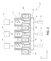
- a structure of the relay-connecting member 16 according to the present embodiment will be described with reference to FIGs. 2 to 6 .
- a relay-connecting member 16 having three electric lines for three-phase alternating current power will be described.
- the number of electric lines is given as one example, and the present invention is not limited to the number, three, of electric lines, but may also be applied to a relay terminal component having six electric lines, which integrates two sets of electric lines for three-phase alternating current power.
- the relay-connecting member 16 has three relay terminals 32, each of which is fit-connected to the output electrode 28 and the male tab 30 of the output terminal 14. With this structure, by simply inserting the output electrode 28 and the male tab 30 of the output terminal 14 into the relay-connecting member 16, it is possible to easily electrically connect the output electrode 28 and the male tab 30 of the output terminal 14 through the relay terminal 32. Because bolt fastening is not performed, it is unnecessary to arrange the relay terminals 32 with an interval determined in consideration of space for tools used for bolt fastening being provided therebetween. Therefore, it is possible to arrange the relay terminals 32 with a smaller interval being provided therebetween, and it is possible to reduce the size of the relay-connecting member 16.
- relay-connecting member 16 it is possible to attach a core so as to overlap with a region in which a relay terminal 32 is fit-connected to an output electrode 28 and a male tab 30. As such, it is possible to shorten the length of the relay-connecting member 16 in the axial direction, and it is possible to reduce the size of the relay-connecting member 16.
- the relay-connecting member 16 has a housing 34 for accommodating the relay terminals 32 in a manner such that the relay terminals 32 arranged with a predetermined interval being provided therebetween are isolated from each other.
- the housing 34 is formed of a resin to form an integral structure having therein a current detector 36 for detecting a current that flows through the relay terminals 32.
- the current detector 36 includes cores 38a and 38b which are provided such that relay terminals 32 located on the respective ends pass through the cores 38a and 38b, magnetic flux density detection elements (not shown) which are arranged in gap portions (not shown) of the cores 38a and 38b, and a circuit board 39 on which these magnetic flux density detection elements are mounted.
- the current detector 36 when a current flows through the relay terminals 32, the current causes a magnetic field to be generated within the cores 38a and 38b, and the magnetic flux density detection elements convert the intensity of that magnetic field into a voltage signal so that the current detector 36 detects a current value.
- the current value is output from the current detector 36 to the control board of the intelligent power module 12, and the control board controls driving of the semiconductor chip 20 based on the current value.
- the current detector 36 is formed of a resin integrally with the housing 34, when the relay-connecting member 16 is to be attached, the process of passing the relay terminals 32 through the respective cores 38a and 38b is eliminated.
- a conventional current detector is supported by means of, for example, an attachment component for the intelligent power module, because the current detector 36 according to the present embodiment is attached integrally with the housing 34 of the relay-connecting member 16, it is possible to save space for the conventional attachment component.
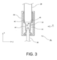
- FIG. 3 shows a state in which the relay-connecting member 16 is fit-connected to the output electrode 28 and the output terminal 14.
- This diagram and FIGs. 4 to 6 focus on one relay terminal 32 of the relay-connecting member 16, and show a state in which this relay terminal 32 is connected to the output electrode 28 and the male tab 30 of the output terminal 14.
- the relay terminal 32 has first contact portions 40 which come into contact with the output electrode 28 inserted into the relay-connecting member 16, and second contact portions 42 which come into contact with the male tab 30 inserted into the relay-connecting member 16.
- the first contact portions 40 and the second contact portions 42 are supported by elastic support pieces 44.
- the first contact portions 40 are supported by the elastic support pieces 44 so as to come into contact with an end surface of the output electrode 28.
- the first contact portions 40 come into contact with the end surface of the output electrode 28 so as to restrict the movement of the output electrode 28 toward the inner side of the relay terminal 32 in the axial direction; in other words, in the x direction.
- the second contact portions 42 are supported by the elastic support pieces 44 so as to come into contact with side surfaces of the male tab 30.
- the second contact portions 42 do not restrict the movement of the male tab 30 toward the inner side of the relay terminal 32 in the axial direction; in other words, in the x direction.
- the elastic support pieces 44 and the first and second contact portions 40 and 42 according to the present embodiment are integrally formed.
- the elastic support pieces 44 are formed to extend in the x direction, and are provided to oppose each other with an interval being provided therebetween in the y direction that is orthogonal to the x direction (shown in FIG. 3 ). In other words, the first contact portions 40 and the second contact portions 42 are respectively provided to oppose each other with an interval being provided therebetween in the y direction.
- the elastic support pieces 44 are plate-shaped elastic components which can tilt within the housing 34 in the y direction, and are attached to the housing 34 only at an end portion on the side from which the output electrode 28 is inserted. As a result, portions of the elastic support pieces 44 on the side from which the male tab 30 is inserted are displaceable in the y direction. In other words, the second contact portions 42 are displaceable in the y direction.
- FIG. 6 is a diagram corresponding to FIG. 3 as viewed from the direction of arrow A shown in Fig. 3 .
- a length L1 of the second contact portions 42 in the z direction that is orthogonal to the x direction and the y direction is greater than a length L2 of the male tab 30 in the z direction.
- the relay terminal 32 can permit that positional displacement to maintain an electrical connection between the output electrode 28 and the male tab 30.
- the present invention is not limited to this structure, and the first contact portions 40 may be configured in such a manner.
- the present invention is not limited to this structure, and the output terminal 14 may be provided on a case of an electric motor.
Landscapes
- Engineering & Computer Science (AREA)
- Power Engineering (AREA)
- Microelectronics & Electronic Packaging (AREA)
- Inverter Devices (AREA)
- Measuring Instrument Details And Bridges, And Automatic Balancing Devices (AREA)
Abstract
Description
- The present invention relates to an improvement in an inverter device relay-connecting member which is accommodated in an inverter device including a circuit provided with a switching element, and which electrically connects the circuit and an output terminal of the inverter device.
- Inverter devices for controlling power to be supplied to an electric motor have heretofore been known. Such an inverter device includes an intelligent power module (IPM) including a semiconductor chip serving as a switching element such as an IGBT (Insulated Gate Bipolar Transistor), an inverter circuit board on which the semiconductor chip is mounted, and a control board for controlling driving of the semiconductor chip.
- The intelligent power module is provided with an output electrode which outputs power of the circuit board. The inverter device is provided with an output terminal which outputs its power to an electric motor. There are examples in which the output electrode and the output terminal are electrically connected through a bus bar serving as a relay-connecting member. Specifically, one end of the bus bar is fastened to the output electrode (for example, a bus bar) by means of a bolt, and another end of the bus bar is fastened to the output terminal (for example, a bus bar) by means of a bolt so that the output electrode and the output terminal are electrically connected.
- Further, there are examples in which the relay-connecting member is provided with a current detector which detects a current that flows therethrough. The current detector includes a core through which the bus bar is passed, a magnetic flux density detection element such as a Hall element which is arranged in a gap portion of the core, and a circuit board on which the magnetic flux density detection element is mounted. In this current detector, when a current flows through the bus bar, the current causes generation of a magnetic field within the core, and the magnetic flux density detection element converts the intensity of that magnetic field into a voltage signal to thereby allow detection of a current value.
-
JP 2006-194650 A -
- Patent Document 1:
JP 2006-194650 A - For a conventional inverter device, a bus bar serving as a relay-connecting member is connected to an output electrode of an inverter circuit and to an output terminal of an inverter device, respectively, by bolt fastening. Therefore, there is a problem in that, when a plurality of (for example, three, for three-phase alternating current power) relay-connecting members are to be attached, the fastening process is time-consuming.
- Further, for a conventional inverter device, it is necessary to provide an interval determined in consideration of space for tools used for bolt fastening between adjacently arranged relay-connecting members. Therefore, there is a problem in that a large space is required for accommodating relay-connecting members in the inverter device.
- Further, for a conventional inverter device, in order that a bus bar serving as a relay-connecting member can reliably pass through a core of a current detector when the relay-connecting member is attached, it is necessary to form a pass-through portion of the core to have a size with a sufficient margin with respect to the bus bar. Therefore, as the size of the core is large, there is a problem in that a large space is required for accommodating the core in the inverter device.
- Further, for a conventional inverter device, a bus bar serving as a relay-connecting member must have a region for bolt fastening and a region in which a core is attached so as not to overlap with the region for bolt fastening. Therefore, as the size of the bus bar is large in the length direction, there is a problem in that a large space is required for accommodating the bus bar in the inverter device.
- An object of the present invention is to provide an inverter device relay-connecting member in which an electrical connection between an output electrode of an inverter circuit and an output terminal of an inverter device can be achieved with a simple structure.
- Further, an object of the present invention is to provide an inverter device relay-connecting member which can adapt to reduction in size of an inverter device.
- According to one aspect of the present invention, there is provided an inverter device relay-connecting member which is accommodated in an inverter device including a circuit provided with a switching element, and which electrically connects the circuit and an output terminal of the inverter device, the inverter device relay-connecting member comprising a relay terminal which is fit-connected to an output electrode of the circuit and a male tab of the output terminal; and a housing for accommodating the relay terminal, the housing being formed of a resin to form an integral structure having therein a current detector for detecting a current of the relay terminal.
- Further, the relay terminal may have contact portions which are able to come into contact with the male tab even if the male tab that is inserted is displaced from a normal position in an axial direction, and which are able to come into contact with the male tab even if the male tab that is inserted is displaced from the normal position in a first orthogonal direction that is orthogonal to the axial direction.
- Further, the contact portions may be supported by a pair of elastic support pieces which have an interval from each other in the first orthogonal direction, and which are displaceable in the first orthogonal direction, and the contact portions may come into contact with side surfaces of the male tab that is inserted.
- Further, it is preferable that the contact portions are further able to come into contact with the male tab even if the male tab that is inserted is displaced from the normal position in a second orthogonal direction that is orthogonal to the axial direction and the first orthogonal direction.
- Further, it is preferable that the length of the contact portions in the second orthogonal direction is greater than the length of the male tab in the same direction.
- Further, the current detector may include a core through which the relay terminal is passed; a magnetic flux density detection element arranged in a gap portion of the core; and a circuit board on which the magnetic flux density detection element is mounted.
- By employing the inverter device relay-connecting member according to the present invention, an electrical connection between an output electrode of an inverter circuit and an output terminal of an inverter device can be achieved with a simple structure. Further, by employing the inverter device relay-connecting member according to the present invention, an inverter device can be reduced in size.
-
- [
FIG. 1] FIG. 1 shows a structure of an inverter device according to an embodiment of the present invention. - [
FIG. 2] FIG. 2 shows a structure of a relay-connecting member according to the embodiment of the present invention. - [
FIG. 3] FIG. 3 shows a state in which the relay-connecting member is fit-connected to an output electrode and an output terminal. - [
FIG. 4] FIG. 4 shows a state for a case where a male tab of the output terminal is displaced from a normal position in the x direction. - [
FIG. 5] FIG. 5 shows a state for a case where the male tab of the output terminal is displaced from the normal position in the y direction. - [
FIG. 6] FIG. 6 shows a state for a case where the male tab of the output terminal is displaced from the normal position in the z direction. -
- 10
- INVERTER DEVICE
- 12
- INTELLIGENT POWER MODULE
- 14
- OUTPUT TERMINAL
- 16
- RELAY-CONNECTING MEMBER
- 18
- CASE
- 20
- SEMICONDUCTOR CHIP
- 22
- INVERTER CIRCUIT BOARD
- 24
- HEATSINK
- 26
- WIRE
- 28
- OUTPUT ELECTRODE
- 30
- MALE TAB
- 32
- RELAY TERMINAL
- 34
- HOUSING
- 36
- CURRENT DETECTOR
- 38
- CORE
- 39
- CIRCUIT BOARD
- 40
- FIRST CONTACT PORTION
- 42
- SECOND CONTACT PORTION
- 44
- ELASTIC SUPPORT PIECE
- An embodiment of an inverter device relay-connecting member according to the present invention will be described below with reference to the drawings. First, a structure of an inverter device will be described with reference to
FIG. 1 . - An
inverter device 10 includes an intelligent power module 12 (indicated by a broken line inFIG. 1 ), anoutput terminal 14, and a relay-connectingmember 16 which electrically connects theintelligent power module 12 and theoutput terminal 14. Theintelligent power module 12 and the relay-connectingmember 16 are housed in a case 18 (indicated by alternate long and short dashed lines inFIG. 1 ) of theinverter device 10, and theoutput terminal 14 is provided on thecase 18 of theinverter device 10. - The
intelligent power module 12 includessemiconductor chips 20 serving as switching elements, aninverter circuit board 22 on the front side of which the semiconductor chips 20 are mounted, aheatsink 24 provided on the back side of theinverter circuit board 22 for dissipating heat generated from the semiconductor chips 20, and a control board (not shown) for controlling driving of the semiconductor chips 20. - The semiconductor chips 20 are switching elements used for an inverter or a booster converter, and include an IGBT, a power transistor, a thyristor, and the like.
- An electrical circuit is formed on the front side of the
inverter circuit board 22, and the semiconductor chips 20 are electrically connected on this electrical circuit by means of soldering. - The
heatsink 24 is formed of aluminum or copper, which are superior in thermal conductivity and have light weight. Theheatsink 24 has a channel (not shown) through which a coolant flows. Further, an electronic device (not shown) may be provided in contact with the bottom plate of theheatsink 24. Examples of the electronic device include a DC/DC converter and a reactor, and heat generated from this electronic device can also be dissipated by theheatsink 24. - Further, the
intelligent power module 12 has anoutput electrode 28 which outputs power from the semiconductor chips 20 through awire 26. Theoutput electrode 28 according to the present embodiment is a flat-shaped bus bar. This bus bar is electrically connected to the relay-connectingmember 16. However, theoutput electrode 28 is not limited to a flat-shaped bus bar, but may also be a pin-shaped conductor component. - The
output terminal 14 is connected to an electric motor (not shown), and power output from theintelligent power module 12 is output to the electric motor. The electric motor is a motor which is driven to rotate with supply thereto of three-phase alternating current power obtained by conversion from direct current power performed in theinverter device 10. Theoutput terminal 14 according to the present embodiment has a pin-shapedmale tab 30. Themale tab 30 is electrically connected to the relay-connectingmember 16. However, the shape of themale tab 30 is not limited to a pin shape, and may also be a flat shape. - Next, a structure of the relay-connecting
member 16 according to the present embodiment will be described with reference toFIGs. 2 to 6 . As an example, a relay-connectingmember 16 having three electric lines for three-phase alternating current power will be described. However, the number of electric lines is given as one example, and the present invention is not limited to the number, three, of electric lines, but may also be applied to a relay terminal component having six electric lines, which integrates two sets of electric lines for three-phase alternating current power. - The relay-connecting
member 16 has threerelay terminals 32, each of which is fit-connected to theoutput electrode 28 and themale tab 30 of theoutput terminal 14. With this structure, by simply inserting theoutput electrode 28 and themale tab 30 of theoutput terminal 14 into the relay-connectingmember 16, it is possible to easily electrically connect theoutput electrode 28 and themale tab 30 of theoutput terminal 14 through therelay terminal 32. Because bolt fastening is not performed, it is unnecessary to arrange therelay terminals 32 with an interval determined in consideration of space for tools used for bolt fastening being provided therebetween. Therefore, it is possible to arrange therelay terminals 32 with a smaller interval being provided therebetween, and it is possible to reduce the size of the relay-connectingmember 16. Further, because bolt fastening is not performed, it is unnecessary to separate a region for bolt fastening and a region in which a core is attached in a relay-connecting member, as described above in connection with conventional techniques. In other words, by employing the relay-connectingmember 16 according to the present embodiment, it is possible to attach a core so as to overlap with a region in which arelay terminal 32 is fit-connected to anoutput electrode 28 and amale tab 30. As such, it is possible to shorten the length of the relay-connectingmember 16 in the axial direction, and it is possible to reduce the size of the relay-connectingmember 16. - Further, the relay-connecting
member 16 has ahousing 34 for accommodating therelay terminals 32 in a manner such that therelay terminals 32 arranged with a predetermined interval being provided therebetween are isolated from each other. Thehousing 34 is formed of a resin to form an integral structure having therein acurrent detector 36 for detecting a current that flows through therelay terminals 32. - The
current detector 36 includescores relay terminals 32 located on the respective ends pass through thecores cores circuit board 39 on which these magnetic flux density detection elements are mounted. In thecurrent detector 36, when a current flows through therelay terminals 32, the current causes a magnetic field to be generated within thecores current detector 36 detects a current value. The current value is output from thecurrent detector 36 to the control board of theintelligent power module 12, and the control board controls driving of thesemiconductor chip 20 based on the current value. - As the
current detector 36 is formed of a resin integrally with thehousing 34, when the relay-connectingmember 16 is to be attached, the process of passing therelay terminals 32 through therespective cores cores cores member 16 can be reduced in size. Further, although a conventional current detector is supported by means of, for example, an attachment component for the intelligent power module, because thecurrent detector 36 according to the present embodiment is attached integrally with thehousing 34 of the relay-connectingmember 16, it is possible to save space for the conventional attachment component. -
FIG. 3 shows a state in which the relay-connectingmember 16 is fit-connected to theoutput electrode 28 and theoutput terminal 14. This diagram andFIGs. 4 to 6 , which will be described later, focus on onerelay terminal 32 of the relay-connectingmember 16, and show a state in which thisrelay terminal 32 is connected to theoutput electrode 28 and themale tab 30 of theoutput terminal 14. - The
relay terminal 32 hasfirst contact portions 40 which come into contact with theoutput electrode 28 inserted into the relay-connectingmember 16, andsecond contact portions 42 which come into contact with themale tab 30 inserted into the relay-connectingmember 16. Thefirst contact portions 40 and thesecond contact portions 42 are supported byelastic support pieces 44. Thefirst contact portions 40 are supported by theelastic support pieces 44 so as to come into contact with an end surface of theoutput electrode 28. Thefirst contact portions 40 come into contact with the end surface of theoutput electrode 28 so as to restrict the movement of theoutput electrode 28 toward the inner side of therelay terminal 32 in the axial direction; in other words, in the x direction. On the other hand, thesecond contact portions 42 are supported by theelastic support pieces 44 so as to come into contact with side surfaces of themale tab 30. As thesecond contact portions 42 come into contact with the side surfaces of themale tab 30, thesecond contact portions 42 do not restrict the movement of themale tab 30 toward the inner side of therelay terminal 32 in the axial direction; in other words, in the x direction. Theelastic support pieces 44 and the first andsecond contact portions - The
elastic support pieces 44 are formed to extend in the x direction, and are provided to oppose each other with an interval being provided therebetween in the y direction that is orthogonal to the x direction (shown inFIG. 3 ). In other words, thefirst contact portions 40 and thesecond contact portions 42 are respectively provided to oppose each other with an interval being provided therebetween in the y direction. Theelastic support pieces 44 are plate-shaped elastic components which can tilt within thehousing 34 in the y direction, and are attached to thehousing 34 only at an end portion on the side from which theoutput electrode 28 is inserted. As a result, portions of theelastic support pieces 44 on the side from which themale tab 30 is inserted are displaceable in the y direction. In other words, thesecond contact portions 42 are displaceable in the y direction. - With this structure, as shown in
FIG. 4 , even if the insertedmale tab 30 is displaced from the normal position in the x direction, thesecond contact portions 42 can come into contact with themale tab 30. Further, as shown inFIG. 5 , even if the insertedmale tab 30 is displaced from the normal position in the y direction, thesecond contact portions 42 can come into contact with themale tab 30. -
FIG. 6 is a diagram corresponding toFIG. 3 as viewed from the direction of arrow A shown inFig. 3 . As shown inFIG. 6 , a length L1 of thesecond contact portions 42 in the z direction that is orthogonal to the x direction and the y direction is greater than a length L2 of themale tab 30 in the z direction. As such, even if the insertedmale tab 30 is displaced from the normal position in the z direction, thesecond contact portions 42 can come into contact with themale tab 30. - By employing the relay-connecting
member 16 according to the present embodiment, even if a positional displacement occurs between theoutput electrode 28 and theoutput terminal 14 during assembly, therelay terminal 32 can permit that positional displacement to maintain an electrical connection between theoutput electrode 28 and themale tab 30. - Although, with reference to the above-described embodiment, there has been described a structure in which the
second contact portions 42 are configured to be able to come into contact with themale tab 30 which is displaced in various directions, the present invention is not limited to this structure, and thefirst contact portions 40 may be configured in such a manner. - Although, with reference to the above-described embodiment, there has been described a structure in which the
output terminal 14 is provided on thecase 18 of theinverter device 10, the present invention is not limited to this structure, and theoutput terminal 14 may be provided on a case of an electric motor.
Claims (6)
- An inverter device relay-connecting member which is accommodated in an inverter device including a circuit provided with a switching element, and which electrically connects the circuit and an output terminal of the inverter device, the inverter device relay-connecting member comprising:a relay terminal which is fit-connected to an output electrode of the circuit and a male tab of the output terminal; anda housing for accommodating the relay terminal, the housing being formed of a resin to form an integral structure having therein a current detector for detecting a current of the relay terminal.
- The inverter device relay-connecting member according to claim 1, wherein
the relay terminal has contact portions which are able to come into contact with the male tab even if the male tab that is inserted is displaced from a normal position in an axial direction, and which are able to come into contact with the male tab even if the male tab that is inserted is displaced from the normal position in a first orthogonal direction that is orthogonal to the axial direction. - The inverter device relay-connecting member according to claim 2, wherein
the contact portions are supported by a pair of elastic support pieces which have an interval from each other in the first orthogonal direction, and which are displaceable in the first orthogonal direction, and
the contact portions come into contact with side surfaces of the male tab that is inserted. - The inverter device relay-connecting member according to claim 3, wherein
the contact portions are further able to come into contact with the male tab even if the male tab that is inserted is displaced from the normal position in a second orthogonal direction that is orthogonal to the axial direction and the first orthogonal direction. - The inverter device relay-connecting member according to claim 4, wherein
a length of the contact portions in the second orthogonal direction is greater than a length of the male tab in the same direction. - The inverter device relay-connecting member according to claim 1, wherein
the current detector includes:a core through which the relay terminal is passed;a magnetic flux density detection element arranged in a gap portion of the core; anda circuit board on which the magnetic flux density detection element is mounted.
Applications Claiming Priority (2)
| Application Number | Priority Date | Filing Date | Title |
|---|---|---|---|
| JP2009159518A JP4708487B2 (en) | 2009-07-06 | 2009-07-06 | Inverter relay connection member |
| PCT/JP2010/059693 WO2011004671A1 (en) | 2009-07-06 | 2010-06-08 | Inverter device relay-connecting member |
Publications (3)
| Publication Number | Publication Date |
|---|---|
| EP2453569A1 true EP2453569A1 (en) | 2012-05-16 |
| EP2453569A4 EP2453569A4 (en) | 2012-05-16 |
| EP2453569B1 EP2453569B1 (en) | 2013-07-24 |
Family
ID=43429097
Family Applications (1)
| Application Number | Title | Priority Date | Filing Date |
|---|---|---|---|
| EP10796982.6A Not-in-force EP2453569B1 (en) | 2009-07-06 | 2010-06-08 | Inverter device relay-connecting member |
Country Status (5)
| Country | Link |
|---|---|
| US (1) | US8811050B2 (en) |
| EP (1) | EP2453569B1 (en) |
| JP (1) | JP4708487B2 (en) |
| CN (1) | CN102474170A (en) |
| WO (1) | WO2011004671A1 (en) |
Cited By (1)
| Publication number | Priority date | Publication date | Assignee | Title |
|---|---|---|---|---|
| CN107069314A (en) * | 2017-04-19 | 2017-08-18 | 王萍 | One kind exempts from wiring and connects formula socket soon |
Families Citing this family (16)
| Publication number | Priority date | Publication date | Assignee | Title |
|---|---|---|---|---|
| JP6019474B2 (en) * | 2011-02-04 | 2016-11-02 | 矢崎総業株式会社 | Conductive path assembly |
| US8585422B2 (en) | 2011-04-15 | 2013-11-19 | Rockwell Automation Technologies, Inc. | System for connecting motor drives |
| JP5806134B2 (en) | 2012-01-23 | 2015-11-10 | トヨタ自動車株式会社 | Power converter |
| USD697032S1 (en) | 2012-02-09 | 2014-01-07 | Sumitomo Electric Industries, Ltd. | Relay bus bar with built-in current sensor |
| JP5982860B2 (en) | 2012-02-22 | 2016-08-31 | 住友電気工業株式会社 | Relay busbar device with built-in current sensor for automobiles |
| JP5672259B2 (en) * | 2012-03-21 | 2015-02-18 | トヨタ自動車株式会社 | Power converter |
| US9160124B2 (en) | 2012-09-07 | 2015-10-13 | Apple Inc. | Compliant mount for connector |
| JP2014090629A (en) * | 2012-10-31 | 2014-05-15 | Denso Corp | Power conversion device |
| JP6117577B2 (en) * | 2013-03-15 | 2017-04-19 | 日立オートモティブシステムズ株式会社 | Electronic control unit |
| US9093804B2 (en) * | 2013-10-04 | 2015-07-28 | Rockwell Automation Technologies, Inc. | Apparatus for connecting a shared DC bus link |
| US9882421B2 (en) * | 2015-05-14 | 2018-01-30 | Rockwell Automation Technologies, Inc. | Method and apparatus for increasing current capacity of a distributed drive system |
| TWI658680B (en) * | 2017-11-30 | 2019-05-01 | 財團法人工業技術研究院 | Integrated power connecting device of driving controller coupling with electric power |
| JP7047445B2 (en) * | 2018-02-16 | 2022-04-05 | 株式会社デンソー | Power converter |
| JP7091945B2 (en) * | 2018-08-28 | 2022-06-28 | 住友電装株式会社 | Power relay device |
| JP7342766B2 (en) * | 2020-03-31 | 2023-09-12 | 株式会社豊田自動織機 | electric compressor |
| WO2025195735A1 (en) * | 2024-03-19 | 2025-09-25 | Robert Bosch Gmbh | Contacting arrangement for two spatially separated electrical components |
Family Cites Families (29)
| Publication number | Priority date | Publication date | Assignee | Title |
|---|---|---|---|---|
| US4597025A (en) | 1980-07-10 | 1986-06-24 | Eaton Corporation | Minimum size, integral, A.C. overload current sensing, remote power controller |
| JP3407485B2 (en) * | 1995-07-25 | 2003-05-19 | アイシン・エィ・ダブリュ株式会社 | Inverter device and transistor module with current sensor |
| JP3010422B2 (en) | 1995-09-20 | 2000-02-21 | 矢崎総業株式会社 | Busbar structure of electrical junction box |
| JP3351502B2 (en) * | 1996-09-20 | 2002-11-25 | 矢崎総業株式会社 | Connector with built-in current sensor |
| JPH10225140A (en) * | 1997-02-10 | 1998-08-21 | Denso Corp | Inverter |
| JPH11121067A (en) * | 1997-10-16 | 1999-04-30 | Toyota Motor Corp | Terminal block with built-in current sensor |
| US6414867B2 (en) * | 2000-02-16 | 2002-07-02 | Hitachi, Ltd. | Power inverter |
| JP3642012B2 (en) * | 2000-07-21 | 2005-04-27 | 株式会社日立製作所 | Semiconductor device, power conversion device and automobile |
| JP2003167009A (en) * | 2001-12-03 | 2003-06-13 | Stanley Electric Co Ltd | Current detector |
| US7187568B2 (en) * | 2002-01-16 | 2007-03-06 | Rockwell Automation Technologies, Inc. | Power converter having improved terminal structure |
| JP3651444B2 (en) * | 2002-02-27 | 2005-05-25 | 株式会社日立製作所 | Power converter |
| DE10317580B4 (en) * | 2002-04-18 | 2010-09-16 | Hitachi, Ltd. | Electric inverter device with a liquid channel and electric vehicle with such an inverter device |
| KR100614011B1 (en) * | 2002-09-13 | 2006-08-21 | 아이신에이더블류 가부시키가이샤 | Drive device |
| US7005734B2 (en) * | 2003-05-05 | 2006-02-28 | Ixys Corporation | Double-sided cooling isolated packaged power semiconductor device |
| EP1589547A4 (en) * | 2003-09-18 | 2009-11-25 | Panasonic Corp | CAPACITOR BLOCK |
| US7289329B2 (en) * | 2004-06-04 | 2007-10-30 | Siemens Vdo Automotive Corporation | Integration of planar transformer and/or planar inductor with power switches in power converter |
| JP4034770B2 (en) | 2004-09-09 | 2008-01-16 | 株式会社ケーヒン | Power drive unit |
| JP2006092776A (en) * | 2004-09-21 | 2006-04-06 | Yazaki Corp | Device connection connector |
| JP2006194650A (en) * | 2005-01-12 | 2006-07-27 | Hitachi Ltd | Current sensor |
| JP2006310208A (en) * | 2005-05-02 | 2006-11-09 | Jst Mfg Co Ltd | Short-circuit connector |
| JP4487962B2 (en) * | 2006-03-23 | 2010-06-23 | 株式会社デンソー | Inverter device |
| US7717747B2 (en) * | 2006-11-06 | 2010-05-18 | Gm Global Technology Operations, Inc. | Power inverter connector having integrated current sensors |
| JP4899817B2 (en) * | 2006-11-17 | 2012-03-21 | トヨタ自動車株式会社 | Electrical equipment connection structure |
| JP5059527B2 (en) * | 2007-09-12 | 2012-10-24 | 株式会社オートネットワーク技術研究所 | Relay connector |
| JP2009140705A (en) * | 2007-12-05 | 2009-06-25 | Toyota Motor Corp | Relay terminal and vehicle drive device |
| JP4730751B2 (en) * | 2008-09-02 | 2011-07-20 | 日本特殊陶業株式会社 | Gas sensor and gas sensor unit |
| US7692525B1 (en) * | 2008-09-30 | 2010-04-06 | Rockwell Automation Technologies, Inc. | Power electronic module with an improved choke and methods of making same |
| CN102112060B (en) * | 2008-10-14 | 2013-02-06 | 奥林巴斯医疗株式会社 | Ultrasonic probe |
| US9004950B2 (en) * | 2010-06-08 | 2015-04-14 | Panasonic Intellectual Property Management Co., Ltd. | Card device and socket |
-
2009
- 2009-07-06 JP JP2009159518A patent/JP4708487B2/en not_active Expired - Fee Related
-
2010
- 2010-06-08 CN CN2010800306106A patent/CN102474170A/en active Pending
- 2010-06-08 US US13/320,890 patent/US8811050B2/en not_active Expired - Fee Related
- 2010-06-08 EP EP10796982.6A patent/EP2453569B1/en not_active Not-in-force
- 2010-06-08 WO PCT/JP2010/059693 patent/WO2011004671A1/en not_active Ceased
Cited By (1)
| Publication number | Priority date | Publication date | Assignee | Title |
|---|---|---|---|---|
| CN107069314A (en) * | 2017-04-19 | 2017-08-18 | 王萍 | One kind exempts from wiring and connects formula socket soon |
Also Published As
| Publication number | Publication date |
|---|---|
| CN102474170A (en) | 2012-05-23 |
| US20120063188A1 (en) | 2012-03-15 |
| WO2011004671A1 (en) | 2011-01-13 |
| EP2453569A4 (en) | 2012-05-16 |
| US8811050B2 (en) | 2014-08-19 |
| JP2011015586A (en) | 2011-01-20 |
| EP2453569B1 (en) | 2013-07-24 |
| JP4708487B2 (en) | 2011-06-22 |
Similar Documents
| Publication | Publication Date | Title |
|---|---|---|
| US8811050B2 (en) | Inverter device relay-connecting member | |
| JP5622043B2 (en) | Inverter device | |
| EP2015361B1 (en) | Semi conductor device | |
| CN110754033B (en) | Power conversion device | |
| US11894774B2 (en) | Power converter | |
| CN107223210B (en) | Device for integrated measurement of the current in a high-voltage contact of a hybrid module and hybrid module having the same | |
| JP2006230064A (en) | Power conversion unit | |
| EP3633722A1 (en) | Semiconductor power module | |
| CN115912972A (en) | Inverters with optimized electromagnetic characteristics | |
| CN109463033B (en) | Power conversion device | |
| US10755999B2 (en) | Multi-package top-side-cooling | |
| US20240188263A1 (en) | Power module for a converter with improved field shielding of signal pins | |
| JP4640213B2 (en) | Power semiconductor device and inverter bridge module using the same | |
| CN113826315B (en) | Power conversion device | |
| JP2011114872A (en) | Power conversion apparatus | |
| US11901837B2 (en) | Power control unit | |
| JP2009032997A (en) | Power module | |
| US12009758B2 (en) | Half-bridge for an electric drive of an electric vehicle or a hybrid vehicle, power module for an inverter and inverter | |
| WO2019189450A1 (en) | Power conversion device | |
| JP2002291261A (en) | Power converter | |
| JP2002238260A (en) | Semiconductor device | |
| JP2007312523A (en) | Power module | |
| JP2004063681A (en) | Semiconductor device | |
| CN113541507B (en) | Power conversion device | |
| EP1845558A1 (en) | Semiconductor device |
Legal Events
| Date | Code | Title | Description |
|---|---|---|---|
| PUAI | Public reference made under article 153(3) epc to a published international application that has entered the european phase |
Free format text: ORIGINAL CODE: 0009012 |
|
| 17P | Request for examination filed |
Effective date: 20111125 |
|
| A4 | Supplementary search report drawn up and despatched |
Effective date: 20120228 |
|
| AK | Designated contracting states |
Kind code of ref document: A1 Designated state(s): AL AT BE BG CH CY CZ DE DK EE ES FI FR GB GR HR HU IE IS IT LI LT LU LV MC MK MT NL NO PL PT RO SE SI SK SM TR |
|
| DAX | Request for extension of the european patent (deleted) | ||
| GRAP | Despatch of communication of intention to grant a patent |
Free format text: ORIGINAL CODE: EPIDOSNIGR1 |
|
| RAP1 | Party data changed (applicant data changed or rights of an application transferred) |
Owner name: AUTONETWORKS TECHNOLOGIES, LTD. Owner name: KOHSHIN ELECTRIC CORP. Owner name: SUMITOMO WIRING SYSTEMS, LTD. Owner name: SUMITOMO ELECTRIC INDUSTRIES, LTD. Owner name: TOYOTA JIDOSHA KABUSHIKI KAISHA |
|
| GRAS | Grant fee paid |
Free format text: ORIGINAL CODE: EPIDOSNIGR3 |
|
| GRAA | (expected) grant |
Free format text: ORIGINAL CODE: 0009210 |
|
| AK | Designated contracting states |
Kind code of ref document: B1 Designated state(s): AL AT BE BG CH CY CZ DE DK EE ES FI FR GB GR HR HU IE IS IT LI LT LU LV MC MK MT NL NO PL PT RO SE SI SK SM TR |
|
| REG | Reference to a national code |
Ref country code: GB Ref legal event code: FG4D |
|
| REG | Reference to a national code |
Ref country code: CH Ref legal event code: EP |
|
| REG | Reference to a national code |
Ref country code: AT Ref legal event code: REF Ref document number: 623913 Country of ref document: AT Kind code of ref document: T Effective date: 20130815 |
|
| REG | Reference to a national code |
Ref country code: IE Ref legal event code: FG4D |
|
| REG | Reference to a national code |
Ref country code: DE Ref legal event code: R096 Ref document number: 602010008939 Country of ref document: DE Effective date: 20130919 |
|
| REG | Reference to a national code |
Ref country code: AT Ref legal event code: MK05 Ref document number: 623913 Country of ref document: AT Kind code of ref document: T Effective date: 20130724 |
|
| REG | Reference to a national code |
Ref country code: NL Ref legal event code: VDEP Effective date: 20130724 |
|
| REG | Reference to a national code |
Ref country code: LT Ref legal event code: MG4D |
|
| PG25 | Lapsed in a contracting state [announced via postgrant information from national office to epo] |
Ref country code: HR Free format text: LAPSE BECAUSE OF FAILURE TO SUBMIT A TRANSLATION OF THE DESCRIPTION OR TO PAY THE FEE WITHIN THE PRESCRIBED TIME-LIMIT Effective date: 20130724 Ref country code: IS Free format text: LAPSE BECAUSE OF FAILURE TO SUBMIT A TRANSLATION OF THE DESCRIPTION OR TO PAY THE FEE WITHIN THE PRESCRIBED TIME-LIMIT Effective date: 20131124 Ref country code: PT Free format text: LAPSE BECAUSE OF FAILURE TO SUBMIT A TRANSLATION OF THE DESCRIPTION OR TO PAY THE FEE WITHIN THE PRESCRIBED TIME-LIMIT Effective date: 20131125 Ref country code: CY Free format text: LAPSE BECAUSE OF FAILURE TO SUBMIT A TRANSLATION OF THE DESCRIPTION OR TO PAY THE FEE WITHIN THE PRESCRIBED TIME-LIMIT Effective date: 20130821 Ref country code: SE Free format text: LAPSE BECAUSE OF FAILURE TO SUBMIT A TRANSLATION OF THE DESCRIPTION OR TO PAY THE FEE WITHIN THE PRESCRIBED TIME-LIMIT Effective date: 20130724 Ref country code: BE Free format text: LAPSE BECAUSE OF FAILURE TO SUBMIT A TRANSLATION OF THE DESCRIPTION OR TO PAY THE FEE WITHIN THE PRESCRIBED TIME-LIMIT Effective date: 20130724 Ref country code: NO Free format text: LAPSE BECAUSE OF FAILURE TO SUBMIT A TRANSLATION OF THE DESCRIPTION OR TO PAY THE FEE WITHIN THE PRESCRIBED TIME-LIMIT Effective date: 20131024 Ref country code: AT Free format text: LAPSE BECAUSE OF FAILURE TO SUBMIT A TRANSLATION OF THE DESCRIPTION OR TO PAY THE FEE WITHIN THE PRESCRIBED TIME-LIMIT Effective date: 20130724 Ref country code: LT Free format text: LAPSE BECAUSE OF FAILURE TO SUBMIT A TRANSLATION OF THE DESCRIPTION OR TO PAY THE FEE WITHIN THE PRESCRIBED TIME-LIMIT Effective date: 20130724 |
|
| PG25 | Lapsed in a contracting state [announced via postgrant information from national office to epo] |
Ref country code: GR Free format text: LAPSE BECAUSE OF FAILURE TO SUBMIT A TRANSLATION OF THE DESCRIPTION OR TO PAY THE FEE WITHIN THE PRESCRIBED TIME-LIMIT Effective date: 20131025 Ref country code: PL Free format text: LAPSE BECAUSE OF FAILURE TO SUBMIT A TRANSLATION OF THE DESCRIPTION OR TO PAY THE FEE WITHIN THE PRESCRIBED TIME-LIMIT Effective date: 20130724 Ref country code: LV Free format text: LAPSE BECAUSE OF FAILURE TO SUBMIT A TRANSLATION OF THE DESCRIPTION OR TO PAY THE FEE WITHIN THE PRESCRIBED TIME-LIMIT Effective date: 20130724 Ref country code: NL Free format text: LAPSE BECAUSE OF FAILURE TO SUBMIT A TRANSLATION OF THE DESCRIPTION OR TO PAY THE FEE WITHIN THE PRESCRIBED TIME-LIMIT Effective date: 20130724 Ref country code: FI Free format text: LAPSE BECAUSE OF FAILURE TO SUBMIT A TRANSLATION OF THE DESCRIPTION OR TO PAY THE FEE WITHIN THE PRESCRIBED TIME-LIMIT Effective date: 20130724 Ref country code: SI Free format text: LAPSE BECAUSE OF FAILURE TO SUBMIT A TRANSLATION OF THE DESCRIPTION OR TO PAY THE FEE WITHIN THE PRESCRIBED TIME-LIMIT Effective date: 20130724 |
|
| PG25 | Lapsed in a contracting state [announced via postgrant information from national office to epo] |
Ref country code: CY Free format text: LAPSE BECAUSE OF FAILURE TO SUBMIT A TRANSLATION OF THE DESCRIPTION OR TO PAY THE FEE WITHIN THE PRESCRIBED TIME-LIMIT Effective date: 20130724 |
|
| PG25 | Lapsed in a contracting state [announced via postgrant information from national office to epo] |
Ref country code: EE Free format text: LAPSE BECAUSE OF FAILURE TO SUBMIT A TRANSLATION OF THE DESCRIPTION OR TO PAY THE FEE WITHIN THE PRESCRIBED TIME-LIMIT Effective date: 20130724 Ref country code: CZ Free format text: LAPSE BECAUSE OF FAILURE TO SUBMIT A TRANSLATION OF THE DESCRIPTION OR TO PAY THE FEE WITHIN THE PRESCRIBED TIME-LIMIT Effective date: 20130724 Ref country code: SK Free format text: LAPSE BECAUSE OF FAILURE TO SUBMIT A TRANSLATION OF THE DESCRIPTION OR TO PAY THE FEE WITHIN THE PRESCRIBED TIME-LIMIT Effective date: 20130724 Ref country code: RO Free format text: LAPSE BECAUSE OF FAILURE TO SUBMIT A TRANSLATION OF THE DESCRIPTION OR TO PAY THE FEE WITHIN THE PRESCRIBED TIME-LIMIT Effective date: 20130724 Ref country code: DK Free format text: LAPSE BECAUSE OF FAILURE TO SUBMIT A TRANSLATION OF THE DESCRIPTION OR TO PAY THE FEE WITHIN THE PRESCRIBED TIME-LIMIT Effective date: 20130724 |
|
| PG25 | Lapsed in a contracting state [announced via postgrant information from national office to epo] |
Ref country code: ES Free format text: LAPSE BECAUSE OF FAILURE TO SUBMIT A TRANSLATION OF THE DESCRIPTION OR TO PAY THE FEE WITHIN THE PRESCRIBED TIME-LIMIT Effective date: 20130724 Ref country code: IT Free format text: LAPSE BECAUSE OF FAILURE TO SUBMIT A TRANSLATION OF THE DESCRIPTION OR TO PAY THE FEE WITHIN THE PRESCRIBED TIME-LIMIT Effective date: 20130724 |
|
| PLBE | No opposition filed within time limit |
Free format text: ORIGINAL CODE: 0009261 |
|
| STAA | Information on the status of an ep patent application or granted ep patent |
Free format text: STATUS: NO OPPOSITION FILED WITHIN TIME LIMIT |
|
| 26N | No opposition filed |
Effective date: 20140425 |
|
| REG | Reference to a national code |
Ref country code: DE Ref legal event code: R097 Ref document number: 602010008939 Country of ref document: DE Effective date: 20140425 |
|
| PGFP | Annual fee paid to national office [announced via postgrant information from national office to epo] |
Ref country code: DE Payment date: 20140603 Year of fee payment: 5 |
|
| PGFP | Annual fee paid to national office [announced via postgrant information from national office to epo] |
Ref country code: FR Payment date: 20140609 Year of fee payment: 5 |
|
| PG25 | Lapsed in a contracting state [announced via postgrant information from national office to epo] |
Ref country code: MC Free format text: LAPSE BECAUSE OF FAILURE TO SUBMIT A TRANSLATION OF THE DESCRIPTION OR TO PAY THE FEE WITHIN THE PRESCRIBED TIME-LIMIT Effective date: 20130724 Ref country code: LU Free format text: LAPSE BECAUSE OF FAILURE TO SUBMIT A TRANSLATION OF THE DESCRIPTION OR TO PAY THE FEE WITHIN THE PRESCRIBED TIME-LIMIT Effective date: 20140608 |
|
| REG | Reference to a national code |
Ref country code: CH Ref legal event code: PL |
|
| GBPC | Gb: european patent ceased through non-payment of renewal fee |
Effective date: 20140608 |
|
| REG | Reference to a national code |
Ref country code: IE Ref legal event code: MM4A |
|
| PG25 | Lapsed in a contracting state [announced via postgrant information from national office to epo] |
Ref country code: LI Free format text: LAPSE BECAUSE OF NON-PAYMENT OF DUE FEES Effective date: 20140630 Ref country code: CH Free format text: LAPSE BECAUSE OF NON-PAYMENT OF DUE FEES Effective date: 20140630 Ref country code: IE Free format text: LAPSE BECAUSE OF NON-PAYMENT OF DUE FEES Effective date: 20140608 |
|
| PG25 | Lapsed in a contracting state [announced via postgrant information from national office to epo] |
Ref country code: GB Free format text: LAPSE BECAUSE OF NON-PAYMENT OF DUE FEES Effective date: 20140608 |
|
| REG | Reference to a national code |
Ref country code: DE Ref legal event code: R119 Ref document number: 602010008939 Country of ref document: DE |
|
| PG25 | Lapsed in a contracting state [announced via postgrant information from national office to epo] |
Ref country code: MT Free format text: LAPSE BECAUSE OF FAILURE TO SUBMIT A TRANSLATION OF THE DESCRIPTION OR TO PAY THE FEE WITHIN THE PRESCRIBED TIME-LIMIT Effective date: 20130724 |
|
| REG | Reference to a national code |
Ref country code: FR Ref legal event code: ST Effective date: 20160229 |
|
| PG25 | Lapsed in a contracting state [announced via postgrant information from national office to epo] |
Ref country code: SM Free format text: LAPSE BECAUSE OF FAILURE TO SUBMIT A TRANSLATION OF THE DESCRIPTION OR TO PAY THE FEE WITHIN THE PRESCRIBED TIME-LIMIT Effective date: 20130724 Ref country code: DE Free format text: LAPSE BECAUSE OF NON-PAYMENT OF DUE FEES Effective date: 20160101 |
|
| PG25 | Lapsed in a contracting state [announced via postgrant information from national office to epo] |
Ref country code: FR Free format text: LAPSE BECAUSE OF NON-PAYMENT OF DUE FEES Effective date: 20150630 |
|
| PG25 | Lapsed in a contracting state [announced via postgrant information from national office to epo] |
Ref country code: BG Free format text: LAPSE BECAUSE OF FAILURE TO SUBMIT A TRANSLATION OF THE DESCRIPTION OR TO PAY THE FEE WITHIN THE PRESCRIBED TIME-LIMIT Effective date: 20130724 |
|
| PG25 | Lapsed in a contracting state [announced via postgrant information from national office to epo] |
Ref country code: HU Free format text: LAPSE BECAUSE OF FAILURE TO SUBMIT A TRANSLATION OF THE DESCRIPTION OR TO PAY THE FEE WITHIN THE PRESCRIBED TIME-LIMIT; INVALID AB INITIO Effective date: 20100608 Ref country code: TR Free format text: LAPSE BECAUSE OF FAILURE TO SUBMIT A TRANSLATION OF THE DESCRIPTION OR TO PAY THE FEE WITHIN THE PRESCRIBED TIME-LIMIT Effective date: 20130724 |
|
| PG25 | Lapsed in a contracting state [announced via postgrant information from national office to epo] |
Ref country code: MK Free format text: LAPSE BECAUSE OF FAILURE TO SUBMIT A TRANSLATION OF THE DESCRIPTION OR TO PAY THE FEE WITHIN THE PRESCRIBED TIME-LIMIT Effective date: 20130724 |
|
| PG25 | Lapsed in a contracting state [announced via postgrant information from national office to epo] |
Ref country code: AL Free format text: LAPSE BECAUSE OF FAILURE TO SUBMIT A TRANSLATION OF THE DESCRIPTION OR TO PAY THE FEE WITHIN THE PRESCRIBED TIME-LIMIT Effective date: 20130724 |