EP2450175B1 - Vorrichtung und Verfahren zum gleichmäßigen Strukturieren von Substraten - Google Patents
Vorrichtung und Verfahren zum gleichmäßigen Strukturieren von Substraten Download PDFInfo
- Publication number
- EP2450175B1 EP2450175B1 EP12151884.9A EP12151884A EP2450175B1 EP 2450175 B1 EP2450175 B1 EP 2450175B1 EP 12151884 A EP12151884 A EP 12151884A EP 2450175 B1 EP2450175 B1 EP 2450175B1
- Authority
- EP
- European Patent Office
- Prior art keywords
- substrate
- die
- actuators
- base plate
- receiving surface
- Prior art date
- Legal status (The legal status is an assumption and is not a legal conclusion. Google has not performed a legal analysis and makes no representation as to the accuracy of the status listed.)
- Active
Links
- 239000000758 substrate Substances 0.000 title claims description 72
- 238000000034 method Methods 0.000 title claims description 12
- 238000012546 transfer Methods 0.000 claims description 4
- 230000001105 regulatory effect Effects 0.000 claims description 2
- 238000012876 topography Methods 0.000 claims description 2
- 238000004049 embossing Methods 0.000 description 7
- 230000005540 biological transmission Effects 0.000 description 6
- 238000006073 displacement reaction Methods 0.000 description 4
- 239000002086 nanomaterial Substances 0.000 description 4
- 229920000642 polymer Polymers 0.000 description 4
- 230000000694 effects Effects 0.000 description 2
- 239000007788 liquid Substances 0.000 description 2
- 230000006978 adaptation Effects 0.000 description 1
- 230000001276 controlling effect Effects 0.000 description 1
- 238000013461 design Methods 0.000 description 1
- 238000011161 development Methods 0.000 description 1
- 230000018109 developmental process Effects 0.000 description 1
- 238000001459 lithography Methods 0.000 description 1
- 238000012423 maintenance Methods 0.000 description 1
- 238000005259 measurement Methods 0.000 description 1
- 238000000465 moulding Methods 0.000 description 1
- 230000003449 preventive effect Effects 0.000 description 1
- 238000004080 punching Methods 0.000 description 1
- 239000013598 vector Substances 0.000 description 1
- 235000012431 wafers Nutrition 0.000 description 1
- 239000002699 waste material Substances 0.000 description 1
Images


Classifications
-
- B—PERFORMING OPERATIONS; TRANSPORTING
- B29—WORKING OF PLASTICS; WORKING OF SUBSTANCES IN A PLASTIC STATE IN GENERAL
- B29C—SHAPING OR JOINING OF PLASTICS; SHAPING OF MATERIAL IN A PLASTIC STATE, NOT OTHERWISE PROVIDED FOR; AFTER-TREATMENT OF THE SHAPED PRODUCTS, e.g. REPAIRING
- B29C59/00—Surface shaping of articles, e.g. embossing; Apparatus therefor
- B29C59/02—Surface shaping of articles, e.g. embossing; Apparatus therefor by mechanical means, e.g. pressing
- B29C59/022—Surface shaping of articles, e.g. embossing; Apparatus therefor by mechanical means, e.g. pressing characterised by the disposition or the configuration, e.g. dimensions, of the embossments or the shaping tools therefor
-
- B—PERFORMING OPERATIONS; TRANSPORTING
- B82—NANOTECHNOLOGY
- B82Y—SPECIFIC USES OR APPLICATIONS OF NANOSTRUCTURES; MEASUREMENT OR ANALYSIS OF NANOSTRUCTURES; MANUFACTURE OR TREATMENT OF NANOSTRUCTURES
- B82Y10/00—Nanotechnology for information processing, storage or transmission, e.g. quantum computing or single electron logic
-
- B—PERFORMING OPERATIONS; TRANSPORTING
- B82—NANOTECHNOLOGY
- B82Y—SPECIFIC USES OR APPLICATIONS OF NANOSTRUCTURES; MEASUREMENT OR ANALYSIS OF NANOSTRUCTURES; MANUFACTURE OR TREATMENT OF NANOSTRUCTURES
- B82Y40/00—Manufacture or treatment of nanostructures
-
- G—PHYSICS
- G03—PHOTOGRAPHY; CINEMATOGRAPHY; ANALOGOUS TECHNIQUES USING WAVES OTHER THAN OPTICAL WAVES; ELECTROGRAPHY; HOLOGRAPHY
- G03F—PHOTOMECHANICAL PRODUCTION OF TEXTURED OR PATTERNED SURFACES, e.g. FOR PRINTING, FOR PROCESSING OF SEMICONDUCTOR DEVICES; MATERIALS THEREFOR; ORIGINALS THEREFOR; APPARATUS SPECIALLY ADAPTED THEREFOR
- G03F7/00—Photomechanical, e.g. photolithographic, production of textured or patterned surfaces, e.g. printing surfaces; Materials therefor, e.g. comprising photoresists; Apparatus specially adapted therefor
- G03F7/0002—Lithographic processes using patterning methods other than those involving the exposure to radiation, e.g. by stamping
-
- B—PERFORMING OPERATIONS; TRANSPORTING
- B29—WORKING OF PLASTICS; WORKING OF SUBSTANCES IN A PLASTIC STATE IN GENERAL
- B29C—SHAPING OR JOINING OF PLASTICS; SHAPING OF MATERIAL IN A PLASTIC STATE, NOT OTHERWISE PROVIDED FOR; AFTER-TREATMENT OF THE SHAPED PRODUCTS, e.g. REPAIRING
- B29C59/00—Surface shaping of articles, e.g. embossing; Apparatus therefor
- B29C59/02—Surface shaping of articles, e.g. embossing; Apparatus therefor by mechanical means, e.g. pressing
- B29C59/022—Surface shaping of articles, e.g. embossing; Apparatus therefor by mechanical means, e.g. pressing characterised by the disposition or the configuration, e.g. dimensions, of the embossments or the shaping tools therefor
- B29C2059/023—Microembossing
-
- Y—GENERAL TAGGING OF NEW TECHNOLOGICAL DEVELOPMENTS; GENERAL TAGGING OF CROSS-SECTIONAL TECHNOLOGIES SPANNING OVER SEVERAL SECTIONS OF THE IPC; TECHNICAL SUBJECTS COVERED BY FORMER USPC CROSS-REFERENCE ART COLLECTIONS [XRACs] AND DIGESTS
- Y10—TECHNICAL SUBJECTS COVERED BY FORMER USPC
- Y10T—TECHNICAL SUBJECTS COVERED BY FORMER US CLASSIFICATION
- Y10T156/00—Adhesive bonding and miscellaneous chemical manufacture
- Y10T156/10—Methods of surface bonding and/or assembly therefor
- Y10T156/1052—Methods of surface bonding and/or assembly therefor with cutting, punching, tearing or severing
- Y10T156/1062—Prior to assembly
- Y10T156/107—Punching and bonding pressure application by punch
-
- Y—GENERAL TAGGING OF NEW TECHNOLOGICAL DEVELOPMENTS; GENERAL TAGGING OF CROSS-SECTIONAL TECHNOLOGIES SPANNING OVER SEVERAL SECTIONS OF THE IPC; TECHNICAL SUBJECTS COVERED BY FORMER USPC CROSS-REFERENCE ART COLLECTIONS [XRACs] AND DIGESTS
- Y10—TECHNICAL SUBJECTS COVERED BY FORMER USPC
- Y10T—TECHNICAL SUBJECTS COVERED BY FORMER US CLASSIFICATION
- Y10T29/00—Metal working
- Y10T29/49—Method of mechanical manufacture
- Y10T29/49002—Electrical device making
- Y10T29/49117—Conductor or circuit manufacturing
- Y10T29/49124—On flat or curved insulated base, e.g., printed circuit, etc.
-
- Y—GENERAL TAGGING OF NEW TECHNOLOGICAL DEVELOPMENTS; GENERAL TAGGING OF CROSS-SECTIONAL TECHNOLOGIES SPANNING OVER SEVERAL SECTIONS OF THE IPC; TECHNICAL SUBJECTS COVERED BY FORMER USPC CROSS-REFERENCE ART COLLECTIONS [XRACs] AND DIGESTS
- Y10—TECHNICAL SUBJECTS COVERED BY FORMER USPC
- Y10T—TECHNICAL SUBJECTS COVERED BY FORMER US CLASSIFICATION
- Y10T29/00—Metal working
- Y10T29/49—Method of mechanical manufacture
- Y10T29/49815—Disassembling
-
- Y—GENERAL TAGGING OF NEW TECHNOLOGICAL DEVELOPMENTS; GENERAL TAGGING OF CROSS-SECTIONAL TECHNOLOGIES SPANNING OVER SEVERAL SECTIONS OF THE IPC; TECHNICAL SUBJECTS COVERED BY FORMER USPC CROSS-REFERENCE ART COLLECTIONS [XRACs] AND DIGESTS
- Y10—TECHNICAL SUBJECTS COVERED BY FORMER USPC
- Y10T—TECHNICAL SUBJECTS COVERED BY FORMER US CLASSIFICATION
- Y10T29/00—Metal working
- Y10T29/49—Method of mechanical manufacture
- Y10T29/49826—Assembling or joining
- Y10T29/49895—Associating parts by use of aligning means [e.g., use of a drift pin or a "fixture"]
-
- Y—GENERAL TAGGING OF NEW TECHNOLOGICAL DEVELOPMENTS; GENERAL TAGGING OF CROSS-SECTIONAL TECHNOLOGIES SPANNING OVER SEVERAL SECTIONS OF THE IPC; TECHNICAL SUBJECTS COVERED BY FORMER USPC CROSS-REFERENCE ART COLLECTIONS [XRACs] AND DIGESTS
- Y10—TECHNICAL SUBJECTS COVERED BY FORMER USPC
- Y10T—TECHNICAL SUBJECTS COVERED BY FORMER US CLASSIFICATION
- Y10T29/00—Metal working
- Y10T29/53—Means to assemble or disassemble
- Y10T29/5313—Means to assemble electrical device
- Y10T29/5317—Laminated device
-
- Y—GENERAL TAGGING OF NEW TECHNOLOGICAL DEVELOPMENTS; GENERAL TAGGING OF CROSS-SECTIONAL TECHNOLOGIES SPANNING OVER SEVERAL SECTIONS OF THE IPC; TECHNICAL SUBJECTS COVERED BY FORMER USPC CROSS-REFERENCE ART COLLECTIONS [XRACs] AND DIGESTS
- Y10—TECHNICAL SUBJECTS COVERED BY FORMER USPC
- Y10T—TECHNICAL SUBJECTS COVERED BY FORMER US CLASSIFICATION
- Y10T29/00—Metal working
- Y10T29/53—Means to assemble or disassemble
- Y10T29/5313—Means to assemble electrical device
- Y10T29/53265—Means to assemble electrical device with work-holder for assembly
Definitions
- the invention relates to a device for transferring a structure, in particular a microstructure or nanostructure, from a stamp to a flat side of a planar substrate with a substrate holder receiving the substrate on a substrate receiving surface, a parallel to the substrate receiving surface alignable and oppositely arranged to this structural surface of the punch and an actuator device orthogonal to the substrate receiving surface.
- the structuring of substrates is carried out by embossing or stamping, either using a stamp whose stamp surface area corresponds to the size of the area to be patterned on the substrate, or using smaller punches having a repeating structure in several steps Apply so-called step-and-repeat method on the substrate.
- step-and-repeat method poses the additional problem that particular in round substrates and square punches certain Areas of the substrate are not captured by the stamp and corresponding rejects are produced.
- Optimum edge yield would be achieved by reducing the punch size to chip dimensions, i. a self-contained structure can be achieved.
- Typical chip sizes are, for example, 100 ⁇ m ⁇ 100 ⁇ m to 80 mm ⁇ 80 mm. Using such small punches would decrease throughput and thus significantly increase the cost of producing chips.
- the DE 201 22 179 relates to a device for automatically dispensing liquid for embossing lithography processes, in which a gap between the substrate and a stencil is filled with liquid.
- the WO 03/065120 relates to a device according to the preamble of claim 1.
- Stamping in the sense of the present invention also includes embossing.
- the term nanostructure means structures ⁇ 1 ⁇ m average distance between individual elevations of the substrate structure or stamp structure, including structures ⁇ 1 nanometer. However, it is also conceivable to process structures ⁇ 5 mm.
- the generic device according to the invention is configured such that the actuator device has at least two separately controllable and / or controllable actuators for acting on the stamp or substrate with a transfer of the nanostructure serving and orthogonal to the substrate receiving surface resulting force Fa.
- the control of the actuators position-controlled or force-controlled can be done.
- the position control can be done by a stepper motor, while the force control can be done by measuring the voltage applied to each actuator force.
- the topography of the stamp or the filling factor of the stamp can be measured before the stamping process in order to control the actuators accordingly and to specify the resulting force Fa on the substrate surface.
- Such asymmetric structures occur, for example, in hot embossing or UV embossing.
- the force of the actuators will be placed exactly in the centroid of the effective stamp surface, whereby a uniform embossing / stamping is achieved, even if only parts of the stamp are used.
- stamp size 1/1 to 1/5500000, preferably 1/10 to 1/50 of the substrate surface to be structured, this adaptation depending, inter alia, on the particular application.
- 1/1 is ideal, while for large substrates, such as for LCD screens, 1/5500000 is optimal.
- the actuator device can exert the force on the stamp directly or indirectly, wherein the substrate rests on the substrate receiving surface that is rigid in the stamping direction.
- the actuator can also act on the substrate receiving surface, while the stamp is fixed in the stamp direction.
- the resulting, by the actuators acting on the punch force can be moved by changing the respective force applied to the individual actuator Fn arbitrarily on the route between the actuators.
- two actuators can be acted upon by parallel displacement of the actuators any point of the punch with the resulting force.
- actuators can be controlled by a central control device connected to the actuators via control lines.
- the actuator on three separately controllable and / or controllable actuators.
- an optimal distribution of the tensile and / or compressive forces generated by the actuators on the stamp is achieved by the actuator means a the tensile and / or compressive forces Fn on the Stamp transmitting, in particular the stamp centrally receiving, punch holder has.
- the entire structure area of the punch can be achieved with the resultant force Fa by aligning the actuators outside the structure surface, i. intersect the plane formed by the texture surface outside the texture surface.
- the device By means provided within the device adjusting device for translational and rotational alignment of the substrate parallel to the stamp, the alignment and displacement of the substrate to the stamp, in particular after each stamping operation.
- the adjusting device, the substrate holder and the punch between a lower base plate and a stamp base plate aligned parallel to the lower base plate. This facilitates the parallel alignment of the substrate and punch and the orthogonal alignment of actuators with the punch.
- the actuators can advantageously enforce the stamp base plate and be guided in this orthogonal to the stamp base plate.
- the measurement of the compressive and / or tensile forces of the actuators is advantageously carried out by force measuring cells, strain gauges or resistance measuring cells provided between the punch or substrate and each of the actuators.
- the load cells are connected via control lines to the central control device, and the central control device is designed to control and / or regulate the actuators with the measured value of the corresponding load cell assigned to each of the actuators.
- the use of at least three load cells, one for each actuator, allows for balancing the punch force during stamping or loosening. Balancing will further compensate for any possible wedge or drift caused by asymmetric fill factor.
- the device can advantageously also be operated in a vacuum, which advantageously avoids entrapped air and allows a more precise structure transfer.
- an anti-adhesion layer is also provided on the substrate.
- another advantage of the invention is that the tensile force can be measured when removing the punch. hereby the state of the non-stick layer can be determined. The course of the tensile force over a number of stamp-molding processes allows a determination of the life of the non-stick layer and thus a preventive maintenance (renewal of the layer or the stamp).
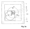
- Fig. 1b shown pressure forces F1, F2 and F3 evenly distributed, since the punch 1 to the actuators 10.1. 10.2 and 10.3 or their pressure transmission rods 17, which are attached to a punch holder 2, which receives the punch 1 centrally, are uniformly spaced.
- the punch holder 2 serves on the one hand the fixation of the punch 1 and uniform force transmission and on the other hand it allows easier replacement of the punch 1, if a new nanostructure 16 must be applied to the substrate 4.
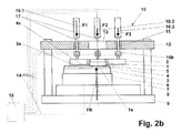
- the device and its components are essentially supported by a lower base plate 9, which is connected via four at the corners of the base plate 9 vertically upwardly projecting connection carrier 7 with a stamp base plate 12 formed.
- Base plate 9 and Stamp base plate 12 are flat and aligned parallel to each other.
- a Justiertischgroundplatte 8 is arranged, which in turn receives an adjustment table 6. This ensures the displacement of the below-described, arranged on the adjusting table 6 components relative to the Justiertischgroundplatte 8 in the X direction, Y direction and in the direction of rotation, i. in a translational and rotational manner.
- a substrate holder 3 Fixed on the adjusting table 6 is a substrate holder 3, which receives the substrate 4 with a possible polymer layer 5, wherein the polymer layer 5 can be applied, for example, via a window 13 in the stamp base plate 12.
- the structure surface 1s s of the punch 1 is arranged and the punch 1 is centrally fixed in the punch holder 2, which in turn by three over the surface of the punch holder 2 on the side facing away from the punch 1 side of the punch holder 2 mounted pressure transmission rods 17 is held.
- the pressure transmission rods 17 are each assigned to one of the three actuators 10. 1, 10. 2 and 10. 3 and guided in a guide 11 in the stamp base plate 12 orthogonally to the stamp base plate 12 or orthogonally to the substrate 4 and the stamp 1.
- load cells 10k are integrated, which measure the tensile and / or compressive forces F1, F2 and F3 and transmitted via connecting lines 14 to the central control device 15.
- the central control device 15 ensures by the measured values obtained or retrieved from the load cells 10k that the stamp face 1s of the stamp 1 is pressed onto the substrate 4 with homogeneous pressure without creating wedge or drift effects.
- the central control device 15 ensures the implementation of the step-and-repeat method, ie the lowering and raising of the punch 1 by the actuator 10, the subsequent displacement of the substrate 4 by the adjusting device 6 to the next, preferably adjacent, field to be printed , wherein the individual fields 21, 22 may consist of several chips 20 (see Fig. 4 ).
- Fig. 5 the stamp 1 is shown with asymmetrical structure 16. Due to the asymmetrical structure 16, the resulting force Fa is moved in the direction of the side with a higher filling factor and thus presses the stamp 1 homogeneously on the polymer layer 5 and the substrate 4.
Landscapes
- Engineering & Computer Science (AREA)
- Chemical & Material Sciences (AREA)
- Nanotechnology (AREA)
- Physics & Mathematics (AREA)
- General Physics & Mathematics (AREA)
- Crystallography & Structural Chemistry (AREA)
- Mechanical Engineering (AREA)
- Theoretical Computer Science (AREA)
- Condensed Matter Physics & Semiconductors (AREA)
- Mathematical Physics (AREA)
- Manufacturing & Machinery (AREA)
- Shaping Of Tube Ends By Bending Or Straightening (AREA)
- Exposure Of Semiconductors, Excluding Electron Or Ion Beam Exposure (AREA)
- Perforating, Stamping-Out Or Severing By Means Other Than Cutting (AREA)
Priority Applications (1)
| Application Number | Priority Date | Filing Date | Title |
|---|---|---|---|
| EP12151884.9A EP2450175B1 (de) | 2007-11-08 | 2007-11-08 | Vorrichtung und Verfahren zum gleichmäßigen Strukturieren von Substraten |
Applications Claiming Priority (2)
| Application Number | Priority Date | Filing Date | Title |
|---|---|---|---|
| EP12151884.9A EP2450175B1 (de) | 2007-11-08 | 2007-11-08 | Vorrichtung und Verfahren zum gleichmäßigen Strukturieren von Substraten |
| EP07021676A EP2058107B1 (de) | 2007-11-08 | 2007-11-08 | Vorrichtung zum gleichmäßigen Strukturieren von Substraten |
Related Parent Applications (1)
| Application Number | Title | Priority Date | Filing Date |
|---|---|---|---|
| EP07021676.7 Division | 2007-11-08 |
Publications (3)
| Publication Number | Publication Date |
|---|---|
| EP2450175A2 EP2450175A2 (de) | 2012-05-09 |
| EP2450175A3 EP2450175A3 (de) | 2012-12-19 |
| EP2450175B1 true EP2450175B1 (de) | 2013-09-11 |
Family
ID=39102908
Family Applications (2)
| Application Number | Title | Priority Date | Filing Date |
|---|---|---|---|
| EP12151884.9A Active EP2450175B1 (de) | 2007-11-08 | 2007-11-08 | Vorrichtung und Verfahren zum gleichmäßigen Strukturieren von Substraten |
| EP07021676A Active EP2058107B1 (de) | 2007-11-08 | 2007-11-08 | Vorrichtung zum gleichmäßigen Strukturieren von Substraten |
Family Applications After (1)
| Application Number | Title | Priority Date | Filing Date |
|---|---|---|---|
| EP07021676A Active EP2058107B1 (de) | 2007-11-08 | 2007-11-08 | Vorrichtung zum gleichmäßigen Strukturieren von Substraten |
Country Status (3)
| Country | Link |
|---|---|
| US (1) | US8763239B2 (ja) |
| EP (2) | EP2450175B1 (ja) |
| JP (1) | JP5590785B2 (ja) |
Families Citing this family (6)
| Publication number | Priority date | Publication date | Assignee | Title |
|---|---|---|---|---|
| WO2014057589A1 (ja) * | 2012-10-12 | 2014-04-17 | アイトリックス株式会社 | 多軸プレス装置及びそれを利用したインプリント装置 |
| JP6116937B2 (ja) * | 2013-02-28 | 2017-04-19 | 公立大学法人大阪府立大学 | パターン形成装置およびそれを用いたパターン形成方法 |
| JP6370539B2 (ja) * | 2013-09-13 | 2018-08-08 | 公立大学法人大阪府立大学 | パターン形成装置およびそれを用いたパターン形成方法 |
| US10495989B2 (en) | 2015-02-12 | 2019-12-03 | Canon Kabushiki Kaisha | Imprint apparatus and method of manufacturing article |
| WO2018041371A1 (de) * | 2016-09-05 | 2018-03-08 | Ev Group E. Thallner Gmbh | Anlage und verfahren zum prägen von mikro- und/oder nanostrukturen |
| CN107144909B (zh) * | 2017-04-06 | 2019-06-07 | 陕西师范大学 | 一种实现非对称传输的单层金纳米结构及其制备方法 |
Family Cites Families (12)
| Publication number | Priority date | Publication date | Assignee | Title |
|---|---|---|---|---|
| CH682108A5 (ja) * | 1991-04-30 | 1993-07-15 | Mettler Toledo Ag | |
| US7432634B2 (en) * | 2000-10-27 | 2008-10-07 | Board Of Regents, University Of Texas System | Remote center compliant flexure device |
| DE20122179U1 (de) | 2000-07-17 | 2004-09-16 | Board of Regents, The University of Texas System, Austin | Vorrichtung zum automatischen Abgeben von Flüssigkeit für Prägelithographieprozesse |
| US7117790B2 (en) * | 2002-01-11 | 2006-10-10 | Massachusetts Institute Of Technology | Microcontact printing |
| CN1732075A (zh) * | 2003-01-15 | 2006-02-08 | 天成科威有限公司 | 图案形成装置、图案形成方法、图案形成系统 |
| WO2004086471A1 (en) * | 2003-03-27 | 2004-10-07 | Korea Institute Of Machinery & Materials | Uv nanoimprint lithography process using elementwise embossed stamp and selectively additive pressurization |
| DE10323365A1 (de) * | 2003-05-21 | 2004-12-09 | Robert Bürkle GmbH | Vorrichtung zur Herstellung geprägter Substrate |
| US7037458B2 (en) * | 2003-10-23 | 2006-05-02 | Intel Corporation | Progressive stamping apparatus and method |
| JP2005268675A (ja) | 2004-03-22 | 2005-09-29 | Canon Inc | 微細パターン形成装置および半導体デバイス製造方法 |
| JP2006116602A (ja) | 2004-09-24 | 2006-05-11 | Bondotekku:Kk | 加圧装置の平行調整方法及び装置 |
| US7517211B2 (en) | 2005-12-21 | 2009-04-14 | Asml Netherlands B.V. | Imprint lithography |
| US7500431B2 (en) * | 2006-01-12 | 2009-03-10 | Tsai-Wei Wu | System, method, and apparatus for membrane, pad, and stamper architecture for uniform base layer and nanoimprinting pressure |
-
2007
- 2007-11-08 EP EP12151884.9A patent/EP2450175B1/de active Active
- 2007-11-08 EP EP07021676A patent/EP2058107B1/de active Active
-
2008
- 2008-11-07 US US12/266,630 patent/US8763239B2/en active Active
- 2008-11-07 JP JP2008286980A patent/JP5590785B2/ja active Active
Also Published As
| Publication number | Publication date |
|---|---|
| JP5590785B2 (ja) | 2014-09-17 |
| US20090151154A1 (en) | 2009-06-18 |
| EP2058107B1 (de) | 2012-08-08 |
| EP2450175A2 (de) | 2012-05-09 |
| US8763239B2 (en) | 2014-07-01 |
| EP2058107A1 (de) | 2009-05-13 |
| JP2009137286A (ja) | 2009-06-25 |
| EP2450175A3 (de) | 2012-12-19 |
Similar Documents
| Publication | Publication Date | Title |
|---|---|---|
| EP2450175B1 (de) | Vorrichtung und Verfahren zum gleichmäßigen Strukturieren von Substraten | |
| DE3805363C2 (ja) | ||
| EP2870510B1 (de) | Strukturstempel, vorrichtung und verfahren zum prägen | |
| WO2010121703A1 (de) | Vorrichtung und verfahren zum trennen eines substrats von einem trägersubstrat | |
| EP2903790A1 (de) | Verfahren und werkzeugeinheit zur einstellung eines stanzspalts | |
| EP0623417A2 (de) | Stanzblech, Verfahren zu seiner Herstellung und Werkzeug zur Durchführung des Verfahrens | |
| DE10052293A1 (de) | Verfahren zum Aufbringen eines Substrats | |
| EP0512267B1 (de) | Kaschiermaschine | |
| EP1927028B1 (de) | Vorrichtung und verfahren zur herstellung einer nanostempelstruktur | |
| EP0473947B1 (de) | Klischeeaufnahme und Folienklischee | |
| WO2014079677A1 (de) | Vorrichtung und verfahren zum bonden | |
| DE19935558B4 (de) | Verfahren zur Erzeugung von Strukturen in einem Substrat im Nanometerbereich | |
| DE102020111830A1 (de) | Gestell für eine Replikationsvorrichtung, Replikationsvorrichtung sowie Verfahren zur Herstellung von nano- und/oder mikrostrukturierten Bauteilen mittels einer Replikationsvorrichtung | |
| EP2659505B1 (de) | Verfahren und vorrichtung zum bonden zweier wafer | |
| DE102008043543A1 (de) | Siebdruckvorrichtung | |
| DE102007019268B4 (de) | Vorrichtung zum Bedrucken und/oder Prägen von Substraten | |
| EP1972996B1 (de) | Verfahren und Vorrichtung zur Erzeugung einer nanostrukturierten Scheibe | |
| DE102014212374B4 (de) | Drucksystem zum Bedrucken von Substraten, Verfahren zum Bedrucken eines Substrats | |
| DE102021003387A1 (de) | Klebefilm | |
| DE102004046629B4 (de) | Verfahren zum Herstellen eines Bauelementes mit einem gedruckten Schaltkreis | |
| EP2286981B1 (de) | Verfahren zum Heissprägen einer Polymerschicht | |
| WO2007025519A2 (de) | Verfahren und vorrichtung zum abformen von strukturen | |
| DE102016202615B4 (de) | Druckplatte | |
| DE19756232C1 (de) | Verstellbares Werkzeug | |
| DE102012219655B4 (de) | Optisches element und herstellung desselben |
Legal Events
| Date | Code | Title | Description |
|---|---|---|---|
| PUAI | Public reference made under article 153(3) epc to a published international application that has entered the european phase |
Free format text: ORIGINAL CODE: 0009012 |
|
| AC | Divisional application: reference to earlier application |
Ref document number: 2058107 Country of ref document: EP Kind code of ref document: P |
|
| AK | Designated contracting states |
Kind code of ref document: A2 Designated state(s): AT DE FR NL |
|
| PUAL | Search report despatched |
Free format text: ORIGINAL CODE: 0009013 |
|
| AK | Designated contracting states |
Kind code of ref document: A3 Designated state(s): AT DE FR NL |
|
| RIC1 | Information provided on ipc code assigned before grant |
Ipc: G03F 7/00 20060101ALN20121115BHEP Ipc: B29C 59/02 20060101AFI20121115BHEP |
|
| 17P | Request for examination filed |
Effective date: 20121128 |
|
| 17Q | First examination report despatched |
Effective date: 20130308 |
|
| RIC1 | Information provided on ipc code assigned before grant |
Ipc: B29C 59/02 20060101AFI20130404BHEP Ipc: G03F 7/00 20060101ALN20130404BHEP |
|
| GRAP | Despatch of communication of intention to grant a patent |
Free format text: ORIGINAL CODE: EPIDOSNIGR1 |
|
| RIC1 | Information provided on ipc code assigned before grant |
Ipc: B29C 59/02 20060101AFI20130502BHEP Ipc: G03F 7/00 20060101ALN20130502BHEP |
|
| INTG | Intention to grant announced |
Effective date: 20130521 |
|
| GRAS | Grant fee paid |
Free format text: ORIGINAL CODE: EPIDOSNIGR3 |
|
| GRAA | (expected) grant |
Free format text: ORIGINAL CODE: 0009210 |
|
| AC | Divisional application: reference to earlier application |
Ref document number: 2058107 Country of ref document: EP Kind code of ref document: P |
|
| AK | Designated contracting states |
Kind code of ref document: B1 Designated state(s): AT DE FR NL |
|
| REG | Reference to a national code |
Ref country code: AT Ref legal event code: REF Ref document number: 631360 Country of ref document: AT Kind code of ref document: T Effective date: 20130915 |
|
| REG | Reference to a national code |
Ref country code: DE Ref legal event code: R096 Ref document number: 502007012290 Country of ref document: DE Effective date: 20131107 |
|
| REG | Reference to a national code |
Ref country code: NL Ref legal event code: T3 |
|
| REG | Reference to a national code |
Ref country code: DE Ref legal event code: R097 Ref document number: 502007012290 Country of ref document: DE |
|
| PLBE | No opposition filed within time limit |
Free format text: ORIGINAL CODE: 0009261 |
|
| STAA | Information on the status of an ep patent application or granted ep patent |
Free format text: STATUS: NO OPPOSITION FILED WITHIN TIME LIMIT |
|
| 26N | No opposition filed |
Effective date: 20140612 |
|
| REG | Reference to a national code |
Ref country code: DE Ref legal event code: R097 Ref document number: 502007012290 Country of ref document: DE Effective date: 20140612 |
|
| REG | Reference to a national code |
Ref country code: FR Ref legal event code: PLFP Year of fee payment: 9 |
|
| REG | Reference to a national code |
Ref country code: FR Ref legal event code: PLFP Year of fee payment: 10 |
|
| REG | Reference to a national code |
Ref country code: FR Ref legal event code: PLFP Year of fee payment: 11 |
|
| PGFP | Annual fee paid to national office [announced via postgrant information from national office to epo] |
Ref country code: NL Payment date: 20231122 Year of fee payment: 17 |
|
| PGFP | Annual fee paid to national office [announced via postgrant information from national office to epo] |
Ref country code: FR Payment date: 20231124 Year of fee payment: 17 Ref country code: DE Payment date: 20231120 Year of fee payment: 17 Ref country code: AT Payment date: 20231117 Year of fee payment: 17 |