EP2442213A1 - Touch screen and touch-type input device - Google Patents
Touch screen and touch-type input device Download PDFInfo
- Publication number
- EP2442213A1 EP2442213A1 EP10786059A EP10786059A EP2442213A1 EP 2442213 A1 EP2442213 A1 EP 2442213A1 EP 10786059 A EP10786059 A EP 10786059A EP 10786059 A EP10786059 A EP 10786059A EP 2442213 A1 EP2442213 A1 EP 2442213A1
- Authority
- EP
- European Patent Office
- Prior art keywords
- electrode
- touch panel
- electrodes
- polylactic acid
- panel according
- Prior art date
- Legal status (The legal status is an assumption and is not a legal conclusion. Google has not performed a legal analysis and makes no representation as to the accuracy of the status listed.)
- Granted
Links
Images





Classifications
-
- G—PHYSICS
- G06—COMPUTING OR CALCULATING; COUNTING
- G06F—ELECTRIC DIGITAL DATA PROCESSING
- G06F3/00—Input arrangements for transferring data to be processed into a form capable of being handled by the computer; Output arrangements for transferring data from processing unit to output unit, e.g. interface arrangements
- G06F3/01—Input arrangements or combined input and output arrangements for interaction between user and computer
- G06F3/03—Arrangements for converting the position or the displacement of a member into a coded form
- G06F3/041—Digitisers, e.g. for touch screens or touch pads, characterised by the transducing means
- G06F3/0414—Digitisers, e.g. for touch screens or touch pads, characterised by the transducing means using force sensing means to determine a position
- G06F3/04144—Digitisers, e.g. for touch screens or touch pads, characterised by the transducing means using force sensing means to determine a position using an array of force sensing means
-
- G—PHYSICS
- G06—COMPUTING OR CALCULATING; COUNTING
- G06F—ELECTRIC DIGITAL DATA PROCESSING
- G06F3/00—Input arrangements for transferring data to be processed into a form capable of being handled by the computer; Output arrangements for transferring data from processing unit to output unit, e.g. interface arrangements
- G06F3/01—Input arrangements or combined input and output arrangements for interaction between user and computer
- G06F3/03—Arrangements for converting the position or the displacement of a member into a coded form
- G06F3/041—Digitisers, e.g. for touch screens or touch pads, characterised by the transducing means
-
- G—PHYSICS
- G06—COMPUTING OR CALCULATING; COUNTING
- G06F—ELECTRIC DIGITAL DATA PROCESSING
- G06F3/00—Input arrangements for transferring data to be processed into a form capable of being handled by the computer; Output arrangements for transferring data from processing unit to output unit, e.g. interface arrangements
- G06F3/01—Input arrangements or combined input and output arrangements for interaction between user and computer
- G06F3/03—Arrangements for converting the position or the displacement of a member into a coded form
- G06F3/041—Digitisers, e.g. for touch screens or touch pads, characterised by the transducing means
- G06F3/0416—Control or interface arrangements specially adapted for digitisers
-
- G—PHYSICS
- G06—COMPUTING OR CALCULATING; COUNTING
- G06F—ELECTRIC DIGITAL DATA PROCESSING
- G06F3/00—Input arrangements for transferring data to be processed into a form capable of being handled by the computer; Output arrangements for transferring data from processing unit to output unit, e.g. interface arrangements
- G06F3/01—Input arrangements or combined input and output arrangements for interaction between user and computer
- G06F3/03—Arrangements for converting the position or the displacement of a member into a coded form
- G06F3/041—Digitisers, e.g. for touch screens or touch pads, characterised by the transducing means
- G06F3/046—Digitisers, e.g. for touch screens or touch pads, characterised by the transducing means by electromagnetic means
Definitions
- the present invention relates to a touch panel and a touch type input device, which are provided on e.g., a display surface and are directly touched with a finger or are touched using an exclusive instrument by the user to enable position information and pressed information on a plane to be inputted at the same time.
- touch type input devices that is, devices adopting a touch panel type has been increased significantly.
- the number of devices which adopt the touch panel type as an input interface has been increased significantly together with the development of the thinned display technique, such as portable phones, portable game machines, and portable music players as well as bank ATMs and ticket vending machines in stations.
- touch panels are mainly of a resistance film type and an electrostatic capacity type, and in addition to these, there are touch panels using an optical type, an electromagnetic induction type, and elastic surface waves with piezoelectric.
- these types are used to detect position information. That is, coordinate information showing in what position on a touch panel the user touches is obtained to execute a designated process based on this information.
- the user touches a button portion displayed on the screen to be able to operate the device as if the user pressed an actual button for operation.
- GUI graphic user interface
- the touch panels have been required to be further varied, so that the request to obtain pressed information together with position information at the same time has been increased recently. That is, if binary information showing in what position on the screen the user touches and how strong the user touches the position is detected, the operability can be further improved.
- Patent Document 1 discloses a technique in which a position detecting device is overlapped with a pressure sensitive sensor to detect position information and pressed information at the same time.
- Patent Document 2 discloses a method which uses a piezoelectric film to obtain pressed information and detects in what portion of a plurality of electrode lines formed in a lattice shape on the piezoelectric film a detected voltage appears to obtain position information.
- the pressure sensitive sensor formed of a piezoelectric film or a pressure sensitive resistor sheet is overlapped onto a typical touch panel performing only position detection.
- the pressure sensitive sensor covers the entire surface of the touch panel.
- the typical touch panel is provided on a certain image display device, and is required to have a high transparency.
- Each of the position detecting touch panel and the pressure sensitive sensor has a plurality of films and electrode layers.
- the films are transparent and transparent electrodes including ITO are used, the entire touch panel can be transparent, but due to the large stacking number, the light transmissivity is lowered.
- the cost is increased. Further, since position information and pressed information are detected separately, the signal process becomes complicated.
- the lattice-shaped fine wire electrodes are formed with respect to the piezoelectric film. Since position information is obtained according to from what lattice-shaped electrode a signal is strongly detected, all the fine wires are required to be connected to the computation processing unit, with the result that the structure becomes significantly complicated.
- an invention according to claim 1 provides a touch panel which includes a molecule oriented polylactic acid film, wherein the polylactic acid film has a first principal plane and a second principal plane formed with electrodes, and the electrode on the first principal plane includes divided electrodes which are electrically divided into at least four.
- the electrode on the second principal plane includes divided electrodes formed so as to be opposite the divided electrodes on the first principal plane, respectively.
- the electrode on the second principal plane includes a uniform ground electrode formed so as to be equally opposite the divided electrodes on the first principal plane.
- the divided electrodes are electrically divided by a plurality of electrode division lines including electrode non-forming portions, and the electrode division lines are formed of straight lines having a predetermined width.
- the electrode division lines cross at one point in the substantially center of the polylactic acid film at a predetermined angle.
- angles formed by the electrode division lines are equal to each other.
- the polylactic acid film is molecule oriented by uniaxial orientation.
- the electrode division lines are formed of a first electrode division line and a second electrode division line, and when an angle formed by the first electrode division line and the orientation direction of the polylactic acid film is ⁇ 1 and an angle formed by the second electrode division line and the orientation direction of the polylactic acid film is ⁇ 2 , the ⁇ 1 and ⁇ 2 satisfy the condition of the following equation 1:
- the first electrode division line is formed in the direction which substantially coincides with the orientation direction of the polylactic acid film, and the second electrode division line is formed in the direction substantially orthogonal to the first electrode division line.
- the electrodes are a transparent electrode having ZnO as a main component.
- An invention according to claim 12 provides a touch type input device having the touch panel according to any one of claims 1 to 11, wherein the respective divided electrodes are connected to a processor which outputs position information and/or pressed information based on voltages detected independently from the divided electrodes.
- the processor includes at least a detection unit which detects respective voltages generated in the divided electrodes, a storage unit which stores a plurality of stored voltage patterns determined previously from respective voltages generated in the divided electrodes and a plurality of pieces of position information corresponding thereto, and a computation unit which creates a detected voltage pattern from the respective voltages detected by the detection unit, compares the detected voltage pattern with the stored voltage patterns, checks the corresponding voltage patterns with a predetermined threshold value to output position information, and computes pressed information from a predetermined voltage similarity ratio of the stored voltage pattern and the detected voltage pattern which have been checked.
- the molecule oriented polylactic acid film has piezoelectric properties, and has a transparency equivalent to acryl. Therefore, according to the present invention, the transparent electrode is provided on the polylactic acid film, so that the touch panel and the touch type input device, which have a very high transparency, can obtain, not only position information, but also pressed information, at the same time, and are inexpensive can be realized.
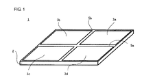
- FIG. 1 is a perspective view showing a first example.
- FIG. 1 enlarges a touch panel 1 which is a main configuration portion of a touch type input device of the present invention.
- the touch panel 1 is connected to a processor and forms the touch type input device of the present invention.
- the processor will be described later.
- the touch panel 1 includes a substrate 2, the substrate 2 having both principal planes formed with electrodes. Electrodes 3a to 3d which are electrically divided by electrode division lines 5a and 5b are formed on a first principal plane of the substrate 2.
- the electrode division lines 5a and 5b pass through the center of a film and cross each other at an angle of substantially 90°.
- the substrate 2 is structured of a polylactic acid film, the polylactic acid film having an orientation axis in the direction which substantially coincides with the longitudinal direction of the electrode division line 5a.
- the respective portions are exaggeratedly shown for explanation, and have dimensions different from the actual dimensions.
- the touch panel is substantially square, which is not limited.
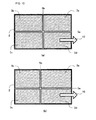
- FIG. 2(a) is a plan view of the touch panel 1.
- An arrow 10 shows the orientation axis direction of the polylactic acid film.
- the arrow 10 is depicted onto the plan view for simple explanation, but such arrow is not depicted onto the actual touch panel 1.
- the electrodes 3a to 3d are electrically connected to a voltage detecting device, which is omitted in this drawing.
- FIG. 2(b) is a plan view showing an example of a second principal plane (back side) of the touch panel 1 shown in FIG. 2(a) , and reversely shows FIG. 2(a) about an electrode division line 50a. Electrodes 30a to 30d divided by the electrode division lines 50a and 50b are formed on the second principal plane so as to be equally opposite the electrodes 3a to 3d on the first principal plane. The electrodes 30a to 30d are opposite the electrodes 3a to 3d in this order. The electrodes 30a to 30d are electrically connected to the voltage detecting device, which is omitted in this drawing.
- FIG. 2(c) is a plan view showing another example of the second principal plane of the touch panel 1 shown in FIG. 2(a) .
- a uniform electrode 4 is formed on the second principal plane so as to be opposite all the electrodes 3a to 3d on the first principal plane.
- the electrode 4 has a ground potential.
- the electrode 4 is electrically connected to the ground of the device equipped with the touch panel 1, which is omitted in this drawing.
- an antireflection film or a protective film is provided, or an antireflection layer or a protective layer is coated, which is omitted in this example.
- the electrode on the second principal plane includes the divided electrodes as shown in FIG. 2(b) or the uniform electrode as shown in FIG. 2(c) with respect to the electrode on the first principal plane is a design matter which can be selected as appropriate at the time of execution. The respective advantages will be described later.
- the electrodes 3a to 3d, the electrodes 30a to 30d, and the electrode 4 include ZnO, ITO, IZO (trademark), an inorganic electrode having these as a main component, or an organic electrode having polythiophene as a main component, and such electrodes can be transparent.
- the electrodes when they are not required to be transparent, they may include a metal.
- Various electrode structuring methods including deposition, sputtering, plating, and foiling are applicable.
- the electrode on the first principal plane and the electrode on the second principal plane are not always required to be of the same type, and different types of electrodes may be used.
- ZnO which enables film formation at room temperature and has a high transparency is preferably used for polylactic acid.
- ZnO has the disadvantage that oxygen deficiency which is a carrier supply source is re-oxidized by reaction with moisture in the atmosphere, thereby increasing resistance.
- a transparent electrode formed using an off-axis type magnetron sputtering method by doping Ga which is an IIIB group element into ZnO at a high density of 7% by weight or more has no practical problems because the activation energy of reaction of H 2 O with ZnO is increased to exhibit an excellent humidity resistance.
- the protective film is provided or the protective layer is coated, so that the possibility that moisture can be directly supplied to ZnO is extremely low.
- the polylactic acid film is a film which is subjected to molecule orientation and then to a thermal treatment. Typically, the polylactic acid film is subjected to uniaxial orientation to enable the polymer main chain to be oriented in the orientation axis direction.
- the polylactic acid is a condensation polymer of lactic acid, and the lactic acid monomer including asymmetric carbon has chirality. Therefore, the polylactic acid includes an L type polylactic acid having a main chain wound counterclockwise, and a D type polylactic acid having a main chain wound clockwise.
- the former will be called PLLA
- the latter will be called PDLA. Since PLLA is typically distributed, hereinafter, the polylactic acid will be represented as PLLA.
- PLLA O and molecules generating permanent dipoles are present in the polymer.
- the large dipole is left in the helical axis direction.
- one reversely oriented molecule chain is present in each crystal unit cell of PLLA, and the dipoles are cancelled in the entire crystal.
- the point group of the PLLA crystal belongs to D 2 , and there are d 14 , d 25 , and d 36 tensor components as piezoelectric strain constants.
- the orientation magnification is preferably about 3 to 8 times.
- the film is subjected to the thermal treatment after orientation to promote crystallization of the extended chain crystal, thereby improving the piezoelectric constant.
- the orientation magnifications of the respective axes are made different from each other, so that the same effect as the uniaxial orientation can be obtained.
- the film is subjected to 8-time orientation in a certain direction as an X axis and is subjected to twice orientation in a Y axis orthogonal to the X axis
- the same piezoelectric constant effect as when the film is subjected to substantially 4-time uniaxial orientation in the X axis direction can be obtained. Since the film which is subjected to simple uniaxial orientation is likely to be torn along the orientation axis direction, the film is subjected to biaxial orientation as described above, so that the strength can be increased to some extent.
- PLLA orientation method In addition to the uniaxial orientation and the biaxial orientation, which have been described here, there is a different PLLA orientation method.
- part of the side chain of the polymer is substituted with a mesogenic group, the properties in which the mesogenic group is oriented by a magnetic field or an electric field are used to orient the main chain itself in a solution, and a solvent is evaporated in this state to obtain an oriented film.
- Orientation is also enabled by applying a high pressure in the thickness direction of the film.
- FIG. 3 is a concept diagram for explaining a modification by the piezoelectric phenomenon of PLLA.
- the axis directed backward from the front of the drawing sheet is a first axis
- the orientation axis shown by the arrow 10 is a third axis.
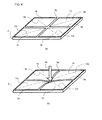
- FIG. 4(a) adds diagonal lines 13a to 13d for explanation to the plan view of the touch panel 1 of FIG. 1 .
- the same figure elements are indicated by the same reference symbols, and the description is omitted.
- FIG. 4(b) shows the state of this deformation.
- An arrow 20 shows the force applied to the center portion of the touch panel 1.
- FIG. 4(b) As understood from FIG. 4(b) , all the diagonal lines 13a to 13d are extended substantially uniformly.
- FIG. 3 is applied to FIG. 4(b) for explanation. That is, the diagonal lines 13a and 13c shown in FIG. 4(b) correspond to the diagonal line 12a of FIG. 3 , and the diagonal lines 13b and 13d shown in FIG. 4(b) correspond to the diagonal line 12b of FIG. 3 .
- the diagonal line 12a is extended to generate an electric field shown by the symbol 11. Therefore, the diagonal lines 13a and 13c are extended to generate plus potentials in the electrodes 3a and 3c.
- the diagonal line 12b is contracted in FIG. 3 , but when the diagonal line 12b is extended, the electric field shown by the symbol 11 is in the reverse direction. Therefore, the diagonal lines 13b and 13d are extended to generate minus potentials in the electrodes 3b and 3d.
- Table 1 shows calculation conditions
- Table 2 shows calculated results.
- the electrode on the back side for this calculation includes the uniform ground electrode.
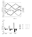
- FIG. 6 is a graph of the results of Table 3.
- Plot points A, B, C, and D shown in the explanatory notes show the voltages generated in the electrodes 3a, 3b, 3c, and 3d, respectively. It is found that the generated voltages are changed substantially smoothly as the pressed positions are changed.
- Table 4 shows results in which the distance from the origin of the pressed coordinates is 12.5 mm and angles formed by the Y axis to the X axis are changed, thereby calculating voltages generated in the electrodes 3a to 3d by the finite element method simulation.
- the calculation conditions are the same as those shown in Table 1.
- FIG. 7 is a graph of the results of Table 4. As in FIG. 6 , plot points A, B, C, and D shown in the explanatory notes show the voltages generated in the electrodes 3a, 3b, 3c, and 3d, respectively. It is found that the generated voltages are changed substantially smoothly as the pressed positions are changed.
- the voltages generated in the electrodes 3a to 3d are changed according to the pressed coordinates.
- a fixed pattern is present in the signs and absolute value magnitudes of the voltages generated in the respective electrodes, and the pattern is analyzed, so that what position on the touch panel 1 is pressed can be obtained as position information.
- the top, middle, and bottom numerical values of the generated voltages in the electrodes in the table correspond to the pressing forces of 0.05 N, 0.1 N, and 0.2 N.
- the generated voltages with the 0.1 N pressing force are substantially twice the generated voltages with the 0.05 N pressing force, and further, the generated voltages with the 0.2 N pressing force are substantially twice the generated voltages with the 0.1 N pressing force.
- FIG. 8 is a bar graph of the generated voltages of the respective electrodes on the coordinate (12.5, 12.5) according to the pressing forces.
- the bar graph itself is a visualized voltage pattern. It is found that the magnitudes of the generated voltages are shifted linearly according to the pressing forces. Therefore, by the method described here, the magnitudes of the generated voltages are totally evaluated, so that pressed information can be obtained. With the above description on balance, the function of obtaining position information and pressed information at the same time will be described anew.
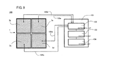
- FIG. 9 explains a touch type input device 100, and is a connection concept diagram of the touch panel 1 and a processor 101.
- the processor 101 includes a detection unit 102, a computation unit 103, and a storage unit 104.
- the detection unit 102 is connected to the electrodes 3a to 3d of the touch panel 1 by connection lines 105a to 105d, respectively.
- the detection unit 102 independently detects voltages generated in the electrodes 3a to 3d when force is applied to the surface of the touch panel 1.
- the storage unit 104 stores, as a voltage pattern, voltages generated in the electrodes 3a to 3d when a predetermined position is pressed by predetermined pressing force.
- the voltage pattern includes, as united information, the signs and magnitudes of the voltages generated in the electrodes 3a to 3d.
- absolute values of the magnitudes of the voltages may be directly stored, and differences from or ratios to the base electrode voltage may be stored. In particular, the storing method described here may not be required to be limited.
- Plural voltage patterns are stored, and the data may be created by a simulation or information when the touch panel 1 is actually pressed may be directly stored.
- the number of voltage patterns to be previously stored is determined as appropriate in view of the coordinate accuracy required of the touch type input device.
- the voltages detected by the detection unit 102 are transmitted to the computation unit 103.
- the computation unit 103 generates a voltage pattern of the voltages detected by the detection unit 102 by the same method as the voltage patterns stored in the storage unit 104.
- the voltage pattern of the detected voltages is generated by the same method as when all the voltage patterns stored in the storage unit 104 are stored at ratios to maximum voltages generated in the respective electrodes.
- the computation unit 103 performs comparison including signs of the created voltage pattern with the voltage patterns stored in the storage unit 104.
- the voltage patterns stored in the storage unit 104 correspond to position information, but pressed information corresponding to position information is discrete to some extent in consideration of the storage capacity limit and the computing speed. Therefore, the voltage patterns which coincide with each other substantially completely cannot be obtained.
- the computation unit 103 reads the voltage pattern at the point located around the position from the storage unit 104, and generates the voltage values of the electrodes generating the maximum voltages at the position by linear interpolation. Maximum ratios of the generated voltage values to the detected voltages are calculated, and then, the predetermined pressing force stored in the storage unit 104 is multiplied by each of the ratios, so that actual pressing force can be calculated.
- the method of determining position information and pressed information described here is not limited.
- the electrode on the back side opposite the electrodes 3a to 3d includes the uniform ground electrode 4 as shown in FIG. 2(c) .
- the uniform ground electrode 4 has a simple structure and does not require patterning, so that the ground electrode 4 can be formed inexpensively.
- the ground electrode 4 has a back side without any electrode non-forming portions, so that when the back side is perspectively seen from the front side, the pattern of the electrode is hard to be recognized.
- the touch type input device can use the touch panel 1 having a very simple structure to output position information and pressed information at the same time.
- PLLA used as the material of the substrate 2 of the touch panel 1 is a condensation polymer of lactic acid.
- lactic acid is made from starch with corns as a raw material by using the force of microorganisms. Therefore, PLLA does not use a fossil fuel as a material, so that carbon dioxide in the air cannot be increased at the time of disposal.
- PLLA has a much smaller carbon dioxide exhaust amount at the time of manufacture than other polymers. Further, since PLLA has a biodegradability characteristic, the device having an extremely low environmental load can be provided.
- the position information detection and the pressed information detection by the method described here can also be achieved by using other piezoelectric polymers such as PVDF as the substrate 2 in the same electrode structure.
- PVDF piezoelectric polymers
- all the voltages generated from the respective electrodes have a plus potential or a minus potential. This is determined depending on the poling direction of PVDF.
- PLLA in which there is a polarity in the voltages generated in the respective electrodes has a larger information amount to be obtained than PVDF.
- the piezoelectric properties of PLLA which are caused due to the molecular orientation occurring from the orientation and the thermal treatment, are held semi-permanently.
- PVDF which is an opaque white polymer is made thinner, it becomes transparent, but it has a lower transparency than PLLA, so that in view of this point, PLLA is very excellent as the touch panel.
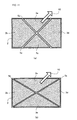
- FIG. 10(a) shows another embodiment of the first example shown in FIGS. 1 to 2(c) .
- FIG. 10(a) corresponds to FIG. 2(a)
- the back sides corresponding to FIGS. 2B and 2(c) are not shown.
- the following examples and modification examples are also not shown when the electrode on the back side includes the uniform electrode. Components having the same functions are indicated by the same reference symbols, and the description is omitted.
- the substrate 2 is rectangular.
- the touch panel is often provided on the surface of a display, and the number of rectangular displays is typically overwhelmingly large, so that the touch panel essentially has the same shape.
- the touch panel having such shape can function as in the case described in the first example.
- FIG. 10B is a modification example of the example shown in FIG. 10(a) .
- the electrode division lines 5a and 5b do not pass through the center of the substrate 2, and a cross point thereof is in the position shifted from the center portion of the substrate 2.
- the cross point of the electrode division lines 5a and 5b may be shifted from the center of the substrate 2 by a predetermined amount.
- the cross point of the electrode division lines 5a and 5b is preferably set near the portion in which position detection is necessary most frequently.
- the shift amount may be set as appropriate according to the design by checking the detection accuracy.
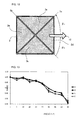
- FIG. 11(a) shows another embodiment of the second example. Components having the same functions are indicated by the same reference symbols, and the description is omitted.
- the substrate 2 is rectangular.
- PLLA of the substrate 2 is cut out so that the orientation axis is at an angle of 45° to the side of the outer frame of the substrate 2.
- PLLA is extended and contracted in the direction at an angle of 45° to the orientation axis by voltage application. Therefore, to efficiently perform voltage detection, as shown in FIG. 11(a) , preferably, one of the electrode division lines 5a and 5b is directed in the same direction as the orientation axis, and the other is directed in the direction at an angle of 90° to the orientation axis.
- the cross point of the electrode division lines 5a and 5b may also be shifted from the center of the substrate 2.
- FIG. 11B is a modification example of the example shown in FIG. 11(a) .
- the direction of the orientation axis of PLLA of the substrate 2 is the same as FIG. 11(a) , but both the electrode division lines 5a and 5b are not along the direction of the orientation axis, and are formed along the diagonal lines of the substrate 2.
- the modification example in FIG. 11B can have a slightly lower detected voltage than FIG. 11(a) , but can be practically used without any problems.
- a plus potential is generated in the portion along the electrode division line 5a and a minus potential having a substantially equal absolute value is generated in the portion along the electrode division line 5b. Therefore, in the electrodes 3a to 3d, the voltages are substantially canceled. Therefore, when only two electrode division lines are used, preferably, 0° ⁇ ⁇ 1 ⁇ 45° and -90° ⁇ ⁇ 2 ⁇ -45°.
- FIG. 13 is a graph showing results in which in the model shown in FIG. 12 , voltages generated when the center portion of the substrate 2 is pressed are calculated by the infinite element method simulation.
- ⁇ 2 ⁇ 1 - 90°.
- ⁇ 1 when ⁇ 1 is practically set as advantageously as possible, preferably, ⁇ 1 ⁇ 25°.
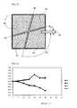
- FIG. 14 shows a modification example of FIG. 2 and a plan view when the electrode division line 5a is rotated ⁇ 1 from the orientation axis and the electrode division line 5b is rotated ⁇ 2 from the orientation axis.
- FIG. 15 is a graph showing results in which in the model shown in FIG. 14 , voltages generated when the center portion of the substrate 2 is pressed are calculated by the finite element method simulation.
- the decreasing rate of the voltages in the divided electrodes 3b and 3d is larger than the increasing rate of the voltages in the divided electrodes 3a and 3c.
- the range of ⁇ 1 is 0° ⁇ ⁇ 1 ⁇ 12°.
- the range of ⁇ 1 is -25° ⁇ ⁇ 1 ⁇ 25°, so that the voltage of 80% or more of the maximum value of the generated voltage can be detected.
- the decreasing amount of the voltage with respect to the maximum voltage is 80%, but this is an amount which can be typically considered by those skilled in the art, and the decreasing amount may be considered to be a smaller value than this when there are no problems in the actual use, and the values of ⁇ 1 and ⁇ 2 to be taken may be increased as appropriate.
- FIG. 16 is a plan view showing another embodiment of the first to third examples. Components having the same functions as the above examples are indicated by the same reference symbols, and the description is omitted.
- the electrode formed on the principal plane of the substrate 2 is divided into eight divided electrodes 3a to 3h by the electrode division lines 5a to 5d.
- the operation principle of this example is equal to that described in the first example.
- the number of voltage detection elements is increased, so that the voltage pattern with respect to position information can be formed more finely. Thereby, both position information and pressed information can increase the accuracy.
- All the electrode division lines 5a to 5d cross in the center portion of the substrate 2 in this example, but are not always required to cross in the center portion, as described in the second example.
- the electrode division lines are in the direction which coincides with the orientation axis and are orthogonal thereto, or other electrode division lines are set at angles as described in the third example so that the angles formed by the electrode division lines are equalized, or other electrode division lines are provided so that the divided electrodes divided by the electrode division lines are divided by an equal area to the extent possible.
- FIG. 17 is a plan view showing a further embodiment of the first to fourth examples. Components having the same functions as the above examples are indicated by the same reference symbols, and the description is omitted.
- Irregular shaped electrodes 3a to 3d and electrode non-forming regions 8a to 8g are formed on the principal plane of the substrate 2.
- the electrodes 3a to 3d are electrically divided by the electrode non-forming regions, and can perform the same operation as other examples.
- Centerlines 31a to 31d are the centerlines showing the longer axis of the electrodes. As shown here, the electrodes are not always required to cover the entire principal plane of the substrate 2. In the electrode structure shown in FIG.
- each of the electrodes 3a to 3d is in the direction at one of 45° and -45° to the orientation axis shown by the arrow 10, that is, each of the centerlines 31a to 31d is in the direction at one of 45° and -45° to the orientation axis shown by the arrow 10, so that the possibility that only electric charges of the same sign can occur in the island of one electrode by pressing becomes extremely high. Therefore, the possibility that the voltages can be cancelled by reverse electric charges becomes very low.
- the electrodes are not always required to be axisymmetric with respect to the centerlines of the substrate 2.
- the methods shown in the second and fourth examples are combined to enable various electrode shapes to be set.
- the edges of the electrodes are not always required to be a straight line, and may be a curved line. These are matters determined, as need, according to the design.
- FIG. 18 is a plan view showing an embodiment having an electrode shape concept different from the first to fifth examples. Electrodes 9a to 9t are formed in a check pattern on the principal plane of the substrate 2. All the extraction electrodes of the electrodes 9a to 9t are not shown. Pressing force is applied to a predetermined position on the substrate 2, so that voltages according to the pressed coordinate and the pressing force are generated in the electrodes 9a to 9t. Since a plurality of electrodes are present, a detailed voltage pattern can be obtained, so that the improvement of the position detection accuracy can be expected. Since the number of voltages obtained is large to increase the load of the analyzing process, the computing process may be executed by narrowing down the electrodes which output voltages above a specified threshold value.
- the electrodes When the number of divided electrodes is increased as in the example shown here, the consideration of the direction with the orientation axis becomes meaningless, so that free arrangement is enabled.
- the example in which the electrodes are arranged in the check pattern but the electrodes may be arranged in a matrix sectioned by lattice-shaped electrode division lines.
- the lattice-shaped electrode division lines at this time more preferably, one of the vertical axis and the horizontal axis is along the orientation axis and the other is at substantially 90° with respect to the one axis.
- the shape of the electrodes is not limited to be square and rectangular, and may be polygonal, circular, elliptical, and irregular shape.
- the same position information and pressed information obtaining method as the first example is used.
- the electrode division number is a design matter to be determined in consideration of the signal processing ability.
- the electrode on the back side in the second to sixth examples may include the divided electrodes opposite the electrodes shown in the plan views in the examples, and may form a uniform ground electrode. This is a design matter which can be selected as appropriate for execution.
- the number of divided electrodes is reduced to less than four will be described here.
- the electrode formed on the principal plane is divided into two, the detected voltage pattern is significantly deteriorated, with the result that the detection of position information can be rough.
- Various accuracies are required of the touch panel according to devices to which the touch panel is applied, so that among the devices, the devices requiring only low accuracy can reduce the electrode division number.
- the electrode division number may be about two or three.
- FIG. 19 is a concept diagram for explaining a still further embodiment.
- the PLLA films 201a and 201b are stacked.
- the PLLA films 201a and 201b are formed with electrodes as described in the above examples.
- the adhesive interface portion of the PLLA films 201a and 201b is on the ground electrode side of both films, which is simple and preferable in structure. In this drawing, the electrodes and the adhesive are omitted.
- FIG. 15 shows a cross section of the portion to which a stress shown by the arrow 20 is applied, and the substrate 2 is flexed by this stress. With the interface as a neutral surface, a compressive stress occurs in the PLLA film 201a, and a tension stress occurs in the PLLA film 201b.
- the PLLA films 201a and 201b When the four divided electrodes are formed on the PLLA films 201a and 201b, voltages according to the stresses are generated in the electrodes. Since the PLLA films 201a and 201b can form a more detailed voltage pattern than one layer, position information and pressed information can both increase the accuracy. Also, when the angle formed by the orientation directions of the PLLA films 201a and 201b is 90°, molecular chains are perspectively formed in a lattice shape, so that the touch panel can be strong. However, the angle between the orientation axes is not necessary 90°, and when it is larger than 0°, the increase of the strength can be expected. Also, the stacking number is not limited to two, and may be increased, as needed.
- the touch panels shown in the first to fifth examples only show typical examples of the present invention.
- the results calculated by the finite element method simulation are changed according to film thickness, other electric constants, the types, thickness, and hardness of protective films to be stacked, and the numerical values shown here are not limited. Therefore, the distribution, detection method, and computing method of detected voltages should be determined according to the design for execution.
- the touch panel and the touch type input device of the present invention can obtain position information and pressed information at the same time by a simple structure, have a high transparency, and can be inexpensive. Further, a very great merit that no load is given to an environment at the time of disposal can be obtained, so that there is an industrial applicability.
Landscapes
- Engineering & Computer Science (AREA)
- Theoretical Computer Science (AREA)
- General Engineering & Computer Science (AREA)
- Physics & Mathematics (AREA)
- General Physics & Mathematics (AREA)
- Human Computer Interaction (AREA)
- Electromagnetism (AREA)
- Position Input By Displaying (AREA)
- Manufacture Of Macromolecular Shaped Articles (AREA)
- Laminated Bodies (AREA)
- Force Measurement Appropriate To Specific Purposes (AREA)
- Biological Depolymerization Polymers (AREA)
- Compositions Of Macromolecular Compounds (AREA)
Abstract
Description
- The present invention relates to a touch panel and a touch type input device, which are provided on e.g., a display surface and are directly touched with a finger or are touched using an exclusive instrument by the user to enable position information and pressed information on a plane to be inputted at the same time.
- In recent years, the number of touch type input devices, that is, devices adopting a touch panel type has been increased significantly. The number of devices which adopt the touch panel type as an input interface has been increased significantly together with the development of the thinned display technique, such as portable phones, portable game machines, and portable music players as well as bank ATMs and ticket vending machines in stations.
- Currently used touch panels are mainly of a resistance film type and an electrostatic capacity type, and in addition to these, there are touch panels using an optical type, an electromagnetic induction type, and elastic surface waves with piezoelectric. Typically, these types are used to detect position information. That is, coordinate information showing in what position on a touch panel the user touches is obtained to execute a designated process based on this information. As typified by bank ATMs, the user touches a button portion displayed on the screen to be able to operate the device as if the user pressed an actual button for operation. With the recent development of the graphic user interface (GUI) process technique, there are also devices in which the user can touch the screen to scroll displayed images or can directly control a graphically displayed slide switch with a finger.
- The touch panels have been required to be further varied, so that the request to obtain pressed information together with position information at the same time has been increased recently. That is, if binary information showing in what position on the screen the user touches and how strong the user touches the position is detected, the operability can be further improved.
- As a technique in connection with this,
Patent Document 1 discloses a technique in which a position detecting device is overlapped with a pressure sensitive sensor to detect position information and pressed information at the same time. - Also,
Patent Document 2 discloses a method which uses a piezoelectric film to obtain pressed information and detects in what portion of a plurality of electrode lines formed in a lattice shape on the piezoelectric film a detected voltage appears to obtain position information. -
- Patent Document 1: Japanese Patent Application Laid-Open (JP-A) No.
5-61592 - Patent Document 2: Japanese Patent Application Laid-Open (JP-A) No.
2006-163618 - In the touch panel described in
Patent Document 1, the pressure sensitive sensor formed of a piezoelectric film or a pressure sensitive resistor sheet is overlapped onto a typical touch panel performing only position detection. The pressure sensitive sensor covers the entire surface of the touch panel. - In general, the typical touch panel is provided on a certain image display device, and is required to have a high transparency. Each of the position detecting touch panel and the pressure sensitive sensor has a plurality of films and electrode layers. When the films are transparent and transparent electrodes including ITO are used, the entire touch panel can be transparent, but due to the large stacking number, the light transmissivity is lowered. In addition, since a plurality of components and processes are necessary, the cost is increased. Further, since position information and pressed information are detected separately, the signal process becomes complicated.
- Also, in the touch panel described in
Patent Document 2, to detect position information and pressed information at the same time, the lattice-shaped fine wire electrodes are formed with respect to the piezoelectric film. Since position information is obtained according to from what lattice-shaped electrode a signal is strongly detected, all the fine wires are required to be connected to the computation processing unit, with the result that the structure becomes significantly complicated. - To address the above problems, an invention according to
claim 1 provides a touch panel which includes a molecule oriented polylactic acid film, wherein the polylactic acid film has a first principal plane and a second principal plane formed with electrodes, and the electrode on the first principal plane includes divided electrodes which are electrically divided into at least four. - In an invention according to
claim 2, in the touch panel according toclaim 1, the electrode on the second principal plane includes divided electrodes formed so as to be opposite the divided electrodes on the first principal plane, respectively. - In an invention according to claim 3, in the touch panel according to
claim 1, the electrode on the second principal plane includes a uniform ground electrode formed so as to be equally opposite the divided electrodes on the first principal plane. - In an invention according to claim 4, in the touch panel according to any one of
claims 1 to 3, the divided electrodes are electrically divided by a plurality of electrode division lines including electrode non-forming portions, and the electrode division lines are formed of straight lines having a predetermined width. - In an invention according to
claim 5, in the touch panel according to claim 4, the electrode division lines cross at one point in the substantially center of the polylactic acid film at a predetermined angle. - In an invention according to claim 6, in the touch panel according to
claim 5, angles formed by the electrode division lines are equal to each other. - In an invention according to claim 7, in the touch panel according to any one of
claims 1 to 6, the polylactic acid film is molecule oriented by uniaxial orientation. - In an invention according to claim 8, in the touch panel according to claim 7, the electrode division lines are formed of a first electrode division line and a second electrode division line, and when an angle formed by the first electrode division line and the orientation direction of the polylactic acid film is θ1 and an angle formed by the second electrode division line and the orientation direction of the polylactic acid film is θ2, the θ1 and θ2 satisfy the condition of the following equation 1:
-

- In an invention according to claim 9, in the touch panel according to claim 8, the first electrode division line is formed in the direction which substantially coincides with the orientation direction of the polylactic acid film, and the second electrode division line is formed in the direction substantially orthogonal to the first electrode division line.
- In an invention according to
claim 10, in the touch panel according to any one ofclaims 1 to 9, the electrodes are a transparent electrode having ZnO as a main component. - In an invention according to
claim 11, in the touch panel according to any one ofclaims 1 to 10, two or more polylactic acid films are stacked. - An invention according to claim 12 provides a touch type input device having the touch panel according to any one of
claims 1 to 11, wherein the respective divided electrodes are connected to a processor which outputs position information and/or pressed information based on voltages detected independently from the divided electrodes. - In an invention according to claim 13, in the touch type input device according to claim 12, the processor includes at least a detection unit which detects respective voltages generated in the divided electrodes, a storage unit which stores a plurality of stored voltage patterns determined previously from respective voltages generated in the divided electrodes and a plurality of pieces of position information corresponding thereto, and a computation unit which creates a detected voltage pattern from the respective voltages detected by the detection unit, compares the detected voltage pattern with the stored voltage patterns, checks the corresponding voltage patterns with a predetermined threshold value to output position information, and computes pressed information from a predetermined voltage similarity ratio of the stored voltage pattern and the detected voltage pattern which have been checked.
- The molecule oriented polylactic acid film has piezoelectric properties, and has a transparency equivalent to acryl. Therefore, according to the present invention, the transparent electrode is provided on the polylactic acid film, so that the touch panel and the touch type input device, which have a very high transparency, can obtain, not only position information, but also pressed information, at the same time, and are inexpensive can be realized.
-
-
FIG. 1 is a perspective view showing a basic structure of a touch panel of the present invention. -
FIG. 2(a) is a plan view showing a front side electrode structure of the touch panel of the present invention,FIG. 2(b) is a plan view showing a back side electrode structure of the touch panel of the present invention, andFIG. 2(c) is a plan view showing another back side electrode structure of the touch panel of the present invention. -
FIG. 3 is an explanatory view for explaining a modification by the piezoelectric phenomenon of polylactic acid. -
FIG. 4 is a perspective view for explaining a basic operation of the present invention. -
FIG. 5 is a plan view which defines coordinates for explaining the basic operation of the present invention. -
FIG. 6 is a graph showing the relation between pressed information and voltages generated from the respective electrodes when pressing force is applied along diagonal lines of the touch panel of the present invention. -
FIG. 7 is a graph showing the relation between pressed information and voltages generated from the respective electrodes when pressing force is applied to positions at predetermined angles to an X axis at an equal distance from the center portion of the touch panel of the present invention. -
FIG. 8 is a graph of patterns of voltages generated from the respective electrodes when predetermined pressing forces are applied to predetermined positions of the touch panel of the present invention to change the pressing forces. -
FIG. 9 is a block diagram of a touch type input device of the present invention. -
FIG. 10(a) is a plan view showing a second example of the present invention, andFIG. 10(b) is a plan view showing a modification example of the second example of the present invention. -
FIG. 11(a) is a plan view showing a third example of the present invention, andFIG. 11(b) is a plan view showing a modification example of the third example of the present invention. -
FIG. 12 is a first explanatory view for explaining the third example of the present invention. -
FIG. 13 is a first graph showing the relation between directions formed by electrode division lines and an orientation axis and voltages generated in the respective electrodes in the touch panel shown in the third example of the present invention. -
FIG. 14 is a second explanatory view for explaining the third example of the present invention. -
FIG. 15 is a second graph showing the relation between directions formed by electrode division lines and an orientation axis and voltages generated in the respective electrodes in the touch panel shown in the third example of the present invention. -
FIG. 16 is a plan view showing a fourth example of the present invention. -
FIG. 17 is a plan view showing a fifth example of the present invention. -
FIG. 18 is a plan view showing a sixth example of the present invention. -
FIG. 19 is an explanatory view for explaining a seventh example of the present invention. -
FIG. 1 is a perspective view showing a first example.FIG. 1 enlarges atouch panel 1 which is a main configuration portion of a touch type input device of the present invention. Thetouch panel 1 is connected to a processor and forms the touch type input device of the present invention. The processor will be described later. Thetouch panel 1 includes asubstrate 2, thesubstrate 2 having both principal planes formed with electrodes.
Electrodes 3a to 3d which are electrically divided byelectrode division lines substrate 2. Theelectrode division lines substrate 2 is structured of a polylactic acid film, the polylactic acid film having an orientation axis in the direction which substantially coincides with the longitudinal direction of theelectrode division line 5a. In the drawing, the respective portions are exaggeratedly shown for explanation, and have dimensions different from the actual dimensions.
In addition, here, the touch panel is substantially square, which is not limited. -
FIG. 2(a) is a plan view of thetouch panel 1. Anarrow 10 shows the orientation axis direction of the polylactic acid film. Thearrow 10 is depicted onto the plan view for simple explanation, but such arrow is not depicted onto theactual touch panel 1. Theelectrodes 3a to 3d are electrically connected to a voltage detecting device, which is omitted in this drawing. -
FIG. 2(b) is a plan view showing an example of a second principal plane (back side) of thetouch panel 1 shown inFIG. 2(a) , and reversely showsFIG. 2(a) about anelectrode division line 50a.Electrodes 30a to 30d divided by theelectrode division lines electrodes 3a to 3d on the first principal plane. Theelectrodes 30a to 30d are opposite theelectrodes 3a to 3d in this order. Theelectrodes 30a to 30d are electrically connected to the voltage detecting device, which is omitted in this drawing. -
FIG. 2(c) is a plan view showing another example of the second principal plane of thetouch panel 1 shown inFIG. 2(a) . A uniform electrode 4 is formed on the second principal plane so as to be opposite all theelectrodes 3a to 3d on the first principal plane. The electrode 4 has a ground potential. The electrode 4 is electrically connected to the ground of the device equipped with thetouch panel 1, which is omitted in this drawing. - In addition, typically, on the front side and the back side of the touch panel, an antireflection film or a protective film is provided, or an antireflection layer or a protective layer is coated, which is omitted in this example.
- Whether the electrode on the second principal plane includes the divided electrodes as shown in
FIG. 2(b) or the uniform electrode as shown inFIG. 2(c) with respect to the electrode on the first principal plane is a design matter which can be selected as appropriate at the time of execution. The respective advantages will be described later. - The
electrodes 3a to 3d, theelectrodes 30a to 30d, and the electrode 4 include ZnO, ITO, IZO (trademark), an inorganic electrode having these as a main component, or an organic electrode having polythiophene as a main component, and such electrodes can be transparent. However, when the electrodes are not required to be transparent, they may include a metal. Various electrode structuring methods including deposition, sputtering, plating, and foiling are applicable. In addition, the electrode on the first principal plane and the electrode on the second principal plane are not always required to be of the same type, and different types of electrodes may be used. - In particular, ZnO which enables film formation at room temperature and has a high transparency is preferably used for polylactic acid. Originally, ZnO has the disadvantage that oxygen deficiency which is a carrier supply source is re-oxidized by reaction with moisture in the atmosphere, thereby increasing resistance. A transparent electrode formed using an off-axis type magnetron sputtering method by doping Ga which is an IIIB group element into ZnO at a high density of 7% by weight or more has no practical problems because the activation energy of reaction of H2O with ZnO is increased to exhibit an excellent humidity resistance. In addition, in the actual use, in general, on the
touch panel 1, the protective film is provided or the protective layer is coated, so that the possibility that moisture can be directly supplied to ZnO is extremely low. - Here, the piezoelectric properties of the polylactic acid will be described. The polylactic acid film is a film which is subjected to molecule orientation and then to a thermal treatment. Typically, the polylactic acid film is subjected to uniaxial orientation to enable the polymer main chain to be oriented in the orientation axis direction. The polylactic acid is a condensation polymer of lactic acid, and the lactic acid monomer including asymmetric carbon has chirality. Therefore, the polylactic acid includes an L type polylactic acid having a main chain wound counterclockwise, and a D type polylactic acid having a main chain wound clockwise. The former will be called PLLA, and the latter will be called PDLA. Since PLLA is typically distributed, hereinafter, the polylactic acid will be represented as PLLA.
- In PLLA, C = O and molecules generating permanent dipoles are present in the polymer. When the sum of the dipoles with respect to one molecular chain is calculated, the large dipole is left in the helical axis direction. On the other hand, one reversely oriented molecule chain is present in each crystal unit cell of PLLA, and the dipoles are cancelled in the entire crystal. The point group of the PLLA crystal belongs to D2, and there are d14, d25, and d36 tensor components as piezoelectric strain constants.
- It is known that when the film is uniaxially oriented, the symmetry of part thereof is collapsed due to the influence of the polymer helical structure to exhibit shear piezoelectric properties. The components observed as the piezoelectric strain constants are d14 and d25, and the component d36 is cancelled due to the presence of a vertical mirror surface.
- The orientation magnification is preferably about 3 to 8 times. The film is subjected to the thermal treatment after orientation to promote crystallization of the extended chain crystal, thereby improving the piezoelectric constant. In the case of biaxial orientation, the orientation magnifications of the respective axes are made different from each other, so that the same effect as the uniaxial orientation can be obtained. For example, when the film is subjected to 8-time orientation in a certain direction as an X axis and is subjected to twice orientation in a Y axis orthogonal to the X axis, the same piezoelectric constant effect as when the film is subjected to substantially 4-time uniaxial orientation in the X axis direction can be obtained. Since the film which is subjected to simple uniaxial orientation is likely to be torn along the orientation axis direction, the film is subjected to biaxial orientation as described above, so that the strength can be increased to some extent.
- In addition to the uniaxial orientation and the biaxial orientation, which have been described here, there is a different PLLA orientation method. For example, part of the side chain of the polymer is substituted with a mesogenic group, the properties in which the mesogenic group is oriented by a magnetic field or an electric field are used to orient the main chain itself in a solution, and a solvent is evaporated in this state to obtain an oriented film. Orientation is also enabled by applying a high pressure in the thickness direction of the film.
-
FIG. 3 is a concept diagram for explaining a modification by the piezoelectric phenomenon of PLLA. The axis directed backward from the front of the drawing sheet is a first axis, and the orientation axis shown by thearrow 10 is a third axis. When an electric field is applied in the first axis direction to aPLLA film 2a, thePLLA film 2a is deformed so as to be extended in the direction which substantially coincides with adiagonal line 12a and to be contracted in the direction which substantially coincides with adiagonal line 12b due to the influence of shear elasticity of d14. Finally, the PLLA film is deformed into a shape shown by 2b. Asymbol 11 shows the direction of the electric field, and shows that the electric field is present backward from the front of the drawing sheet. A deformation amount is exaggeratedly expressed. - It is known that in d14 of PLLA, a value as much as 10 to 20 pC/N can be obtained by arranging the orientation condition, the thermal treatment condition, and the additive mixing condition.
- In the film having such piezoelectric properties, when the electric field is applied to cause deformation, as described above, and on the contrary, when deformation is given, a voltage occurs. As an index discussing such properties, there is a piezoelectric stress constant (g constant). In PLLA, g14 reaches 300 to 500 × 10-3 Vm/N, which is much larger than PVDF (g31 = 216 × 10-3 Vm/N) and PZT (g31 = 11 × 10-3 Vm/N). Therefore, PLLA is very preferable as sensing application.
- Next, a method of obtaining position information and pressed information using g14 of PLLA will be described.
-
FIG. 4(a) addsdiagonal lines 13a to 13d for explanation to the plan view of thetouch panel 1 ofFIG. 1 . The same figure elements are indicated by the same reference symbols, and the description is omitted. When downward force is applied to the center portion of thetouch panel 1, the center portion of thetouch panel 1 is flexed according thereto. The state of this deformation is shown inFIG. 4(b) . Anarrow 20 shows the force applied to the center portion of thetouch panel 1. - As understood from
FIG. 4(b) , all thediagonal lines 13a to 13d are extended substantially uniformly.FIG. 3 is applied toFIG. 4(b) for explanation. That is, thediagonal lines FIG. 4(b) correspond to thediagonal line 12a ofFIG. 3 , and thediagonal lines FIG. 4(b) correspond to thediagonal line 12b ofFIG. 3 . - When the explanation with
FIG. 3 is considered reversely, thediagonal line 12a is extended to generate an electric field shown by thesymbol 11. Therefore, thediagonal lines electrodes diagonal line 12b is contracted inFIG. 3 , but when thediagonal line 12b is extended, the electric field shown by thesymbol 11 is in the reverse direction. Therefore, thediagonal lines electrodes - Next, results in which a finite element method simulation is performed by using the model shown in
FIG. 4(b) are shown. Table 1 shows calculation conditions, and Table 2 shows calculated results. As shown inFIG. 2(c) , the electrode on the back side for this calculation includes the uniform ground electrode. -
[Table 1] Item Conditions Film size 50 × 50 mm Film thickness 75 µm Electrode Only boundary conditions Width of electrode division line 0.5 mm Piezoelectric strain constant (d14) 2 OpC/N Pressed spot size Circle having a radius of 2 mm Pressing force 0.1 N -
[Table 2] Electrode 3aElectrode 3bElectrode 3cElectrode 3d Generated voltage (mV) 78.13 -77.76 76.32 -79.39 - As described above, plus potentials are generated in the
electrodes electrodes - Next, there are shown results in which coordinate axes are set so that the center portion of the
touch panel 1 is an origin, as shown inFIG. 5 and voltages generated when various positions are pressed are calculated by using the finite element method simulation. The calculation conditions are the same as those shown in Table 1. Table 3 shows voltages generated when positions along thediagonal line 13a are pressed. The unit of the numerical values in the table is mV. -
[Table 3] Pressed coordinate (X, Y) Electrode 3aElectrode 3bElectrode 3cElectrode 3d (0, 0) 78.13 -77.76 76.32 -79.39 (2.5, 2.5) 81.56 -64.00 42.26 -58.51 (5.0, 5.0) 85.25 -56.84 25.55 -43.18 (7.5, 7.5) 79.91 -50.61 9.71 -32.61 (10.0, 10.0) 71.60 -42.06 -4.73 -20.16 (12.5, 12.5) 60.59 -33.80 -7.92 -16.99 (15.0, 15.0) 41.58 -22.89 -10.55 -7.99 (17.5, 17.5) 22.02 -11.44 -9.42 -3.41 (20.0, 20.0) 6.27 -3.31 -2.73 -0.57 -
FIG. 6 is a graph of the results of Table 3. Plot points A, B, C, and D shown in the explanatory notes show the voltages generated in theelectrodes - Table 4 shows results in which the distance from the origin of the pressed coordinates is 12.5 mm and angles formed by the Y axis to the X axis are changed, thereby calculating voltages generated in the
electrodes 3a to 3d by the finite element method simulation. The calculation conditions are the same as those shown in Table 1. -
[Table 4] Pressed coordinate (r, θ) Electrode 3aElectrode 3bElectrode 3cElectrode 3d (12.5, 0) 42.58 -15.54 20.47 -51.70 (12.5, 30) 71.04 -36.19 6.24 -34.50 (12.5, 60) 85.46 -60.83 1.27 -25.92 (12.5, 90) 69.58 -69.53 9.28 -12.21 (12.5, 120) 59.16 -77.27 24.81 -2.84 (12.5, 150) 41.53 -73.42 45.54 -4.84 (12.5, 180) 23.84 -48.71 55.84 -17.82 (12.5, 210) 9.34 -32.78 69.85 -38.62 (12.5, 240) 5.05 -23.17 82.44 -54.39 (12.5, 270) 13.95 -7.70 70.75 -72.37 (12.5, 300) 29.24 1.44 54.52 -82.55 (12.5, 330) 48.78 -1.78 37.58 -77.54 -
FIG. 7 is a graph of the results of Table 4. As inFIG. 6 , plot points A, B, C, and D shown in the explanatory notes show the voltages generated in theelectrodes - As shown in Tables 2 to 4, the voltages generated in the
electrodes 3a to 3d are changed according to the pressed coordinates. A fixed pattern is present in the signs and absolute value magnitudes of the voltages generated in the respective electrodes, and the pattern is analyzed, so that what position on thetouch panel 1 is pressed can be obtained as position information. - Next, pressing force detection method will be described. Table 5 shows results in which generated voltages obtained when pressing forces are 0.05 N, 0.1 N, and 0.2 N with respect to the respective positions of (X, Y) = (12.5, 12.5), (-12.5, 12.5), (-12.5, -12.5), and (12.5, -12.5) are calculated by the finite element method simulation. In the respective coordinates, the top, middle, and bottom numerical values of the generated voltages in the electrodes in the table correspond to the pressing forces of 0.05 N, 0.1 N, and 0.2 N.
-
[Table 5] Coordinate (X, Y) Pressing force Electrode 3aElectrode 3bElectrode 3cElectrode 3d (12.5, 12.5) 0.05N 30.29 -16.90 -3.96 -8.50 0.1N 60.59 -33.80 -7.92 -16.99 0.2N 121.17 -67.60 -15.84 -33.99 (-12.5, 12.5) 0.05N 15.09 -23.88 8.29 3.63 0.1N 30.17 -47.77 16.58 7.27 0.2N 60.35 -95.54 33.16 14.53 (-12.5, -12.5) 0.05N -3.25 -8.28 29.73 -17.76 0.1N -6.50 -16.55 59.47 -35.51 0.2N -12.99 -33.11 118.93 -71.02 (12.5, -12.5) 0.05N 9.29 4.62 13.82 -25.01 0.1N 18.59 9.23 27.64 -50.02 0.2N 37.17 18.47 55.27 -100.04 - It is found that when the generated voltages in the respective electrodes on the respective coordinates are compared, the generated voltages with the 0.1 N pressing force are substantially twice the generated voltages with the 0.05 N pressing force, and further, the generated voltages with the 0.2 N pressing force are substantially twice the generated voltages with the 0.1 N pressing force.
-
FIG. 8 is a bar graph of the generated voltages of the respective electrodes on the coordinate (12.5, 12.5) according to the pressing forces. The bar graph itself is a visualized voltage pattern. It is found that the magnitudes of the generated voltages are shifted linearly according to the pressing forces. Therefore, by the method described here, the magnitudes of the generated voltages are totally evaluated, so that pressed information can be obtained. With the above description on balance, the function of obtaining position information and pressed information at the same time will be described anew.FIG. 9 explains a touchtype input device 100, and is a connection concept diagram of thetouch panel 1 and aprocessor 101. Theprocessor 101 includes adetection unit 102, acomputation unit 103, and astorage unit 104. Thedetection unit 102 is connected to theelectrodes 3a to 3d of thetouch panel 1 byconnection lines 105a to 105d, respectively. Thedetection unit 102 independently detects voltages generated in theelectrodes 3a to 3d when force is applied to the surface of thetouch panel 1. - The
storage unit 104 stores, as a voltage pattern, voltages generated in theelectrodes 3a to 3d when a predetermined position is pressed by predetermined pressing force. The voltage pattern includes, as united information, the signs and magnitudes of the voltages generated in theelectrodes 3a to 3d. As a method of storing the magnitudes of the voltages, absolute values of the magnitudes of the voltages may be directly stored, and differences from or ratios to the base electrode voltage may be stored. In particular, the storing method described here may not be required to be limited. - Plural voltage patterns are stored, and the data may be created by a simulation or information when the
touch panel 1 is actually pressed may be directly stored. The number of voltage patterns to be previously stored is determined as appropriate in view of the coordinate accuracy required of the touch type input device. - The voltages detected by the
detection unit 102 are transmitted to thecomputation unit 103. Thecomputation unit 103 generates a voltage pattern of the voltages detected by thedetection unit 102 by the same method as the voltage patterns stored in thestorage unit 104. For example, the voltage pattern of the detected voltages is generated by the same method as when all the voltage patterns stored in thestorage unit 104 are stored at ratios to maximum voltages generated in the respective electrodes. Next, thecomputation unit 103 performs comparison including signs of the created voltage pattern with the voltage patterns stored in thestorage unit 104. The voltage patterns stored in thestorage unit 104 correspond to position information, but pressed information corresponding to position information is discrete to some extent in consideration of the storage capacity limit and the computing speed. Therefore, the voltage patterns which coincide with each other substantially completely cannot be obtained. When the measured voltage pattern is compared with the stored voltage patterns, square sums of errors between the voltage ratios of the stored voltage patterns and the measured voltage pattern are calculated, a few square sums are selected in ascending order of magnitude, and position information is assumed from magnitudes thereof. When the assumption of position information is completed, thecomputation unit 103 reads the voltage pattern at the point located around the position from thestorage unit 104, and generates the voltage values of the electrodes generating the maximum voltages at the position by linear interpolation. Maximum ratios of the generated voltage values to the detected voltages are calculated, and then, the predetermined pressing force stored in thestorage unit 104 is multiplied by each of the ratios, so that actual pressing force can be calculated. The method of determining position information and pressed information described here is not limited. - As described above, in the calculation here, the electrode on the back side opposite the
electrodes 3a to 3d includes the uniform ground electrode 4 as shown inFIG. 2(c) . The uniform ground electrode 4 has a simple structure and does not require patterning, so that the ground electrode 4 can be formed inexpensively. In addition, the ground electrode 4 has a back side without any electrode non-forming portions, so that when the back side is perspectively seen from the front side, the pattern of the electrode is hard to be recognized. - In addition, as shown in
FIG. 2(b) , when the same divided electrodes as the front side are structured on the back side, the generated voltages become larger than the former. - By the above method, the touch type input device can use the
touch panel 1 having a very simple structure to output position information and pressed information at the same time. As described above, PLLA used as the material of thesubstrate 2 of thetouch panel 1 is a condensation polymer of lactic acid. Typically, lactic acid is made from starch with corns as a raw material by using the force of microorganisms. Therefore, PLLA does not use a fossil fuel as a material, so that carbon dioxide in the air cannot be increased at the time of disposal. In addition, PLLA has a much smaller carbon dioxide exhaust amount at the time of manufacture than other polymers. Further, since PLLA has a biodegradability characteristic, the device having an extremely low environmental load can be provided. - The position information detection and the pressed information detection by the method described here can also be achieved by using other piezoelectric polymers such as PVDF as the
substrate 2 in the same electrode structure. When PVDF is used, all the voltages generated from the respective electrodes have a plus potential or a minus potential. This is determined depending on the poling direction of PVDF. PLLA in which there is a polarity in the voltages generated in the respective electrodes has a larger information amount to be obtained than PVDF. In addition, since PVDF is subjected to the poling process, the reduction in piezoelectric constant is observed with time, but the piezoelectric properties of PLLA, which are caused due to the molecular orientation occurring from the orientation and the thermal treatment, are held semi-permanently. Further, when PVDF which is an opaque white polymer is made thinner, it becomes transparent, but it has a lower transparency than PLLA, so that in view of this point, PLLA is very excellent as the touch panel. -
FIG. 10(a) shows another embodiment of the first example shown inFIGS. 1 to 2(c) .FIG. 10(a) corresponds toFIG. 2(a) , and the back sides corresponding toFIGS. 2B and 2(c) are not shown. The following examples and modification examples are also not shown when the electrode on the back side includes the uniform electrode. Components having the same functions are indicated by the same reference symbols, and the description is omitted. Thesubstrate 2 is rectangular. The touch panel is often provided on the surface of a display, and the number of rectangular displays is typically overwhelmingly large, so that the touch panel essentially has the same shape. The touch panel having such shape can function as in the case described in the first example. -
FIG. 10B is a modification example of the example shown inFIG. 10(a) . Theelectrode division lines substrate 2, and a cross point thereof is in the position shifted from the center portion of thesubstrate 2. When there is the balance between the position relation between the electrodes and the connection lines and the image displayed below, as in this example, the cross point of theelectrode division lines substrate 2 by a predetermined amount. The cross point of theelectrode division lines -
FIG. 11(a) shows another embodiment of the second example. Components having the same functions are indicated by the same reference symbols, and the description is omitted. As in the second example, thesubstrate 2 is rectangular. PLLA of thesubstrate 2 is cut out so that the orientation axis is at an angle of 45° to the side of the outer frame of thesubstrate 2. As described with reference toFIG. 3 , PLLA is extended and contracted in the direction at an angle of 45° to the orientation axis by voltage application. Therefore, to efficiently perform voltage detection, as shown inFIG. 11(a) , preferably, one of theelectrode division lines FIG. 10B , the cross point of theelectrode division lines substrate 2. -
FIG. 11B is a modification example of the example shown inFIG. 11(a) . The direction of the orientation axis of PLLA of thesubstrate 2 is the same asFIG. 11(a) , but both theelectrode division lines substrate 2. The modification example inFIG. 11B can have a slightly lower detected voltage thanFIG. 11(a) , but can be practically used without any problems. - Next, detected voltage changes with angles formed by the orientation axis of PLLA and the electrode division lines will be described. By citing the above description in connection with
FIG. 3 , a uniform electric field is applied in the thickness direction of the PLLA film, so that thediagonal line 12a at an angle of 45° to the orientation axis is extended, and thediagonal line 12b at an angle of -45° to the orientation axis is contracted. Therefore, when the respective electrodes are arranged with respect to the orientation axis, as in the electrode pattern shown inFIG. 2(a) , ideal voltage changes can be observed. -
FIG. 12 shows a modification example ofFIG. 2 , and shows a plan view when theelectrode division line 5a is rotated 45° while the orthogonal state of theelectrode division lines FIG. 2 is held. That is, in the drawing, θ1 = 45° and θ2 = -45°. When the center portion of thesubstrate 2 is pressed in this state, as described above, a plus potential is generated in the portion along theelectrode division line 5a and a minus potential having a substantially equal absolute value is generated in the portion along theelectrode division line 5b. Therefore, in theelectrodes 3a to 3d, the voltages are substantially canceled. Therefore, when only two electrode division lines are used, preferably, 0° ≤ θ1 < 45° and -90° ≤ θ2 < -45°. -
FIG. 13 is a graph showing results in which in the model shown inFIG. 12 , voltages generated when the center portion of thesubstrate 2 is pressed are calculated by the infinite element method simulation.FIG. 13 shows ratios of the voltages generated in the respective electrodes when θ1 is increased to 45° starting from θ1 = 0° and θ2 = -90° to voltage values when θ1 = 0° and θ2 = -90°. However, θ2 = θ1 - 90°. According to this graph, it is found that when θ1 = 45°, the generated voltages are minimum, and that when θ1 is slightly decreased from 45°, the voltage values are increased abruptly. When θ1 = 25°, the voltages having values of substantially 80% of the maximum value can be obtained. Therefore, when θ1 is practically set as advantageously as possible, preferably, θ1 ≤ 25°. In this graph, the voltage values are symmetric with respect to θ1 = 0°, so that the range of θ1 may be -25° ≤ θ1 ≤ 25°. - Next, the case that the relation in which θ2 = θ1 - 90° is not satisfied will be described.
FIG. 14 shows a modification example ofFIG. 2 and a plan view when theelectrode division line 5a is rotated θ1 from the orientation axis and theelectrode division line 5b is rotated θ2 from the orientation axis. -
FIG. 15 is a graph showing results in which in the model shown inFIG. 14 , voltages generated when the center portion of thesubstrate 2 is pressed are calculated by the finite element method simulation.FIG. 15 shows ratios of voltages generated in the respective electrodes when θ1 is increased to 30° starting from θ1 = 0° and θ2 = -90° to voltage values when θ1 = 0° and θ2 = -90°. However, θ2 = -θ1 - 90°. According to this graph, it is found that the voltages in the dividedelectrodes electrodes electrodes electrodes FIGS. 12 and 13 , when the relation of θ2 = θ1 - 90°, the range of θ1 is -25° ≤ θ1 ≤ 25°, so that the voltage of 80% or more of the maximum value of the generated voltage can be detected. Therefore, with all things considered, when -12° ≤ θ1 ≤ 12°, θ2 is in the range of -102° ≤ θ2 ≤ -78°, so that the practically preferable range can be determined without setting any special relation between θ1 and θ2. Here, the decreasing amount of the voltage with respect to the maximum voltage is 80%, but this is an amount which can be typically considered by those skilled in the art, and the decreasing amount may be considered to be a smaller value than this when there are no problems in the actual use, and the values of θ1 and θ2 to be taken may be increased as appropriate. -
FIG. 16 is a plan view showing another embodiment of the first to third examples. Components having the same functions as the above examples are indicated by the same reference symbols, and the description is omitted. The electrode formed on the principal plane of thesubstrate 2 is divided into eight dividedelectrodes 3a to 3h by theelectrode division lines 5a to 5d. The operation principle of this example is equal to that described in the first example. - The number of voltage detection elements is increased, so that the voltage pattern with respect to position information can be formed more finely. Thereby, both position information and pressed information can increase the accuracy.
- All the
electrode division lines 5a to 5d cross in the center portion of thesubstrate 2 in this example, but are not always required to cross in the center portion, as described in the second example. - Preferably, the electrode division lines are in the direction which coincides with the orientation axis and are orthogonal thereto, or other electrode division lines are set at angles as described in the third example so that the angles formed by the electrode division lines are equalized, or other electrode division lines are provided so that the divided electrodes divided by the electrode division lines are divided by an equal area to the extent possible.
-
FIG. 17 is a plan view showing a further embodiment of the first to fourth examples. Components having the same functions as the above examples are indicated by the same reference symbols, and the description is omitted. Irregular shapedelectrodes 3a to 3d and electrodenon-forming regions 8a to 8g are formed on the principal plane of thesubstrate 2. Theelectrodes 3a to 3d are electrically divided by the electrode non-forming regions, and can perform the same operation as other examples.Centerlines 31a to 31d are the centerlines showing the longer axis of the electrodes. As shown here, the electrodes are not always required to cover the entire principal plane of thesubstrate 2. In the electrode structure shown inFIG. 17 , each of theelectrodes 3a to 3d is in the direction at one of 45° and -45° to the orientation axis shown by thearrow 10, that is, each of thecenterlines 31a to 31d is in the direction at one of 45° and -45° to the orientation axis shown by thearrow 10, so that the possibility that only electric charges of the same sign can occur in the island of one electrode by pressing becomes extremely high. Therefore, the possibility that the voltages can be cancelled by reverse electric charges becomes very low. - The electrodes are not always required to be axisymmetric with respect to the centerlines of the
substrate 2. The methods shown in the second and fourth examples are combined to enable various electrode shapes to be set. The edges of the electrodes are not always required to be a straight line, and may be a curved line. These are matters determined, as need, according to the design. -
FIG. 18 is a plan view showing an embodiment having an electrode shape concept different from the first to fifth examples.Electrodes 9a to 9t are formed in a check pattern on the principal plane of thesubstrate 2. All the extraction electrodes of theelectrodes 9a to 9t are not shown. Pressing force is applied to a predetermined position on thesubstrate 2, so that voltages according to the pressed coordinate and the pressing force are generated in theelectrodes 9a to 9t. Since a plurality of electrodes are present, a detailed voltage pattern can be obtained, so that the improvement of the position detection accuracy can be expected. Since the number of voltages obtained is large to increase the load of the analyzing process, the computing process may be executed by narrowing down the electrodes which output voltages above a specified threshold value. - When the number of divided electrodes is increased as in the example shown here, the consideration of the direction with the orientation axis becomes meaningless, so that free arrangement is enabled. Here, the example in which the electrodes are arranged in the check pattern, but the electrodes may be arranged in a matrix sectioned by lattice-shaped electrode division lines. In the lattice-shaped electrode division lines at this time, more preferably, one of the vertical axis and the horizontal axis is along the orientation axis and the other is at substantially 90° with respect to the one axis.
- In addition, the shape of the electrodes is not limited to be square and rectangular, and may be polygonal, circular, elliptical, and irregular shape. The same position information and pressed information obtaining method as the first example is used. The electrode division number is a design matter to be determined in consideration of the signal processing ability.
- As described in the first example, the electrode on the back side in the second to sixth examples may include the divided electrodes opposite the electrodes shown in the plan views in the examples, and may form a uniform ground electrode. This is a design matter which can be selected as appropriate for execution.
- The case that the number of divided electrodes is reduced to less than four will be described here. For example, when the electrode formed on the principal plane is divided into two, the detected voltage pattern is significantly deteriorated, with the result that the detection of position information can be rough. Various accuracies are required of the touch panel according to devices to which the touch panel is applied, so that among the devices, the devices requiring only low accuracy can reduce the electrode division number. For example, only when which of the right half and the left half of the touch panel is pressed should be judged, the electrode division number may be about two or three.
-
FIG. 19 is a concept diagram for explaining a still further embodiment. In thesubstrate 2, twoPLLA films PLLA films PLLA films FIG. 15 shows a cross section of the portion to which a stress shown by thearrow 20 is applied, and thesubstrate 2 is flexed by this stress. With the interface as a neutral surface, a compressive stress occurs in thePLLA film 201a, and a tension stress occurs in thePLLA film 201b. When the four divided electrodes are formed on thePLLA films PLLA films PLLA films - The touch panel and the touch type input device of the present invention can obtain position information and pressed information at the same time by a simple structure, have a high transparency, and can be inexpensive. Further, a very great merit that no load is given to an environment at the time of disposal can be obtained, so that there is an industrial applicability.
-
- 1
- Touch panel
- 2
- Substrate
- 3a to 3h
- Divided electrode
- 4
- Ground electrode
- 5a to 5d
- Electrode division line
- 8a to 8g
- Electrode non-forming portion
- 9a to 9t
- Electrode
- 10
- Arrow showing the orientation axis of a film
- 11
- Symbol showing the direction of an electric field
- 30a to 30d
- Electrode
- 31a to 31d
- Electrode centerline
- 50a, 50b
- Electrode division line
- 100
- Touch type input device
- 101
- Processing unit
- 201, 201b
- PLLA film
Claims (13)
- A touch panel which includes a molecule oriented polylactic acid film,
wherein the polylactic acid film has a first principal plane and a second principal plane formed with electrodes,
wherein the electrode on the first principal plane includes divided electrodes which are electrically divided into at least four. - The touch panel according to claim 1, wherein the electrode on the second principal plane includes divided electrodes formed so as to be opposite the divided electrodes on the first principal plane, respectively.
- The touch panel according to claim 1, wherein the electrode on the second principal plane includes a uniform ground electrode formed so as to be equally opposite the divided electrodes on the first principal plane.
- The touch panel according to any one of claims 1 to 3,
wherein the divided electrodes are electrically divided by a plurality of electrode division lines including electrode non-forming portions,
wherein the electrode division lines are formed of straight lines having a predetermined width. - The touch panel according to claim 4, wherein the electrode division lines cross at one point in the substantially center of the polylactic acid film at a predetermined angle.
- The touch panel according to claim 5, wherein angles formed by the electrode division lines are equal to each other.
- The touch panel according to any one of claims 1 to 6, wherein the polylactic acid film is molecule oriented by uniaxial orientation.
- The touch panel according to claim 7,
wherein the electrode division lines are formed of a first electrode division line and a second electrode division line,
wherein when an angle formed by the first electrode division line and the orientation direction of the polylactic acid film is θ1 and an angle formed by the second electrode division line and the orientation direction of the polylactic acid film is θ2, the θ1 and θ2 satisfy the condition of the following equation 1:
- The touch panel according to claim 8,
wherein the first electrode division line is formed in the direction which substantially coincides with the orientation direction of the polylactic acid film,
wherein the second electrode division line is formed in the direction substantially orthogonal to the first electrode division line. - The touch panel according to any one of claims 1 to 9, wherein the electrodes are a transparent electrode having ZnO as a main component.
- The touch panel according to any one of claims 1 to 10, wherein two or more polylactic acid films are stacked.
- A touch type input device having the touch panel according to any one of claims 1 to 11, wherein the respective divided electrodes are connected to a processor which outputs position information and/or pressed information based on voltages detected independently from the divided electrodes.
- The touch type input device according to claim 12,
wherein the processor includes at least:a detection unit which detects respective voltages generated in the divided electrodes;a storage unit which stores a plurality of stored voltage patterns determined previously from respective voltages generated in the divided electrodes and a plurality of pieces of position information corresponding thereto; anda computation unit which creates a detected voltage pattern from the respective voltages detected by the detection unit, compares the detected voltage pattern with the stored voltage patterns, checks the corresponding voltage patterns with a predetermined threshold value to output position information, and computes pressed information from a predetermined voltage similarity ratio of the stored voltage pattern and the detected voltage pattern which have been checked.
Applications Claiming Priority (2)
| Application Number | Priority Date | Filing Date | Title |
|---|---|---|---|
| JP2009140287 | 2009-06-11 | ||
| PCT/JP2010/058776 WO2010143528A1 (en) | 2009-06-11 | 2010-05-25 | Touch screen and touch-type input device |
Publications (3)
| Publication Number | Publication Date |
|---|---|
| EP2442213A1 true EP2442213A1 (en) | 2012-04-18 |
| EP2442213A4 EP2442213A4 (en) | 2016-02-10 |
| EP2442213B1 EP2442213B1 (en) | 2022-05-18 |
Family
ID=43308783
Family Applications (1)
| Application Number | Title | Priority Date | Filing Date |
|---|---|---|---|
| EP10786059.5A Active EP2442213B1 (en) | 2009-06-11 | 2010-05-25 | Touch screen and touch-type input device |
Country Status (5)
| Country | Link |
|---|---|
| US (5) | US9134826B2 (en) |
| EP (1) | EP2442213B1 (en) |
| JP (5) | JP5376180B2 (en) |
| CN (2) | CN105022546B (en) |
| WO (1) | WO2010143528A1 (en) |
Cited By (5)
| Publication number | Priority date | Publication date | Assignee | Title |
|---|---|---|---|---|
| EP2743804A4 (en) * | 2011-08-11 | 2015-04-08 | Murata Manufacturing Co | TOUCH PANEL |
| CN104641331A (en) * | 2012-09-20 | 2015-05-20 | 株式会社村田制作所 | Touch panel |
| US20150168237A1 (en) * | 2012-05-24 | 2015-06-18 | Murata Manufacturing Co., Ltd. | Sensor device and electronic device |
| EP2816453A4 (en) * | 2012-02-15 | 2015-10-28 | Murata Manufacturing Co | TOUCH TYPE INPUT TERMINAL |
| EP2982938A1 (en) * | 2011-04-08 | 2016-02-10 | Murata Manufacturing Co., Ltd. | Operation device including displacement sensor |
Families Citing this family (80)
| Publication number | Priority date | Publication date | Assignee | Title |
|---|---|---|---|---|
| WO2011125408A1 (en) * | 2010-04-09 | 2011-10-13 | 株式会社村田製作所 | Touch panel and input/output device provided with the touch panel |
| KR20120025241A (en) * | 2010-09-07 | 2012-03-15 | 삼성모바일디스플레이주식회사 | Capacitive touch screen |
| WO2013089048A1 (en) * | 2011-12-16 | 2013-06-20 | 株式会社村田製作所 | Touch operation input device |
| CN103324326B (en) * | 2012-03-22 | 2016-10-05 | 中国移动通信集团公司 | A kind of touch-screen and device |
| JP5924405B2 (en) * | 2012-04-17 | 2016-05-25 | 株式会社村田製作所 | Pressure sensor |
| JP5720851B2 (en) * | 2012-04-27 | 2015-05-20 | 株式会社村田製作所 | Operation input device and information display device |
| WO2013165601A1 (en) | 2012-05-03 | 2013-11-07 | Yknots Industries Llc | Moment compensated bending beam sensor for load measurement on platform supported by bending beams |
| JP5733479B2 (en) | 2012-07-26 | 2015-06-10 | 株式会社村田製作所 | Pressure sensor |
| CN104641327B (en) * | 2012-09-28 | 2017-06-23 | 株式会社村田制作所 | Pressure detection sensor, touch input device |
| WO2014073440A1 (en) * | 2012-11-07 | 2014-05-15 | 株式会社村田製作所 | Wake-up signal generation device, touch input device |
| US9983715B2 (en) | 2012-12-17 | 2018-05-29 | Apple Inc. | Force detection in touch devices using piezoelectric sensors |
| JP5804213B2 (en) * | 2013-01-18 | 2015-11-04 | 株式会社村田製作所 | Displacement detection sensor and operation input device |
| WO2014119577A1 (en) | 2013-02-01 | 2014-08-07 | 三井化学株式会社 | Display device and multilayered optical film |
| WO2014149023A1 (en) | 2013-03-15 | 2014-09-25 | Rinand Solutions Llc | Force sensing of inputs through strain analysis |
| KR101743379B1 (en) | 2013-04-10 | 2017-06-02 | 미쯔이가가꾸가부시끼가이샤 | Laminate |
| CN105229436B (en) | 2013-05-16 | 2019-06-28 | 三井化学株式会社 | Press detection device and touch panel |
| JP5884948B2 (en) * | 2013-05-28 | 2016-03-15 | 株式会社村田製作所 | Touch-type input device and touch-type input detection method |
| US20160130387A1 (en) | 2013-07-04 | 2016-05-12 | Mitsui Chemicals., Inc. | Film and polymeric piezoelectric material |
| JP6126692B2 (en) * | 2013-08-06 | 2017-05-10 | 株式会社村田製作所 | Press detection sensor |
| JPWO2015041197A1 (en) * | 2013-09-17 | 2017-03-02 | 株式会社村田製作所 | Press sensor, touch sensor, display panel with press sensor, and display panel with touch sensor |
| WO2015041195A1 (en) * | 2013-09-17 | 2015-03-26 | 株式会社村田製作所 | Pressure sensor and method for manufacturing pressure sensor |
| EP3048512A4 (en) * | 2013-09-20 | 2017-05-31 | Murata Manufacturing Co., Ltd. | Touch sensor |
| CN105593793B (en) * | 2013-09-27 | 2018-10-26 | 株式会社村田制作所 | Touch input unit |
| JP5783346B1 (en) * | 2013-10-04 | 2015-09-24 | 株式会社村田製作所 | Touch sensor |
| US10190924B2 (en) | 2013-10-07 | 2019-01-29 | Murata Manufacturing Co., Ltd. | Pressure-sensing device and pressure-sensing touch panel |
| JP5954502B2 (en) * | 2013-10-08 | 2016-07-20 | 株式会社村田製作所 | Input device and program |
| CN110134283B (en) | 2013-10-28 | 2022-10-11 | 苹果公司 | Piezoelectric based force sensing |
| JP5996515B2 (en) * | 2013-11-29 | 2016-09-21 | 京セラドキュメントソリューションズ株式会社 | Operation panel device and image forming apparatus |
| CN105814420B (en) * | 2013-12-27 | 2018-02-09 | 株式会社村田制作所 | Piezoelectric transducer, touch panel |
| AU2015100011B4 (en) | 2014-01-13 | 2015-07-16 | Apple Inc. | Temperature compensating transparent force sensor |
| JP5871111B1 (en) * | 2014-04-07 | 2016-03-01 | 株式会社村田製作所 | Touch panel and electronic equipment |
| JP2016006620A (en) * | 2014-06-20 | 2016-01-14 | ソニー株式会社 | Input device and calibration method |
| WO2016027603A1 (en) | 2014-08-19 | 2016-02-25 | 株式会社村田製作所 | Input terminal |
| WO2016035541A1 (en) * | 2014-09-04 | 2016-03-10 | 株式会社村田製作所 | Pressing force detection touch panel and display device |
| US9958973B2 (en) * | 2014-10-24 | 2018-05-01 | Lg Display Co., Ltd. | Touch panel and touch panel-integrated organic light emitting display device |
| CN104281328A (en) | 2014-10-31 | 2015-01-14 | 合肥鑫晟光电科技有限公司 | Touch screen and display panel |
| KR102375190B1 (en) * | 2014-11-24 | 2022-03-17 | 삼성디스플레이 주식회사 | Stretchable conductive pattern and stretchable device |
| GB2533667B (en) | 2014-12-23 | 2017-07-19 | Cambridge Touch Tech Ltd | Pressure-sensitive touch panel |
| KR102480003B1 (en) | 2014-12-23 | 2022-12-21 | 케임브리지 터치 테크놀로지스 리미티드 | Pressure sensitive touch panel |
| WO2016208560A1 (en) * | 2015-06-24 | 2016-12-29 | 株式会社村田製作所 | Pressing-force sensor, and input device |
| US9612170B2 (en) | 2015-07-21 | 2017-04-04 | Apple Inc. | Transparent strain sensors in an electronic device |
| TWM515150U (en) * | 2015-07-22 | 2016-01-01 | 聯陽半導體股份有限公司 | Touch electrode layer |
| US10055048B2 (en) | 2015-07-31 | 2018-08-21 | Apple Inc. | Noise adaptive force touch |
| CN107924647A (en) * | 2015-08-07 | 2018-04-17 | 株式会社村田制作所 | Display device |
| US9874965B2 (en) | 2015-09-11 | 2018-01-23 | Apple Inc. | Transparent strain sensors in an electronic device |
| JP6361831B2 (en) | 2015-09-14 | 2018-07-25 | 株式会社村田製作所 | Flexible substrate, piezoelectric device, and electronic equipment |
| US9886118B2 (en) | 2015-09-30 | 2018-02-06 | Apple Inc. | Transparent force sensitive structures in an electronic device |
| JP6577344B2 (en) * | 2015-11-18 | 2019-09-18 | 株式会社ジャパンディスプレイ | Display device and manufacturing method thereof |
| GB2544353B (en) | 2015-12-23 | 2018-02-21 | Cambridge Touch Tech Ltd | Pressure-sensitive touch panel |
| US10282046B2 (en) | 2015-12-23 | 2019-05-07 | Cambridge Touch Technologies Ltd. | Pressure-sensitive touch panel |
| US10006820B2 (en) | 2016-03-08 | 2018-06-26 | Apple Inc. | Magnetic interference avoidance in resistive sensors |
| US10209830B2 (en) | 2016-03-31 | 2019-02-19 | Apple Inc. | Electronic device having direction-dependent strain elements |
| JP6638560B2 (en) * | 2016-06-07 | 2020-01-29 | 株式会社村田製作所 | Deformation detection sensor and electronic equipment |
| US10133418B2 (en) | 2016-09-07 | 2018-11-20 | Apple Inc. | Force sensing in an electronic device using a single layer of strain-sensitive structures |
| CN109791081B (en) | 2016-09-21 | 2022-02-11 | 株式会社村田制作所 | Piezoelectric sensor and touch input device |
| US10444091B2 (en) | 2017-04-11 | 2019-10-15 | Apple Inc. | Row column architecture for strain sensing |
| US10309846B2 (en) | 2017-07-24 | 2019-06-04 | Apple Inc. | Magnetic field cancellation for strain sensors |
| GB2565305A (en) | 2017-08-08 | 2019-02-13 | Cambridge Touch Tech Ltd | Device for processing signals from a pressure-sensing touch panel |
| US11093088B2 (en) | 2017-08-08 | 2021-08-17 | Cambridge Touch Technologies Ltd. | Device for processing signals from a pressure-sensing touch panel |
| WO2019069729A1 (en) * | 2017-10-02 | 2019-04-11 | 株式会社村田製作所 | Electronic apparatus |
| WO2019078144A1 (en) * | 2017-10-20 | 2019-04-25 | 株式会社村田製作所 | Pressing force detection sensor and electronic device |
| CN107706301B (en) * | 2017-10-31 | 2023-10-31 | 深圳市柔纬联科技有限公司 | Degradable nano-sequence joint bending energy collection device |
| CN108415632B (en) * | 2018-03-15 | 2021-08-27 | 京东方科技集团股份有限公司 | Touch panel and touch button |
| WO2019191126A1 (en) * | 2018-03-26 | 2019-10-03 | Christopher Harrison | Touch-sensing system including a touch-sensitive paper |
| WO2019244594A1 (en) * | 2018-06-20 | 2019-12-26 | 株式会社村田製作所 | Pressing force sensor and pressing force detection device |
| CN108563368A (en) * | 2018-06-28 | 2018-09-21 | 信利光电股份有限公司 | A kind of piezoelectric touch screen and electronic product |
| US10782818B2 (en) | 2018-08-29 | 2020-09-22 | Apple Inc. | Load cell array for detection of force input to an electronic device enclosure |
| JP7099184B2 (en) * | 2018-08-29 | 2022-07-12 | 凸版印刷株式会社 | Pressure sensor |
| WO2020194600A1 (en) * | 2019-03-27 | 2020-10-01 | 日本電気株式会社 | Information processing device, information processing method, and recording medium |
| JP7229095B2 (en) * | 2019-05-16 | 2023-02-27 | Cyberdyne株式会社 | Tactile Force Sense Detection Device, Tactile Force Sense Detection Method, and Robot Arm |
| US11087107B2 (en) * | 2019-08-20 | 2021-08-10 | Qualcomm Incorporated | Ultrasonic sensor with bi-poled or uni-poled transmitter/receiver |
| WO2021044539A1 (en) | 2019-09-04 | 2021-03-11 | 三菱電機株式会社 | Touch screen device with pressing-force calculation unit |
| WO2022030356A1 (en) * | 2020-08-06 | 2022-02-10 | 株式会社村田製作所 | Deformation amount detection device |
| JP7576418B2 (en) * | 2020-09-16 | 2024-10-31 | 株式会社ジャパンディスプレイ | Pressure Sensors |
| GB2602988A (en) * | 2021-01-22 | 2022-07-27 | Cambridge Touch Tech Ltd | Force input localisation |
| CN113031812A (en) * | 2021-03-18 | 2021-06-25 | Oppo广东移动通信有限公司 | Touch event reporting method and device, terminal and storage medium |
| CN223272872U (en) * | 2022-06-10 | 2025-08-26 | 株式会社村田制作所 | Deformation detection sensor |
| WO2025142429A1 (en) * | 2023-12-26 | 2025-07-03 | 株式会社村田製作所 | Pressure sensor, pressing position estimation method, and pressing position estimation program |
| WO2025205156A1 (en) * | 2024-03-28 | 2025-10-02 | 株式会社村田製作所 | Deformation detection sensor and electronic device |
| WO2026070320A1 (en) * | 2024-09-26 | 2026-04-02 | 株式会社村田製作所 | Touch sensor and touch input device |
Family Cites Families (36)
| Publication number | Priority date | Publication date | Assignee | Title |
|---|---|---|---|---|
| JPS5640399A (en) * | 1979-09-11 | 1981-04-16 | Toray Ind Inc | Electromechanical conversion element using multilayer high-polymer piezoelectric film |
| JPS58207186A (en) | 1982-05-26 | 1983-12-02 | Toyo Commun Equip Co Ltd | Method for detecting plural simultaneous input positions |
| JPH0438539Y2 (en) * | 1986-02-19 | 1992-09-09 | ||
| US5159323A (en) * | 1987-02-19 | 1992-10-27 | Semiconductor Energy Laboratory Co., Ltd. | Liquid crystal display |
| US5336959A (en) * | 1988-12-16 | 1994-08-09 | The Whitaker Corporation | Impact zone detection device |
| KR910019241A (en) * | 1990-04-30 | 1991-11-30 | 리챠드 데이빗 라우만 | Integrated circuit with antifuse |
| JP2669562B2 (en) * | 1990-05-09 | 1997-10-29 | 沖電気工業株式会社 | Information input device |
| JP3074404B2 (en) * | 1991-07-31 | 2000-08-07 | タキロン株式会社 | Polymer piezoelectric material |
| JPH0561592A (en) | 1991-09-04 | 1993-03-12 | Yamaha Corp | Touch input device |
| JP3199130B2 (en) * | 1992-03-31 | 2001-08-13 | パイオニア株式会社 | 3D coordinate input device |
| FI930259L (en) * | 1992-11-06 | 1994-05-07 | Takiron Co | Polymert piezoelectric material |
| JP3023472B2 (en) | 1992-11-06 | 2000-03-21 | タキロン株式会社 | Bone formation promoting film |
| JPH09237152A (en) | 1996-02-29 | 1997-09-09 | Oki Electric Ind Co Ltd | Coordinate input device |
| JP3798287B2 (en) * | 2001-10-10 | 2006-07-19 | Smk株式会社 | Touch panel input device |
| JP2004125571A (en) * | 2002-10-01 | 2004-04-22 | National Institute Of Advanced Industrial & Technology | Transparent piezoelectric sensor and input device having the same |
| WO2004031711A1 (en) * | 2002-10-01 | 2004-04-15 | National Institute Of Advanced Industrial Science And Technology | Piezoelectric sensor and input device comprising same |
| JP3970168B2 (en) * | 2002-11-19 | 2007-09-05 | 富士通株式会社 | Touch panel device |
| US20040263483A1 (en) * | 2003-06-24 | 2004-12-30 | Aufderheide Brian E | Sensing device |
| TWI258029B (en) * | 2003-09-09 | 2006-07-11 | Tpo Displays Corp | Touching liquid crystal display equipment |
| JP4445277B2 (en) * | 2004-01-29 | 2010-04-07 | 三井化学株式会社 | Polymer piezoelectric material comprising polylactic acid resin and inorganic compound |
| JP2006039667A (en) * | 2004-07-22 | 2006-02-09 | Fujitsu Component Ltd | Area division analog resistive touch panel |
| JP2006163618A (en) | 2004-12-03 | 2006-06-22 | Seiko Epson Corp | Detection device, input device, and electronic device |
| JP2006278034A (en) * | 2005-03-28 | 2006-10-12 | Asahi Kasei Chemicals Corp | Touch panel material |
| JP2008027016A (en) * | 2006-07-19 | 2008-02-07 | Matsushita Electric Ind Co Ltd | Touch panel |
| JP4953751B2 (en) * | 2006-10-11 | 2012-06-13 | 富士フイルム株式会社 | Method for recovering polymer from polarizing plate, and method for producing recycled polymer film and polarizing plate |
| JP4667471B2 (en) * | 2007-01-18 | 2011-04-13 | 日東電工株式会社 | Transparent conductive film, method for producing the same, and touch panel provided with the same |
| GB2451267A (en) * | 2007-07-26 | 2009-01-28 | Harald Philipp | Capacitive position sensor |
| CN101809679B (en) * | 2007-09-28 | 2012-01-25 | 东丽株式会社 | Conductive film and method for producing the same |
| DE102007052008A1 (en) * | 2007-10-26 | 2009-04-30 | Andreas Steinhauser | Single- or multitouch-capable touchscreen or touchpad consisting of an array of pressure sensors and production of such sensors |
| EP2290719B1 (en) | 2008-05-12 | 2015-08-12 | Murata Manufacturing Co., Ltd. | Piezoelectric element and audio equipment |
| WO2010039284A1 (en) * | 2008-09-30 | 2010-04-08 | Youngstown State University | Silicon carbide barrier diode |
| CN101782953B (en) * | 2009-01-16 | 2012-11-21 | 深圳富泰宏精密工业有限公司 | Portable electronic device having fingerprint identification function |
| JP2011242386A (en) * | 2010-04-23 | 2011-12-01 | Immersion Corp | Transparent compound piezoelectric material aggregate of contact sensor and tactile sense actuator |
| US8298242B2 (en) * | 2010-04-30 | 2012-10-30 | Warsaw Orthopedic, Inc. | Systems, devices and methods for bending an elongate member |
| US8816977B2 (en) * | 2011-03-21 | 2014-08-26 | Apple Inc. | Electronic devices with flexible displays |
| JP6202194B2 (en) * | 2014-03-24 | 2017-09-27 | 富士通株式会社 | Input device |
-
2010
- 2010-05-25 CN CN201510347368.XA patent/CN105022546B/en active Active
- 2010-05-25 WO PCT/JP2010/058776 patent/WO2010143528A1/en not_active Ceased
- 2010-05-25 EP EP10786059.5A patent/EP2442213B1/en active Active
- 2010-05-25 JP JP2011518402A patent/JP5376180B2/en active Active
- 2010-05-25 CN CN201080025407.XA patent/CN102460351B/en active Active
-
2011
- 2011-12-06 US US13/312,098 patent/US9134826B2/en active Active
-
2013
- 2013-07-19 JP JP2013151093A patent/JP5644908B2/en active Active
- 2013-07-19 JP JP2013151094A patent/JP5819890B2/en active Active
- 2013-08-16 US US13/968,493 patent/US9128553B2/en active Active
-
2015
- 2015-02-03 US US14/612,428 patent/US9383884B2/en active Active
- 2015-08-10 US US14/821,918 patent/US9804725B2/en active Active
- 2015-09-04 JP JP2015174912A patent/JP6123859B2/en active Active
-
2017
- 2017-04-06 JP JP2017076186A patent/JP6465143B2/en active Active
- 2017-09-21 US US15/711,052 patent/US10146392B2/en active Active
Non-Patent Citations (1)
| Title |
|---|
| See references of WO2010143528A1 * |
Cited By (12)
| Publication number | Priority date | Publication date | Assignee | Title |
|---|---|---|---|---|
| EP2982938A1 (en) * | 2011-04-08 | 2016-02-10 | Murata Manufacturing Co., Ltd. | Operation device including displacement sensor |
| EP2743804A4 (en) * | 2011-08-11 | 2015-04-08 | Murata Manufacturing Co | TOUCH PANEL |
| EP2816453A4 (en) * | 2012-02-15 | 2015-10-28 | Murata Manufacturing Co | TOUCH TYPE INPUT TERMINAL |
| US9720533B2 (en) | 2012-02-15 | 2017-08-01 | Murata Manufacturing Co., Ltd. | Touch type input terminal |
| US20150168237A1 (en) * | 2012-05-24 | 2015-06-18 | Murata Manufacturing Co., Ltd. | Sensor device and electronic device |
| EP2873944A4 (en) * | 2012-05-24 | 2016-02-17 | Murata Manufacturing Co | SENSOR DEVICE AND ELECTRONIC APPARATUS |
| CN104321613B (en) * | 2012-05-24 | 2017-03-29 | 株式会社村田制作所 | Sensor device and electronic equipment |
| US9804041B2 (en) * | 2012-05-24 | 2017-10-31 | Murata Manufacturing Co., Ltd. | Sensor device and electronic device |
| CN104641331A (en) * | 2012-09-20 | 2015-05-20 | 株式会社村田制作所 | Touch panel |
| EP2899615A4 (en) * | 2012-09-20 | 2016-07-06 | Murata Manufacturing Co | TOUCH PANEL |
| US9575608B2 (en) | 2012-09-20 | 2017-02-21 | Murata Manufacturing Co., Ltd. | Touch panel |
| CN104641331B (en) * | 2012-09-20 | 2017-03-08 | 株式会社村田制作所 | Touch panel |
Also Published As
| Publication number | Publication date |
|---|---|
| JP2016006683A (en) | 2016-01-14 |
| US20150153880A1 (en) | 2015-06-04 |
| US10146392B2 (en) | 2018-12-04 |
| JP2013242900A (en) | 2013-12-05 |
| US20180018050A1 (en) | 2018-01-18 |
| JP6465143B2 (en) | 2019-02-06 |
| EP2442213B1 (en) | 2022-05-18 |
| JP5376180B2 (en) | 2013-12-25 |
| CN102460351A (en) | 2012-05-16 |
| US20160034073A1 (en) | 2016-02-04 |
| CN105022546A (en) | 2015-11-04 |
| JPWO2010143528A1 (en) | 2012-11-22 |
| JP2013214329A (en) | 2013-10-17 |
| CN102460351B (en) | 2015-11-25 |
| JP5819890B2 (en) | 2015-11-24 |
| JP2017168107A (en) | 2017-09-21 |
| US9383884B2 (en) | 2016-07-05 |
| US20130328817A1 (en) | 2013-12-12 |
| US20120075226A1 (en) | 2012-03-29 |
| EP2442213A4 (en) | 2016-02-10 |
| WO2010143528A1 (en) | 2010-12-16 |
| JP5644908B2 (en) | 2014-12-24 |
| JP6123859B2 (en) | 2017-05-10 |
| US9134826B2 (en) | 2015-09-15 |
| US9804725B2 (en) | 2017-10-31 |
| US9128553B2 (en) | 2015-09-08 |
| CN105022546B (en) | 2018-09-28 |
Similar Documents
| Publication | Publication Date | Title |
|---|---|---|
| US10146392B2 (en) | Touch panel and touch type input device | |
| US9195336B2 (en) | Touch-type inputting device and method for controlling the same | |
| JP5355515B2 (en) | Touch panel, touch input device, and control method thereof | |
| JP5733432B2 (en) | Touch input terminal | |
| US20120267228A1 (en) | Touch panel | |
| US20160034089A1 (en) | Touch input device and touch input detecting method | |
| JP5106268B2 (en) | Touch panel | |
| KR20110111192A (en) | Method and apparatus for forming electrode pattern in touch panel | |
| US20180181787A1 (en) | Touch sensor, display device including the same, and operating method of the touch sensor | |
| US9568999B2 (en) | Method for representing a tactile image and touch screen apparatus for performing the method | |
| US20100315361A1 (en) | Touch-point coordinate detecting method | |
| US9304642B2 (en) | Touch sensor comprising mesh pattern with irregular shape | |
| US9423896B2 (en) | Method for representing a tactile image and touch screen apparatus for performing the method | |
| US20110242011A1 (en) | Touch input device | |
| CN104345956A (en) | Method for preventing palm from touching by mistake |
Legal Events
| Date | Code | Title | Description |
|---|---|---|---|
| PUAI | Public reference made under article 153(3) epc to a published international application that has entered the european phase |
Free format text: ORIGINAL CODE: 0009012 |
|
| 17P | Request for examination filed |
Effective date: 20111219 |
|
| AK | Designated contracting states |
Kind code of ref document: A1 Designated state(s): AL AT BE BG CH CY CZ DE DK EE ES FI FR GB GR HR HU IE IS IT LI LT LU LV MC MK MT NL NO PL PT RO SE SI SK SM TR |
|
| DAX | Request for extension of the european patent (deleted) | ||
| RA4 | Supplementary search report drawn up and despatched (corrected) |
Effective date: 20160111 |
|
| RIC1 | Information provided on ipc code assigned before grant |
Ipc: G06F 3/046 20060101ALI20160104BHEP Ipc: G01L 5/16 20060101ALI20160104BHEP Ipc: G06F 3/041 20060101AFI20160104BHEP |
|
| STAA | Information on the status of an ep patent application or granted ep patent |
Free format text: STATUS: EXAMINATION IS IN PROGRESS |
|
| 17Q | First examination report despatched |
Effective date: 20181102 |
|
| GRAP | Despatch of communication of intention to grant a patent |
Free format text: ORIGINAL CODE: EPIDOSNIGR1 |
|
| STAA | Information on the status of an ep patent application or granted ep patent |
Free format text: STATUS: GRANT OF PATENT IS INTENDED |
|
| INTG | Intention to grant announced |
Effective date: 20211220 |
|
| GRAS | Grant fee paid |
Free format text: ORIGINAL CODE: EPIDOSNIGR3 |
|
| GRAA | (expected) grant |
Free format text: ORIGINAL CODE: 0009210 |
|
| STAA | Information on the status of an ep patent application or granted ep patent |
Free format text: STATUS: THE PATENT HAS BEEN GRANTED |
|
| AK | Designated contracting states |
Kind code of ref document: B1 Designated state(s): AL AT BE BG CH CY CZ DE DK EE ES FI FR GB GR HR HU IE IS IT LI LT LU LV MC MK MT NL NO PL PT RO SE SI SK SM TR |
|
| REG | Reference to a national code |
Ref country code: GB Ref legal event code: FG4D |
|
| REG | Reference to a national code |
Ref country code: CH Ref legal event code: EP |
|
| REG | Reference to a national code |
Ref country code: DE Ref legal event code: R096 Ref document number: 602010068270 Country of ref document: DE |
|
| REG | Reference to a national code |
Ref country code: IE Ref legal event code: FG4D |
|
| REG | Reference to a national code |
Ref country code: AT Ref legal event code: REF Ref document number: 1493545 Country of ref document: AT Kind code of ref document: T Effective date: 20220615 |
|
| REG | Reference to a national code |
Ref country code: LT Ref legal event code: MG9D |
|
| REG | Reference to a national code |
Ref country code: NL Ref legal event code: MP Effective date: 20220518 |
|
| REG | Reference to a national code |
Ref country code: AT Ref legal event code: MK05 Ref document number: 1493545 Country of ref document: AT Kind code of ref document: T Effective date: 20220518 |
|
| PG25 | Lapsed in a contracting state [announced via postgrant information from national office to epo] |
Ref country code: SE Free format text: LAPSE BECAUSE OF FAILURE TO SUBMIT A TRANSLATION OF THE DESCRIPTION OR TO PAY THE FEE WITHIN THE PRESCRIBED TIME-LIMIT Effective date: 20220518 Ref country code: PT Free format text: LAPSE BECAUSE OF FAILURE TO SUBMIT A TRANSLATION OF THE DESCRIPTION OR TO PAY THE FEE WITHIN THE PRESCRIBED TIME-LIMIT Effective date: 20220919 Ref country code: NO Free format text: LAPSE BECAUSE OF FAILURE TO SUBMIT A TRANSLATION OF THE DESCRIPTION OR TO PAY THE FEE WITHIN THE PRESCRIBED TIME-LIMIT Effective date: 20220818 Ref country code: NL Free format text: LAPSE BECAUSE OF FAILURE TO SUBMIT A TRANSLATION OF THE DESCRIPTION OR TO PAY THE FEE WITHIN THE PRESCRIBED TIME-LIMIT Effective date: 20220518 Ref country code: LT Free format text: LAPSE BECAUSE OF FAILURE TO SUBMIT A TRANSLATION OF THE DESCRIPTION OR TO PAY THE FEE WITHIN THE PRESCRIBED TIME-LIMIT Effective date: 20220518 Ref country code: HR Free format text: LAPSE BECAUSE OF FAILURE TO SUBMIT A TRANSLATION OF THE DESCRIPTION OR TO PAY THE FEE WITHIN THE PRESCRIBED TIME-LIMIT Effective date: 20220518 Ref country code: GR Free format text: LAPSE BECAUSE OF FAILURE TO SUBMIT A TRANSLATION OF THE DESCRIPTION OR TO PAY THE FEE WITHIN THE PRESCRIBED TIME-LIMIT Effective date: 20220819 Ref country code: FI Free format text: LAPSE BECAUSE OF FAILURE TO SUBMIT A TRANSLATION OF THE DESCRIPTION OR TO PAY THE FEE WITHIN THE PRESCRIBED TIME-LIMIT Effective date: 20220518 Ref country code: ES Free format text: LAPSE BECAUSE OF FAILURE TO SUBMIT A TRANSLATION OF THE DESCRIPTION OR TO PAY THE FEE WITHIN THE PRESCRIBED TIME-LIMIT Effective date: 20220518 Ref country code: BG Free format text: LAPSE BECAUSE OF FAILURE TO SUBMIT A TRANSLATION OF THE DESCRIPTION OR TO PAY THE FEE WITHIN THE PRESCRIBED TIME-LIMIT Effective date: 20220818 Ref country code: AT Free format text: LAPSE BECAUSE OF FAILURE TO SUBMIT A TRANSLATION OF THE DESCRIPTION OR TO PAY THE FEE WITHIN THE PRESCRIBED TIME-LIMIT Effective date: 20220518 |
|
| PG25 | Lapsed in a contracting state [announced via postgrant information from national office to epo] |
Ref country code: PL Free format text: LAPSE BECAUSE OF FAILURE TO SUBMIT A TRANSLATION OF THE DESCRIPTION OR TO PAY THE FEE WITHIN THE PRESCRIBED TIME-LIMIT Effective date: 20220518 Ref country code: LV Free format text: LAPSE BECAUSE OF FAILURE TO SUBMIT A TRANSLATION OF THE DESCRIPTION OR TO PAY THE FEE WITHIN THE PRESCRIBED TIME-LIMIT Effective date: 20220518 Ref country code: IS Free format text: LAPSE BECAUSE OF FAILURE TO SUBMIT A TRANSLATION OF THE DESCRIPTION OR TO PAY THE FEE WITHIN THE PRESCRIBED TIME-LIMIT Effective date: 20220918 |
|
| REG | Reference to a national code |
Ref country code: CH Ref legal event code: PL |
|
| REG | Reference to a national code |
Ref country code: BE Ref legal event code: MM Effective date: 20220531 |
|
| PG25 | Lapsed in a contracting state [announced via postgrant information from national office to epo] |
Ref country code: SM Free format text: LAPSE BECAUSE OF FAILURE TO SUBMIT A TRANSLATION OF THE DESCRIPTION OR TO PAY THE FEE WITHIN THE PRESCRIBED TIME-LIMIT Effective date: 20220518 Ref country code: SK Free format text: LAPSE BECAUSE OF FAILURE TO SUBMIT A TRANSLATION OF THE DESCRIPTION OR TO PAY THE FEE WITHIN THE PRESCRIBED TIME-LIMIT Effective date: 20220518 Ref country code: RO Free format text: LAPSE BECAUSE OF FAILURE TO SUBMIT A TRANSLATION OF THE DESCRIPTION OR TO PAY THE FEE WITHIN THE PRESCRIBED TIME-LIMIT Effective date: 20220518 Ref country code: LU Free format text: LAPSE BECAUSE OF NON-PAYMENT OF DUE FEES Effective date: 20220525 Ref country code: LI Free format text: LAPSE BECAUSE OF NON-PAYMENT OF DUE FEES Effective date: 20220531 Ref country code: EE Free format text: LAPSE BECAUSE OF FAILURE TO SUBMIT A TRANSLATION OF THE DESCRIPTION OR TO PAY THE FEE WITHIN THE PRESCRIBED TIME-LIMIT Effective date: 20220518 Ref country code: DK Free format text: LAPSE BECAUSE OF FAILURE TO SUBMIT A TRANSLATION OF THE DESCRIPTION OR TO PAY THE FEE WITHIN THE PRESCRIBED TIME-LIMIT Effective date: 20220518 Ref country code: CZ Free format text: LAPSE BECAUSE OF FAILURE TO SUBMIT A TRANSLATION OF THE DESCRIPTION OR TO PAY THE FEE WITHIN THE PRESCRIBED TIME-LIMIT Effective date: 20220518 Ref country code: CH Free format text: LAPSE BECAUSE OF NON-PAYMENT OF DUE FEES Effective date: 20220531 |
|
| REG | Reference to a national code |
Ref country code: DE Ref legal event code: R097 Ref document number: 602010068270 Country of ref document: DE |
|
| PG25 | Lapsed in a contracting state [announced via postgrant information from national office to epo] |
Ref country code: MC Free format text: LAPSE BECAUSE OF FAILURE TO SUBMIT A TRANSLATION OF THE DESCRIPTION OR TO PAY THE FEE WITHIN THE PRESCRIBED TIME-LIMIT Effective date: 20220518 |
|
| PLBE | No opposition filed within time limit |
Free format text: ORIGINAL CODE: 0009261 |
|
| STAA | Information on the status of an ep patent application or granted ep patent |
Free format text: STATUS: NO OPPOSITION FILED WITHIN TIME LIMIT |
|
| PG25 | Lapsed in a contracting state [announced via postgrant information from national office to epo] |
Ref country code: AL Free format text: LAPSE BECAUSE OF FAILURE TO SUBMIT A TRANSLATION OF THE DESCRIPTION OR TO PAY THE FEE WITHIN THE PRESCRIBED TIME-LIMIT Effective date: 20220518 |
|
| 26N | No opposition filed |
Effective date: 20230221 |
|
| PG25 | Lapsed in a contracting state [announced via postgrant information from national office to epo] |
Ref country code: IE Free format text: LAPSE BECAUSE OF NON-PAYMENT OF DUE FEES Effective date: 20220525 Ref country code: FR Free format text: LAPSE BECAUSE OF NON-PAYMENT OF DUE FEES Effective date: 20220718 |
|
| PG25 | Lapsed in a contracting state [announced via postgrant information from national office to epo] |
Ref country code: SI Free format text: LAPSE BECAUSE OF FAILURE TO SUBMIT A TRANSLATION OF THE DESCRIPTION OR TO PAY THE FEE WITHIN THE PRESCRIBED TIME-LIMIT Effective date: 20220518 Ref country code: BE Free format text: LAPSE BECAUSE OF NON-PAYMENT OF DUE FEES Effective date: 20220531 |
|
| PG25 | Lapsed in a contracting state [announced via postgrant information from national office to epo] |
Ref country code: IT Free format text: LAPSE BECAUSE OF FAILURE TO SUBMIT A TRANSLATION OF THE DESCRIPTION OR TO PAY THE FEE WITHIN THE PRESCRIBED TIME-LIMIT Effective date: 20220518 |
|
| PG25 | Lapsed in a contracting state [announced via postgrant information from national office to epo] |
Ref country code: HU Free format text: LAPSE BECAUSE OF FAILURE TO SUBMIT A TRANSLATION OF THE DESCRIPTION OR TO PAY THE FEE WITHIN THE PRESCRIBED TIME-LIMIT; INVALID AB INITIO Effective date: 20100525 |
|
| PG25 | Lapsed in a contracting state [announced via postgrant information from national office to epo] |
Ref country code: MK Free format text: LAPSE BECAUSE OF FAILURE TO SUBMIT A TRANSLATION OF THE DESCRIPTION OR TO PAY THE FEE WITHIN THE PRESCRIBED TIME-LIMIT Effective date: 20220511 Ref country code: CY Free format text: LAPSE BECAUSE OF FAILURE TO SUBMIT A TRANSLATION OF THE DESCRIPTION OR TO PAY THE FEE WITHIN THE PRESCRIBED TIME-LIMIT Effective date: 20220511 |
|
| PG25 | Lapsed in a contracting state [announced via postgrant information from national office to epo] |
Ref country code: TR Free format text: LAPSE BECAUSE OF FAILURE TO SUBMIT A TRANSLATION OF THE DESCRIPTION OR TO PAY THE FEE WITHIN THE PRESCRIBED TIME-LIMIT Effective date: 20220511 |
|
| PG25 | Lapsed in a contracting state [announced via postgrant information from national office to epo] |
Ref country code: MT Free format text: LAPSE BECAUSE OF FAILURE TO SUBMIT A TRANSLATION OF THE DESCRIPTION OR TO PAY THE FEE WITHIN THE PRESCRIBED TIME-LIMIT Effective date: 20220511 |
|
| PG25 | Lapsed in a contracting state [announced via postgrant information from national office to epo] |
Ref country code: BG Free format text: LAPSE BECAUSE OF FAILURE TO SUBMIT A TRANSLATION OF THE DESCRIPTION OR TO PAY THE FEE WITHIN THE PRESCRIBED TIME-LIMIT Effective date: 20220518 |
|
| PG25 | Lapsed in a contracting state [announced via postgrant information from national office to epo] |
Ref country code: BG Free format text: LAPSE BECAUSE OF FAILURE TO SUBMIT A TRANSLATION OF THE DESCRIPTION OR TO PAY THE FEE WITHIN THE PRESCRIBED TIME-LIMIT Effective date: 20220518 |
|
| PGFP | Annual fee paid to national office [announced via postgrant information from national office to epo] |
Ref country code: DE Payment date: 20250521 Year of fee payment: 16 |
|
| PGFP | Annual fee paid to national office [announced via postgrant information from national office to epo] |
Ref country code: GB Payment date: 20250526 Year of fee payment: 16 |