EP2437398A2 - Receiver, interleaving and deinterleaving circuit and method - Google Patents
Receiver, interleaving and deinterleaving circuit and method Download PDFInfo
- Publication number
- EP2437398A2 EP2437398A2 EP11008793A EP11008793A EP2437398A2 EP 2437398 A2 EP2437398 A2 EP 2437398A2 EP 11008793 A EP11008793 A EP 11008793A EP 11008793 A EP11008793 A EP 11008793A EP 2437398 A2 EP2437398 A2 EP 2437398A2
- Authority
- EP
- European Patent Office
- Prior art keywords
- symbols
- fas
- block
- framer
- frame
- Prior art date
- Legal status (The legal status is an assumption and is not a legal conclusion. Google has not performed a legal analysis and makes no representation as to the accuracy of the status listed.)
- Granted
Links
- 238000000034 method Methods 0.000 title claims description 18
- 238000009432 framing Methods 0.000 claims abstract description 30
- 230000005540 biological transmission Effects 0.000 claims description 7
- 230000001360 synchronised effect Effects 0.000 claims description 6
- 230000003287 optical effect Effects 0.000 description 15
- 230000008859 change Effects 0.000 description 10
- 238000012937 correction Methods 0.000 description 10
- 238000010586 diagram Methods 0.000 description 7
- 230000001934 delay Effects 0.000 description 5
- 238000009825 accumulation Methods 0.000 description 4
- 239000000872 buffer Substances 0.000 description 4
- 230000008569 process Effects 0.000 description 4
- 238000007476 Maximum Likelihood Methods 0.000 description 3
- 101150071746 Pbsn gene Proteins 0.000 description 3
- 230000001419 dependent effect Effects 0.000 description 3
- 238000001514 detection method Methods 0.000 description 3
- 230000006870 function Effects 0.000 description 3
- 238000012423 maintenance Methods 0.000 description 3
- 230000003068 static effect Effects 0.000 description 3
- 238000013459 approach Methods 0.000 description 2
- 230000008901 benefit Effects 0.000 description 2
- 230000015572 biosynthetic process Effects 0.000 description 2
- 238000010276 construction Methods 0.000 description 2
- 238000005516 engineering process Methods 0.000 description 2
- 230000001788 irregular Effects 0.000 description 2
- 238000005259 measurement Methods 0.000 description 2
- 238000012986 modification Methods 0.000 description 2
- 230000004048 modification Effects 0.000 description 2
- 239000013307 optical fiber Substances 0.000 description 2
- 230000010363 phase shift Effects 0.000 description 2
- 238000003786 synthesis reaction Methods 0.000 description 2
- 102000000429 Factor XII Human genes 0.000 description 1
- 108010080865 Factor XII Proteins 0.000 description 1
- 241000761456 Nops Species 0.000 description 1
- 230000004913 activation Effects 0.000 description 1
- 238000004364 calculation method Methods 0.000 description 1
- 238000006243 chemical reaction Methods 0.000 description 1
- 230000001427 coherent effect Effects 0.000 description 1
- 238000012790 confirmation Methods 0.000 description 1
- 125000004122 cyclic group Chemical group 0.000 description 1
- 230000003111 delayed effect Effects 0.000 description 1
- 238000013461 design Methods 0.000 description 1
- 239000011159 matrix material Substances 0.000 description 1
- 239000000203 mixture Substances 0.000 description 1
- 238000012545 processing Methods 0.000 description 1
- 230000005258 radioactive decay Effects 0.000 description 1
- 230000001172 regenerating effect Effects 0.000 description 1
- 238000010079 rubber tapping Methods 0.000 description 1
- 238000005070 sampling Methods 0.000 description 1
- 238000000926 separation method Methods 0.000 description 1
- 238000004088 simulation Methods 0.000 description 1
- 238000012360 testing method Methods 0.000 description 1
Images


Classifications
-
- H—ELECTRICITY
- H03—ELECTRONIC CIRCUITRY
- H03M—CODING; DECODING; CODE CONVERSION IN GENERAL
- H03M13/00—Coding, decoding or code conversion, for error detection or error correction; Coding theory basic assumptions; Coding bounds; Error probability evaluation methods; Channel models; Simulation or testing of codes
- H03M13/27—Coding, decoding or code conversion, for error detection or error correction; Coding theory basic assumptions; Coding bounds; Error probability evaluation methods; Channel models; Simulation or testing of codes using interleaving techniques
- H03M13/2732—Convolutional interleaver; Interleavers using shift-registers or delay lines like, e.g. Ramsey type interleaver
-
- H—ELECTRICITY
- H03—ELECTRONIC CIRCUITRY
- H03M—CODING; DECODING; CODE CONVERSION IN GENERAL
- H03M13/00—Coding, decoding or code conversion, for error detection or error correction; Coding theory basic assumptions; Coding bounds; Error probability evaluation methods; Channel models; Simulation or testing of codes
- H03M13/29—Coding, decoding or code conversion, for error detection or error correction; Coding theory basic assumptions; Coding bounds; Error probability evaluation methods; Channel models; Simulation or testing of codes combining two or more codes or code structures, e.g. product codes, generalised product codes, concatenated codes, inner and outer codes
-
- H—ELECTRICITY
- H04—ELECTRIC COMMUNICATION TECHNIQUE
- H04L—TRANSMISSION OF DIGITAL INFORMATION, e.g. TELEGRAPHIC COMMUNICATION
- H04L1/00—Arrangements for detecting or preventing errors in the information received
- H04L1/004—Arrangements for detecting or preventing errors in the information received by using forward error control
- H04L1/0056—Systems characterized by the type of code used
- H04L1/0071—Use of interleaving
-
- H—ELECTRICITY
- H03—ELECTRONIC CIRCUITRY
- H03M—CODING; DECODING; CODE CONVERSION IN GENERAL
- H03M13/00—Coding, decoding or code conversion, for error detection or error correction; Coding theory basic assumptions; Coding bounds; Error probability evaluation methods; Channel models; Simulation or testing of codes
- H03M13/03—Error detection or forward error correction by redundancy in data representation, i.e. code words containing more digits than the source words
- H03M13/05—Error detection or forward error correction by redundancy in data representation, i.e. code words containing more digits than the source words using block codes, i.e. a predetermined number of check bits joined to a predetermined number of information bits
- H03M13/13—Linear codes
- H03M13/15—Cyclic codes, i.e. cyclic shifts of codewords produce other codewords, e.g. codes defined by a generator polynomial, Bose-Chaudhuri-Hocquenghem [BCH] codes
- H03M13/151—Cyclic codes, i.e. cyclic shifts of codewords produce other codewords, e.g. codes defined by a generator polynomial, Bose-Chaudhuri-Hocquenghem [BCH] codes using error location or error correction polynomials
- H03M13/1515—Reed-Solomon codes
-
- H—ELECTRICITY
- H03—ELECTRONIC CIRCUITRY
- H03M—CODING; DECODING; CODE CONVERSION IN GENERAL
- H03M13/00—Coding, decoding or code conversion, for error detection or error correction; Coding theory basic assumptions; Coding bounds; Error probability evaluation methods; Channel models; Simulation or testing of codes
- H03M13/03—Error detection or forward error correction by redundancy in data representation, i.e. code words containing more digits than the source words
- H03M13/05—Error detection or forward error correction by redundancy in data representation, i.e. code words containing more digits than the source words using block codes, i.e. a predetermined number of check bits joined to a predetermined number of information bits
- H03M13/13—Linear codes
- H03M13/15—Cyclic codes, i.e. cyclic shifts of codewords produce other codewords, e.g. codes defined by a generator polynomial, Bose-Chaudhuri-Hocquenghem [BCH] codes
- H03M13/151—Cyclic codes, i.e. cyclic shifts of codewords produce other codewords, e.g. codes defined by a generator polynomial, Bose-Chaudhuri-Hocquenghem [BCH] codes using error location or error correction polynomials
- H03M13/152—Bose-Chaudhuri-Hocquenghem [BCH] codes
-
- H—ELECTRICITY
- H03—ELECTRONIC CIRCUITRY
- H03M—CODING; DECODING; CODE CONVERSION IN GENERAL
- H03M13/00—Coding, decoding or code conversion, for error detection or error correction; Coding theory basic assumptions; Coding bounds; Error probability evaluation methods; Channel models; Simulation or testing of codes
- H03M13/29—Coding, decoding or code conversion, for error detection or error correction; Coding theory basic assumptions; Coding bounds; Error probability evaluation methods; Channel models; Simulation or testing of codes combining two or more codes or code structures, e.g. product codes, generalised product codes, concatenated codes, inner and outer codes
- H03M13/2906—Coding, decoding or code conversion, for error detection or error correction; Coding theory basic assumptions; Coding bounds; Error probability evaluation methods; Channel models; Simulation or testing of codes combining two or more codes or code structures, e.g. product codes, generalised product codes, concatenated codes, inner and outer codes using block codes
- H03M13/2921—Coding, decoding or code conversion, for error detection or error correction; Coding theory basic assumptions; Coding bounds; Error probability evaluation methods; Channel models; Simulation or testing of codes combining two or more codes or code structures, e.g. product codes, generalised product codes, concatenated codes, inner and outer codes using block codes wherein error correction coding involves a diagonal direction
- H03M13/2924—Cross interleaved Reed-Solomon codes [CIRC]
Definitions
- the present invention relates to forward error correction (FEC) e. g. in optical data transmission systems.
- FEC forward error correction
- the invention more specifically relates to separating error bursts, which may result from a Maximum-Likelihood Sequence Estimator (MLSE), into single errors.
- MSE Maximum-Likelihood Sequence Estimator
- An MLSE equalizer is described in WO 2005/011220 A1 (attorney's ref.: CO4WO), which is incorporated herein by reference. Its purpose is to combat inter-symbol interference (ISI).
- ISI inter-symbol interference
- a BCH (Bose, Chaudhuri, Hocquenghem) code is an error-correcting code that is much studied within coding theory.
- a BCH code is a multilevel, cyclic, error-correcting, variable-length digital code used to correct multiple random error patterns.
- BCH codes may also be used with multilevel phase-shift keying whenever the number of levels is a prime number or a power of a prime number.
- Reed-Solomon (RS) error correction is an error-correcting code that works by oversampling a polynomial constructed from the data to be transmitted or stored. By sampling the polynomial more often than is necessary, the polynomial is over-determined. As long as "many" of the points are received correctly, the receiver can recover the original polynomial even in the presence of a "few" bad points.
- Reed-Solomon codes are a sub-class of BCH codes.
- RS codes are specifically useful in combating mixtures of random and burst errors.
- the downside of RS codes is the extensive arithmetic, which may be an obstacle for real-time and high-speed applications.
- CIRC cross-interleaved RS code
- CIRC consists of an outer RS(24, 28) code, interleaving and an inner RS(28, 32) code.
- RS(24, 28) means that a block of 24 bytes is encoded to a block of 28 bytes thereby adding 4 redundant bytes.
- the inner RS(28, 32) code is designed to input an encoded 28-byte block of the outer RS(24, 28) code.
- a 28 byte input block resulting from the outer code is distributed over 112 output blocks of 28 bytes each. The first byte of the input block lands in the first position of the first output block. The second byte of the input block lands in the second position of the fifth output block and so on until the 28th byte of the input block lands in the 28th position of the 109th output block.
- symbol is mostly used as a synonym for bit. Skilled persons are aware that a symbol is a more general term which may correspond to 2 bits in quadrature phase shift keying or a byte in the context of RS codes.
- ITU-T Recommendation G.709 defines a frame alignment signal (FAS) as 0xF6F6F6282828 (in hexadecimal code), which is a consecutive sequence of 48 bits.
- a standard frame according to G.709 is 130560 bits long.
- a barrel shifter (cf e. g. Wikipedia) is a digital circuit that can shift a data word by a specified number of bits. It can be implemented as a sequence of multiplexers (MUXs). In this implementation, the output of one MUX is connected to the input of the next MUX in a way that depends on the shift distance. The number of multiplexers required is n*log 2 (n), for an n bit word.
- the barrel shifter has a variety of applications, including being a vital component in microprocessors. E. g. for a floating-point add or subtract operation, the mantissae of the numbers must be aligned, which requires shifting the smaller number to the right, increasing its exponent, until it matches the exponent of the larger number.
- Clos network (cf e. g. Wikipedia) is a kind of multistage switching network, first formalized by Charles Clos in 1953, which represents a theoretical idealization of practical multi-stage telephone switching systems. Clos networks are required when the physical circuit switching needs exceed the capacity of the largest feasible single crossbar switch. The key advantage of Clos networks is that the number of crosspoints which make up each crossbar switch required can be much fewer than were the entire switching system implemented with one large crossbar switch.
- Clos networks have three stages: the ingress stage, middle stage, and the egress stage. Each stage is made up of a number of crossbar switches, often just called crossbars . Each call entering an ingress crossbar switch can be routed through any of the available middle stage crossbar switches, to the relevant egress crossbar switch.
- Clos networks are defined by three integers n, m, and r.
- n represents the number of sources which feed into each of r ingress stage crossbar switches.
- Each ingress stage crossbar switch has m outlets, and there are m centre stage crossbar switches. There is exactly one connection between each ingress stage switch and each middle stage switch.
- Each middle stage switch is connected exactly once to each egress stage switch.
- the Clos network is rearrangeably nonblocking, meaning that an unused input on an ingress switch can always be connected to an unused output on an egress switch, but for this to take place, existing calls may have to be rearranged by assigning them to different centre stage switches in the Clos network.
- Clos networks may also be generalized to any odd number of stages. By replacing each center stage crossbar switch with a 3-stage Clos network, Clos networks of five stages may be constructed. By applying the same process repeatedly, 7, 9, 11,... stages are possible.
- Such networks have 2log 2 N - 1 stages, each containing N/2 2x2 crossbar switches, and use a total of Nlog 2 N - N/2 2x2 crossbar switches.
- Benes network has following implementation parameters:
- a PRBS is random in a sense that the value of an a j element is independent of the values of any of the other elements, similar to real random sequences.
- n-sequence is a special pseudo-random binary sequence of n bits generated as the output of a linear shift register.
- n-sequences are used as PRBSs due to the efficient generation by linear shift registers.
- the list of the bits positions that influence the input is called the tap sequence, which may be [16,14,13,11]. All bits of the tap sequence are modulo-two added, which may be implemented by 3 XOR gates, each XOR gate xoring two inputs.
- a linear shift register may produce an n-sequence through all possible 2 n - 1 states except the state where all bits are zero, unless it contains all zeros, in which case it will never change.
- the sequence of numbers generated by a linear shift register can be considered a binary numeral system just as valid as Gray code or the natural binary code.
- the tap sequence of an linear shift register can be represented as a polynomial modulo 2. This means that the coefficients of the polynomial must be 1's or 0's. This is called the feedback polynomial or characteristic polynomial. For example, if the taps are at the 16 th , 14 th , 13 th and 11 th bits (as above), the resulting polynomial is 1 + x 11 + x 13 + x 14 + x 16 .
- the 'one' in the polynomial does not correspond to a tap.
- the powers of the terms represent the tapped bits, counting from the left, starting with 1.
- ITU-T O-150 defines several PRBS for bit error rate (BER) and jitter measurements.
- FIG. 1 shows a block diagram of an inventive optical data transmission system 1.
- the transmitter comprises a forward error correction (FEC) circuit 12, a transmitter reorder block 15 and an optical transmitter 19.
- the FEC circuit 12 inputs a payload symbol stream 11 to be transmitted and outputs a framed symbol stream 13 into which redundant symbols have been inserted. Moreover, the FEC circuit 12 inserts framing bits which are used for synchronization purposes on the receiver side.
- the transmitter reorder block 15 outputs a reordered symbol stream 16 to the optical transmitter 19.
- the optical transmitter in 19 transforms its electrical input to an optical signal which is transmitted by an optical fiber 5 to the receiver.
- the receiver comprises an optical receiver 29, an equalizer 27, a error decorrelator 25 and a forward error correction circuit 22.
- the receiver basically performs the same operations as the transmitter in reversed order to regenerating the payload symbol stream 21.
- the reference numbers of corresponding circuit blocks differ by 10.
- the optical receiver 29 converts its optical input into a analog or a quasi-analog output 28.
- the equalizer 27 combats inter-symbol interference (ISI) as mentioned above.
- the output of the equalizer 27 is the designated received reordered symbol stream 26, which deviates from the reordered symbol stream 16 by a typical BER of 10 3 to 10 -6 .
- the downside of the MLSE technology is that it tends to generate burst errors.
- the error decorrelator 25 separates burst errors such that they appear as isolated single errors in the framed symbol stream 23.
- another FEC circuit 22 reduces the BER to desired values of 10 -9 to 10 -16 .
- FIG. 2 shows a block diagram of a transmitter reorder block 15, which comprises an interleaver 205, a scrambler 203, a permutation controller 207 and a digital signal processor 208.
- the framed symbol stream 13 and the reordered symbol stream 16 are conveyed by a data connection which is K bits wide, like most of the data connections used in the embodiments of this invention.
- the data connection 204 which forwards the output of the interleaver 205 to the scrambler 203 is K bits wide. Therefore, the clock frequency f K can be by a factor K lower than the line rate f, which is typically in the range of 10 or 40 GHz. A lower clock frequency f K simplifies circuit design and reduces power consumption.
- K may be 64.
- the interleaver 205 is opposite to deinterleaver 305, which is shown in more detail in figure 9 .
- the interleaver 205 comprises K shift registers indexed from 0 to K-1 for bit 0 to bit K-1, respectively.
- the shift register for bit 0 has a size of 0, which means that it does not create a delay and may be considered non-existing.
- the n th shift register for bit n has a size of n, which means that it creates a delay of nT, T being the inverse of the clock rate f K and 0 ⁇ n ⁇ K-1.
- the delay of each delay cold be an integer multiple of one clock cycle, i. e. m*T, m ⁇ 1.
- the operation of the scrambler 203 may be illustrated by figure 5 .
- the scrambler 203 exchanges the K bits present on the data connection 204 using a link pattern 501 or, in other words, generates a permutation of such K bits for outputting the reordered symbol stream 16.
- the permutation should be irregular in order to disturb the regularity of the interleaver 205 for the effective separation of burst errors in the receiver. PRBSs may be used to achieve this irregularity as will be described below.
- the scrambler 203 may be implemented in the same fashion as the descrambler 303 by a Benes network 601 or half Benes network 602. Which permutation or link pattern the Benes or half Benes networks 601 or 602 actually performs can be controlled by permutation controller 207.
- the permutation controller 207 changes the permutation or link pattern 501 every 10 clock cycles corresponding to 10T, which makes the reordering both on the transmitter and receiver side even less regular.
- the permutation sequence is kept constant for K clock cycles equivalent to KT at the beginning of a frame after the FAS.
- the link patterns used during the 48 first clock cycles equivalent to 48T may scramble non-framing bits even during the first 48 or first K clock cycles. If framing bits were scrambled, the framer 306 has no chance to find them.
- bit 0 does not change its position
- bit 1 in the 1 st clock cycle only bit 1 must keep its position, and so on, until in the 47 th clock cycle the last framing bit, bit 47, must keep its position. If a link pattern is changed every 10 clock cycles as indicated above, the first permutation for the first 10 clock cycles transmits bits 0 to 9 in a one-to-one fashion, the second permutation for the 11 to the 20 clock cycle transmits bits 10 to 19 in a one-to-one fashion and so on.
- the link patterns are changed after two clock cycles during the first 64 clock cycles.
- This embodiment requires less one-to-one connections, namely only 2, in each of the first 32 link patterns, which renders such link patterns less regular, thereby increasing the performance of the error decorrelator 25.
- the FEC circuit 12 provides the frame position information 14 to the permutation controller 207.
- a separate framer before the FEC may be provided, which is not important to this invention.
- Permutation controllers 207 and 307 may be implemented in the same fashion as shown in figure 7 .
- permutation controllers 207 and 307 are synchronized and operate in a complimentary fashion, which means that the network within descrambler 303 reverses the operation of scrambler 203. This is also illustrated in figure 5 by the four arrows which represent the data connection 204, the reordered symbol stream 16, and the data connections 302 and 304. How this synchronization is established will be explained in more detail in connection with framer 306 and figure 10 .
- the permutation controller 207 may be connected by an interface 209 to a digital signal processor (DSP) 208.
- the interface 209 may be unidirectional just for writing link patterns from the DSP 208 into the permutation controller 207 or bi-directional also for reading link patterns from the permutation controller 207.
- the DSP 208 just illustrates that the link patterns may be updated by a control interface of the transmitter and/or during maintenance. In this way different link patterns that are optimized for certain FEC codes may be loaded through the DSP interface. DSP read and write access shall be possible without disturbing the reading of switch control values from the permutation controller 207 for the Benes network.
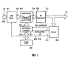
- Figure 3 shows a block diagram of a error decorrelator 25, which comprises a shift block 301, a descrambler 303, a deinterleaver 305, a framer 306, a permutation controller 307 and a DSP 308.
- the shift block 301 receives the received reordered symbol stream 26 on a data connection 300 and puts the FAS sequence on the up most position in the outgoing data connection 302, as will be described in more detail in connection with figure 4 .
- the operation of the descrambler 303 has been described in connection with figure 5 and its implementation will be described in connection with figure 6 .
- a possible implementation of the deinterleaver 305 will be discussed in connection with figure 9 .
- K bit wide data connections 302 and 304 connect the shift block 301 with the descrambler 303 and the descrambler 303 with the deinterleaver 305, respectively.
- Another K bit wide data connection 314 forwards the framed symbol stream 23 output by the deinterleaver 305 to both, the framer 306 and the FEC circuit 22.
- the framer 306 will be discussed in connection with figures 10 to 12 .
- the data connections in figures 2 and 3 may be implemented as buses, which are quite popular in digital circuits.
- the permutation controller 307 may be connected by a unidirectional or bi-directional interface 309 to a DSP 308.
- the DSP 308 just illustrates that the link patterns may be updated by a control interface of the receiver and/or during maintenance. Again, DSP read and write access shall be possible without disturbing the reading of switch control values from the permutation controller 307 for the Benes network.
- Figure 4 illustrates the operation and implementation of the shift block 301, which receives its control signal POS_SHIFT from the framer 306 on shift interface 310 in order to put the FAS sequence on the up most position in the data connection 302.
- a 2K-1 bit wide select connection 401 is formed which constitutes the input of barrel shifter 403. Bits 1 to K-1 of the select connection 401 are directly connected to bits 1 to K-1 of the data connection 300.
- All bits of the data connection 300 including bit 0 are delayed by a delay 402 by a clock cycle T.
- the outputs of the delay of 402 are provided at bits K to 2K-1 of the select connection 401. This means that the symbols present during the previous clock cycle at connection 300 are provided at bits K to 2K-1 of the select connection 401.
- the barrel shifter 403 selects K bits from the select connection 401 and outputs the selected bits at the data connection 302.
- the shift interface 310 is 6 bit wide.
- Table 1 POS_SHIFT bits selected by barrel shifter data connection 302 0 127 to 64 63 to 0 1 126 to 63 63 to 0 ... ... ... 46 81 to 18 63 to 0 47 80 to 17 63 to 0 48 79 to 16 63 to 0 ... ... ... 62 65 to 2 63 to 0 63 64 to 1 63 to 0
- switch (32,x) shall process data bits 63 and 62 of the 64 bit data vector
- switch (31,x) shall process data bits 61 and 60
- switch (1,x) shall process data bits 1 and 0.
- Switch (R,C) is the switch in row R and column C in the (half) Benes network 602 or 601.
- FIG. 7 shows the permutation controller 307 for the descrambler 303, provided that the descrambler 303 comprises a half Benes network 602 as shown in figure 6 .
- the permutation controller 307 comprises a RAM (Random Access Memory) address controller 701, six RAMs 702 to 707 and a multiplexer (MUX) 708.
- the connections 211 and 311 comprise 192 lines, one line for each switch in the half Benes network 602.
- the total RAM has been distributed into six single RAMs 702 to 707, each of which can save 256 words of a length of 32 bits.
- the RAM addresses range from 0 to 255.
- Each of the RAMs 702 to 707 can output one word equivalent to 32 bits at a time which represents one column of the matrix switches.
- the least significant bit (LSB) (bit 0) controls switch (1,x)
- most significant bit (MSB) (bit 31) controls switch (32,x), 1 ⁇ _x ⁇ 6.
- the multiplexer 708 can switch all 192 lines of connection 311 to 0, which makes the half Benes network 602 transparent.
- the multiplexer 708 is controlled by line 709 by the RAM address controller 701.
- the half Benes network 602 is switched transparent e. g. during OOF state to allow FAS search in the subsequent blocks.
- the RAM address controller 701 is connected to the OOF line 312.
- the RAM address controller 701 further receives the frame position information on interface of 313 and outputs a respective RAM address on address interface 710, which is at least 8 bit wide to select a specific word out of 256 words in each RAM. Furthermore, the RAM address controller 701 and to the RAMs 702 to 707 are connected to the DSP 308 by interface 309. This enables a change of the link patterns stored in the RAMs 702 to 707 e. g. during maintenance and disabling of the descrambler for power saving purposes. The advantage of using DSP programmable RAMs is that the link patterns can be optimized for different FEC codes. Interface 309 enables reading from and writing to the RAMs 702 to 707, although in another embodiment interface 309 may only allow writing.
- a PRBS of length 2 16 -1 generated with the polynomial 1 + x + x 3 + x 12 + x 16 has been used.
- This sequence has been generated by a computer and loaded bit wise into the RAMs 702 to 707.
- the first 32 bits of the PRBS are written into RAM 702, address 0, starting with the MSB, the second 32 bits of the PRBS are written into RAM 703, address 0, starting with the MSB and so on until the 161 st to the 192 nd bit, which are the sixth 32 bits, are written to RAM 707, address 0, starting with the MSB again.
- the following 192 bits of the PRBS are written to the address 1 of the RAMs 702 to 707, and so on until address 255 of the RAMs 702 to 707 is set.
- the half Benes network could be controlled by different permutation controllers without RAM. Rather, such different permutation controllers could be based on feed-back shift registers for generating the PRBS.
- the downside of this approach is the high frequency required. In the discussed 5 embodiment 192 bits have to be generated, which are 3 bits per time slot on the optical line, which requires a frequency tree times the line rate. In order to reduce such frequencies, several linear shift registers may be operated in parallel as will be discussed in connection with the second embodiment of a permutation controller shown in figure 8 .
- Another viable approach could be the PRBS calculation by 32 bit or 64 bit microprocessors.
- the permutation controller 207 on the transmitter side and the permutation controller 307 on the receiver side may have different construction, but must produce the same PRBS for synchronization.
- the frame length is FL clock cycles.
- the frame position always starts with 0 when the first occurring bit of a FAS is in the processed K-bit vector.
- the function floor(y) returns the largest integer which is smaller than or equal to y.
- the permutation is changed every 10 clock cycles, 204 words need to be read out of and need to be stored in every RAM. In other embodiments the permutation may be changed more quickly or slowly. If, e. g. the permutation is changed every 8 clock cycles, 255 words need to be comprised in every RAM, in order to avoid a wrap around in a standard frame. The permutation may be changed more slowly, e. g. after 11, 12 ore even 20 clock cycles, in order to avoid wrap around in larger frames than standard frames.
- Fig. 8 shows a second embodiment of a permutation controller.
- This permutation controller does not store all link patterns in a RAM, rather generates the link patterns by 16 parallel PRBS circuits 721, 722, ... and 736.
- the clock frequency of the PRBS circuits 721, 722, ... and 736 is equivalent to the clock frequency of the transmitter reorder block 15 and the error decorrelator 25.
- the clock line 741 is explicitly shown in figure 8 .
- each PRBS circuit has basically the same structure, the same inputs and similar outputs. Therefore only PRBS circuit 721 is shown in more detail.
- the core element of each PRBS circuit is a linear shift register 752 which is 16 bits long. The bits are consecutively numbered from bit 1 at the input to bit 16 at the output. At least two bits are tapped, which are bits 13 and 16 in the embodiment shown in figure 8 . The tapped bits are modulo-two added by one or more XOR gates 753. The result is fed back to the input of the linear shift register 752.
- ROMs 751 are provided which store the initial values, which are loaded in parallel into all linear shift registers 752 upon reset. Therefore, ROMs 751 store different values.
- the maximum length of a PRBS generated by a 16 bit linear shift register is 2 16 -1. Consequently it is desirable to have neighboring PRBS circuits generate parts of the same PRBS sequence which starting positions are equidistant, in this embodiment 2 12 bits apart. By this condition, the values stored in the ROMs 751 may be obtained.
- the clock is divided by frequency divider 743 by a factor 12.
- the frequency divider 743 is reset by interface 313 at the beginning of a new frame. Consequently, the frequency divider 743 outputs a storing signal on line 742 at clock cycles 0, 12, 24 ... after the beginning of a frame, which starts at clock cycle 0.
- bits 5 to 16 of each linear shift register are loaded in parallel into the corresponding buffer 754. While the linear shift register 752 generates the next 12 bits during the following 12 clock cycles, the buffer 754 outputs the previous 12 bits.
- the modify circuit 740 modifies the link patterns output to the multiplexer 708 during the first 48 clock cycles of a frame to ensure that in the 0 th clock cycle bit 0 does not change its position, in the 1 st clock cycle only bit 1 must keep its position, and so on, until in the 47 th clock cycle the last framing bit, bit 47, must keep its position.
- the first link pattern for the first 12 clock cycles may be modified not to change the positions of bits 1 to 12.
- the modification may change from clock cycle to clock cycle or at each second clock cycle in order to generate 12 or 6, respectively, link patterns from the first link pattern.
- a quicker link pattern change may be desirable or a slower link pattern change may be acceptable. Therefore, e. g. only 12 PRBS circuits may be provided for a link pattern change after 16 clock cycles or 24 PRBS circuits may be provided for a link pattern change after 8 clock cycles.
- the length of the buffers 754 must be extended to 16 bits in the first case and may be reduced to 8 bits in the second case.
- Additional circuitry may be provided to use a programmable tapping of the linear shift registers 752 for generating different PRBSs.
- the ROMs 751 may be replaced by RAMs, which may be written by DSP 308.
- the multiplexer 708 operates in the same fashion as in figure 7 .
- the permutation controller 207 for the scrambler 203 differs from the permutation controller 307 only in that the permutation controller 207 does not receive an OOF signal, provided that the scrambler 203 also comprises a half Benes network 602.
- Figure 9 shows the deinterleaver 305, which may be illustrated by a triangle of delays.
- the shift register for bit b comprises K-1-b delays. Each delay delays by one clock cycle T. In other embodiments the delay of each delay could be an integer multiple of one clock cycle, i. e. m*T, m ⁇ 1.
- the shift register for bit b comprises b delays in the interleaver 205. Therefore, the interleaver 205 and the deinterleaver 305 compensate each other by providing a total delay of T(K-1) for each of the K bits. If, in other embodiments, the delay of each delay is an integer multiple of one clock cycle, the total delay is m*T(K-1), m ⁇ 1.
- interleaver 205 and the deinterleaver 305 can be disabled, resulting in 0 delay for each bit.
- FIG 10 shows the framer 306, which comprises a FAS search block 901, a framer supervision block 902, an alarm generation block 903, an error counter 904, a FAS confirm block 905 and a delay 906.
- the framer supervision block 902 comprises an OOF state machine 912 and a frame counter 911.
- the error counter 904 further comprises an LOF state machine 921 and counters 922.
- the deinterleaver 305 and descrambler 303 implement the inverse function of the interleaver 205 and scrambler 203, respectively, the data stream after the deinterleaver can still be disordered because both, the descrambler 303 and the deinterleaver 305 need to be synchronized to the FAS sequence. Therefore the framer 306 must detect the FAS in the data stream. This is explained in more detail in connection with the framing state machines in figures 11 and 12 .
- the FAS search block 901 shall:
- the signal FAS_FOUND shall indicate to the frame supervision block 902 immediately when the FAS_A or FAS_B is detected. Additionally a FRCNT_SET value is determined and provided to the frame supervision block to set the frame counter 911 to the appropriate value to ensure that next occurrence of FAS in the data stream can be supervised.
- Table 2 illustrates an implementation example how the feedback signal POS_SHIFT on the shift interface 310 is generated in dependence from the FAS positions.
- FAS_A when FAS is misaligned (POS_SH)FT not equal to 0) is always detected later to its nominal position X.
- X is the time where FAS is expected on the data bus for FAS confirmation.
- FAS_B detected with POS_SHIFT smaller than 17 is always detected later to its nominal position X.
- FAS_B detected with 5 POS_SHIFT is bigger than 40 is always detected earlier to its nominal position X.
- POS_SHIFT 0 shall be the default value after reset.
- POS_SHIFT shall be set to 0 and hold until a new FAS_A or FAS_B is found and therefore a new POS_SHIFT value was determined.
- the FAS confirm block 905 compares the received data with the correct FAS sequence on positions K-1 to K-48 of the incoming data connection 314.
- the FAS confirm block 905 receives the signal FASPOS signal 935 from the framer supervision block 902 which defines the expected position of the next FAS sequence. It is not sufficient to find the FAS sequence somewhere in the middle of a frame, rather the FAS sequence is only considered valid at the beginning of the following frame.
- the FASPOS signal 935 may be considered an activation signal for the FAS confirm block 905 and may be used for power saving in the FAS confirm block 905, while a FAS sequence is not expected.
- Output 931 to the error counter block are two values FALSE_ONES and FALSE_ZEROS which are the number of false 1 (0 received instead of expected 1) in the FAS, respective number of false 0 (1 received instead of expected 0) together with a pulse FASCNT_UPDATED to indicate that the counters have been updated after each frame.
- Output 932 to the framer supervision block is FAS_OK and to indicate a good FAS and FAS_NOK if FAS is bad.
- FAS_OK In state 1001 two error-free parts FAS_A and FAS_B of a FAS are required for moving to state 1002.
- the received FAS pattern In state 1002 the received FAS pattern may contain a number of acceptable errors 933 FASERR_OK_ALLOW for being considered good (OK).
- FASERR_OK_ALLOW is provided by the register map as control signal.
- the framer supervision block 902 contains the OOF state machine 912 to declare or clear OOF and a frame counter 911 to generate frame synchronous control signals which constitute the frame position information on interface 313.
- the length of the frame FL (distance between two FAS) is defined by a provisioned signal FRM_LENGTH from the register map.
- FRM_LENGTH is the frame length in bits divided by K.
- a typical value for FRM_LENGTH is 2040 (dec).
- FRM_LENGTH may range from 128 to 65535.
- the frame counter 911 shall be reset to a defined value FRCNT_SET when the FAS_FOUND signal is received. This FRCNT_SET value is dependent from the position the FAS was found. In absence of reset and FRCNT_SET signals the frame counter 911 shall run in continuous mode to provide equidistant frame pulses. Via an external resynchronization signal 934 DINT_RESYNCH the frame search can be started manually.
- the error counter block 904 contains the LOF state machine 921 to declare or clear LOF and counters 922 to accumulate errors within the FAS for a defined interval.
- the error counter block 904 receives its information from the FAS confirm block 905 and accumulates the FALSE_ONES and FALSE_ZEROS during an interval of time FASERR_TIME (max 1 second) provided by the register map and considered as static. At the start of each interval the counters start with value zero.
- the error counter block 904 provides the accumulator values FALSE_ONES_ACCU and FALSE_ZEROS_ACCU that are the accumulation results of the last interval to the external register map together with a pulse ACCU_UPDATED whenever a new accumulation value is available which is true at the end of an accumulation interval.
- ACCU_UPDATED is implemented as event bit in the register map and can generate an interrupt.
- the counters shall have a size of 20 bits and saturate at their maximum value when excessive errors are received.
- Figure 11 illustrates the operation of the OOF state machine 912.
- OOF is declared which sets the OOF state machine to state 1001.
- the OOF state machine 912 is also set to state 1001, if in state 1003 an incorrect FAS was detected for FAS_LOOSE consecutive frames.
- the OOF state machine 912 changes from state 1002 to state 1001, if an single incorrect FAS has been detected.
- the OOF state machine goes from state 1001 to state 1002, if a FAS is detected for the first time.
- Figure 12 shows the LOF state machine 921.
- LOF shall be declared and the LOF state machine switch to state 1101 when an OOF condition persists for a minimum of LOFDET_TIME.
- the integrating timer shall not be reset until OOF is inactive for continuously LOFDET_TIME.
- LOF shall be cleared and the LOF state machine 921 be switched to state 1102, when OOF is inactive for continuously LOFCLEAR_TiME.
- the LOFDET_TIME and LOFCLEAR_TIME are provided by register map and considered as static.
- LOFDET_TIME and LOFCLEAR_TIME are specified as number of frames. LOF state is reported to register map.
- the error decorrelator 25 receives a clock and a full synchronous reset signal. This reset shall be used in the combinatorial logic to achieve the required state. It is essential to reset the internal state machines 912 and 921 and the signals to the register map. However it might be a good idea to also reset the complete storage elements.
- the VHDL code needs to be written accordingly to support dynamic clock gating by synthesis.
- the parallelism parameter K is chosen to be equal to Nolnp.
- Perm 5 ⁇ bit NoInp ! - NoInp - 5 !
- a receiver circuit comprising:
- an interleaving or deinterleaving circuit comprising:
- the circuit is preferably characterized by a permutation controller (307) being electrically connected to said network (601; 602), said permutation controller (307) being designed for providing link patterns (501) to said network (601; 602); each link pattern (501) defining the exchanging of said second number of digital symbols provided in parallel on said input (300, 302) of said error decorrelator (25); said permutation controller (307) being designed for changing the link pattern (501) provided to said network (601; 602) from time to time, wherein it is further preferred if the circuit is characterized by a permutation controller (307) comprising a memory (702, 703, 704, 705, 706, 707) for storing a plurality of link patterns (501); said permutation controller (307) further comprising an address controller (701) being electrically connected to said memory (702, 703, 704, 705, 706, 707) for selecting one of said link patterns (501); said memory (702, 703, 704, 705, 706, 707) being connected to said network (601, 602) by an
- circuit is characterized in that said network is a half Benes network (602).
- the circuit further comprising a deinterleaver (305), which comprises a third number of shift registers (800, 860, 861, 862, 863), said third number being equal to said second number minus one; each shift register being operated with the clock which also shifts said parallel streams (26) at said input (300, 302) and output (304, 314); said input (300, 302) comprising said second number of lines being numbered from 0 to said third number minus 1; each line for inputting one symbol during one clock cycle of said clock; said nth line comprising a fourth number of delays, thereby delaying the symbol on the nth line by an integer multiple of said fourth number of clock cycles; said integer being greater than or equal to one; said fourth number being equal to said third number minus n minus 1.
- a deinterleaver (305), which comprises a third number of shift registers (800, 860, 861, 862, 863), said third number being equal to said second number minus one; each shift register being operated with the clock which
- circuit further comprising a framer (306) for detecting a frame alignment signal and for generating frame position information (313) for synchronizing said network (601, 602) to said frame alignment signal.
- a framer circuit comprising:
- circuit described abovefurther comprising:
- a transmitter circuit comprising:
- a receiver circuit comprising:
- a method for a circuit comprising:
- a method for generating a symbol stream for transmission comprising:
- a method for recovering a payload symbol stream (21) from a received reordered symbol stream (26) comprising:
- a method for detecting a sequence of framing bits comprising:
Abstract
Description
- The present invention relates to forward error correction (FEC) e. g. in optical data transmission systems. The invention more specifically relates to separating error bursts, which may result from a Maximum-Likelihood Sequence Estimator (MLSE), into single errors.
- Methods according to the preamble part of
claim 1 are generally known. - An MLSE equalizer is described in
WO 2005/011220 A1 (attorney's ref.: CO4WO), which is incorporated herein by reference. Its purpose is to combat inter-symbol interference (ISI). The applicant recommends MLSE technology for non-coherent optical receivers which use photodiodes for the optical-two-electrical conversion. - The general idea of FEC codes is to calculate a block of m symbols to be transmitted or stored from a block of n message symbols, thereby extending the block of n message symbols by r=m-n redundant symbols. Redundant symbols are also designated parity symbols. Therefore, one may detect and even correct a limited number of wrong symbols within the m-symbol block.
- Several FEC codes are known (cf Wikipedia, English and German version). A BCH (Bose, Chaudhuri, Hocquenghem) code is an error-correcting code that is much studied within coding theory. In technical terms a BCH code is a multilevel, cyclic, error-correcting, variable-length digital code used to correct multiple random error patterns. BCH codes may also be used with multilevel phase-shift keying whenever the number of levels is a prime number or a power of a prime number.
- Reed-Solomon (RS) error correction is an error-correcting code that works by oversampling a polynomial constructed from the data to be transmitted or stored. By sampling the polynomial more often than is necessary, the polynomial is over-determined. As long as "many" of the points are received correctly, the receiver can recover the original polynomial even in the presence of a "few" bad points. Reed-Solomon codes are a sub-class of BCH codes.
- RS codes are specifically useful in combating mixtures of random and burst errors. The downside of RS codes is the extensive arithmetic, which may be an obstacle for real-time and high-speed applications.
- In the compact disc system, error correction and detection is provided by cross-interleaved RS code (CIRC). CIRC consists of an outer RS(24, 28) code, interleaving and an inner RS(28, 32) code. RS(24, 28) means that a block of 24 bytes is encoded to a block of 28 bytes thereby adding 4 redundant bytes. The inner RS(28, 32) code is designed to input an encoded 28-byte block of the outer RS(24, 28) code. During interleaving, a 28 byte input block resulting from the outer code is distributed over 112 output blocks of 28 bytes each. The first byte of the input block lands in the first position of the first output block. The second byte of the input block lands in the second position of the fifth output block and so on until the 28th byte of the input block lands in the 28th position of the 109th output block.
- In this application symbol is mostly used as a synonym for bit. Skilled persons are aware that a symbol is a more general term which may correspond to 2 bits in quadrature phase shift keying or a byte in the context of RS codes.
- For some popular BCH and RS codes integrated circuits have been developed for high-speed optical data transmission. Consequently, the International Telecommunication Union Telecommunication Standardization Sector (ITU-T) has prepared the recommendation G.975.1 titled "Forward error correction for high bit-rate DWDM submarine systems". This Recommendation describes the FEC functions that have higher-correction ability than RS(255,239) code defined in ITU-T Recommendation G.975 for the high bit-rate DWDM (Dense Wavelength Division Multiplexing) submarine cable systems. Nearly all of the codes suggested in Appendix I of recommendation G.975.1 are concatenated codes with an inner and outer code. Some codes comprise interleaving between the inner and outer code as explained in connection with CIRC above.
- ITU-T Recommendation G.709 defines a frame alignment signal (FAS) as 0xF6F6F6282828 (in hexadecimal code), which is a consecutive sequence of 48 bits. A standard frame according to G.709 is 130560 bits long.
- A barrel shifter (cf e. g. Wikipedia) is a digital circuit that can shift a data word by a specified number of bits. It can be implemented as a sequence of multiplexers (MUXs). In this implementation, the output of one MUX is connected to the input of the next MUX in a way that depends on the shift distance. The number of multiplexers required is n*log2(n), for an n bit word. The barrel shifter has a variety of applications, including being a vital component in microprocessors. E. g. for a floating-point add or subtract operation, the mantissae of the numbers must be aligned, which requires shifting the smaller number to the right, increasing its exponent, until it matches the exponent of the larger number.
- In the field of telecommunications, a Clos network (cf e. g. Wikipedia) is a kind of multistage switching network, first formalized by Charles Clos in 1953, which represents a theoretical idealization of practical multi-stage telephone switching systems. Clos networks are required when the physical circuit switching needs exceed the capacity of the largest feasible single crossbar switch. The key advantage of Clos networks is that the number of crosspoints which make up each crossbar switch required can be much fewer than were the entire switching system implemented with one large crossbar switch.
- Clos networks have three stages: the ingress stage, middle stage, and the egress stage. Each stage is made up of a number of crossbar switches, often just called crossbars. Each call entering an ingress crossbar switch can be routed through any of the available middle stage crossbar switches, to the relevant egress crossbar switch.
- Clos networks are defined by three integers n, m, and r. n represents the number of sources which feed into each of r ingress stage crossbar switches. Each ingress stage crossbar switch has m outlets, and there are m centre stage crossbar switches. There is exactly one connection between each ingress stage switch and each middle stage switch. There are r egress stage switches, each with m inputs and n outputs. Each middle stage switch is connected exactly once to each egress stage switch.
- If m ≥ n, the Clos network is rearrangeably nonblocking, meaning that an unused input on an ingress switch can always be connected to an unused output on an egress switch, but for this to take place, existing calls may have to be rearranged by assigning them to different centre stage switches in the Clos network.
- Clos networks may also be generalized to any odd number of stages. By replacing each center stage crossbar switch with a 3-stage Clos network, Clos networks of five stages may be constructed. By applying the same process repeatedly, 7, 9, 11,... stages are possible.
- A rearrangeably nonbocking Clos network of this type with m = n = 2 is generally called a Benes network. The number of inputs and outputs is N = rxn = 2r. Such networks have 2log2N - 1 stages, each containing N/2 2x2 crossbar switches, and use a total of Nlog2N - N/2 2x2 crossbar switches.
- The Benes network may be considered a regular connection structure using a switching element SW which has 2 data inputs I1, 12 and 2 data outputs O1, 02 as base element as shown in
figure 13 . Selection which input drives which output is made by a control signal S. If S=0, I1 is connected to O1 and I2 is connected to 02. If S=1, I1 is connected to O2 and I2 is connected to O1 - The Benes network itself may be considered as a recursive structure and stage s can be derived from (s-1) stage according to
figures 14 . It can easily be seen that the stage s has N = 2 s inputs. An example for a s=2 Benes network is shown infigure 15 . - For parameter s we can derive that the Benes network has following implementation parameters:
- Number of Inputs/Outputs:
NoInp 2 s = N - Number of switches: NoSw = s•2 s - 2 s-1
- Number of stages: NoSt = 2•s - 1
- Number of all permutations: NoPs = s!
- The state of the art further comprises Pseudo Random Binary Sequences, sometimes also referred to as Pseudo Random Bit Sequences (PRBS) (cf e. g. Wikipedia). A binary sequence (BS) is a sequence of N bits,

- A PRBS is random in a sense that the value of an aj element is independent of the values of any of the other elements, similar to real random sequences.
- It is 'pseudo' because it is deterministic and after N elements it starts to repeat itself, unlike real random sequences, such as sequences generated by radioactive decay or by white noise. The PRBS is more general than the n-sequence, which is a special pseudo-random binary sequence of n bits generated as the output of a linear shift register. An n-sequence always has a 1/2 duty cycle and its number of elements N = 2k - 1, k≤n. In real implementations, n-sequences are used as PRBSs due to the efficient generation by linear shift registers.
- The list of the bits positions that influence the input is called the tap sequence, which may be [16,14,13,11]. All bits of the tap sequence are modulo-two added, which may be implemented by 3 XOR gates, each XOR gate xoring two inputs.
- A linear shift register may produce an n-sequence through all possible 2 n - 1 states except the state where all bits are zero, unless it contains all zeros, in which case it will never change. The sequence of numbers generated by a linear shift register can be considered a binary numeral system just as valid as Gray code or the natural binary code.
- The tap sequence of an linear shift register can be represented as a
polynomial modulo 2. This means that the coefficients of the polynomial must be 1's or 0's. This is called the feedback polynomial or characteristic polynomial. For example, if the taps are at the 16th, 14th, 13th and 11th bits (as above), the resulting polynomial is
- The 'one' in the polynomial does not correspond to a tap. The powers of the terms represent the tapped bits, counting from the left, starting with 1.
- For telecommunication purposes, ITU-T O-150 defines several PRBS for bit error rate (BER) and jitter measurements.
- It is the object of this invention to provide an improved receiver, interleaving and deinterleaving circuit and method which make effective use of hardware resources.
- This object is achieved by the subject matter of the independent claims.
- Preferred embodiments of the invention are the subject matter of the dependent claims.
- In the following preferred embodiments of this invention are described referring to the accompanying drawings. In the drawings:
-
Fig. 1 shows a block diagram of an inventive transmission system; -
Fig. 2 shows a block diagram of a transmitter reorder block; -
Fig. 3 shows a block diagram of a error decorrelator; -
Fig. 4 illustrates the operation of a shift block; -
Fig. 5 illustrates an arbitrary link pattern for the inventive scrambler or descrambler; -
Fig. 6 illustrates a Benes network within the inventive scrambler or descrambler; -
Fig. 7 shows a first embodiment of a permutation controller for the inventive scrambler or descrambler; -
Fig. 8 shows a second embodiment of a permutation controller, -
Fig. 9 shows a deinterleaver; -
Fig. 10 shows an inventive framer; -
Fig. 11 shows an OOF state machine; -
Fig. 12 shows a LOF state machine; -
Fig. 13 shows a base element of a Benes network; -
Fig. 14 illustrates the Benes network construction; -
Fig. 15 shows a Benes network for s=2 with four inputs and outputs. -
- BCH:
- Bose, Chaudhuri, Hocquenghem
- BER:
- bit error rate
- BS:
- binary sequence, sometimes also bit sequence
- CIRC:
- cross-interleaved RS code
- DSP:
- digital signal processor
- DWDM:
- dense wavelength division multiplexing
- f:
- line rate
- fK:
- f/K,
- FAS:
- frame alignment signal (ITU G.709)
- FEC:
- forward error correction
- FL:
- frame length
- ISI:
- inter-symbol interference
- ITU:
- International Telecommunication Union
- K:
- bit width, parallelism parameter
- LOF:
- loss of frame
- LSB:
- least significant bit
- MSB:
- most significant bit
- MLSE:
- maximum-likelihood sequence estimator
- MUX:
- multiplexer
- OOF:
- out of frame
- PRBS:
- pseudo random binary sequence, sometimes also pseudo random bit sequence
- RAM:
- random access memory
- ROM:
- read only memory
- RS:
- Reed-Solomon
- s:
- number of stages
- T:
- =1/fK=K/f; delay
- While the present invention is described with reference to the embodiments as illustrated in the following detailed description as well as in the drawings, it should be understood that the following detailed description as well as the drawings are not intended to limit the present invention to the particular illustrative embodiments disclosed, but rather the described illustrative embodiments merely exemplify the various aspects of the present invention, the scope of which is defined by the appended claims.
-
Figure 1 shows a block diagram of an inventive opticaldata transmission system 1. The transmitter comprises a forward error correction (FEC)circuit 12, atransmitter reorder block 15 and anoptical transmitter 19. TheFEC circuit 12 inputs apayload symbol stream 11 to be transmitted and outputs a framedsymbol stream 13 into which redundant symbols have been inserted. Moreover, theFEC circuit 12 inserts framing bits which are used for synchronization purposes on the receiver side. We have assigned this functionality to theFEC circuit 12, which, consequently outputs aframe position information 14 to thetransmitter reorder block 15, which will be explained in more detail in connection withfigure 2 . Thetransmitter reorder block 15 outputs a reorderedsymbol stream 16 to theoptical transmitter 19. The optical transmitter in 19 transforms its electrical input to an optical signal which is transmitted by anoptical fiber 5 to the receiver. - The receiver comprises an
optical receiver 29, anequalizer 27, aerror decorrelator 25 and a forwarderror correction circuit 22. The receiver basically performs the same operations as the transmitter in reversed order to regenerating thepayload symbol stream 21. The reference numbers of corresponding circuit blocks differ by 10. Theoptical receiver 29 converts its optical input into a analog or aquasi-analog output 28. Theequalizer 27 combats inter-symbol interference (ISI) as mentioned above. The output of theequalizer 27 is the designated received reorderedsymbol stream 26, which deviates from the reorderedsymbol stream 16 by a typical BER of 103 to 10-6. The downside of the MLSE technology is that it tends to generate burst errors. Theerror decorrelator 25 separates burst errors such that they appear as isolated single errors in the framedsymbol stream 23. Finally anotherFEC circuit 22 reduces the BER to desired values of 10-9 to 10-16. -
Figure 2 shows a block diagram of atransmitter reorder block 15, which comprises aninterleaver 205, ascrambler 203, apermutation controller 207 and adigital signal processor 208. The framedsymbol stream 13 and the reorderedsymbol stream 16 are conveyed by a data connection which is K bits wide, like most of the data connections used in the embodiments of this invention. Also thedata connection 204 which forwards the output of theinterleaver 205 to thescrambler 203 is K bits wide. Therefore, the clock frequency fK can be by a factor K lower than the line rate f, which is typically in the range of 10 or 40 GHz. A lower clock frequency fK simplifies circuit design and reduces power consumption. K may be 64. - The
interleaver 205 is opposite to deinterleaver 305, which is shown in more detail infigure 9 . Theinterleaver 205 comprises K shift registers indexed from 0 to K-1 forbit 0 to bit K-1, respectively. The shift register forbit 0 has a size of 0, which means that it does not create a delay and may be considered non-existing. The nth shift register for bit n has a size of n, which means that it creates a delay of nT, T being the inverse of the clock rate fK and 0 ≤ n ≤ K-1. In other embodiments the delay of each delay cold be an integer multiple of one clock cycle, i. e. m*T, m≥1. - The operation of the
scrambler 203 may be illustrated byfigure 5 . Thescrambler 203 exchanges the K bits present on thedata connection 204 using alink pattern 501 or, in other words, generates a permutation of such K bits for outputting the reorderedsymbol stream 16. The permutation should be irregular in order to disturb the regularity of theinterleaver 205 for the effective separation of burst errors in the receiver. PRBSs may be used to achieve this irregularity as will be described below. - The
scrambler 203 may be implemented in the same fashion as thedescrambler 303 by aBenes network 601 orhalf Benes network 602. Which permutation or link pattern the Benes orhalf Benes networks permutation controller 207. - The
permutation controller 207 changes the permutation orlink pattern 501 every 10 clock cycles corresponding to 10T, which makes the reordering both on the transmitter and receiver side even less regular. However, for simplifying the detection of the FAS on the receiver side, the permutation sequence is kept constant for K clock cycles equivalent to KT at the beginning of a frame after the FAS. At this point it is only important that the position of the framing bits, which constitute the FAS, is not changed by thescrambler 203, while the link patterns used during the 48 first clock cycles equivalent to 48T may scramble non-framing bits even during the first 48 or first K clock cycles. If framing bits were scrambled, theframer 306 has no chance to find them. This means that the bottom line is that in the 0thclock cycle bit 0 does not change its position, in the 1st clock cycle only bit 1 must keep its position, and so on, until in the 47th clock cycle the last framing bit,bit 47, must keep its position. If a link pattern is changed every 10 clock cycles as indicated above, the first permutation for the first 10 clock cycles transmitsbits 0 to 9 in a one-to-one fashion, the second permutation for the 11 to the 20 clock cycle transmits bits 10 to 19 in a one-to-one fashion and so on. - In another embodiment the link patterns are changed after two clock cycles during the first 64 clock cycles. This embodiment requires less one-to-one connections, namely only 2, in each of the first 32 link patterns, which renders such link patterns less regular, thereby increasing the performance of the error decorrelator 25.For changing the link pattern the
FEC circuit 12 provides theframe position information 14 to thepermutation controller 207. In another embodiment a separate framer before the FEC may be provided, which is not important to this invention.Permutation controllers figure 7 . In particular theconnections half Benes network 602. If thenetwork - It is important that the
permutation controllers descrambler 303 reverses the operation ofscrambler 203. This is also illustrated infigure 5 by the four arrows which represent thedata connection 204, the reorderedsymbol stream 16, and thedata connections framer 306 andfigure 10 . - The
permutation controller 207 may be connected by aninterface 209 to a digital signal processor (DSP) 208. Theinterface 209 may be unidirectional just for writing link patterns from theDSP 208 into thepermutation controller 207 or bi-directional also for reading link patterns from thepermutation controller 207. TheDSP 208 just illustrates that the link patterns may be updated by a control interface of the transmitter and/or during maintenance. In this way different link patterns that are optimized for certain FEC codes may be loaded through the DSP interface. DSP read and write access shall be possible without disturbing the reading of switch control values from thepermutation controller 207 for the Benes network. -
Figure 3 shows a block diagram of aerror decorrelator 25, which comprises ashift block 301, adescrambler 303, adeinterleaver 305, aframer 306, apermutation controller 307 and aDSP 308. Theshift block 301 receives the received reorderedsymbol stream 26 on adata connection 300 and puts the FAS sequence on the up most position in theoutgoing data connection 302, as will be described in more detail in connection withfigure 4 . The operation of thedescrambler 303 has been described in connection withfigure 5 and its implementation will be described in connection withfigure 6 . A possible implementation of thedeinterleaver 305 will be discussed in connection withfigure 9 . K bitwide data connections shift block 301 with thedescrambler 303 and thedescrambler 303 with thedeinterleaver 305, respectively. Another K bitwide data connection 314 forwards the framedsymbol stream 23 output by thedeinterleaver 305 to both, theframer 306 and theFEC circuit 22. Theframer 306 will be discussed in connection withfigures 10 to 12 . The data connections infigures 2 and3 may be implemented as buses, which are quite popular in digital circuits. - E. g. in case of excessive errors, re-establishing a data connection or a reset out of frame (OOF) state is declared by the
framer 306 onOOF line 312 by setting this line to a logical 1. Consequently, thedescrambler 303 is switched to transparent mode by thepermutation controller 307 to allow theframer 306 to carry out FAS search. On the other hand, when the FAS was successfully detected and is found in each frame, theframer 306 provides frame position information on aninterface 313 in a similar fashion asframe position information 14 is provided within the transmitter. Thepermutation controller 307 is discussed in more detail in connection withfigure 7 . Theconnection 311 comprises a line for each switch within thedescrambler 303, i. e. 192 lines for K=64 and ahalf Benes network 601. - Like the
permutation controller 207, thepermutation controller 307 may be connected by a unidirectional orbi-directional interface 309 to aDSP 308. Again, theDSP 308 just illustrates that the link patterns may be updated by a control interface of the receiver and/or during maintenance. Again, DSP read and write access shall be possible without disturbing the reading of switch control values from thepermutation controller 307 for the Benes network. -
Figure 4 illustrates the operation and implementation of theshift block 301, which receives its control signal POS_SHIFT from theframer 306 onshift interface 310 in order to put the FAS sequence on the up most position in thedata connection 302. When in synchronization, then the FAS on thedata connection 302 appears on bits K-1 to K-48 with K-1 to K-24 carry 0b111101101111011 (=0xF6F6F6) and bits K-25 to K-48 carry 0b001010000010100000101 (=0x282828). To this end a 2K-1 bit wideselect connection 401 is formed which constitutes the input ofbarrel shifter 403.Bits 1 to K-1 of theselect connection 401 are directly connected tobits 1 to K-1 of thedata connection 300. All bits of thedata connection 300 includingbit 0 are delayed by adelay 402 by a clock cycle T. The outputs of the delay of 402 are provided at bits K to 2K-1 of theselect connection 401. This means that the symbols present during the previous clock cycle atconnection 300 are provided at bits K to 2K-1 of theselect connection 401. Depending on the POS_SHFT signal thebarrel shifter 403 selects K bits from theselect connection 401 and outputs the selected bits at thedata connection 302. - POS_SHIFT can have values from 0 to K-1, i. e. for K = 64 POS_SHIFT can have values from 0 up to 63. In this case, the
shift interface 310 is 6 bit wide. The following table is an implementation example:Table 1 POS_SHIFT bits selected by barrel shifter data connection 302 0 127 to 64 63 to 0 1 126 to 63 63 to 0 ... ... ... 46 81 to 18 63 to 0 47 80 to 17 63 to 0 48 79 to 16 63 to 0 ... ... ... 62 65 to 2 63 to 0 63 64 to 1 63 to 0 -
Fig. 6 illustrates aBenes network 601 within thescrambler 203 ordescrambler 303 just by showing the 32 switches in each of 11 stages for K=64 input and output bits. With regard to data processing, switch (32,x) shall process data bits 63 and 62 of the 64 bit data vector, switch (31,x) shall process data bits 61 and 60, and so on and finally switch (1,x) shall processdata bits Benes network - Simulation results have shown that the slightly limited number of permutations or link patterns afforded by a
half Benes network 602 do not limit the separating performance of burst errors of theerror decorrelator 25. - For optimum separating performance the "trivial" link pattern in which bit n is linked to bit n and similar link patterns have to be excluded. Only irregular link patterns afford for optimum separating performance. As mentioned above, after the first K clock cycles of a frame, the permutation is changed after every 10 clock cycles. It is desirable that a link pattern is only used once per frame. For a standard G.709 frame with a frame length of 2040 clock cycles at K=64 198 different link patterns are necessary in order to avoid a repetition. Of course, 198 is much smaller than the total number of permutations KI=1.26*1089. Therefore, permutations should be selected which are as much dissimilar as possible.
-
Figure 7 shows thepermutation controller 307 for thedescrambler 303, provided that thedescrambler 303 comprises ahalf Benes network 602 as shown infigure 6 . Thepermutation controller 307 comprises a RAM (Random Access Memory)address controller 701, sixRAMs 702 to 707 and a multiplexer (MUX) 708. As mentioned above, theconnections half Benes network 602. In order to provide that much lines with reasonable input, the total RAM has been distributed into sixsingle RAMs 702 to 707, each of which can save 256 words of a length of 32 bits. The RAM addresses range from 0 to 255. Each of theRAMs 702 to 707 can output one word equivalent to 32 bits at a time which represents one column of the matrix switches. Within one word the least significant bit (LSB) (bit 0) controls switch (1,x) and most significant bit (MSB) (bit 31) controls switch (32,x), 1 ≤_x ≤ 6. - The
multiplexer 708 can switch all 192 lines ofconnection 311 to 0, which makes thehalf Benes network 602 transparent. Themultiplexer 708 is controlled byline 709 by theRAM address controller 701. Thehalf Benes network 602 is switched transparent e. g. during OOF state to allow FAS search in the subsequent blocks. To this end theRAM address controller 701 is connected to theOOF line 312. - The
RAM address controller 701 further receives the frame position information on interface of 313 and outputs a respective RAM address onaddress interface 710, which is at least 8 bit wide to select a specific word out of 256 words in each RAM. Furthermore, theRAM address controller 701 and to theRAMs 702 to 707 are connected to theDSP 308 byinterface 309. This enables a change of the link patterns stored in theRAMs 702 to 707 e. g. during maintenance and disabling of the descrambler for power saving purposes. The advantage of using DSP programmable RAMs is that the link patterns can be optimized for different FEC codes.Interface 309 enables reading from and writing to theRAMs 702 to 707, although in anotherembodiment interface 309 may only allow writing. - In a specific embodiment of this invention, a PRBS of length 216-1 generated with the polynomial

has been used. This sequence has been generated by a computer and loaded bit wise into theRAMs 702 to 707. The first 32 bits of the PRBS are written intoRAM 702,address 0, starting with the MSB, the second 32 bits of the PRBS are written intoRAM 703,address 0, starting with the MSB and so on until the 161st to the 192nd bit, which are the sixth 32 bits, are written to RAM 707,address 0, starting with the MSB again. In a similar fashion the following 192 bits of the PRBS are written to theaddress 1 of theRAMs 702 to 707, and so on until address 255 of theRAMs 702 to 707 is set. - Measurements with other sequences showed that such sequences performed similarly, provided that they had sufficient length without repetition. From this finding one may assume that scheme which governs the writing of the PRBS into the RAMs does not significantly influence the error separating performance.
- From the size of the
RAMs 702 to 707 we obtain a minimum length of 192'256 (=3*214) bit. - In other embodiments the half Benes network could be controlled by different permutation controllers without RAM. Rather, such different permutation controllers could be based on feed-back shift registers for generating the PRBS. The downside of this approach is the high frequency required. In the discussed 5
embodiment 192 bits have to be generated, which are 3 bits per time slot on the optical line, which requires a frequency tree times the line rate. In order to reduce such frequencies, several linear shift registers may be operated in parallel as will be discussed in connection with the second embodiment of a permutation controller shown infigure 8 . Another viable approach could be the PRBS calculation by 32 bit or 64 bit microprocessors. - The
permutation controller 207 on the transmitter side and thepermutation controller 307 on the receiver side may have different construction, but must produce the same PRBS for synchronization. - The frame length is FL clock cycles. The frame position always starts with 0 when the first occurring bit of a FAS is in the processed K-bit vector. One frame ends at frame position FL-1, the next immediately starts at
frame position 0 again. If the frame length is not exactly equal to 64+x*10 clock cycles (x being a positive integer), then the last address being applied will be shorter than 10 clock cycles. - If the frame length exceeds 2614 clock cycles (this is 64 + 255*10) then the RAM addressing shall wrap around and restart with the
first address 0. The RAM address r may be calculated from the clock cycle x after the clock cycle with the FAS, which is assigned 0:

- The function floor(y) returns the largest integer which is smaller than or equal to y. As mentioned above, a standard frame according to G.709 is 130560 bits long, which results in 2040 clock cycles at a parallelism parameter K=64. If the permutation is changed every 10 clock cycles, 204 words need to be read out of and need to be stored in every RAM. In other embodiments the permutation may be changed more quickly or slowly. If, e. g. the permutation is changed every 8 clock cycles, 255 words need to be comprised in every RAM, in order to avoid a wrap around in a standard frame. The permutation may be changed more slowly, e. g. after 11, 12 ore even 20 clock cycles, in order to avoid wrap around in larger frames than standard frames.
- In the embodiment, in which the link pattern is changed after every two clock cycles during the first 64 clock cycles, the following formula apply:


-
Fig. 8 shows a second embodiment of a permutation controller. This permutation controller does not store all link patterns in a RAM, rather generates the link patterns by 16parallel PRBS circuits PRBS circuits transmitter reorder block 15 and theerror decorrelator 25. In n contrast to the other circuit diagrams, theclock line 741 is explicitly shown infigure 8 . - All the PRBS circuits have basically the same structure, the same inputs and similar outputs. Therefore only
PRBS circuit 721 is shown in more detail. The core element of each PRBS circuit is alinear shift register 752 which is 16 bits long. The bits are consecutively numbered frombit 1 at the input to bit 16 at the output. At least two bits are tapped, which arebits figure 8 . The tapped bits are modulo-two added by one ormore XOR gates 753. The result is fed back to the input of thelinear shift register 752. - Since all PRBS circuits generate non-overlapping parts of the same PRBS, the same bits are tapped in each PRBS circuit. For the same reason, different values must be loaded into each linear shift register, when a new frame starts and
interface 313 "resets" allPRBS circuits ROMs 751 are provided which store the initial values, which are loaded in parallel into all linear shift registers 752 upon reset. Therefore,ROMs 751 store different values. The maximum length of a PRBS generated by a 16 bit linear shift register is 216-1. Consequently it is desirable to have neighboring PRBS circuits generate parts of the same PRBS sequence which starting positions are equidistant, in thisembodiment 212 bits apart. By this condition, the values stored in theROMs 751 may be obtained. - The clock is divided by
frequency divider 743 by afactor 12. In addition, thefrequency divider 743 is reset byinterface 313 at the beginning of a new frame. Consequently, thefrequency divider 743 outputs a storing signal online 742 atclock cycles clock cycle 0. When a storing signal is output,bits 5 to 16 of each linear shift register are loaded in parallel into thecorresponding buffer 754. While thelinear shift register 752 generates the next 12 bits during the following 12 clock cycles, thebuffer 754 outputs the previous 12 bits. - The modify
circuit 740 modifies the link patterns output to themultiplexer 708 during the first 48 clock cycles of a frame to ensure that in the 0thclock cycle bit 0 does not change its position, in the 1st clock cycle only bit 1 must keep its position, and so on, until in the 47th clock cycle the last framing bit,bit 47, must keep its position. To this end the first link pattern for the first 12 clock cycles may be modified not to change the positions ofbits 1 to 12. Alternatively the modification may change from clock cycle to clock cycle or at each second clock cycle in order to generate 12 or 6, respectively, link patterns from the first link pattern. The same applies to the second to fourth link patterns for clock cycles 13 to 24, 25 to 36 and 37 to 48, mutatis mutandis. - As mentioned above, a quicker link pattern change may be desirable or a slower link pattern change may be acceptable. Therefore, e. g. only 12 PRBS circuits may be provided for a link pattern change after 16 clock cycles or 24 PRBS circuits may be provided for a link pattern change after 8 clock cycles. The length of the
buffers 754 must be extended to 16 bits in the first case and may be reduced to 8 bits in the second case. - Additional circuitry may be provided to use a programmable tapping of the
linear shift registers 752 for generating different PRBSs. In such embodiments theROMs 751 may be replaced by RAMs, which may be written byDSP 308. - The
multiplexer 708 operates in the same fashion as infigure 7 . - The
permutation controller 207 for thescrambler 203 differs from thepermutation controller 307 only in that thepermutation controller 207 does not receive an OOF signal, provided that thescrambler 203 also comprises ahalf Benes network 602. -
Figure 9 shows thedeinterleaver 305, which may be illustrated by a triangle of delays.Figure 9 is little bit more detailed in that it hints at a shift register for each of the K=64 bits within thedata connections registers bits 0, K-4, K-3, K-2 and K-1, respectively are shown. The shift register for bit b comprises K-1-b delays. Each delay delays by one clock cycle T. In other embodiments the delay of each delay could be an integer multiple of one clock cycle, i. e. m*T, m≥1. - As mentioned above, the shift register for bit b comprises b delays in the
interleaver 205. Therefore, theinterleaver 205 and thedeinterleaver 305 compensate each other by providing a total delay of T(K-1) for each of the K bits. If, in other embodiments, the delay of each delay is an integer multiple of one clock cycle, the total delay is m*T(K-1), m≥1. - For test reasons the
interleaver 205 and thedeinterleaver 305 can be disabled, resulting in 0 delay for each bit. -
Figure 10 shows theframer 306, which comprises aFAS search block 901, aframer supervision block 902, analarm generation block 903, anerror counter 904, aFAS confirm block 905 and a delay 906. Theframer supervision block 902 comprises anOOF state machine 912 and aframe counter 911. Theerror counter 904 further comprises anLOF state machine 921 and counters 922. - Though the
deinterleaver 305 anddescrambler 303 implement the inverse function of theinterleaver 205 andscrambler 203, respectively, the data stream after the deinterleaver can still be disordered because both, thedescrambler 303 and thedeinterleaver 305 need to be synchronized to the FAS sequence. Therefore theframer 306 must detect the FAS in the data stream. This is explained in more detail in connection with the framing state machines infigures 11 and 12 . - The
FAS search block 901 shall: - Detect the FAS sequence by means of K parallel search engines
- Detect on which position the FAS sequence appears within the data bus
- Provide a shift signal by the
frame supervision block 902 to theshift block 301 - Provide a set value to the
frame counter 911 to ensure that next FAS is found on defined position. TheFAS search block 901 provides information to theframer supervision block 902 about the position of the FAS in order to start theframe counter 911 with a defined offset. - Due to timing requirements the FAS search has to be done for K + 47 positions in parallel. This can be done by delaying the data bus by one clock cycle (=T) by delay 906 and combine them with 47 bits of the next clock cycle, which has been explained in more detail in connection with the
shift block 301figure 4 . Theframer 306, however, does not need abarrel shifter 403 shown infigure 4 for the FAS search. - The FAS pattern cannot be searched as a whole 48 bit pattern because a not aligned deinterleaver separates it. Therefore we search for two 24-bit patterns FAS_A=0xF6F6F6 in
FAS_A search block 941 and FAS_B=0x282828 FAS_Bsearch block 942. Search is done as long as the framer supervision block states OOF=1 state and until the first occurrence of FAS_A or FAS_B in the data signal. The signal FAS_FOUND shall indicate to theframe supervision block 902 immediately when the FAS_A or FAS_B is detected. Additionally a FRCNT_SET value is determined and provided to the frame supervision block to set theframe counter 911 to the appropriate value to ensure that next occurrence of FAS in the data stream can be supervised. - The position where the FAS was found within the K + 47 bit search bus is indicated to the shift block by
shift interface 310. - Table 2 illustrates an implementation example how the feedback signal POS_SHIFT on the
shift interface 310 is generated in dependence from the FAS positions.Table 2: Examples of FAS pattern positions for K=64 FAS_A found on position FAS_B found on position shift interface K-17 to K-40 K-41 to K-64 63 ... ... ... K-2 to K-25 K-26 to K-49 48 K-1 to K-24 K-25 to K-48 47 K to K-23 K-24 to K-47 46 K+1 to K-22 K-23 to K-46 45 ... ... ... K+45 to K+22 K+21 to K-2 1 K+46 to K+23 K+22 to K-1 0 - In dependence from POS_SHIFT and the detected FAS_A or FAS_B it is possible to determine the value to which value FRCNT_SET the frame counter needs to be set to ensure that at repetitions of counter value X the next FAS is visible on lines K-48 to K-1 of the connection to block 901, which corresponds to lines K-48 to K-1 of
connection - Generic formulas are provided below, implementation may be differently:

- FAS_A when FAS is misaligned (POS_SH)FT not equal to 0) is always detected later to its nominal position X. X is the time where FAS is expected on the data bus for FAS confirmation. FAS_B detected with POS_SHIFT smaller than 17 is always detected later to its nominal position X. FAS_B detected with 5 POS_SHIFT is bigger than 40 is always detected earlier to its nominal position X.
- If both FAS_A and FAS_B are detected and lead to different POS_SHIFT values, then the result shall be ignored and search continues without providing new FAS_FOUND signal and POS_SHIFT value to the relevant blocks.
- In this example POS_SHIFT = 0 shall be the default value after reset.
- In case when switching from OOF = 0 to OOF = 1 then POS_SHIFT shall be set to 0 and hold until a new FAS_A or FAS_B is found and therefore a new POS_SHIFT value was determined.
- The FAS confirm
block 905 compares the received data with the correct FAS sequence on positions K-1 to K-48 of theincoming data connection 314. In addition, the FAS confirmblock 905 receives the signal FASPOS signal 935 from theframer supervision block 902 which defines the expected position of the next FAS sequence. It is not sufficient to find the FAS sequence somewhere in the middle of a frame, rather the FAS sequence is only considered valid at the beginning of the following frame. TheFASPOS signal 935 may be considered an activation signal for the FAS confirmblock 905 and may be used for power saving in the FAS confirmblock 905, while a FAS sequence is not expected. -
Output 931 to the error counter block are two values FALSE_ONES and FALSE_ZEROS which are the number of false 1 (0 received instead of expected 1) in the FAS, respective number of false 0 (1 received instead of expected 0) together with a pulse FASCNT_UPDATED to indicate that the counters have been updated after each frame. -
Output 932 to the framer supervision block is FAS_OK and to indicate a good FAS and FAS_NOK if FAS is bad. Instate 1001 two error-free parts FAS_A and FAS_B of a FAS are required for moving tostate 1002. Instate 1002 the received FAS pattern may contain a number ofacceptable errors 933 FASERR_OK_ALLOW for being considered good (OK). FASERR_OK_ALLOW is provided by the register map as control signal. - To decide in
state 1003, if the FAS is bad (NOK), the received pattern must exceed a number of acceptable errors FASERR_NOK_EXCEED that is provided by the register map as control signal. - The
framer supervision block 902 contains theOOF state machine 912 to declare or clear OOF and aframe counter 911 to generate frame synchronous control signals which constitute the frame position information oninterface 313. The length of the frame FL (distance between two FAS) is defined by a provisioned signal FRM_LENGTH from the register map. FRM_LENGTH is the frame length in bits divided by K. A typical value for FRM_LENGTH is 2040 (dec). FRM_LENGTH may range from 128 to 65535. Theframe counter 911 shall be reset to a defined value FRCNT_SET when the FAS_FOUND signal is received. This FRCNT_SET value is dependent from the position the FAS was found. In absence of reset and FRCNT_SET signals theframe counter 911 shall run in continuous mode to provide equidistant frame pulses. Via anexternal resynchronization signal 934 DINT_RESYNCH the frame search can be started manually. - The error counter block 904 contains the
LOF state machine 921 to declare or clear LOF and counters 922 to accumulate errors within the FAS for a defined interval. - The
error counter block 904 receives its information from the FAS confirmblock 905 and accumulates the FALSE_ONES and FALSE_ZEROS during an interval of time FASERR_TIME (max 1 second) provided by the register map and considered as static. At the start of each interval the counters start with value zero. Theerror counter block 904 provides the accumulator values FALSE_ONES_ACCU and FALSE_ZEROS_ACCU that are the accumulation results of the last interval to the external register map together with a pulse ACCU_UPDATED whenever a new accumulation value is available which is true at the end of an accumulation interval. ACCU_UPDATED is implemented as event bit in the register map and can generate an interrupt. For further illustration during an accumulation interval the results of the last interval are presented via registers FALSE_ONES_ACCU and FALSE_ZEROS_ACCU. During LOF=1 state the counters shall have an input of zero (counters are on hold), during LOF=0 counters shall normally count the detected errors. - The counters shall have a size of 20 bits and saturate at their maximum value when excessive errors are received.
-
Figure 11 illustrates the operation of theOOF state machine 912. - Following external parameters control the state machine:
- 1. Provided by register map static
- o FAS_CONFIRM: number of consecutive frames for which FAS_OK shall be received
- o FAS_LOOSE: number of consecutive frames for which FAS_NOK shall be received to declare OOF = 1
- o FASERR_OK_ALLOW: number of allowed bit errors in the FAS to still declare FAS_OK
- o FASERR_NOK_EXCEED: number of bit errors which need to be exceeded to declare FAS_NOK
- o D)NT_RESYNCH: resynchronization signal for FAS search (detection of positive edge required)
- 2. Provided by FAS confirm
block 905 andFAS search block 901- o FAS_FOUND: FAS detected for the first time
- o FAS_OK: correct FAS detected
- o FAS_NOK: incorrect FAS detected
- After a reset of the receiver or after a
resynchronization signal 934 is received, OOF is declared which sets the OOF state machine tostate 1001. TheOOF state machine 912 is also set tostate 1001, if instate 1003 an incorrect FAS was detected for FAS_LOOSE consecutive frames. Finally theOOF state machine 912 changes fromstate 1002 tostate 1001, if an single incorrect FAS has been detected. - The OOF state machine goes from
state 1001 tostate 1002, if a FAS is detected for the first time. When entering into thestate 1002 theframe counter 911 is reset to its initial value and frame position information is provided to theshift block 301 by theshift interface 310 and to thepermutation controller 307 byinterface 313. If FAS_CONFIRM consecutive frames with a correct FAS (=FAS_OK) have been received, theOOF state machine 912 goes fromstate 1002 tostate 1003. -
Figure 12 shows theLOF state machine 921. LOF shall be declared and the LOF state machine switch tostate 1101 when an OOF condition persists for a minimum of LOFDET_TIME. The integrating timer shall not be reset until OOF is inactive for continuously LOFDET_TIME. LOF shall be cleared and theLOF state machine 921 be switched tostate 1102, when OOF is inactive for continuously LOFCLEAR_TiME. The LOFDET_TIME and LOFCLEAR_TIME are provided by register map and considered as static. LOFDET_TIME and LOFCLEAR_TIME are specified as number of frames. LOF state is reported to register map. - The
error decorrelator 25 receives a clock and a full synchronous reset signal. This reset shall be used in the combinatorial logic to achieve the required state. It is essential to reset theinternal state machines - In case of descrambler bypass is activated (DINT_BYPASS=1) the
descrambler 303 shall be configured to power safe mode. This shall be done disabling of the clock for thedescrambler 303. The VHDL code needs to be written accordingly to support dynamic clock gating by synthesis. - When bypass is active (DINT_BYPASS=1) the alarms and counter values to the register map shall be set to '0'.
- The
FAS search block 901 is a complex block and power saving is required. In case of OOF=0 the search logic can be disabled until OOF is set to 1. VHDL code needs to be written accordingly to support dynamic clock gating by synthesis under control of the OOF state. - Depending from the size of s following implementation details can be derived for other embodiments:
Table 3: Implementation details for Benes network s Nolnp =K NoSw NoSt Possible Permutations (for 5-bit bursts) Max. Permutations per G.709 frame (standard def.) 8 256 1920 15 1.1*1012 510 7 128 832 13 3.1*1010 1020 6 64 352 11 9.1*108 2040 5 32 144 9 2.4*106 4080 4 16 56 7 5.2*105 8160 3 8 20 5 6720 16320 - The parallelism parameter K is chosen to be equal to Nolnp.
- The number of permutations for a 5-bit burst Perm5bit is calculated as follows:

- It can easily be seen that s = 3 would lead to a repetition of the permutation within one G.709 frame (16320 is bigger than 6720). All other combinations of the table 3 can satisfy the request that a permutation shall be unique within one frame.
- Turning now to the distribution of errors for delay deinterleaver, we may consider an error burst of length R with bits X0, X1, ..., XR-1 in the incoming data stream. We want to understand how bits are distributed after passing the
synchronized deinterleaver 305. The minimum distance between Xr and Xr+1 after delay deinterleaving is given by K-1. - The structure of the
deinterleaver 305 separates an error burst of R <= K always into individual bits. Error bursts of R > K will result in neighboring bits Xr and Xr+K+1 after deinterleaving. - For example if R = K+7 then we would find 7 neighbored pairs of bits as are XK-7 and X6, XK+6 and X5 and so on to XK+1 and X0.
- When the
Benes network 601 is set to transparent mode, with the given sets of parameters we achieveTable 4: Error distribution dependent from mode K Max burst length to avoid double errors (:= MBL) Min distance between 2 errors if R <= MBL Distance between 2 neighbor errors 64 64 65 65 - Further modifications and variations of the present invention will be apparent to those skilled in the art in view of this description. Accordingly, this description is to be construed as illustrative only and is for the purpose of teaching those skilled in the art the general manner of carrying out the present invention. It is to be understood that the forms of the invention shown and described herein are to be taken as the presently preferred embodiments.
- In summary, according to an aspect it is provided a receiver circuit comprising:
- an equalizer (27) comprising an input and an output; said input of said equalizer (27) for receiving a symbol stream (28) and said output of said equalizer (27) for outputting a symbol stream (26);
- characterized by
- an error decorrelator (25) comprising an input and output; said input of said error decorrelator (25) being connected to said output of said equalizer (27);
- said error decorrelator (25) being configured for changing (501; 601, 602) the position of at least half of a first number of symbols within said symbols stream (26) received at said input of said error decorrelator (25) thereby generating a symbols stream (23) of exchanged symbols at said output of said error decorrelator (25),
- wherein the circuit is preferably characterized in that said equalizer being a maximum-likelihood sequence estimator (27), and/or
- wherein the circuit is preferably characterized in that
- said input (300, 302) of said error decorrelator (25) being configured for receiving a parallel stream of digital symbols, said parallel stream (302) being a second number of symbols wide;
- said error decorrelator (25) further comprising a network (601; 602) for exchanging at least half of said second number of digital symbols provided in parallel on said input (300, 302) of said error decorrelator (25); and
- said output (304, 314) of said error decorrelator (25) for outputting said second number of exchanged digital symbols.
- In another aspect it is provided an interleaving or deinterleaving circuit comprising:
- an input (13, 204; 300, 302) for receiving a parallel stream of a second number of digital symbols, said parallel stream (302) being a second number of symbols wide;
- a network (601; 602) for exchanging at least half of said second number of digital symbols provided in parallel on said input (13, 204; 300, 302); and
- an output (16; 304, 314) for outputting said second number of exchanged digital symbols.
- In the above aspects, the circuit is preferably characterized by a permutation controller (307) being electrically connected to said network (601; 602), said permutation controller (307) being designed for providing link patterns (501) to said network (601; 602); each link pattern (501) defining the exchanging of said second number of digital symbols provided in parallel on said input (300, 302) of said error decorrelator (25); said permutation controller (307) being designed for changing the link pattern (501) provided to said network (601; 602) from time to time,
wherein it is further preferred if the circuit is characterized by a permutation controller (307) comprising a memory (702, 703, 704, 705, 706, 707) for storing a plurality of link patterns (501); said permutation controller (307) further comprising an address controller (701) being electrically connected to said memory (702, 703, 704, 705, 706, 707) for selecting one of said link patterns (501); said memory (702, 703, 704, 705, 706, 707) being connected to said network (601, 602) by an electrical connection (311) for outputting said selected link pattern to said network (602), or
wherein the circuit is preferably characterized by a permutation controller (307) comprising a linear shift register (752); at least two stages of said shift register are tapped and connected to an XOR circuit (753) for modulo-two adding the tapped bits and calculating an input for said linear shift register. - It is further preferred that the circuit is characterized in that said network is a half Benes network (602).
- It is further preferred that the circuit further comprising a deinterleaver (305), which comprises a third number of shift registers (800, 860, 861, 862, 863), said third number being equal to said second number minus one; each shift register being operated with the clock which also shifts said parallel streams (26) at said input (300, 302) and output (304, 314); said input (300, 302) comprising said second number of lines being numbered from 0 to said third number minus 1; each line for inputting one symbol during one clock cycle of said clock; said nth line comprising a fourth number of delays, thereby delaying the symbol on the nth line by an integer multiple of said fourth number of clock cycles; said integer being greater than or equal to one; said fourth number being equal to said third number minus
n minus 1. - It is further preferred that the circuit further comprising a framer (306) for detecting a frame alignment signal and for generating frame position information (313) for synchronizing said network (601, 602) to said frame alignment signal.
- According to another aspect it is provided a framer circuit comprising:
- a FAS search block (901) characterized by being configured for performing two searches, a first search (941) for a first part of a sequence of framing bits and a second search (942) for a second part of said sequence of framing bits, said first and second parts together forming said sequence of framing bits.
- It if further preferred that the above described circuit further comprising a framer (306) comprising:
- a FAS confirm block (905) whose input being electrically connected (314) to said output (304) for confirming as to whether a frame alignment signal is found at an expected position;
- a frame counter (911) for counting the clock cycles since the recently detected frame alignment signal, thereby generating frame position information (313);
- said frame counter (911) being electrically connected (932) to said FAS confirm block (905) and said permutation controller (307) which provides one of said link patterns (501) based on said frame position information (313); and
- a FAS search block (901) as defined above.
- Preferably, the circuit described abovefurther comprising:
- a shift block (301) for receiving a parallel, reordered stream (26, 300) of a second number of digital symbols, said shift block comprises a delay (402) and
- a shifter (403),
- said delay (402) for receiving said parallel, reordered stream (26, 300) for outputting the previous symbols of said parallel, reordered stream (26, 300); and
- said shifter (403) for receiving the present symbols of said parallel, reordered stream (26, 300) and said previous symbols of said parallel, reordered stream (26, 300); an output of said shifter being electrically connected to said input (302) for outputting said second number of symbols in parallel, which comprise a frame alignment signal on the up most position, if said frame alignment signal is comprised in said second number of output symbols; and
- a frame supervision block (902) being electrically connected (310) to said shifter (403) for providing shift information for putting said frame alignment signal on the up most position.
- According to another aspect, it is provided a transmitter circuit comprising:
- an FEC circuit (12) having an input for inputting a payload symbol stream (11) comprising payload symbols; said FEC circuit (12) having an output; said FEC circuit (12) being designed for calculating coded symbols by applying an FEC code to said payload symbols; and
- a reorder block (15) having an input and an output; said reorder block (15) being designed for changing the positions of the symbols inputted by said input thereby obtaining a reordered symbol stream (16); said reorder block (15) being further designed for outputting said reordered symbol stream (16) at said output of said reorder block (15);
- characterized in that
- said FEC circuit (12) is further designed for outputting a framed symbol stream comprising framing symbols and coded symbols; and
- the input of said reorder block (15) is connected to said output of said FEC circuit (12),
- wherein said reorder block (15) preferably further comprising a circuit described above.
- According to another aspect, it is provided a receiver circuit comprising:
- an error decorrelator (25) having an input and an output; said input for inputting a received reordered symbol stream (26); said error decorrelator (25) being designed for changing the positions of the symbols within said received reordered symbol stream (26); and
- an FEC circuit (22) having an input for inputting a symbol stream (23) comprising coded symbols; said FEC circuit (22) having an output for outputting a payload symbol stream; said FEC circuit (22) being designed for recovering said payload symbols from coded symbols;
- characterized in that
- said error decorrelator (25) outputs a framed symbol stream (23) comprising framing symbols and said coded symbols; and
- said input of said FEC circuit (22) being electrically connected to said output of said error decorrelator (25),
- wherein the receiver preferably further comprising one ore more parts of the circuits described above.
- According to another aspect it is provided a method for a circuit comprising:
- equalizing (27) a stream of symbols (28) thereby obtaining an equalized symbol stream (26);
- characterized by
- changing (501; 601, 602) the position of at least half of a first number of symbols within said equalized symbols stream (26) thereby generating a symbols stream (23) of exchanged symbols.
- According to another aspect, it is provided a method comprising:
- selecting a second number of symbols (204; 302) within a stream of digital data (13; 28) thereby obtaining selected symbols;
- characterized by
- exchanging (501; 601, 602) the position of at least half of said second number of symbols of said selected symbols with the position of other symbols from said selected symbols; symbols of said selected symbols which are not exchanged remain at their position,
- grouping symbols of a stream of digital data (26) into blocks of symbols (304),
- each block of symbols comprises a third number of symbols; and
- delaying (800, 860, 861, 862, 863) the nth symbol within each block by a fourth number of blocks, said fourth number being equal to an integer multiple of a fifth number, said integer being greater than or equal to one, said fifth number being equal to said third number minus n minus 1, n ranging from 0 to said third number minus one, and/or
- repeating said selecting and said exchanging (601, 602) a sixth number of times by using a fixed link pattern (501) in the exchanging step;
- switching (307) to a different link pattern (501), after said selecting and said exchanging (501; 601, 602) have been performed another sixth number of times.
- According to another aspect, it is provided a method for generating a symbol stream for transmission comprising:
- obtaining (12) a framed symbol stream comprising framing symbols and coded symbols; said obtaining comprising calculating said coded symbols by applying an FEC code to payload symbols of an input payload symbol stream; and
- changing (15) the positions of symbols thereby obtaining a reordered symbol stream (16);
- characterized in that
- the positions of symbols in said framed symbol stream (13) are changed for obtaining said reordered symbol stream (16).
- According to another aspect, it is provided a method for recovering a payload symbol stream (21) from a received reordered symbol stream (26) comprising:
- changing the positions of the symbols within said received reordered symbol stream (26);
- recovering (22) payload symbols (21) from coded symbols;
- characterized in that
- the result of said changing is a framed symbol stream (23) comprising framing symbols and said coded symbols.
- According to another aspect, it is provided a method for detecting a sequence of framing bits comprising:
- performing a first search (941) for a first part of said sequence of framing bits characterized by
- a second search (942) for a second part of said sequence of framing bits, said first and second parts together forming said sequence of framing bits.
-
- 1
- optical data transmission system
- 5
- optical fiber
- 11
- payload symbol stream
- 12
- forward error correction (FEC) circuit
- 13
- framed symbol stream
- 14
- frame position information
- 15
- transmitter reorder block
- 16
- symbol stream
- 19
- optical transmitter
- 21
- payload symbol stream
- 22
- forward error correction circuit
- 23
- framed symbol stream
- 25
- error decorrelator
- 26
- received reordered symbol stream
- 27
- equalizer
- 28
- quasi-analog output
- 29
- optical receiver
- 203
- scrambler
- 204
- data connection
- 205
- interleaver
- 207
- permutation controller
- 208
- digital signal processor
- 209
- interface
- 211
- connection
- 300, 302,
- 304, 314 data connection
- 301
- shift block
- 303
- descrambler
- 305
- deinterleaver
- 306
- framer
- 307
- permutation controller
- 308
- DSP
- 309
- bi-directional interface
- 310
- shift interface
- 311
- connection
- 312
- OOF line
- 313
- interface
- 401
- select connection
- 402
- delay
- 403
- barrel shifter
- 501
- link pattern
- 601
- Benes network
- 602
- Benes network
- 302, 304
- data connections
- 701
- address controller
- 702, 703,
- 704, 705, 706, 707 RAM
- 708
- multiplexer
- 710
- address interface
- 721
- PRBS circuit
- 740
- modify circuit
- 741
- clock line
- 742
- line
- 743
- frequency divider
- 751
- ROM
- 752
- linear shift register
- 753
- XOR gate
- 754
- buffer
- 721,
- 722, ... 736 PRBS circuit
- 800, 860,
- 861, 862, 863 shift register
- 901
- FAS search block
- 902
- framer supervision block
- 903
- alarm generation block
- 904
- error counter
- 905
- FAS confirm block
- 906
- delay
- 911
- frame counter
- 912
- OOF state machine
- 921
- LOF state machine
- 922
- counters
- 931, 932
- output
- 933
- allowed errors
- 934
- resynchronization signal
- 935
- FASPOS signal
- 941
- FAS_A search block
- 942
- FAS_B search block
- 1001,
- 1002, 1003, 1101, 1102 states
Claims (11)
- A framer circuit comprising:a FAS search block (901) characterized by being configured for performing two searches, a first search (941) for a first part of a sequence of framing bits and a second search (942) for a second part of said sequence of framing bits, said first and second parts together forming said sequence of framing bits.
- The framer circuit according to claim 1, further comprising:a FAS confirm block (905) configured to confirm as to whether a frame alignment signal is found at an expected position; anda frame counter (911) configured to count the clock cycles since the recently detected frame alignment signal, thereby generating frame position information (313), said frame counter (911) being electrically connected (932) to said FAS confirm block (905).
- The framer circuit according to claim 1 or 2, further comprising:a framer supervision block (902) configured to provide a shift signal on a shift interface (310), wherein the FAS search block (901) is configured to provide information to the framer supervision block (902) about the position of the FAS.
- The circuit of claim 1, further comprising:a shift block (301) for receiving a parallel, reordered stream (26, 300) of a second number of digital symbols, said shift block comprises a delay (402) and a shifter (403),
said delay (402) for receiving said parallel, reordered stream (26, 300) for outputting the previous symbols of said parallel, reordered stream (26, 300); and said shifter (403) for receiving the present symbols of said parallel, reordered stream (26, 300) and said previous symbols of said parallel, reordered stream (26, 300); an output of said shifter being electrically connected to said input (302) for outputting said second number of symbols in parallel, which comprise a frame alignment signal on the up most position, if said frame alignment signal is comprised in said second number of output symbols; anda framer supervision block (902) being electrically connected (310) to said shifter (403) for providing shift information for putting said frame alignment signal on the up most position. - The circuit according to claim 3 or 4, wherein the framer supervision block (902) comprises a frame counter (911) configured to generate frame synchronous control signals which constitute frame position information on an interface (313) of the framer circuit, and wherein the FAS search block (901) is configured to provide information to the framer supervision block (902) about the position of the FAS in order to start the frame counter (911) with a defined offset.
- The circuit according to any one of claims 3 to 5, wherein the framer supervision block (902) comprises an OOF state machine (912) configured to declare or clear an OOF state on an OOF line (312) of the framer circuit.
- A circuit comprising:a permutation controller (307) configured to provide link patterns (501), each link pattern defining (501) defining an exchanging of a second number of digital symbols, wherein said permutation controller (307) is configured to changing the link pattern (501) from time to time; anda framer circuit according to claim 2, wherein said frame counter (911) is electrically connected to said permutation controller (307) which provides one of said link patterns (501) based on said frame position information (313).
- A method for a circuit comprising:equalizing (27) a stream of symbols (28) thereby obtaining an equalized symbol stream (26);characterized bychanging (501; 601, 602) the position of at least half of a first number of symbols within said equalized symbols stream (26) thereby generating a symbols stream (23) of exchanged symbols.
- A method for generating a symbol stream for transmission comprising:obtaining (12) a framed symbol stream comprising framing symbols and coded symbols; said obtaining comprising calculating said coded symbols by applying an FEC code to payload symbols of an input payload symbol stream; andchanging (15) the positions of symbols thereby obtaining a reordered symbol stream (16);characterized in thatthe positions of symbols in said framed symbol stream (13) are changed for obtaining said reordered symbol stream (16).
- A method for recovering a payload symbol stream (21) from a received reordered symbol stream (26) comprising:changing the positions of the symbols within said received reordered symbol stream (26);recovering (22) payload symbols (21) from coded symbols;characterized in thatthe result of said changing is a framed symbol stream (23) comprising framing symbols and said coded symbols.
- A method for detecting a sequence of framing bits comprising:performing a first search (941) for a first part of said sequence of framing bits characterized bya second search (942) for a second part of said sequence of framing bits, said first and second parts together forming said sequence of framing bits.
Priority Applications (1)
| Application Number | Priority Date | Filing Date | Title |
|---|---|---|---|
| EP11008793.9A EP2437398B1 (en) | 2007-10-15 | 2008-10-10 | Receiver, interleaving and deinterleaving circuit and method |
Applications Claiming Priority (3)
| Application Number | Priority Date | Filing Date | Title |
|---|---|---|---|
| EP07118489A EP2051387A1 (en) | 2007-10-15 | 2007-10-15 | Receiver, interleaving and deinterleaving circuit and method |
| EP08838908.5A EP2097983B1 (en) | 2007-10-15 | 2008-10-10 | Receiver, interleaving and deinterleaving circuit and method |
| EP11008793.9A EP2437398B1 (en) | 2007-10-15 | 2008-10-10 | Receiver, interleaving and deinterleaving circuit and method |
Related Parent Applications (3)
| Application Number | Title | Priority Date | Filing Date |
|---|---|---|---|
| EP08838908.5A Division EP2097983B1 (en) | 2007-10-15 | 2008-10-10 | Receiver, interleaving and deinterleaving circuit and method |
| EP08838908.5A Division-Into EP2097983B1 (en) | 2007-10-15 | 2008-10-10 | Receiver, interleaving and deinterleaving circuit and method |
| EP08838908.5 Division | 2008-10-10 |
Publications (3)
| Publication Number | Publication Date |
|---|---|
| EP2437398A2 true EP2437398A2 (en) | 2012-04-04 |
| EP2437398A3 EP2437398A3 (en) | 2012-05-09 |
| EP2437398B1 EP2437398B1 (en) | 2015-03-18 |
Family
ID=39326955
Family Applications (3)
| Application Number | Title | Priority Date | Filing Date |
|---|---|---|---|
| EP07118489A Withdrawn EP2051387A1 (en) | 2007-10-15 | 2007-10-15 | Receiver, interleaving and deinterleaving circuit and method |
| EP11008793.9A Active EP2437398B1 (en) | 2007-10-15 | 2008-10-10 | Receiver, interleaving and deinterleaving circuit and method |
| EP08838908.5A Active EP2097983B1 (en) | 2007-10-15 | 2008-10-10 | Receiver, interleaving and deinterleaving circuit and method |
Family Applications Before (1)
| Application Number | Title | Priority Date | Filing Date |
|---|---|---|---|
| EP07118489A Withdrawn EP2051387A1 (en) | 2007-10-15 | 2007-10-15 | Receiver, interleaving and deinterleaving circuit and method |
Family Applications After (1)
| Application Number | Title | Priority Date | Filing Date |
|---|---|---|---|
| EP08838908.5A Active EP2097983B1 (en) | 2007-10-15 | 2008-10-10 | Receiver, interleaving and deinterleaving circuit and method |
Country Status (4)
| Country | Link |
|---|---|
| US (2) | US8555132B2 (en) |
| EP (3) | EP2051387A1 (en) |
| JP (1) | JP5464752B2 (en) |
| WO (1) | WO2009050121A1 (en) |
Families Citing this family (18)
| Publication number | Priority date | Publication date | Assignee | Title |
|---|---|---|---|---|
| EP2051387A1 (en) | 2007-10-15 | 2009-04-22 | CoreOptics, Inc., c/o The Corporation Trust Center | Receiver, interleaving and deinterleaving circuit and method |
| US20120174187A1 (en) * | 2009-07-09 | 2012-07-05 | Georgia Tech Research Corporation | Systems and methods for providing physical layer security |
| US8302043B2 (en) * | 2009-09-17 | 2012-10-30 | International Business Machines Corporation | Verification of logic circuit designs using dynamic clock gating |
| US8718491B2 (en) | 2009-10-29 | 2014-05-06 | Ciena Corporation | Soft decoding of data in a coherent optical receiver |
| US8565271B2 (en) * | 2011-04-01 | 2013-10-22 | Opnext Subsystems, Inc. | Multiplexer lane alignment for high-speed data systems |
| US8601340B2 (en) | 2011-07-25 | 2013-12-03 | Cortina Systems, Inc. | Time varying data permutation apparatus and methods |
| US9575834B2 (en) * | 2014-05-16 | 2017-02-21 | International Business Machines Corporation | Detecting single event upsets and stuck-at faults in RAM-based data path controllers |
| US9560427B2 (en) * | 2014-05-28 | 2017-01-31 | Huawei Technologies Co., Ltd. | Scalable silicon photonic switching architectures for optical networks |
| US11178072B2 (en) * | 2015-06-10 | 2021-11-16 | Mobileye Vision Technologies Ltd. | Image processor and methods for processing an image |
| US10469199B2 (en) * | 2016-09-09 | 2019-11-05 | Viavi Solutions Inc. | Forward error correction with optical and electrical transponder |
| US9998146B2 (en) * | 2016-10-28 | 2018-06-12 | Inphi Corporation | Forward error correction (FEC) emulator |
| WO2018187902A1 (en) | 2017-04-10 | 2018-10-18 | Qualcomm Incorporated | An efficient interleaver design for polar codes |
| WO2019116106A2 (en) * | 2017-12-14 | 2019-06-20 | Mobileye Vision Technologies Ltd. | Image processor and methods for processing an image |
| US10216567B1 (en) * | 2018-08-22 | 2019-02-26 | Avago Technologies International Sales Pte. Limited | Direct parity encoder |
| RU2718579C1 (en) * | 2019-05-20 | 2020-04-08 | Антон Юрьевич Баринов | Fast pseudorandom interleaver |
| FR3103070B1 (en) * | 2019-11-13 | 2024-03-22 | Univ Grenoble Alpes | Method for synchronizing a communication system based on data retransmission |
| US11748195B2 (en) * | 2022-01-05 | 2023-09-05 | International Business Machines Corporation | Detect multifold disturbance and minimize read-disturb errors in NAND flash |
| CN114430305B (en) * | 2022-03-02 | 2023-06-09 | 烽火通信科技股份有限公司 | Frame fixing method and system for fine-grained frames |
Citations (1)
| Publication number | Priority date | Publication date | Assignee | Title |
|---|---|---|---|---|
| WO2005011220A1 (en) | 2003-07-02 | 2005-02-03 | Coreoptics Inc. | Channel estimation and sequence estimation for the reception of optical signal |
Family Cites Families (39)
| Publication number | Priority date | Publication date | Assignee | Title |
|---|---|---|---|---|
| GB2103053A (en) | 1981-06-02 | 1983-02-09 | British Broadcasting Corp | Improvements relating to transmission of data in blocks |
| US4559625A (en) * | 1983-07-28 | 1985-12-17 | Cyclotomics, Inc. | Interleavers for digital communications |
| US4547887A (en) * | 1983-11-30 | 1985-10-15 | The United States Of America As Represented By The Secretary Of The Army | Pseudo-random convolutional interleaving |
| JPH063589B2 (en) * | 1987-10-29 | 1994-01-12 | インターナシヨナル・ビジネス・マシーンズ・コーポレーシヨン | Address replacement device |
| JPH0326337A (en) | 1989-06-21 | 1991-02-04 | Tosoh Corp | Isomerization catalyst |
| JPH03262337A (en) * | 1990-03-09 | 1991-11-22 | Otc Ltd | Adaptive equalizer and digital data interpolation |
| JPH04220030A (en) * | 1990-12-19 | 1992-08-11 | Alpine Electron Inc | Data communication system |
| JP2755067B2 (en) * | 1992-09-25 | 1998-05-20 | 日本電気株式会社 | Frame synchronization circuit |
| US5729559A (en) * | 1995-03-27 | 1998-03-17 | Motorola, Inc. | Method and apparatus for correcting errors using multiple estimates |
| JPH08287617A (en) | 1995-04-14 | 1996-11-01 | Toshiba Corp | Data transmission method, data transmitting/recording device, data reproducing device and recording medium |
| JPH08331553A (en) * | 1995-05-31 | 1996-12-13 | Alpine Electron Inc | Voice signal processing unit for bs tuner |
| US5734676A (en) * | 1996-05-24 | 1998-03-31 | International Business Machines Corporation | Apparatus, method and article of manufacture for carrier frequency compensation in a FM radio receiver |
| US6018523A (en) * | 1997-10-22 | 2000-01-25 | Lucent Technologies, Inc. | Switching networks having improved layouts |
| JP4533472B2 (en) * | 1998-03-19 | 2010-09-01 | 富士通株式会社 | Optical amplification device, optical output control method using optical amplification device, and optical transmission device |
| JP2000165325A (en) * | 1998-11-30 | 2000-06-16 | Nec Corp | Transmission output control system for optical communication unit |
| US6366624B1 (en) * | 1998-11-30 | 2002-04-02 | Ericsson Inc. | Systems and methods for receiving a modulated signal containing encoded and unencoded bits using multi-pass demodulation |
| US6154452A (en) | 1999-05-26 | 2000-11-28 | Xm Satellite Radio Inc. | Method and apparatus for continuous cross-channel interleaving |
| JP4207329B2 (en) * | 1999-09-20 | 2009-01-14 | 富士通株式会社 | Frame synchronization circuit |
| JP3770767B2 (en) * | 2000-02-17 | 2006-04-26 | 株式会社日立製作所 | Transponder, wavelength division multiplexing transmission apparatus, wavelength division multiplexing transmission system, and information communication apparatus |
| US6971057B1 (en) * | 2000-02-25 | 2005-11-29 | Globespanvirata, Inc. | System and method for efficient convolutional interleaving/de-interleaving |
| US6606718B1 (en) * | 2000-05-11 | 2003-08-12 | Agere Systems Inc. | Product code with interleaving to enhance error detection and correction |
| JP2001326671A (en) * | 2000-05-17 | 2001-11-22 | Nec Corp | Optical communication unit and inter-vehicle lan system using the same |
| JP3668673B2 (en) * | 2000-06-09 | 2005-07-06 | 株式会社日立コミュニケーションテクノロジー | Error correction code configuration method, decoding method, transmission apparatus, network |
| AU2001269086A1 (en) * | 2000-07-04 | 2002-01-14 | Koninklijke Philips Electronics N.V. | Substitution-box for symmetric-key ciphers |
| US6738392B1 (en) * | 2000-09-27 | 2004-05-18 | Cisco Technology, Inc. | Method and apparatus of framing high-speed signals |
| US6873613B1 (en) * | 2000-10-16 | 2005-03-29 | Ericsson Inc. | Methods for wirelessly communicating time division multiple access (TDMA) data using adaptive multiplexing and coding |
| JP2002150698A (en) * | 2000-11-06 | 2002-05-24 | Pioneer Electronic Corp | Method and device for recording information and method and device for reproducing information |
| DE60127944T2 (en) * | 2001-06-08 | 2007-09-06 | Sony Deutschland Gmbh | MULTI-CARRIER SYSTEM WITH ADAPTIVE BITWEISER NESTING |
| DE60112445T2 (en) * | 2001-10-10 | 2006-04-06 | Matsushita Electric Industrial Co., Ltd., Kadoma | Modification of an interleaver pattern |
| US20030072328A1 (en) * | 2001-10-15 | 2003-04-17 | Echartea Jesus Palomino | Framing data in a control circuit |
| US7593411B2 (en) * | 2002-02-21 | 2009-09-22 | Pmc-Sierra, Inc. | Bus interface for transfer of multiple SONET/SDH rates over a serial backplane |
| JP2005110228A (en) | 2003-09-10 | 2005-04-21 | Matsushita Electric Ind Co Ltd | Secure communication method, transmitting device, and receiving device |
| JP4379251B2 (en) | 2004-08-02 | 2009-12-09 | トヨタ自動車株式会社 | Control device and control method for internal combustion engine |
| KR100912156B1 (en) * | 2005-02-03 | 2009-08-14 | 파나소닉 주식회사 | Parallel interleaver, parallel deinterleaver, and interleave method |
| TWI290426B (en) * | 2005-02-03 | 2007-11-21 | Sanyo Electric Co | Encryption processing circuit |
| US7657818B2 (en) * | 2005-06-22 | 2010-02-02 | Adaptive Spectrum And Signal Alignment, Inc. | Dynamic minimum-memory interleaving |
| KR100797176B1 (en) * | 2005-10-21 | 2008-01-23 | 삼성전자주식회사 | Digital broadcasting system and method thereof |
| JP4317860B2 (en) * | 2006-08-30 | 2009-08-19 | 株式会社日立コミュニケーションテクノロジー | Optical concentrator and optical subscriber unit |
| EP2051387A1 (en) | 2007-10-15 | 2009-04-22 | CoreOptics, Inc., c/o The Corporation Trust Center | Receiver, interleaving and deinterleaving circuit and method |
-
2007
- 2007-10-15 EP EP07118489A patent/EP2051387A1/en not_active Withdrawn
- 2007-10-25 US US11/924,397 patent/US8555132B2/en active Active
-
2008
- 2008-10-10 EP EP11008793.9A patent/EP2437398B1/en active Active
- 2008-10-10 WO PCT/EP2008/063631 patent/WO2009050121A1/en active Application Filing
- 2008-10-10 EP EP08838908.5A patent/EP2097983B1/en active Active
- 2008-10-10 JP JP2010528413A patent/JP5464752B2/en not_active Expired - Fee Related
-
2013
- 2013-08-02 US US13/957,639 patent/US8874988B2/en active Active
Patent Citations (1)
| Publication number | Priority date | Publication date | Assignee | Title |
|---|---|---|---|---|
| WO2005011220A1 (en) | 2003-07-02 | 2005-02-03 | Coreoptics Inc. | Channel estimation and sequence estimation for the reception of optical signal |
Also Published As
| Publication number | Publication date |
|---|---|
| US20130318417A1 (en) | 2013-11-28 |
| EP2051387A1 (en) | 2009-04-22 |
| EP2437398B1 (en) | 2015-03-18 |
| US8555132B2 (en) | 2013-10-08 |
| EP2437398A3 (en) | 2012-05-09 |
| JP5464752B2 (en) | 2014-04-09 |
| WO2009050121A1 (en) | 2009-04-23 |
| JP2011501491A (en) | 2011-01-06 |
| EP2097983A1 (en) | 2009-09-09 |
| US8874988B2 (en) | 2014-10-28 |
| EP2097983B1 (en) | 2016-01-06 |
| US20090100314A1 (en) | 2009-04-16 |
Similar Documents
| Publication | Publication Date | Title |
|---|---|---|
| EP2437398B1 (en) | Receiver, interleaving and deinterleaving circuit and method | |
| JP3549788B2 (en) | Multi-stage encoding method, multi-stage decoding method, multi-stage encoding device, multi-stage decoding device, and information transmission system using these | |
| US4312070A (en) | Digital encoder-decoder | |
| CA2098772C (en) | Method and apparatus for communicating interleaved data | |
| US7103830B1 (en) | DC balanced error correction coding | |
| US7284184B2 (en) | Forward error correction scheme compatible with the bit error spreading of a scrambler | |
| US5519734A (en) | Synchronization arrangement for decoder-de-interleaver | |
| DK155399B (en) | DEVICE AND PROCEDURE FOR DATA TRANSMISSION WITH ERROR CORRECT POSSIBILITY, AND DECODES FOR USE IN CONNECTION WITH THE PROCEDURE AND / OR THE DEVICE. | |
| CA2299947A1 (en) | The application of error correction coding to transmission equipment protection | |
| US7003715B1 (en) | Galois field multiply accumulator | |
| US3873971A (en) | Random error correcting system | |
| US20090187808A1 (en) | Systems and methods for efficient parallel implementation of burst error correction codes | |
| US5923680A (en) | Error correction in a digital transmission system | |
| US4592054A (en) | Decoder with code error correcting function | |
| JP4064928B2 (en) | Apparatus for iterative hard decision forward error correction decoding | |
| JP3358195B2 (en) | Data element interleaving / deinterleaving | |
| US4476458A (en) | Dual threshold decoder for convolutional self-orthogonal codes | |
| WO2009060185A2 (en) | Interleaving or de-interleaving a stream of data received in successive frames | |
| EP1610467A1 (en) | Efficient address generation for Forney's modular periodic interleavers | |
| US7447982B1 (en) | BCH forward error correction decoder | |
| EP1217748A2 (en) | In-band FEC decoder for SONET | |
| EP1215837A2 (en) | In-band FEC encoder for SONET | |
| WO2003105393A2 (en) | Method of first interleavering of a two interleaver transmitter | |
| EP1217750A2 (en) | Optimized parallel in parallel out GF(2M) squarer for FEC decoder | |
| JP3173713B2 (en) | Error correction encoding method and transmission / reception device |
Legal Events
| Date | Code | Title | Description |
|---|---|---|---|
| PUAI | Public reference made under article 153(3) epc to a published international application that has entered the european phase |
Free format text: ORIGINAL CODE: 0009012 |
|
| AC | Divisional application: reference to earlier application |
Ref document number: 2097983 Country of ref document: EP Kind code of ref document: P |
|
| AK | Designated contracting states |
Kind code of ref document: A2 Designated state(s): AT BE BG CH CY CZ DE DK EE ES FI FR GB GR HR HU IE IS IT LI LT LU LV MC MT NL NO PL PT RO SE SI SK TR |
|
| PUAL | Search report despatched |
Free format text: ORIGINAL CODE: 0009013 |
|
| AK | Designated contracting states |
Kind code of ref document: A3 Designated state(s): AT BE BG CH CY CZ DE DK EE ES FI FR GB GR HR HU IE IS IT LI LT LU LV MC MT NL NO PL PT RO SE SI SK TR |
|
| RIC1 | Information provided on ipc code assigned before grant |
Ipc: H03M 13/27 20060101AFI20120402BHEP Ipc: H04L 1/00 20060101ALI20120402BHEP Ipc: H04J 3/06 20060101ALI20120402BHEP |
|
| 17P | Request for examination filed |
Effective date: 20121108 |
|
| 17Q | First examination report despatched |
Effective date: 20130416 |
|
| REG | Reference to a national code |
Ref country code: DE Ref legal event code: R079 Ref document number: 602008037266 Country of ref document: DE Free format text: PREVIOUS MAIN CLASS: H03M0013270000 Ipc: H03M0013150000 |
|
| GRAP | Despatch of communication of intention to grant a patent |
Free format text: ORIGINAL CODE: EPIDOSNIGR1 |
|
| INTG | Intention to grant announced |
Effective date: 20141009 |
|
| RIC1 | Information provided on ipc code assigned before grant |
Ipc: H03M 13/27 20060101ALI20140926BHEP Ipc: H03M 13/15 20060101AFI20140926BHEP Ipc: H03M 13/29 20060101ALI20140926BHEP Ipc: H04L 1/00 20060101ALI20140926BHEP |
|
| GRAS | Grant fee paid |
Free format text: ORIGINAL CODE: EPIDOSNIGR3 |
|
| GRAA | (expected) grant |
Free format text: ORIGINAL CODE: 0009210 |
|
| AC | Divisional application: reference to earlier application |
Ref document number: 2097983 Country of ref document: EP Kind code of ref document: P |
|
| AK | Designated contracting states |
Kind code of ref document: B1 Designated state(s): AT BE BG CH CY CZ DE DK EE ES FI FR GB GR HR HU IE IS IT LI LT LU LV MC MT NL NO PL PT RO SE SI SK TR |
|
| REG | Reference to a national code |
Ref country code: GB Ref legal event code: FG4D |
|
| REG | Reference to a national code |
Ref country code: CH Ref legal event code: EP |
|
| REG | Reference to a national code |
Ref country code: IE Ref legal event code: FG4D |
|
| REG | Reference to a national code |
Ref country code: AT Ref legal event code: REF Ref document number: 717139 Country of ref document: AT Kind code of ref document: T Effective date: 20150415 |
|
| REG | Reference to a national code |
Ref country code: DE Ref legal event code: R096 Ref document number: 602008037266 Country of ref document: DE Effective date: 20150430 |
|
| REG | Reference to a national code |
Ref country code: NL Ref legal event code: VDEP Effective date: 20150318 |
|
| REG | Reference to a national code |
Ref country code: NL Ref legal event code: VDEP Effective date: 20150318 |
|
| PG25 | Lapsed in a contracting state [announced via postgrant information from national office to epo] |
Ref country code: FI Free format text: LAPSE BECAUSE OF FAILURE TO SUBMIT A TRANSLATION OF THE DESCRIPTION OR TO PAY THE FEE WITHIN THE PRESCRIBED TIME-LIMIT Effective date: 20150318 Ref country code: SE Free format text: LAPSE BECAUSE OF FAILURE TO SUBMIT A TRANSLATION OF THE DESCRIPTION OR TO PAY THE FEE WITHIN THE PRESCRIBED TIME-LIMIT Effective date: 20150318 Ref country code: NO Free format text: LAPSE BECAUSE OF FAILURE TO SUBMIT A TRANSLATION OF THE DESCRIPTION OR TO PAY THE FEE WITHIN THE PRESCRIBED TIME-LIMIT Effective date: 20150618 Ref country code: LT Free format text: LAPSE BECAUSE OF FAILURE TO SUBMIT A TRANSLATION OF THE DESCRIPTION OR TO PAY THE FEE WITHIN THE PRESCRIBED TIME-LIMIT Effective date: 20150318 Ref country code: HR Free format text: LAPSE BECAUSE OF FAILURE TO SUBMIT A TRANSLATION OF THE DESCRIPTION OR TO PAY THE FEE WITHIN THE PRESCRIBED TIME-LIMIT Effective date: 20150318 |
|
| REG | Reference to a national code |
Ref country code: AT Ref legal event code: MK05 Ref document number: 717139 Country of ref document: AT Kind code of ref document: T Effective date: 20150318 |
|
| REG | Reference to a national code |
Ref country code: LT Ref legal event code: MG4D |
|
| PG25 | Lapsed in a contracting state [announced via postgrant information from national office to epo] |
Ref country code: GR Free format text: LAPSE BECAUSE OF FAILURE TO SUBMIT A TRANSLATION OF THE DESCRIPTION OR TO PAY THE FEE WITHIN THE PRESCRIBED TIME-LIMIT Effective date: 20150619 Ref country code: LV Free format text: LAPSE BECAUSE OF FAILURE TO SUBMIT A TRANSLATION OF THE DESCRIPTION OR TO PAY THE FEE WITHIN THE PRESCRIBED TIME-LIMIT Effective date: 20150318 |
|
| PG25 | Lapsed in a contracting state [announced via postgrant information from national office to epo] |
Ref country code: NL Free format text: LAPSE BECAUSE OF FAILURE TO SUBMIT A TRANSLATION OF THE DESCRIPTION OR TO PAY THE FEE WITHIN THE PRESCRIBED TIME-LIMIT Effective date: 20150318 |
|
| REG | Reference to a national code |
Ref country code: FR Ref legal event code: PLFP Year of fee payment: 8 |
|
| PG25 | Lapsed in a contracting state [announced via postgrant information from national office to epo] |
Ref country code: EE Free format text: LAPSE BECAUSE OF FAILURE TO SUBMIT A TRANSLATION OF THE DESCRIPTION OR TO PAY THE FEE WITHIN THE PRESCRIBED TIME-LIMIT Effective date: 20150318 Ref country code: SK Free format text: LAPSE BECAUSE OF FAILURE TO SUBMIT A TRANSLATION OF THE DESCRIPTION OR TO PAY THE FEE WITHIN THE PRESCRIBED TIME-LIMIT Effective date: 20150318 Ref country code: PT Free format text: LAPSE BECAUSE OF FAILURE TO SUBMIT A TRANSLATION OF THE DESCRIPTION OR TO PAY THE FEE WITHIN THE PRESCRIBED TIME-LIMIT Effective date: 20150720 Ref country code: RO Free format text: LAPSE BECAUSE OF FAILURE TO SUBMIT A TRANSLATION OF THE DESCRIPTION OR TO PAY THE FEE WITHIN THE PRESCRIBED TIME-LIMIT Effective date: 20150318 Ref country code: CZ Free format text: LAPSE BECAUSE OF FAILURE TO SUBMIT A TRANSLATION OF THE DESCRIPTION OR TO PAY THE FEE WITHIN THE PRESCRIBED TIME-LIMIT Effective date: 20150318 Ref country code: ES Free format text: LAPSE BECAUSE OF FAILURE TO SUBMIT A TRANSLATION OF THE DESCRIPTION OR TO PAY THE FEE WITHIN THE PRESCRIBED TIME-LIMIT Effective date: 20150318 |
|
| PG25 | Lapsed in a contracting state [announced via postgrant information from national office to epo] |
Ref country code: IS Free format text: LAPSE BECAUSE OF FAILURE TO SUBMIT A TRANSLATION OF THE DESCRIPTION OR TO PAY THE FEE WITHIN THE PRESCRIBED TIME-LIMIT Effective date: 20150718 Ref country code: AT Free format text: LAPSE BECAUSE OF FAILURE TO SUBMIT A TRANSLATION OF THE DESCRIPTION OR TO PAY THE FEE WITHIN THE PRESCRIBED TIME-LIMIT Effective date: 20150318 Ref country code: PL Free format text: LAPSE BECAUSE OF FAILURE TO SUBMIT A TRANSLATION OF THE DESCRIPTION OR TO PAY THE FEE WITHIN THE PRESCRIBED TIME-LIMIT Effective date: 20150318 |
|
| REG | Reference to a national code |
Ref country code: DE Ref legal event code: R097 Ref document number: 602008037266 Country of ref document: DE |
|
| PG25 | Lapsed in a contracting state [announced via postgrant information from national office to epo] |
Ref country code: IT Free format text: LAPSE BECAUSE OF FAILURE TO SUBMIT A TRANSLATION OF THE DESCRIPTION OR TO PAY THE FEE WITHIN THE PRESCRIBED TIME-LIMIT Effective date: 20150318 |
|
| PLBE | No opposition filed within time limit |
Free format text: ORIGINAL CODE: 0009261 |
|
| STAA | Information on the status of an ep patent application or granted ep patent |
Free format text: STATUS: NO OPPOSITION FILED WITHIN TIME LIMIT |
|
| PG25 | Lapsed in a contracting state [announced via postgrant information from national office to epo] |
Ref country code: DK Free format text: LAPSE BECAUSE OF FAILURE TO SUBMIT A TRANSLATION OF THE DESCRIPTION OR TO PAY THE FEE WITHIN THE PRESCRIBED TIME-LIMIT Effective date: 20150318 |
|
| 26N | No opposition filed |
Effective date: 20151221 |
|
| PG25 | Lapsed in a contracting state [announced via postgrant information from national office to epo] |
Ref country code: SI Free format text: LAPSE BECAUSE OF FAILURE TO SUBMIT A TRANSLATION OF THE DESCRIPTION OR TO PAY THE FEE WITHIN THE PRESCRIBED TIME-LIMIT Effective date: 20150318 |
|
| PG25 | Lapsed in a contracting state [announced via postgrant information from national office to epo] |
Ref country code: LU Free format text: LAPSE BECAUSE OF FAILURE TO SUBMIT A TRANSLATION OF THE DESCRIPTION OR TO PAY THE FEE WITHIN THE PRESCRIBED TIME-LIMIT Effective date: 20151010 |
|
| REG | Reference to a national code |
Ref country code: CH Ref legal event code: PL |
|
| PG25 | Lapsed in a contracting state [announced via postgrant information from national office to epo] |
Ref country code: MC Free format text: LAPSE BECAUSE OF FAILURE TO SUBMIT A TRANSLATION OF THE DESCRIPTION OR TO PAY THE FEE WITHIN THE PRESCRIBED TIME-LIMIT Effective date: 20150318 |
|
| REG | Reference to a national code |
Ref country code: IE Ref legal event code: MM4A |
|
| PG25 | Lapsed in a contracting state [announced via postgrant information from national office to epo] |
Ref country code: LI Free format text: LAPSE BECAUSE OF NON-PAYMENT OF DUE FEES Effective date: 20151031 Ref country code: CH Free format text: LAPSE BECAUSE OF NON-PAYMENT OF DUE FEES Effective date: 20151031 |
|
| PG25 | Lapsed in a contracting state [announced via postgrant information from national office to epo] |
Ref country code: BE Free format text: LAPSE BECAUSE OF FAILURE TO SUBMIT A TRANSLATION OF THE DESCRIPTION OR TO PAY THE FEE WITHIN THE PRESCRIBED TIME-LIMIT Effective date: 20150318 |
|
| REG | Reference to a national code |
Ref country code: FR Ref legal event code: PLFP Year of fee payment: 9 |
|
| PG25 | Lapsed in a contracting state [announced via postgrant information from national office to epo] |
Ref country code: IE Free format text: LAPSE BECAUSE OF NON-PAYMENT OF DUE FEES Effective date: 20151010 |
|
| PG25 | Lapsed in a contracting state [announced via postgrant information from national office to epo] |
Ref country code: HU Free format text: LAPSE BECAUSE OF FAILURE TO SUBMIT A TRANSLATION OF THE DESCRIPTION OR TO PAY THE FEE WITHIN THE PRESCRIBED TIME-LIMIT; INVALID AB INITIO Effective date: 20081010 Ref country code: BG Free format text: LAPSE BECAUSE OF FAILURE TO SUBMIT A TRANSLATION OF THE DESCRIPTION OR TO PAY THE FEE WITHIN THE PRESCRIBED TIME-LIMIT Effective date: 20150318 |
|
| PG25 | Lapsed in a contracting state [announced via postgrant information from national office to epo] |
Ref country code: CY Free format text: LAPSE BECAUSE OF FAILURE TO SUBMIT A TRANSLATION OF THE DESCRIPTION OR TO PAY THE FEE WITHIN THE PRESCRIBED TIME-LIMIT Effective date: 20150318 |
|
| PG25 | Lapsed in a contracting state [announced via postgrant information from national office to epo] |
Ref country code: MT Free format text: LAPSE BECAUSE OF FAILURE TO SUBMIT A TRANSLATION OF THE DESCRIPTION OR TO PAY THE FEE WITHIN THE PRESCRIBED TIME-LIMIT Effective date: 20150318 Ref country code: TR Free format text: LAPSE BECAUSE OF FAILURE TO SUBMIT A TRANSLATION OF THE DESCRIPTION OR TO PAY THE FEE WITHIN THE PRESCRIBED TIME-LIMIT Effective date: 20150318 |
|
| REG | Reference to a national code |
Ref country code: FR Ref legal event code: PLFP Year of fee payment: 10 |
|
| REG | Reference to a national code |
Ref country code: FR Ref legal event code: PLFP Year of fee payment: 11 |
|
| REG | Reference to a national code |
Ref country code: DE Ref legal event code: R082 Ref document number: 602008037266 Country of ref document: DE Representative=s name: HL KEMPNER PATENTANWAELTE, SOLICITORS (ENGLAND, DE Ref country code: DE Ref legal event code: R082 Ref document number: 602008037266 Country of ref document: DE Representative=s name: HL KEMPNER PATENTANWALT, RECHTSANWALT, SOLICIT, DE |
|
| PGFP | Annual fee paid to national office [announced via postgrant information from national office to epo] |
Ref country code: FR Payment date: 20201026 Year of fee payment: 13 |
|
| PG25 | Lapsed in a contracting state [announced via postgrant information from national office to epo] |
Ref country code: FR Free format text: LAPSE BECAUSE OF NON-PAYMENT OF DUE FEES Effective date: 20211031 |
|
| P01 | Opt-out of the competence of the unified patent court (upc) registered |
Effective date: 20230525 |
|
| PGFP | Annual fee paid to national office [announced via postgrant information from national office to epo] |
Ref country code: GB Payment date: 20231025 Year of fee payment: 16 |
|
| PGFP | Annual fee paid to national office [announced via postgrant information from national office to epo] |
Ref country code: DE Payment date: 20231026 Year of fee payment: 16 |