EP2437362A2 - ESD protection device and manufacturing method therefor - Google Patents
ESD protection device and manufacturing method therefor Download PDFInfo
- Publication number
- EP2437362A2 EP2437362A2 EP20110182914 EP11182914A EP2437362A2 EP 2437362 A2 EP2437362 A2 EP 2437362A2 EP 20110182914 EP20110182914 EP 20110182914 EP 11182914 A EP11182914 A EP 11182914A EP 2437362 A2 EP2437362 A2 EP 2437362A2
- Authority
- EP
- European Patent Office
- Prior art keywords
- opposed
- sealing layer
- base material
- esd protection
- protection device
- Prior art date
- Legal status (The legal status is an assumption and is not a legal conclusion. Google has not performed a legal analysis and makes no representation as to the accuracy of the status listed.)
- Granted
Links
Images



Classifications
-
- H—ELECTRICITY
- H01—ELECTRIC ELEMENTS
- H01T—SPARK GAPS; OVERVOLTAGE ARRESTERS USING SPARK GAPS; SPARKING PLUGS; CORONA DEVICES; GENERATING IONS TO BE INTRODUCED INTO NON-ENCLOSED GASES
- H01T21/00—Apparatus or processes specially adapted for the manufacture or maintenance of spark gaps or sparking plugs
-
- H—ELECTRICITY
- H01—ELECTRIC ELEMENTS
- H01T—SPARK GAPS; OVERVOLTAGE ARRESTERS USING SPARK GAPS; SPARKING PLUGS; CORONA DEVICES; GENERATING IONS TO BE INTRODUCED INTO NON-ENCLOSED GASES
- H01T2/00—Spark gaps comprising auxiliary triggering means
- H01T2/02—Spark gaps comprising auxiliary triggering means comprising a trigger electrode or an auxiliary spark gap
-
- H—ELECTRICITY
- H01—ELECTRIC ELEMENTS
- H01T—SPARK GAPS; OVERVOLTAGE ARRESTERS USING SPARK GAPS; SPARKING PLUGS; CORONA DEVICES; GENERATING IONS TO BE INTRODUCED INTO NON-ENCLOSED GASES
- H01T4/00—Overvoltage arresters using spark gaps
- H01T4/10—Overvoltage arresters using spark gaps having a single gap or a plurality of gaps in parallel
-
- H—ELECTRICITY
- H01—ELECTRIC ELEMENTS
- H01T—SPARK GAPS; OVERVOLTAGE ARRESTERS USING SPARK GAPS; SPARKING PLUGS; CORONA DEVICES; GENERATING IONS TO BE INTRODUCED INTO NON-ENCLOSED GASES
- H01T4/00—Overvoltage arresters using spark gaps
- H01T4/10—Overvoltage arresters using spark gaps having a single gap or a plurality of gaps in parallel
- H01T4/12—Overvoltage arresters using spark gaps having a single gap or a plurality of gaps in parallel hermetically sealed
Definitions
- the present invention relates to an ESD protection device for protecting a semiconductor device, etc. from electrostatic discharge failures, and a method for manufacturing the ESD protection device.
- ESD protection devices have been used widely for protecting semiconductor devices such as LSI from electron-statics discharge (ESD).
- an ESD protection device chip-type surge absorber
- an insulating chip body which has an enclosed space with an inert gas encapsulated in the center, opposed electrodes which each has a microgap in the same plane, and external electrodes, and a method for manufacturing the ESD protection device
- a method for manufacturing the ESD protection device see Japanese Patent Application Laid-Open No. 9-266053 ).
- the discharge capacity of the ESD protection device in Japanese Patent Application Laid-Open No. 9-266053 , electrons need to jump over directly between the microgaps of the opposed electrodes without any assistance, and the discharge capacity of the ESD protection device thus depends on the microgap width. Furthermore, the more the microgaps are narrowed, the more the capacity as a surge absorber is increased. However, the width capable of forming a gap has a limitation in the formation of opposed electrodes with the use of a printing method as described in Japanese Patent Application Laid-Open No. 9-266053 , and an excessively narrow gap results in problems such as the opposed electrodes connected to each other to cause a short circuit defect.
- an ESD protection device (surge absorbing element) provided with internal electrodes electrically connected to a pair of electrodes and a discharge space within an insulating ceramic layer including the external electrodes, and with a discharge gas trapped in the discharge space, and a method for manufacturing the ESD protection device have been proposed (see Japanese Patent Application Laid-Open No. 2001-43954 ).
- an ESD protection device including a ceramic multilayer substrate, at least a pair of discharge electrodes formed in the ceramic multilayer substrate and opposed to each other with a predetermined distance provided therebetween, and external electrodes formed on the surface of the ceramic multilayer substrate and connected to the discharge electrodes
- a region for connecting the pair of discharge electrodes includes an auxiliary electrode obtained by dispersing a conductive material coated with a nonconductive inorganic material (see Japanese Patent No. 4434314 ).
- this ESD protection device has a problem that a glass component in the ceramic multilayer substrate penetrates into the discharge auxiliary electrode to make the conductive material of the discharge auxiliary electrode sintered excessively in a firing step for the manufacture of the ESD protection device, thereby causing a short circuit defect.
- the present invention has been achieved in view of the circumstances described above, and an object of the present invention is to provide an ESD protection device which is excellent in discharge capacity, at the same time, causes fewer short circuit defects, requires no special step for manufacture, and is excellent in productivity, and a method for manufacturing the ESD protection device.
- an ESD protection device includes: a ceramic base material including a glass component; opposed electrodes provided with an opposed electrode on one side and an opposed electrode on the other side, the opposed electrodes formed so as to have their ends opposed to each other at a distance therebetween on the surface of the ceramic base material; and a discharge auxiliary electrode connected to each of the opposed electrode on one side and the opposed electrode on the other side constituting the opposed electrodes, the discharge auxiliary electrode placed so as to provide a bridge from the opposed electrode on one side to the opposed electrode on the other side, wherein a sealing layer for preventing ingress of the glass component from the ceramic base material into the discharge auxiliary electrode is provided between the discharge auxiliary electrode and the ceramic base material.
- a reactive layer including a reaction product formed by a reaction between a constituent material of the sealing layer and a constituent material of the ceramic base material is provided at the interface between the sealing layer and the ceramic base material.
- the sealing layer preferably contains some of elements constituting the ceramic base material.
- the sealing layer preferably contains an aluminum oxide as its main constituent.
- the discharge auxiliary electrode desirably includes a metallic particle and a ceramic component.
- a method for manufacturing an ESD protection device includes the steps of: printing a sealing layer paste on one principal surface of a first ceramic green sheet, thereby forming an unfired sealing layer; printing a discharge auxiliary electrode paste to coat at least a portion of the sealing layer, thereby forming an unfired discharge auxiliary electrode; printing an opposed electrode paste on one principal surface of the first ceramic green sheet, thereby forming unfired opposed electrodes provided with an opposed electrode on one side and an opposed electrode on the other side, the opposed electrodes each partially covering the discharge auxiliary electrode, and the opposed electrodes placed at a distance therebetween; stacking a second ceramic green sheet on the other principal surface of the first ceramic green sheet, thereby forming an unfired laminated body; and firing the laminated body.
- the ESD protection device includes: on the surface of the ceramic base material, the opposed electrodes provided with the opposed electrode on one side and the opposed electrode on the other side, which are formed so as to have their ends opposed to each other at a distance therebetween; the discharge auxiliary electrode connected to each of the opposed electrode on one side and the opposed electrode on the other side, which is placed so as to provide a bridge from the opposed electrode on one side to the opposed electrode on the other side, wherein the sealing layer for preventing the ingress of the glass component from the ceramic base material into the discharge auxiliary electrode is provided between the discharge auxiliary electrode and the ceramic base material.
- the sealing layer also interposed between the ceramic base material and the connections between the opposed electrodes and the discharge auxiliary electrode allows the suppression and prevention of the ingress of the glass component through the opposed electrodes into the discharge auxiliary electrode, and thus making it possible to render the present invention more effective.
- a high-reliability product with the sealing layer attached firmly to the ceramic material constituting the ceramic base material can be provided even when firing for the product is carried out at a temperature lower than the melting point of the main constituent of the formed sealing layer.
- the sealing layer containing an element included in the ceramic base material allows the suppression of an excessive reaction between the sealing section and the ceramic base material, thereby making it possible to provide an ESD protection device which has favorable characteristics.
- the junction between the sealing section and the ceramic base material allows the achievement of a junction without an excessive/poor reaction between the two, and allows the ingress of glass from the ceramic base material to be blocked reliably in the sealing layer, thus making it possible to suppress and prevent short circuit defects caused by the ingress of the glass component into the discharge auxiliary electrode, and thus sintering of the discharge auxiliary electrode.
- the ceramic component interposed between the metallic particles makes the metallic particles located at a distance by the presence of the ceramic component, thus reducing sintering of the discharge auxiliary electrode in the step of forming the discharge auxiliary electrode by firing the discharge auxiliary electrode paste, and making it possible to suppress and prevent short circuit defects caused by excessive sintering of the discharge auxiliary electrode.
- the ceramic component contained can suppress an excessive reaction with the sealing layer.
- the method for manufacturing an ESD protection device includes the steps of: printing a sealing layer paste on a first ceramic green sheet, thereby forming an unfired sealing layer; printing a discharge auxiliary electrode paste to coat a portion of the sealing layer, thereby forming an unfired discharge auxiliary electrode; printing an opposed electrode paste, thereby forming unfired opposed electrodes provided with an opposed electrode on one side and an opposed electrode on the other side, the opposed electrodes each partially covering the discharge auxiliary electrode, and the opposed electrodes placed at a distance therebetween; stacking a second ceramic green sheet on one principal surface of the first ceramic green sheet, thereby forming an unfired laminated body; and firing the laminated body, and the respective steps are general-purpose steps used widely in the manufacturing processes of normal ceramic electronic components.
- the method is excellent in mass productivity.
- the sealing layer formed between the ceramic base material and the discharge auxiliary electrode isolates the discharge auxiliary electrode from the ceramic constituting the ceramic base material, thus making it possible to prevent short circuit defects reliably from being caused by excessive sintering of the discharge auxiliary electrode due to the ingress of the glass component, and thereby ensure a stable discharge capacity.
- an ESD protection device including external electrodes through single firing in such a way that an external electrode paste is printed on the surface of the unfired laminated body so as to be connected to the opposed electrodes, and then subjected to firing before the step of firing the laminated body, and it is also possible to form external electrodes in such a way that an external electrode paste is printed on the surface of the laminated body, and then subjected to firing after firing the laminated body.
- FIG. 1 is a cross-sectional view schematically illustrating the structure of an ESD protection device according to an example of the present invention
- FIG. 2 is a plan view of the ESD protection device according to the example of the present invention.
- This ESD protection device includes, as shown in FIGS. 1 and 2 , a ceramic base material 1 containing a glass component, opposed electrodes 2 of an opposed electrode 2a on one side and an opposed electrode 2b on the other side, which are formed on the surface of the ceramic base material 1, and have ends opposed to each other, a discharge auxiliary electrode 3 in partial contact with the opposed electrode 2a on one side and the opposed electrode 2b on the other side, which is formed so as to provide a bridge from the opposed electrode 2a on one side to the opposed electrode 2b on the other side, and external electrodes 5a and 5b for external electrical connections, which are placed on both ends of the ceramic base material 1 to provide conduction to the opposed electrode 2a on one side and the opposed electrode 2b on the other side for constituting the opposed electrodes 2.
- the discharge auxiliary electrode 3 includes metallic particles and a ceramic component, which is configured to reduce excessive sintering of the discharge auxiliary electrode 3, thereby making it possible to prevent short circuit detects from being caused by excessive sintering.
- the metallic particles copper particles, and preferably, a copper powder with a surface coated with an inorganic oxide or a ceramic component.
- the ceramic component is not particularly limited, more preferable ceramic components include, as an example, a ceramic component containing the constitution material of the ceramic base material (in this case, a Ba-Si-Al based material), or a ceramic component containing a semiconductor component such as SiC.
- a sealing layer 11 is placed between the discharge auxiliary electrode 3 and the ceramic base material 1.
- This sealing layer 11 is a porous layer composed of, for example, ceramic grains such as alumina, which functions to absorb and keep (trap) the glass component contained in the ceramic base material 1 and the glass component produced in the ceramic base material 1 in a firing step to suppress and prevent the ingress of the glass component into the discharge auxiliary electrode 3, thereby preventing short circuit detects from being caused by excessive sintering of the discharge auxiliary electrode section.
- he ESD protection device has the sealing layer 11 placed over a wide range so as to be interposed not only between the discharge auxiliary electrode 3 and the ceramic base material 1, but also between the ceramic base material 1 and connections between the opposed electrodes 2 and the discharge auxiliary electrode 3, and the ESD protection device is thus configured so that the ingress of the glass component into the connections is also suppressed and prevented accordingly.
- Materials containing Ba, Al, and Si as main constituents are prepared as ceramic materials for the material of the ceramic base material 1.
- the respective materials are blended to provide a predetermined composition, and subjected to calcination at 800°C to 1000°C.
- the calcined powder obtained is subjected to grinding in a zirconia ball mill for 12 hours to obtain a ceramic powder.
- This ceramic powder with an organic solvent such as toluene or ekinen added is mixed, followed by the further addition and mixing of a binder and a plasticizer, thereby preparing a slurry.
- This slurry is subjected to shape forming by a doctor blade method, thereby preparing a ceramic green sheet with a thickness of 50 ⁇ m.
- a binder resin including an 80 weight% of Cu powder with an average particle size of approximately 2 ⁇ m, ethyl cellulose, etc. is prepared, and agitated and mixed with the use of a three roll mill with the addition of a solvent to prepare an opposed electrode paste.
- the average particle size of the Cu powder mentioned above refers to a median particle size (D50) obtained from particle size distribution measurement by Microtrack.
- a discharge auxiliary electrode paste for forming the discharge auxiliary electrode 3 a Cu powder with a surface coated with 5 weight% of aluminum oxide and with an average particle size of approximately 3 ⁇ m, a silicon carbide powder with an average particle size of approximately 0.5 ⁇ m, and an organic vehicle including ethyl cellulose and terpineol are blended, and agitated and mixed with the use of a three roll mill to prepare a discharge auxiliary electrode paste.
- the mixture ratio of the Cu powder to the silicon carbide powder was adjusted to be 80/20 in terms of volume ratio.
- an organic vehicle OV1 was used in which resins P1 and P2 shown in Table 2 and a solvent (terpineol) were blended at the ratio as shown in Table 3.
- Table 1 Sample Number Sealing Layer Main Constituent B value ⁇ B value Melting Point M1 BaO 1.443 1.33 1923 M2 CaO 1.000 0.89 2572 M3 Al 2 O 3 0.191 0.08 2054 M4 Nb 2 O 5 0.022 -0.09 1520 M5 TiO 2 0.125 0.02 1855 M6 ZrO 2 0.183 0.07 2715 M7 CeO 2 0.255 0.15 340 M8 MgO 0.638 0.53 2800 M9 ZnO 0.721 0.61 1975 M10 SrO 1.157 1.05 2430 [Table 2] Sample Number Resin Type Resin Weight Average Molecular Weight P1 Ethocel Resin 5 ⁇ 10 4 P2 Alkyd Resin 8 ⁇ 10 3 [Table 3] Sample Number Resin Solvent P1 P2 Terpineol OV1 9 4.5
- the type of the sealing layer main constituent, the method for manufacturing the sealing layer constituent, etc. have no particular limitations.
- the basicity of an oxide melt can be classified broadly into an average oxygen ionic activity (conceptual basicity) obtained by calculation from the composition of the system in question, or an oxygen ionic activity (action point basicity) obtained by measurement of a response to externally provided stimulation such as a chemical reaction (redox potential measurement, optical spectrum measurement, etc.).
- the Mi-O bonding strength of the oxide (inorganic oxide) MiO can be expressed by the attraction between the cation and the oxygen ion, which is represented by the following formula (1).
- a i cation-oxygen ion attraction
- Z i valence of i component cation
- r i radius of i component cation ( ⁇ )
- the oxygen donation ability of the single component oxide MiO is provided by the reciprocal of Ai, and thus satisfies the following formula (2).
- the obtained Bi 0 value is turned into an indicator.
- B i B i 0 - B SiO ⁇ 2 0 / B CaO 0 - B SiO ⁇ 2 0
- the sealing layer paste is applied onto the first ceramic green sheet 101 to form the unfired sealing layer 111.
- the discharge auxiliary electrode paste is printed on the unfired sealing layer 111 by a screen printing method so as to provide a predetermined pattern, thereby forming the unfired discharge auxiliary electrode 103.
- the opposed electrode paste is applied to form the unfired opposed electrodes 102a and 102b on one and the other sides to serve as the opposed electrodes 2 (see FIGS. 1 and 2 ) after firing.
- a gap section 110 corresponding to a discharge gap section 10 is formed between the ends of the unfired opposed electrodes 102a and 102b on one and the other sides, which are opposed to each other.
- width W of the opposed electrodes 2a and 2b on one and the other sides and the dimension G of the discharge gap 10 were respectively adjusted to be 100 ⁇ m and 30 ⁇ m at the stage after firing in this example.
- the respective pastes including the sealing layer paste, may be applied directly onto an object onto which the pastes are to be applied, or may be applied by other methods such as a transfer method.
- the order of applying the respective pastes and the specific patterns of the pastes are not to be considered limited to the examples described above.
- a plurality of second ceramic green sheets with no paste applied thereto were stacked on the non-printing surface of first ceramic green sheet with the respective pastes applied thereto in the order of sealing layer paste, discharge auxiliary electrode paste, and opposed electrode paste in the way described above, and pressure bonding was carried out to form a laminated body. It is to be noted that the laminated body was formed so as to have a thickness of 0.3 mm after firing in this case.
- the laminated body obtained was cut into a predetermined size, and then subjected to firing under the condition of the maximum temperature of 980°C to 1000°C in a firing furnace with an atmosphere controlled by using N 2 /H 2 /H 2 O. Then, an external electrode paste was applied onto both ends of the fired chip (sample), and further subjected to firing in a firing furnace with an atmosphere controlled, thereby providing an ESD protection device with the structure as shown in FIGS. 1 and 2 .
- the sealing layer pastes P1 to P10 shown in Table 4 were used as the sealing layer paste to prepare ESD protection devices (samples of sample numbers 1 to 10 in Table 5) each including a sealing layer.
- a protective film may be formed over the discharge gaps of the ESD protection devices after firing.
- the material of the protective film is not to be considered particularly limited, examples of the material can include, for example, a material composed of an oxide powder such as alumina or silica and a thermosetting resin such as a thermosetting epoxy resin or a thermosetting silicone resin.
- the samples were cut along the thickness direction, the cut surfaces were subjected to polishing, the interface between the sealing layer and the ceramic base material was then observed by SEM and WDX to check the thickness of a reactive layer formed at the interface.
- the sample with Vpeak_max ⁇ 900 V was evaluated as a sample with good Vpeak ( ⁇ ), and the sample with Vclamp_max ⁇ 100 V was evaluated as a sample with good Vclamp ( ⁇ ).
- sample numbers 1 to 10 that is, the samples with ⁇ B of 1.4 or less
- each sample of sample numbers 1 to 11 achieves required characteristics for Vpeak and Vclamp, and a discharge phenomenon is thus produced in the protection element quickly during the ESD application.
- ESD protection devices are achieved which produce specific effects such as the following:
- ESD protection devices achieved according to the present invention have stable characteristics, which are less likely to be degraded, even if the static electricity is applied repeatedly.
- ESD protection devices widely used in the field of ESD protection devices for the protection of various appliances and devices including semiconductor devices are widely used in the field of ESD protection devices for the protection of various appliances and devices including semiconductor devices.
- the present invention is not to be considered limited to the example, and it is possible to find various applications of and make various modifications to the constituent material of, specific shapes of, and methods of formation of the sealing layer, opposed electrodes, and discharge auxiliary electrode, the composition of the glass-containing ceramic constituting the ceramic base material, etc., within the scope of the present invention.
Landscapes
- Engineering & Computer Science (AREA)
- Manufacturing & Machinery (AREA)
- Thermistors And Varistors (AREA)
- Elimination Of Static Electricity (AREA)
- Fuses (AREA)
Abstract
Description
- The present invention relates to an ESD protection device for protecting a semiconductor device, etc. from electrostatic discharge failures, and a method for manufacturing the ESD protection device.
- In recent years, for the use of commercial-off-the-shelf appliances, there has been a tendency to increase the frequency of inserting and removing cables as input-output interfaces, and static electricity is likely to be applied to input-output connector areas. In addition, miniaturization in design rule with increase in signal frequency has made it difficult to create paths, and LSI itself has been fragile to static electricity.
- Therefore, ESD protection devices have been used widely for protecting semiconductor devices such as LSI from electron-statics discharge (ESD).
- As this type of ESD protection device, an ESD protection device (chip-type surge absorber) including an insulating chip body which has an enclosed space with an inert gas encapsulated in the center, opposed electrodes which each has a microgap in the same plane, and external electrodes, and a method for manufacturing the ESD protection device have been proposed (see Japanese Patent Application Laid-Open No.
9-266053 - However, in the ESD protection device (chip-type surge absorber) in Japanese Patent Application Laid-Open No.
9-266053 9-266053 - In addition, as described in Japanese Patent Application Laid-Open No.
9-266053 - Furthermore, as another ESD protection device, an ESD protection device (surge absorbing element) provided with internal electrodes electrically connected to a pair of electrodes and a discharge space within an insulating ceramic layer including the external electrodes, and with a discharge gas trapped in the discharge space, and a method for manufacturing the ESD protection device have been proposed (see Japanese Patent Application Laid-Open No.
2001-43954 - However, the ESD protection device in Japanese Patent Application Laid-Open No.
2001-43954 9-266053 - In addition, as yet another ESD protection device, an ESD protection device including a ceramic multilayer substrate, at least a pair of discharge electrodes formed in the ceramic multilayer substrate and opposed to each other with a predetermined distance provided therebetween, and external electrodes formed on the surface of the ceramic multilayer substrate and connected to the discharge electrodes has been proposed in which a region for connecting the pair of discharge electrodes includes an auxiliary electrode obtained by dispersing a conductive material coated with a nonconductive inorganic material (see Japanese Patent No.
4434314 - However, the case of this ESD protection device has a problem that a glass component in the ceramic multilayer substrate penetrates into the discharge auxiliary electrode to make the conductive material of the discharge auxiliary electrode sintered excessively in a firing step for the manufacture of the ESD protection device, thereby causing a short circuit defect.
- The present invention has been achieved in view of the circumstances described above, and an object of the present invention is to provide an ESD protection device which is excellent in discharge capacity, at the same time, causes fewer short circuit defects, requires no special step for manufacture, and is excellent in productivity, and a method for manufacturing the ESD protection device.
- In order to solve the problems described above, an ESD protection device according to the present invention includes: a ceramic base material including a glass component; opposed electrodes provided with an opposed electrode on one side and an opposed electrode on the other side, the opposed electrodes formed so as to have their ends opposed to each other at a distance therebetween on the surface of the ceramic base material; and a discharge auxiliary electrode connected to each of the opposed electrode on one side and the opposed electrode on the other side constituting the opposed electrodes, the discharge auxiliary electrode placed so as to provide a bridge from the opposed electrode on one side to the opposed electrode on the other side, wherein a sealing layer for preventing ingress of the glass component from the ceramic base material into the discharge auxiliary electrode is provided between the discharge auxiliary electrode and the ceramic base material.
- In addition, in the ESD protection device according to the present invention, a reactive layer including a reaction product formed by a reaction between a constituent material of the sealing layer and a constituent material of the ceramic base material is provided at the interface between the sealing layer and the ceramic base material.
- In the ESD protection device according to the present invention, the difference ΔB (= B1 - B2) is preferably 1.4 or less between basicity B1 of a main constituent material of the sealing layer and basicity B2 of an amorphous portion of the ceramic base material.
- In addition, the sealing layer preferably contains some of elements constituting the ceramic base material.
- The sealing layer preferably contains an aluminum oxide as its main constituent.
- The discharge auxiliary electrode desirably includes a metallic particle and a ceramic component.
- Furthermore, a method for manufacturing an ESD protection device according to the present invention includes the steps of: printing a sealing layer paste on one principal surface of a first ceramic green sheet, thereby forming an unfired sealing layer; printing a discharge auxiliary electrode paste to coat at least a portion of the sealing layer, thereby forming an unfired discharge auxiliary electrode; printing an opposed electrode paste on one principal surface of the first ceramic green sheet, thereby forming unfired opposed electrodes provided with an opposed electrode on one side and an opposed electrode on the other side, the opposed electrodes each partially covering the discharge auxiliary electrode, and the opposed electrodes placed at a distance therebetween; stacking a second ceramic green sheet on the other principal surface of the first ceramic green sheet, thereby forming an unfired laminated body; and firing the laminated body.
- The ESD protection device according to the present invention includes: on the surface of the ceramic base material, the opposed electrodes provided with the opposed electrode on one side and the opposed electrode on the other side, which are formed so as to have their ends opposed to each other at a distance therebetween; the discharge auxiliary electrode connected to each of the opposed electrode on one side and the opposed electrode on the other side, which is placed so as to provide a bridge from the opposed electrode on one side to the opposed electrode on the other side, wherein the sealing layer for preventing the ingress of the glass component from the ceramic base material into the discharge auxiliary electrode is provided between the discharge auxiliary electrode and the ceramic base material. Thus, the ingress of the glass component from the ceramic base material containing the glass component can be suppressed and prevented short circuit defects from being caused by excessive sintering of the discharge auxiliary electrode section.
- Further, the sealing layer also interposed between the ceramic base material and the connections between the opposed electrodes and the discharge auxiliary electrode allows the suppression and prevention of the ingress of the glass component through the opposed electrodes into the discharge auxiliary electrode, and thus making it possible to render the present invention more effective.
- In addition, in the case of adopting a structure which has the reactive layer including a reaction product formed by the reaction between the constituent material of the sealing layer and the constituent material of the ceramic base material is formed at the interface between the sealing layer and the ceramic base material, a high-reliability product with the sealing layer attached firmly to the ceramic material constituting the ceramic base material can be provided even when firing for the product is carried out at a temperature lower than the melting point of the main constituent of the formed sealing layer.
- Furthermore, the case of an ESD protection device configured so that the difference ΔB (= B1 - B2) is 1.4 or less between the basicity B1 of the main constituent material of the sealing layer and the basicity B2 of the amorphous portion of the ceramic base material, and more specifically, the difference in basicity specified as described above makes it possible to suppress an excessive reaction or a poor reaction between the sealing layer and the ceramic base material to provide a high-reliability ESD protection device including a reactive layer which fails to interfere with the function as an ESD protection device.
- In addition, the case of the sealing layer containing an element included in the ceramic base material allows the suppression of an excessive reaction between the sealing section and the ceramic base material, thereby making it possible to provide an ESD protection device which has favorable characteristics.
- When the sealing layer contains an aluminum oxide as its main constituent, the junction between the sealing section and the ceramic base material allows the achievement of a junction without an excessive/poor reaction between the two, and allows the ingress of glass from the ceramic base material to be blocked reliably in the sealing layer, thus making it possible to suppress and prevent short circuit defects caused by the ingress of the glass component into the discharge auxiliary electrode, and thus sintering of the discharge auxiliary electrode.
- When the discharge auxiliary electrode includes metallic particles and a ceramic component, the ceramic component interposed between the metallic particles makes the metallic particles located at a distance by the presence of the ceramic component, thus reducing sintering of the discharge auxiliary electrode in the step of forming the discharge auxiliary electrode by firing the discharge auxiliary electrode paste, and making it possible to suppress and prevent short circuit defects caused by excessive sintering of the discharge auxiliary electrode. In addition, the ceramic component contained can suppress an excessive reaction with the sealing layer.
- Furthermore, the method for manufacturing an ESD protection device according to the present invention includes the steps of: printing a sealing layer paste on a first ceramic green sheet, thereby forming an unfired sealing layer; printing a discharge auxiliary electrode paste to coat a portion of the sealing layer, thereby forming an unfired discharge auxiliary electrode; printing an opposed electrode paste, thereby forming unfired opposed electrodes provided with an opposed electrode on one side and an opposed electrode on the other side, the opposed electrodes each partially covering the discharge auxiliary electrode, and the opposed electrodes placed at a distance therebetween; stacking a second ceramic green sheet on one principal surface of the first ceramic green sheet, thereby forming an unfired laminated body; and firing the laminated body, and the respective steps are general-purpose steps used widely in the manufacturing processes of normal ceramic electronic components. Thus, the method is excellent in mass productivity. In addition, the sealing layer formed between the ceramic base material and the discharge auxiliary electrode isolates the discharge auxiliary electrode from the ceramic constituting the ceramic base material, thus making it possible to prevent short circuit defects reliably from being caused by excessive sintering of the discharge auxiliary electrode due to the ingress of the glass component, and thereby ensure a stable discharge capacity.
- Further, in the manufacturing method for the case of manufacturing an ESD protection device according to the present invention, it is also possible to achieve an ESD protection device including external electrodes through single firing in such a way that an external electrode paste is printed on the surface of the unfired laminated body so as to be connected to the opposed electrodes, and then subjected to firing before the step of firing the laminated body, and it is also possible to form external electrodes in such a way that an external electrode paste is printed on the surface of the laminated body, and then subjected to firing after firing the laminated body.
-
-
FIG. 1 is a front cross-sectional view schematically illustrating the structure of an ESD protection device according to an example of the present invention; -
FIG. 2 is a plan view illustrating the structure of the ESD protection device according to the example of the present invention; -
FIG. 3 is a diagram explaining a method for manufacturing an ESD protection device according to the example of the present invention, and a diagram illustrating the step of applying a sealing layer paste onto a first ceramic green sheet to form an unfired sealing layer; -
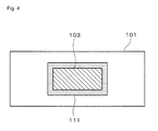
FIG. 4 is a diagram explaining the method for manufacturing an ESD protection device according to the example of the present invention, and a diagram illustrating the step of applying a discharge auxiliary electrode paste onto the unfired sealing layer to form an unfired discharge auxiliary electrode; and -
FIG. 5 is a diagram explaining the method for manufacturing an ESD protection device according to the example of the present invention, and a diagram illustrating the step of applying an opposed electrode paste to form unfired opposed electrodes on one and the other sides. - With reference to an example of the present invention, features of the present invention will be described below in details.
-
FIG. 1 is a cross-sectional view schematically illustrating the structure of an ESD protection device according to an example of the present invention, andFIG. 2 is a plan view of the ESD protection device according to the example of the present invention. - This ESD protection device includes, as shown in
FIGS. 1 and2 , aceramic base material 1 containing a glass component, opposedelectrodes 2 of anopposed electrode 2a on one side and anopposed electrode 2b on the other side, which are formed on the surface of theceramic base material 1, and have ends opposed to each other, a dischargeauxiliary electrode 3 in partial contact with theopposed electrode 2a on one side and theopposed electrode 2b on the other side, which is formed so as to provide a bridge from theopposed electrode 2a on one side to theopposed electrode 2b on the other side, andexternal electrodes ceramic base material 1 to provide conduction to theopposed electrode 2a on one side and theopposed electrode 2b on the other side for constituting theopposed electrodes 2. - The discharge
auxiliary electrode 3 includes metallic particles and a ceramic component, which is configured to reduce excessive sintering of the dischargeauxiliary electrode 3, thereby making it possible to prevent short circuit detects from being caused by excessive sintering. - It is possible to use, as the metallic particles, copper particles, and preferably, a copper powder with a surface coated with an inorganic oxide or a ceramic component. In addition, while the ceramic component is not particularly limited, more preferable ceramic components include, as an example, a ceramic component containing the constitution material of the ceramic base material (in this case, a Ba-Si-Al based material), or a ceramic component containing a semiconductor component such as SiC.
- Furthermore, in this ESD protection device, a sealing
layer 11 is placed between the dischargeauxiliary electrode 3 and theceramic base material 1. - This
sealing layer 11 is a porous layer composed of, for example, ceramic grains such as alumina, which functions to absorb and keep (trap) the glass component contained in theceramic base material 1 and the glass component produced in theceramic base material 1 in a firing step to suppress and prevent the ingress of the glass component into the dischargeauxiliary electrode 3, thereby preventing short circuit detects from being caused by excessive sintering of the discharge auxiliary electrode section. - It is to be noted that he ESD protection device according to this example has the sealing
layer 11 placed over a wide range so as to be interposed not only between the dischargeauxiliary electrode 3 and theceramic base material 1, but also between theceramic base material 1 and connections between theopposed electrodes 2 and the dischargeauxiliary electrode 3, and the ESD protection device is thus configured so that the ingress of the glass component into the connections is also suppressed and prevented accordingly. - A method will be described below for manufacturing an ESD protection device which has the structure as described above.
- Materials containing Ba, Al, and Si as main constituents are prepared as ceramic materials for the material of the
ceramic base material 1. - Then, the respective materials are blended to provide a predetermined composition, and subjected to calcination at 800°C to 1000°C. The calcined powder obtained is subjected to grinding in a zirconia ball mill for 12 hours to obtain a ceramic powder.
- This ceramic powder with an organic solvent such as toluene or ekinen added is mixed, followed by the further addition and mixing of a binder and a plasticizer, thereby preparing a slurry.
- This slurry is subjected to shape forming by a doctor blade method, thereby preparing a ceramic green sheet with a thickness of 50 µm.
- In addition, as an opposed electrode paste for forming the pair of
opposed electrodes - Furthermore, as a discharge auxiliary electrode paste for forming the discharge
auxiliary electrode 3, a Cu powder with a surface coated with 5 weight% of aluminum oxide and with an average particle size of approximately 3 µm, a silicon carbide powder with an average particle size of approximately 0.5 µm, and an organic vehicle including ethyl cellulose and terpineol are blended, and agitated and mixed with the use of a three roll mill to prepare a discharge auxiliary electrode paste. - It is to be noted that the mixture ratio of the Cu powder to the silicon carbide powder was adjusted to be 80/20 in terms of volume ratio.
- In this example, multiple types of pastes each containing an inorganic oxide and an organic vehicle were prepared as sealing layer pastes.
- It is to be noted that it is desirable in the present invention to use a sealing layer paste which has a difference ΔB (= B1 - B2) of 1.4 or less between the basicity B1 of the sealing layer paste as a main constituent material and the basicity B2 of an amorphous portion of the ceramic base material, and in this example, inorganic oxides M1 to M10 were used as the main constituent of the sealing layer paste (sealing layer main constituent) as shown in Table 1.
- In addition, as the organic vehicle, an organic vehicle OV1 was used in which resins P1 and P2 shown in Table 2 and a solvent (terpineol) were blended at the ratio as shown in Table 3.
[Table 1] Sample Number Sealing Layer Main Constituent B value ΔB value Melting Point M1 BaO 1.443 1.33 1923 M2 CaO 1.000 0.89 2572 M3 Al2O3 0.191 0.08 2054 M4 Nb2O5 0.022 -0.09 1520 M5 TiO2 0.125 0.02 1855 M6 ZrO2 0.183 0.07 2715 M7 CeO2 0.255 0.15 340 M8 MgO 0.638 0.53 2800 M9 ZnO 0.721 0.61 1975 M10 SrO 1.157 1.05 2430 [Table 2] Sample Number Resin Type Resin Weight Average Molecular Weight P1 Ethocel Resin 5 × 10⁴ P2 Alkyd Resin 8 × 10³ [Table 3] Sample Number Resin Solvent P1 P2 Terpineol OV1 9 4.5 86.5 - However, the type of the sealing layer main constituent, the method for manufacturing the sealing layer constituent, etc. have no particular limitations. For example, the grain size of M3 (Al2O3) in Table 1 was varied within the range of D50 = 0.2 to 2.5 µm to evaluate the characteristics, and it has been confirmed that the characteristics are not affected. In addition, it has been confirmed that the characteristics are also not affected in the evaluation of using varying M3 in regard to the manufacturing method. It is to be noted that the sealing layer main constituent was used on the order of D50 = 0.4 to 0.6 µm in this example.
- The basicity of an oxide melt can be classified broadly into an average oxygen ionic activity (conceptual basicity) obtained by calculation from the composition of the system in question, or an oxygen ionic activity (action point basicity) obtained by measurement of a response to externally provided stimulation such as a chemical reaction (redox potential measurement, optical spectrum measurement, etc.).
- It is desirable to use the conceptual basicity in the case of using the basicity for research on the nature or structure of, or as a compositional parameter of an oxide melt. On the other hand, various phenomena involving an oxide melt are organized by the action point basicity in a more suitable manner. The basicity in the present application refers to the former conceptual basicity.
- More specifically, the Mi-O bonding strength of the oxide (inorganic oxide) MiO can be expressed by the attraction between the cation and the oxygen ion, which is represented by the following formula (1).

Ai: cation-oxygen ion attraction, Zi : valence of i component cation, ri : radius of i component cation (Å) - The oxygen donation ability of the single component oxide MiO is provided by the reciprocal of Ai, and thus satisfies the following formula (2).

- Now, in order to deal with the oxygen donation ability ideologically and quantitatively, the obtained Bi0 value is turned into an indicator.
- The Bi 0 value obtained above from the formula (2) is substituted into the following formula (3) to recalculate the basicity, thereby making it possible to deal with the basicity quantitatively for all of the oxides.

- It is to be noted that when Bi 0 value is turned into an indicator, the Bi value of CaO and the Bi value of SiO2 are respectively defined as 1.000 (Bi 0 = 1.43) and 0.000 (Bi 0 = 0.41).
- The respective inorganic oxides M1 to M10 shown in Table 1 and the organic vehicle OV1 of composition as shown in Table 3 were blended at ratios as shown in Table 4, and kneaded and dispersed with the use of a three roll mill or the like to prepare sealing layer pastes P1 to P10 as shown in Table 4.
[Table 4] Sample Number Constituent of Sealing Layer (volume%) Organic Vehicle M1 M2 M3 M4 M5 M6 M7 M8 M9 M10 OV P1 18.8 - - - - - - - - - 81.2 P2 - 18.8 - - - - - - - - 81.2 P3 - - 18.8 - - - - - - - 81.2 P4 - - - 18.8 - - - - - - 81.2 P5 - - - - 18.8 - - - - - 81.2 P6 - - - - - 18.8 - - - - 81.2 P7 - - - - - - 18.8 - - - 81.2 P8 - - - - - - - 18.8 - - 81.2 P9 - - - - - - - - 18.8 - 81.2 P10 - - - - - - - - - 18.8 81.2 - First, as shown in
FIG. 3 , the sealing layer paste is applied onto the first ceramicgreen sheet 101 to form theunfired sealing layer 111. - Then, as shown in
FIG. 4 , the discharge auxiliary electrode paste is printed on theunfired sealing layer 111 by a screen printing method so as to provide a predetermined pattern, thereby forming the unfired dischargeauxiliary electrode 103. - Furthermore, as shown in
FIG. 5 , the opposed electrode paste is applied to form the unfiredopposed electrodes FIGS. 1 and2 ) after firing. Thus, agap section 110 corresponding to a discharge gap section 10 (FIGS. 1 and2 ) is formed between the ends of the unfiredopposed electrodes - It is to be noted that the width W of the
opposed electrodes discharge gap 10 were respectively adjusted to be 100 µm and 30 µm at the stage after firing in this example. - It is to be noted that the respective pastes, including the sealing layer paste, may be applied directly onto an object onto which the pastes are to be applied, or may be applied by other methods such as a transfer method.
- In addition, the order of applying the respective pastes and the specific patterns of the pastes are not to be considered limited to the examples described above. However, it is always necessary to place the opposed electrodes and the discharge auxiliary electrode adjacent to each other. Furthermore, it is necessary to adopt a structure in which the sealing layer is placed between the ceramic constituting the ceramic base material and the electrode.
- A plurality of second ceramic green sheets with no paste applied thereto were stacked on the non-printing surface of first ceramic green sheet with the respective pastes applied thereto in the order of sealing layer paste, discharge auxiliary electrode paste, and opposed electrode paste in the way described above, and pressure bonding was carried out to form a laminated body. It is to be noted that the laminated body was formed so as to have a thickness of 0.3 mm after firing in this case.
- The laminated body obtained was cut into a predetermined size, and then subjected to firing under the condition of the maximum temperature of 980°C to 1000°C in a firing furnace with an atmosphere controlled by using N2/H2/H2O. Then, an external electrode paste was applied onto both ends of the fired chip (sample), and further subjected to firing in a firing furnace with an atmosphere controlled, thereby providing an ESD protection device with the structure as shown in
FIGS. 1 and2 . - Further, in this example, for the purpose of characteristic evaluation, the sealing layer pastes P1 to P10 shown in Table 4 were used as the sealing layer paste to prepare ESD protection devices (samples of
sample numbers 1 to 10 in Table 5) each including a sealing layer. - In addition, for comparison, an ESD protection device (a sample of
sample number 11 in Table 5) including no sealing layer was prepared. - Further, although not described in the present embodiment, for the purpose of improving weatherability, a protective film may be formed over the discharge gaps of the ESD protection devices after firing. While the material of the protective film is not to be considered particularly limited, examples of the material can include, for example, a material composed of an oxide powder such as alumina or silica and a thermosetting resin such as a thermosetting epoxy resin or a thermosetting silicone resin.
[Table 5] Sample Number Sealing Layer Paste P1 P2 P3 P4 P5 P6 P7 P8 P9 P10 1 ○ - - - - - - - - - 2 - ○ - - - - - - - - 3 - - ○ - - - - - - - 4 - - - ○ - - - - - - 5 - - - - ○ - - - - - 6 - - - - - ○ - - - - 7 - - - - - - ○ - - - 8 - - - - - - - ○ - - 9 - - - - - - - - ○ - 10 - - - - - - - - - ○ *11 3 * mark: outside the scope of the present invention (without the sealing layer) - Next, the respective ESD protection devices (samples) prepared in the way described above were examined for their respective characteristics by the following methods.
- The samples were cut along the thickness direction, the cut surfaces were subjected to polishing, the interface between the sealing layer and the ceramic base material was then observed by SEM and WDX to check the thickness of a reactive layer formed at the interface.
- Voltages were applied to the respective samples under two types of conditions of 8 kV × 50 shots and 20 kV × 10 shots, and the sample with log IR > 6 Ω was evaluated as a sample with good short circuit characteristics (O), whereas the sample with log IR ≤ 6 Q once during the continuous application of the voltage was evaluated as a sample with defective circuit characteristics (×).
- In conformity with the IEC standard, IEC 61000-4-2, a peak voltage value: Vpeak and a voltage value after 30 ns from the crest value: Vclamp were measured in the case of contact discharge at 8 kV. The voltage application was carried out 20 times for each sample.
- The sample with Vpeak_max ≤ 900 V was evaluated as a sample with good Vpeak (○), and the sample with Vclamp_max ≤ 100 V was evaluated as a sample with good Vclamp (○).
- Loads of short: 8 kV × 100 shots and Vclamp: 8 kV × 1000 shots were applied, and the sample with log IR > 6 and Vclamp_max ≤ 100 V for all of the measurement results was evaluated as a sample with good repetition characteristics (○).
- The appearances of the fired products were observed visually, furthermore, the products with their cross sections polished were observed under a microscope, and the sample with no crack caused was evaluated as a good sample (○). In addition, as for substrate warpage, the products were placed on a horizontal plate, and the sample with the center or ends not away from the plate was a good sample (○). Table 6 shows the results of evaluating the characteristics as described above.
[Table 6] Sample Number ΔB Thickness of Reactive Layer (µm) Short Circuit Characteristics V peak V clamp Repetition Characteristics Substrate Fracture, Substrate Warpage Comprehensive Evaluation 8 kV 20 kV 1 1.33 43.6 ○ ○ ○ ○ ○ ○ ○ 2 0.89 5.1 ○ ○ ○ ○ ○ ○ ○ 3 0.08 1.9 ○ ○ ○ ○ ○ ○ ○ 4 -0.09 1.6 ○ ○ ○ ○ ○ ○ ○ 5 0.02 4.2 ○ ○ ○ ○ ○ ○ ○ 6 0.07 2.0 ○ ○ ○ ○ ○ ○ ○ 7 0.15 1.6 ○ ○ ○ ○ ○ ○ ○ 8 0.53 5.1 ○ ○ ○ ○ ○ ○ ○ 9 0.61 6.0 ○ ○ ○ ○ ○ ○ ○ 10 1.05 30.8 ○ ○ ○ ○ ○ ○ ○ *11 - - ○ × ○ ○ × ○ × 7 * mark: outside the scope of the present invention (without the sealing layer) - First, as for the thickness of the reactive layer, as shown in Table 6, it has been confirmed that the respective samples of
sample numbers 1 to 10 show a correlation between the ΔB value (see Table 1) and the thickness of the reactive layer, and there is a tendency that the thickness of the reactive layer is increased with increase in ΔB value. - Further, for the samples of
sample numbers 1 to 10 (that is, the samples with ΔB of 1.4 or less), it has been confirmed that sufficient adhesion is ensured at the interface between the sealing layer and the ceramic constituting the ceramic base material, and the samples are usable even when the firing temperature is lower than the melting point of the material constituting the sealing layer. - It is to be noted that no reactive layer was confirmed in the sample of
sample number 11 with no sealing layer provided. - As for short circuit characteristics, it has been confirmed that the respective samples of
sample numbers 1 to 10 have no short circuit defect caused after applying each of the initial short and the continuous ESD, and have no problem with their short circuit characteristics. - On the other hand, in the case of the sample of
sample number 11 with no sealing layer provided, it has been confirmed that the incidence of short circuit is increased as the inserted voltage value is increased, although no short circuit defect was caused in the evaluation at 8 kV. This is believed to be due to an increase in the inflow of the glass component from the ceramic into the discharge auxiliary electrode, and thus excessive sintering of the discharge auxiliary electrode, because of the sample ofsample number 11 including no sealing layer. - It is to be noted that the excessive sintering of the discharge auxiliary electrode brings the Cu powders close to each other, and thus makes it likely to cause a short circuit defect through fusion of the Cu powders to each other during the ESD application.
- In addition, it has been confirmed that each sample of
sample numbers 1 to 11 achieves required characteristics for Vpeak and Vclamp, and a discharge phenomenon is thus produced in the protection element quickly during the ESD application. - Furthermore, the following finding has been provided for the repetition characteristics. More specifically, it has been confirmed in each sample of
sample numbers 1 to 10 that the discharge capacity is kept favorable even when the frequency of voltage application is increased. - However, in the case of the sample of
sample number 11 including no sealing layer, short circuit caused was observed during the continuous application as for the short circuit characteristics, while required characteristics were achieved for Vpeak and Vclamp. - In addition, as for substrate fracture and substrate warpage, as shown in Table 6, it has been confirmed that either substrate fracture or substrate warpage is not caused when ΔB (the difference ΔB between the basicity B1 of the main constituent constituting the sealing layer and the basicity B2 of the amorphous portion of the ceramic constituting the ceramic base material) is 1.33 or less, in each case of the sealing layer using the material containing some of the elements constituting the ceramic substrate, and the sealing layer using the other materials shown in Table 1. Further, it has been confirmed from behaviors of other samples, not shown in Table 6, regarding substrate fracture and substrate warpage, etc. that favorable sealing layers can be formed without problems such as structural disorder as long as ΔB is 1.4 or less.
- To summarize the results in the example described above, it has been confirmed that according to the present invention, ESD protection devices are achieved which produce specific effects such as the following:
- (a) the sealing layer placed between the discharge auxiliary electrode and the ceramic base material can trap the glass component which tries to cause the ingress from the ceramic base material into the discharge auxiliary electrode, thereby preventing short circuit defects from being caused by excessive sintering of the discharge auxiliary electrode;
- (b) the reactive layer including a reaction product formed by the reaction between the constituent material of the sealing layer and the constituent material of the ceramic base material is formed at the interface between the sealing layer and the ceramic base material, thereby ensuring the adhesion between the sealing layer and the ceramic base material, and thus improving the reliability; and
- (c) the design is made so as to provide a difference ΔB (= B1 - B2) of 1.4 or less between the basicity B1 of the main constituent material of the sealing layer and the basicity B2 of the amorphous portion constituting the ceramic base material, thereby suppressing an excessive reaction between the sealing layer and the ceramic base material, and as a result, making it possible to prevent excessive sintering of the discharge auxiliary electrode.
- In addition, ESD protection devices achieved according to the present invention have stable characteristics, which are less likely to be degraded, even if the static electricity is applied repeatedly. Thus, it is possible to apply the ESD protection devices widely used in the field of ESD protection devices for the protection of various appliances and devices including semiconductor devices.
- It is to be noted that the present invention is not to be considered limited to the example, and it is possible to find various applications of and make various modifications to the constituent material of, specific shapes of, and methods of formation of the sealing layer, opposed electrodes, and discharge auxiliary electrode, the composition of the glass-containing ceramic constituting the ceramic base material, etc., within the scope of the present invention.
Claims (7)
- An ESD protection device comprising: a ceramic base material including a glass component; opposed electrodes comprising an opposed electrode on one side and an opposed electrode on the other side, the opposed electrodes formed so as to oppose to each other at a distance therebetween on the surface of the ceramic base material; and a discharge auxiliary electrode connected to each of the opposed electrode on one side and the opposed electrode on the other side constituting the opposed electrodes, the discharge auxiliary electrode placed so as to provide a bridge from the opposed electrode on one side to the opposed electrode on the other side, wherein a sealing layer for preventing ingress of the glass component from the ceramic base material into the discharge auxiliary electrode is provided between the discharge auxiliary electrode and the ceramic base material.
- The ESD protection device according to claim 1, wherein a reactive layer including a reaction product formed by a reaction between a constituent material of the sealing layer and a constituent material of the ceramic base material is provided at the interface between the sealing layer and the ceramic base material.
- The ESD protection device according to claim 1 or 2, wherein the difference ΔB (= B1 - B2) is 1.4 or less between basicity B1 of a main constituent material of the sealing layer and basicity B2 of an amorphous portion constituting the ceramic base material.
- The ESD protection device according to any one of claims 1 to 3, wherein the sealing layer contains some of elements constituting the ceramic base material.
- The ESD protection device according to any one of claims 1 to 4, wherein the sealing layer contains an aluminum oxide as its main constituent.
- The ESD protection device according to any one of claims 1 to 6, wherein the discharge auxiliary electrode includes a metallic particle and a ceramic component.
- A method for manufacturing an ESD protection device, the method comprising the steps of: printing a sealing layer paste on one principal surface of a first ceramic green sheet, thereby forming an unfired sealing layer; printing a discharge auxiliary electrode paste to coat at least a portion of the sealing layer, thereby forming an unfired discharge auxiliary electrode; printing an opposed electrode paste on one principal surface of the first ceramic green sheet, thereby forming unfired opposed electrodes comprising an opposed electrode on one side and an opposed electrode on the other side, the opposed electrodes each partially covering the discharge auxiliary electrode, and the opposed electrodes placed at a distance therebetween; stacking a second ceramic green sheet on the other principal surface of the first ceramic green sheet, thereby forming an unfired laminated body; and firing the laminated body.
Applications Claiming Priority (1)
| Application Number | Priority Date | Filing Date | Title |
|---|---|---|---|
| JP2010218444A JP5649391B2 (en) | 2010-09-29 | 2010-09-29 | ESD protection device |
Publications (3)
| Publication Number | Publication Date |
|---|---|
| EP2437362A2 true EP2437362A2 (en) | 2012-04-04 |
| EP2437362A3 EP2437362A3 (en) | 2014-10-29 |
| EP2437362B1 EP2437362B1 (en) | 2018-01-03 |
Family
ID=44785509
Family Applications (1)
| Application Number | Title | Priority Date | Filing Date |
|---|---|---|---|
| EP11182914.9A Active EP2437362B1 (en) | 2010-09-29 | 2011-09-27 | ESD protection device and manufacturing method therefor |
Country Status (6)
| Country | Link |
|---|---|
| US (1) | US8773824B2 (en) |
| EP (1) | EP2437362B1 (en) |
| JP (1) | JP5649391B2 (en) |
| KR (1) | KR101254084B1 (en) |
| CN (1) | CN102437513B (en) |
| TW (1) | TWI487226B (en) |
Families Citing this family (8)
| Publication number | Priority date | Publication date | Assignee | Title |
|---|---|---|---|---|
| JP5088396B2 (en) * | 2010-05-20 | 2012-12-05 | 株式会社村田製作所 | ESD protection device and manufacturing method thereof |
| JP2013101911A (en) * | 2011-10-14 | 2013-05-23 | Tdk Corp | Electrostatic surge suppressor |
| TWI517227B (en) * | 2012-02-24 | 2016-01-11 | Amazing Microelectronic Corp | Planetary Discharge Microchannel Structure and Its Making Method |
| CN104521079B (en) | 2012-08-13 | 2016-09-28 | 株式会社村田制作所 | ESD protection device |
| CN104541418B (en) * | 2012-08-13 | 2016-09-28 | 株式会社村田制作所 | ESD protection device |
| WO2014199752A1 (en) | 2013-06-13 | 2014-12-18 | 株式会社 村田製作所 | Ceramic electronic component and method for manufacturing same |
| CN104600568B (en) * | 2015-02-12 | 2017-03-01 | 苏州晶讯科技股份有限公司 | A kind of ceramic electrostatic suppressor and preparation method thereof |
| WO2018062839A1 (en) * | 2016-09-29 | 2018-04-05 | 주식회사 아모텍 | Static electricity protection device, method for manufacturing same and portable electronic apparatus having same |
Citations (3)
| Publication number | Priority date | Publication date | Assignee | Title |
|---|---|---|---|---|
| JPH09266053A (en) | 1996-03-28 | 1997-10-07 | Mitsubishi Materials Corp | Chip type surge absorber and manufacturing method thereof |
| JP2001043954A (en) | 1999-07-30 | 2001-02-16 | Tokin Corp | Surge absorbing element and method of manufacturing the same |
| JP4434314B2 (en) | 2008-02-05 | 2010-03-17 | 株式会社村田製作所 | ESD protection device |
Family Cites Families (10)
| Publication number | Priority date | Publication date | Assignee | Title |
|---|---|---|---|---|
| JP2000077163A (en) * | 1998-08-28 | 2000-03-14 | Tokin Corp | Surface mount type surge absorbing element |
| JP4140173B2 (en) * | 2000-05-31 | 2008-08-27 | 三菱マテリアル株式会社 | Chip-type surge absorber and manufacturing method thereof |
| JP2002270457A (en) * | 2001-03-07 | 2002-09-20 | Murata Mfg Co Ltd | Conductive paste and ceramic electronic component |
| JP4479470B2 (en) * | 2004-11-05 | 2010-06-09 | 三菱マテリアル株式会社 | surge absorber |
| JP2008010278A (en) * | 2006-06-28 | 2008-01-17 | Mitsubishi Materials Corp | Surge absorber and method of manufacturing surge absorber |
| CN101542856B (en) * | 2007-05-28 | 2012-05-30 | 株式会社村田制作所 | Electrostatic Discharge Protection Device |
| KR101008309B1 (en) * | 2008-07-21 | 2011-01-13 | 조인셋 주식회사 | ESD Protection Device with Low Capacitance |
| EP2352211B1 (en) * | 2008-11-26 | 2017-12-20 | Murata Manufacturing Co. Ltd. | Esd protection device and manufacturing method thereof |
| WO2010067503A1 (en) * | 2008-12-10 | 2010-06-17 | 株式会社 村田製作所 | Esd protection device |
| EP2453536B1 (en) * | 2009-09-30 | 2019-02-06 | Murata Manufacturing Co., Ltd. | Esd protection device and manufacturing method thereof |
-
2010
- 2010-09-29 JP JP2010218444A patent/JP5649391B2/en active Active
-
2011
- 2011-09-22 TW TW100134217A patent/TWI487226B/en active
- 2011-09-27 EP EP11182914.9A patent/EP2437362B1/en active Active
- 2011-09-27 CN CN201110306720.7A patent/CN102437513B/en active Active
- 2011-09-27 KR KR1020110097340A patent/KR101254084B1/en active Active
- 2011-09-28 US US13/247,029 patent/US8773824B2/en active Active
Patent Citations (3)
| Publication number | Priority date | Publication date | Assignee | Title |
|---|---|---|---|---|
| JPH09266053A (en) | 1996-03-28 | 1997-10-07 | Mitsubishi Materials Corp | Chip type surge absorber and manufacturing method thereof |
| JP2001043954A (en) | 1999-07-30 | 2001-02-16 | Tokin Corp | Surge absorbing element and method of manufacturing the same |
| JP4434314B2 (en) | 2008-02-05 | 2010-03-17 | 株式会社村田製作所 | ESD protection device |
Also Published As
| Publication number | Publication date |
|---|---|
| EP2437362B1 (en) | 2018-01-03 |
| CN102437513B (en) | 2014-07-16 |
| CN102437513A (en) | 2012-05-02 |
| JP2012074269A (en) | 2012-04-12 |
| US20120250196A1 (en) | 2012-10-04 |
| KR20120033255A (en) | 2012-04-06 |
| TWI487226B (en) | 2015-06-01 |
| EP2437362A3 (en) | 2014-10-29 |
| US8773824B2 (en) | 2014-07-08 |
| TW201250977A (en) | 2012-12-16 |
| JP5649391B2 (en) | 2015-01-07 |
| KR101254084B1 (en) | 2013-04-12 |
Similar Documents
| Publication | Publication Date | Title |
|---|---|---|
| EP2453536B1 (en) | Esd protection device and manufacturing method thereof | |
| EP2447959B1 (en) | Esd protection device and method for manufacturing same | |
| EP2437362B1 (en) | ESD protection device and manufacturing method therefor | |
| KR101072673B1 (en) | Esd protection device | |
| KR101254212B1 (en) | Esd protection device | |
| KR101013017B1 (en) | Varistor | |
| KR100674385B1 (en) | Stacked Chip Varistors | |
| WO2012043534A1 (en) | Esd protection device and method of manufacturing thereof | |
| JP2005353845A (en) | Laminated chip varistor | |
| JP4262141B2 (en) | Multilayer chip varistor and manufacturing method thereof | |
| JP4683068B2 (en) | Multilayer chip varistor | |
| WO2013137032A1 (en) | Antistatic element | |
| KR20140046072A (en) | Esd protection device and method of manufacturing same | |
| EP4425513B1 (en) | Molar ratio of ba ti and si in the dielectrics layers for multilayer ceramic component | |
| JP5614563B2 (en) | Manufacturing method of ESD protection device | |
| EP4557333A1 (en) | Multilayer ceramic capacitor | |
| CN116525227A (en) | Multilayer piezoresistor |
Legal Events
| Date | Code | Title | Description |
|---|---|---|---|
| PUAI | Public reference made under article 153(3) epc to a published international application that has entered the european phase |
Free format text: ORIGINAL CODE: 0009012 |
|
| AK | Designated contracting states |
Kind code of ref document: A2 Designated state(s): AL AT BE BG CH CY CZ DE DK EE ES FI FR GB GR HR HU IE IS IT LI LT LU LV MC MK MT NL NO PL PT RO RS SE SI SK SM TR |
|
| AX | Request for extension of the european patent |
Extension state: BA ME |
|
| REG | Reference to a national code |
Ref country code: DE Ref legal event code: R079 Ref document number: 602011044678 Country of ref document: DE Free format text: PREVIOUS MAIN CLASS: H01T0004120000 Ipc: H01T0002020000 |
|
| PUAL | Search report despatched |
Free format text: ORIGINAL CODE: 0009013 |
|
| AK | Designated contracting states |
Kind code of ref document: A3 Designated state(s): AL AT BE BG CH CY CZ DE DK EE ES FI FR GB GR HR HU IE IS IT LI LT LU LV MC MK MT NL NO PL PT RO RS SE SI SK SM TR |
|
| AX | Request for extension of the european patent |
Extension state: BA ME |
|
| RIC1 | Information provided on ipc code assigned before grant |
Ipc: H01T 21/00 20060101ALI20140922BHEP Ipc: H01T 2/02 20060101AFI20140922BHEP Ipc: H01T 4/10 20060101ALI20140922BHEP |
|
| 17P | Request for examination filed |
Effective date: 20150423 |
|
| RBV | Designated contracting states (corrected) |
Designated state(s): AL AT BE BG CH CY CZ DE DK EE ES FI FR GB GR HR HU IE IS IT LI LT LU LV MC MK MT NL NO PL PT RO RS SE SI SK SM TR |
|
| RIN1 | Information on inventor provided before grant (corrected) |
Inventor name: SAWADA, ERIKO Inventor name: SUMI, TAKAHIRO Inventor name: ADACHI, JUN |
|
| GRAP | Despatch of communication of intention to grant a patent |
Free format text: ORIGINAL CODE: EPIDOSNIGR1 |
|
| INTG | Intention to grant announced |
Effective date: 20170714 |
|
| GRAS | Grant fee paid |
Free format text: ORIGINAL CODE: EPIDOSNIGR3 |
|
| GRAA | (expected) grant |
Free format text: ORIGINAL CODE: 0009210 |
|
| AK | Designated contracting states |
Kind code of ref document: B1 Designated state(s): AL AT BE BG CH CY CZ DE DK EE ES FI FR GB GR HR HU IE IS IT LI LT LU LV MC MK MT NL NO PL PT RO RS SE SI SK SM TR |
|
| REG | Reference to a national code |
Ref country code: GB Ref legal event code: FG4D |
|
| REG | Reference to a national code |
Ref country code: CH Ref legal event code: EP Ref country code: AT Ref legal event code: REF Ref document number: 961095 Country of ref document: AT Kind code of ref document: T Effective date: 20180115 |
|
| REG | Reference to a national code |
Ref country code: IE Ref legal event code: FG4D |
|
| REG | Reference to a national code |
Ref country code: DE Ref legal event code: R096 Ref document number: 602011044678 Country of ref document: DE |
|
| REG | Reference to a national code |
Ref country code: NL Ref legal event code: MP Effective date: 20180103 |
|
| REG | Reference to a national code |
Ref country code: LT Ref legal event code: MG4D |
|
| REG | Reference to a national code |
Ref country code: AT Ref legal event code: MK05 Ref document number: 961095 Country of ref document: AT Kind code of ref document: T Effective date: 20180103 |
|
| PG25 | Lapsed in a contracting state [announced via postgrant information from national office to epo] |
Ref country code: NL Free format text: LAPSE BECAUSE OF FAILURE TO SUBMIT A TRANSLATION OF THE DESCRIPTION OR TO PAY THE FEE WITHIN THE PRESCRIBED TIME-LIMIT Effective date: 20180103 |
|
| PG25 | Lapsed in a contracting state [announced via postgrant information from national office to epo] |
Ref country code: NO Free format text: LAPSE BECAUSE OF FAILURE TO SUBMIT A TRANSLATION OF THE DESCRIPTION OR TO PAY THE FEE WITHIN THE PRESCRIBED TIME-LIMIT Effective date: 20180403 Ref country code: LT Free format text: LAPSE BECAUSE OF FAILURE TO SUBMIT A TRANSLATION OF THE DESCRIPTION OR TO PAY THE FEE WITHIN THE PRESCRIBED TIME-LIMIT Effective date: 20180103 Ref country code: FI Free format text: LAPSE BECAUSE OF FAILURE TO SUBMIT A TRANSLATION OF THE DESCRIPTION OR TO PAY THE FEE WITHIN THE PRESCRIBED TIME-LIMIT Effective date: 20180103 Ref country code: HR Free format text: LAPSE BECAUSE OF FAILURE TO SUBMIT A TRANSLATION OF THE DESCRIPTION OR TO PAY THE FEE WITHIN THE PRESCRIBED TIME-LIMIT Effective date: 20180103 Ref country code: ES Free format text: LAPSE BECAUSE OF FAILURE TO SUBMIT A TRANSLATION OF THE DESCRIPTION OR TO PAY THE FEE WITHIN THE PRESCRIBED TIME-LIMIT Effective date: 20180103 Ref country code: CY Free format text: LAPSE BECAUSE OF FAILURE TO SUBMIT A TRANSLATION OF THE DESCRIPTION OR TO PAY THE FEE WITHIN THE PRESCRIBED TIME-LIMIT Effective date: 20180103 |
|
| PG25 | Lapsed in a contracting state [announced via postgrant information from national office to epo] |
Ref country code: BG Free format text: LAPSE BECAUSE OF FAILURE TO SUBMIT A TRANSLATION OF THE DESCRIPTION OR TO PAY THE FEE WITHIN THE PRESCRIBED TIME-LIMIT Effective date: 20180403 Ref country code: RS Free format text: LAPSE BECAUSE OF FAILURE TO SUBMIT A TRANSLATION OF THE DESCRIPTION OR TO PAY THE FEE WITHIN THE PRESCRIBED TIME-LIMIT Effective date: 20180103 Ref country code: SE Free format text: LAPSE BECAUSE OF FAILURE TO SUBMIT A TRANSLATION OF THE DESCRIPTION OR TO PAY THE FEE WITHIN THE PRESCRIBED TIME-LIMIT Effective date: 20180103 Ref country code: LV Free format text: LAPSE BECAUSE OF FAILURE TO SUBMIT A TRANSLATION OF THE DESCRIPTION OR TO PAY THE FEE WITHIN THE PRESCRIBED TIME-LIMIT Effective date: 20180103 Ref country code: IS Free format text: LAPSE BECAUSE OF FAILURE TO SUBMIT A TRANSLATION OF THE DESCRIPTION OR TO PAY THE FEE WITHIN THE PRESCRIBED TIME-LIMIT Effective date: 20180503 Ref country code: PL Free format text: LAPSE BECAUSE OF FAILURE TO SUBMIT A TRANSLATION OF THE DESCRIPTION OR TO PAY THE FEE WITHIN THE PRESCRIBED TIME-LIMIT Effective date: 20180103 Ref country code: GR Free format text: LAPSE BECAUSE OF FAILURE TO SUBMIT A TRANSLATION OF THE DESCRIPTION OR TO PAY THE FEE WITHIN THE PRESCRIBED TIME-LIMIT Effective date: 20180404 Ref country code: AT Free format text: LAPSE BECAUSE OF FAILURE TO SUBMIT A TRANSLATION OF THE DESCRIPTION OR TO PAY THE FEE WITHIN THE PRESCRIBED TIME-LIMIT Effective date: 20180103 |
|
| REG | Reference to a national code |
Ref country code: DE Ref legal event code: R097 Ref document number: 602011044678 Country of ref document: DE |
|
| PG25 | Lapsed in a contracting state [announced via postgrant information from national office to epo] |
Ref country code: EE Free format text: LAPSE BECAUSE OF FAILURE TO SUBMIT A TRANSLATION OF THE DESCRIPTION OR TO PAY THE FEE WITHIN THE PRESCRIBED TIME-LIMIT Effective date: 20180103 Ref country code: AL Free format text: LAPSE BECAUSE OF FAILURE TO SUBMIT A TRANSLATION OF THE DESCRIPTION OR TO PAY THE FEE WITHIN THE PRESCRIBED TIME-LIMIT Effective date: 20180103 Ref country code: IT Free format text: LAPSE BECAUSE OF FAILURE TO SUBMIT A TRANSLATION OF THE DESCRIPTION OR TO PAY THE FEE WITHIN THE PRESCRIBED TIME-LIMIT Effective date: 20180103 Ref country code: RO Free format text: LAPSE BECAUSE OF FAILURE TO SUBMIT A TRANSLATION OF THE DESCRIPTION OR TO PAY THE FEE WITHIN THE PRESCRIBED TIME-LIMIT Effective date: 20180103 |
|
| PLBE | No opposition filed within time limit |
Free format text: ORIGINAL CODE: 0009261 |
|
| STAA | Information on the status of an ep patent application or granted ep patent |
Free format text: STATUS: NO OPPOSITION FILED WITHIN TIME LIMIT |
|
| PG25 | Lapsed in a contracting state [announced via postgrant information from national office to epo] |
Ref country code: CZ Free format text: LAPSE BECAUSE OF FAILURE TO SUBMIT A TRANSLATION OF THE DESCRIPTION OR TO PAY THE FEE WITHIN THE PRESCRIBED TIME-LIMIT Effective date: 20180103 Ref country code: SK Free format text: LAPSE BECAUSE OF FAILURE TO SUBMIT A TRANSLATION OF THE DESCRIPTION OR TO PAY THE FEE WITHIN THE PRESCRIBED TIME-LIMIT Effective date: 20180103 Ref country code: SM Free format text: LAPSE BECAUSE OF FAILURE TO SUBMIT A TRANSLATION OF THE DESCRIPTION OR TO PAY THE FEE WITHIN THE PRESCRIBED TIME-LIMIT Effective date: 20180103 Ref country code: DK Free format text: LAPSE BECAUSE OF FAILURE TO SUBMIT A TRANSLATION OF THE DESCRIPTION OR TO PAY THE FEE WITHIN THE PRESCRIBED TIME-LIMIT Effective date: 20180103 |
|
| 26N | No opposition filed |
Effective date: 20181005 |
|
| PG25 | Lapsed in a contracting state [announced via postgrant information from national office to epo] |
Ref country code: SI Free format text: LAPSE BECAUSE OF FAILURE TO SUBMIT A TRANSLATION OF THE DESCRIPTION OR TO PAY THE FEE WITHIN THE PRESCRIBED TIME-LIMIT Effective date: 20180103 |
|
| PG25 | Lapsed in a contracting state [announced via postgrant information from national office to epo] |
Ref country code: MC Free format text: LAPSE BECAUSE OF FAILURE TO SUBMIT A TRANSLATION OF THE DESCRIPTION OR TO PAY THE FEE WITHIN THE PRESCRIBED TIME-LIMIT Effective date: 20180103 |
|
| REG | Reference to a national code |
Ref country code: CH Ref legal event code: PL |
|
| GBPC | Gb: european patent ceased through non-payment of renewal fee |
Effective date: 20180927 |
|
| REG | Reference to a national code |
Ref country code: BE Ref legal event code: MM Effective date: 20180930 |
|
| REG | Reference to a national code |
Ref country code: IE Ref legal event code: MM4A |
|
| PG25 | Lapsed in a contracting state [announced via postgrant information from national office to epo] |
Ref country code: LU Free format text: LAPSE BECAUSE OF NON-PAYMENT OF DUE FEES Effective date: 20180927 |
|
| PG25 | Lapsed in a contracting state [announced via postgrant information from national office to epo] |
Ref country code: IE Free format text: LAPSE BECAUSE OF NON-PAYMENT OF DUE FEES Effective date: 20180927 |
|
| PG25 | Lapsed in a contracting state [announced via postgrant information from national office to epo] |
Ref country code: CH Free format text: LAPSE BECAUSE OF NON-PAYMENT OF DUE FEES Effective date: 20180930 Ref country code: BE Free format text: LAPSE BECAUSE OF NON-PAYMENT OF DUE FEES Effective date: 20180930 Ref country code: FR Free format text: LAPSE BECAUSE OF NON-PAYMENT OF DUE FEES Effective date: 20180930 Ref country code: LI Free format text: LAPSE BECAUSE OF NON-PAYMENT OF DUE FEES Effective date: 20180930 |
|
| PG25 | Lapsed in a contracting state [announced via postgrant information from national office to epo] |
Ref country code: GB Free format text: LAPSE BECAUSE OF NON-PAYMENT OF DUE FEES Effective date: 20180927 |
|
| PG25 | Lapsed in a contracting state [announced via postgrant information from national office to epo] |
Ref country code: MT Free format text: LAPSE BECAUSE OF NON-PAYMENT OF DUE FEES Effective date: 20180927 |
|
| PG25 | Lapsed in a contracting state [announced via postgrant information from national office to epo] |
Ref country code: TR Free format text: LAPSE BECAUSE OF FAILURE TO SUBMIT A TRANSLATION OF THE DESCRIPTION OR TO PAY THE FEE WITHIN THE PRESCRIBED TIME-LIMIT Effective date: 20180103 |
|
| PG25 | Lapsed in a contracting state [announced via postgrant information from national office to epo] |
Ref country code: HU Free format text: LAPSE BECAUSE OF FAILURE TO SUBMIT A TRANSLATION OF THE DESCRIPTION OR TO PAY THE FEE WITHIN THE PRESCRIBED TIME-LIMIT; INVALID AB INITIO Effective date: 20110927 Ref country code: PT Free format text: LAPSE BECAUSE OF FAILURE TO SUBMIT A TRANSLATION OF THE DESCRIPTION OR TO PAY THE FEE WITHIN THE PRESCRIBED TIME-LIMIT Effective date: 20180103 |
|
| PG25 | Lapsed in a contracting state [announced via postgrant information from national office to epo] |
Ref country code: MK Free format text: LAPSE BECAUSE OF NON-PAYMENT OF DUE FEES Effective date: 20180103 |
|
| PGFP | Annual fee paid to national office [announced via postgrant information from national office to epo] |
Ref country code: DE Payment date: 20250919 Year of fee payment: 15 |