EP2437172B1 - RAM-SEU-Verfahren zur Fehlerberichtigung - Google Patents
RAM-SEU-Verfahren zur Fehlerberichtigung Download PDFInfo
- Publication number
- EP2437172B1 EP2437172B1 EP11178698.4A EP11178698A EP2437172B1 EP 2437172 B1 EP2437172 B1 EP 2437172B1 EP 11178698 A EP11178698 A EP 11178698A EP 2437172 B1 EP2437172 B1 EP 2437172B1
- Authority
- EP
- European Patent Office
- Prior art keywords
- data
- parity
- output
- logic
- bad
- Prior art date
- Legal status (The legal status is an assumption and is not a legal conclusion. Google has not performed a legal analysis and makes no representation as to the accuracy of the status listed.)
- Active
Links
Images

Classifications
-
- G—PHYSICS
- G06—COMPUTING OR CALCULATING; COUNTING
- G06F—ELECTRIC DIGITAL DATA PROCESSING
- G06F11/00—Error detection; Error correction; Monitoring
- G06F11/07—Responding to the occurrence of a fault, e.g. fault tolerance
- G06F11/08—Error detection or correction by redundancy in data representation, e.g. by using checking codes
- G06F11/10—Adding special bits or symbols to the coded information, e.g. parity check, casting out 9's or 11's
- G06F11/1008—Adding special bits or symbols to the coded information, e.g. parity check, casting out 9's or 11's in individual solid state devices
- G06F11/1048—Adding special bits or symbols to the coded information, e.g. parity check, casting out 9's or 11's in individual solid state devices using arrangements adapted for a specific error detection or correction feature
-
- G—PHYSICS
- G06—COMPUTING OR CALCULATING; COUNTING
- G06F—ELECTRIC DIGITAL DATA PROCESSING
- G06F11/00—Error detection; Error correction; Monitoring
- G06F11/07—Responding to the occurrence of a fault, e.g. fault tolerance
- G06F11/16—Error detection or correction of the data by redundancy in hardware
- G06F11/1666—Error detection or correction of the data by redundancy in hardware where the redundant component is memory or memory area
- G06F11/167—Error detection by comparing the memory output
Definitions
- the present invention is related to memory systems and in particular to redundant memory systems for mitigating the effect of single event upset (SEU).
- SEU single event upset
- Exemplary prior art redundant memory systems are disclosed in US 2004/0225928 and US 5905854 .
- EDAC error detection and correction
- the present invention provides an error detection and correction (EDAC) circuit for use in a redundant memory system, the EDAC circuit comprising: a first input for receiving first data and parity information stored by a first memory device; a second input for receiving second data and parity information stored by a second memory device; a first output for providing either the first data or the second data onto a data bus; first parity check logic that calculates whether parity is 'good' or 'bad' in the received first data and parity information; second parity check logic that calculates whether parity is 'good' or 'bad' in the received second data and parity information; and bit comparison logic that detects differences between the first data and the second data, characterised in that the bit comparison logic detects differences between the first parity information and the second parity information, and by: data select logic that selects either the first data or the second data for provision to the first output based on the calculated parity of the first data and the second data and the differences between the first data and the second data, and between the
- the present invention provides A method of reducing single event upset (SEU) errors in memory systems with an error detection and correction (EDAC) circuit, the method comprising: retrieving first data and parity information from a first memory device; retrieving second data and parity information from a second memory device, wherein the second data is redundant to the first data retrieved from the first memory device; calculating whether the parity of the first data is 'good' or 'bad' based on the retrieved first data and parity information; calculating whether the parity of the second data is 'good' or 'bad' based on the retrieved second data and parity information; and detecting differences between the first data the second data, the method being characterised by: detecting differences between the first parity information and the second parity information; selecting either the first data or the second data for provision to a data bus based on the calculated parity of the first data and the second data and the differences between the first data and the second data, and between the first parity information and the second parity information; detecting
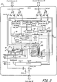
- FIG. 1 is a block diagram of a memory system having an error correction and detection (EDAC) circuit for mitigating single event upsets (SEUs) according to an embodiment of the present invention.
- EDAC error correction and detection
- FIG. 2 is a logic/block diagram illustrating operations performed by the EDAC according to an embodiment of the present invention.
- the present invention provides a memory system that mitigates the effect of single event upsets (SEUs).
- SEUs single event upsets
- the present invention employs redundant memory (e.g., first and second memory devices storing identical data) in combination with an error detection and correction (EDAC) circuit to mitigate the consequences of a SEU event.
- EDAC error detection and correction
- traditional EDAC circuits attempt to correct errant data by reconstructing the original data using error correction codes
- the EDAC circuit as described in greater detail herein performs correction by correctly selecting a redundant copy of the data. Storing redundant data ensures that even if an SEU event occurs on one of the memory devices, identical and presumably good data can be retrieved from the second memory.
- the function of the EDAC circuit is to identify when data on one or both of the redundant memories is 'bad', and select ⁇ good' data from the other memory to propagate to other systems.
- the EDAC circuit is responsible for recognizing when neither of the available data is 'good'.
- FIG. 1 is a block diagram of a memory system having an error correction and detection (EDAC) circuit for mitigating single event upsets (SEUs) according to an embodiment of the present invention.
- EDAC error correction and detection
- SEUs single event upsets
- memory system 10 is employed in an electronic engine control system for an aerospace application.
- the present invention may be applicable in a variety of applications, but is particularly suited for aerospace applications exposed to stray neutrons and other particles that are often associated with the presence of SEU errors.
- System 10 includes first processor 12, and second processor 14, first memory 16 (i.e., memory copy A), second memory 18 (i.e., memory copy B), error detection and correction (EDAC) circuit 20, oscillator 22, and low skew buffer 24.
- first and second processors 12 and 14 provide additional redundancy to the system, but in other embodiments a single processor (e.g., first processor 12) may be employed.
- First memory 16 and second memory 18 are redundant memory devices, meaning identical data is maintained in both devices.
- memory devices 16 and 18 are static random access memory (SRAM) devices, but other types of memory devices may be employed depending on the application.
- SRAM static random access memory
- EDAC circuit 20 is implemented with a field programmable gate array (FPGA) device, but in other embodiments may be implemented with a combination of various hardware and software components. Additionally, it will be understood that each of the first memory 16 and second memory 18 can include multiple memory devices, where one or more memory devices holding a first copy of data and parity information are referred to as first memory 16 or first memory device 16, and one or more memory devices holding a second copy of data and parity information are referred to as second memory 18 or second memory device 18.
- FPGA field programmable gate array
- First processor 12 includes external bus interface (EBI) 26 and phase lock loop (PLL) 28, with second processor 14 similarly including EBI 30 and PLL 32.
- EBIs 26 interface first processor 12 to second processor 14, first memory 16, second memory 18, and EDAC circuit 20 via control bus 34, address bus 36 and data bus 38, respectively.
- Control bus 34 communicates control instructions from first processor 12 (or second processor 14) to components such as the redundant memories 16 and 18, and EDAC circuit 20. Control instructions may include read commands, write commands, and test commands.
- Address bus 36 dictates the address to be accessed within the redundant memories 16 and 18.
- Data bus 38 communicates data to and from the redundant memories 16, 18 and EDAC circuit 20.
- Arbitration bus 40 is employed in embodiments relying on dual processors to determine which processor has priority over use of the control, address and data buses 34, 36, 38.
- Oscillator 22 provides a clock frequency for use in system 10.
- Low skew buffer 24 operates in conjunction with the system clock to distribute a synchronous clock signal to first processor 12, second processor 14, memory device 16, memory device 18 and EDAC circuit 20. In this way, synchronous communication is maintained between devices in memory system 10.
- memory system 10 The most common operations performed by memory system 10 are read/write operations. For example, to write data to memory first processor 12 (or second processor 14) places a 'write' command on control bus 34, an address identifying the location in memory data should be written to on address bus 36, and the data to be written on data bus 38. Commands/addresses/data placed on the respective buses 34, 36, 38 are communicated to both the first memory device 16 and second memory device 18. In this way, data placed on data bus 38 is written to both the first memory device 16 and second memory device 18, thereby maintaining redundant data in both devices.
- first processor 12 (or second processor 14) places a 'read' command on control bus 34 along with an address on address bus 36 that identifies the location in memory from which data should be read. Based on the received read command and address, the corresponding data is retrieved by both the first memory 16 and second memory 18 and communicated to EDAC circuit 20 for error detection and correction.
- EDAC circuit 20 checks for errors in the received data and makes a determination regarding which data to provide onto data bus 38 for readout by the respective processor. Operations performed by EDAC circuit 20 include identifying whether data from first memory 16 or second memory 18 have errors, what data is to be provided onto data bus 38, or whether the data is uncorrectable such that the system should be reset and default data should be provided onto data bus 38.
- FIG. 2 is a logic/block diagram illustrating operations performed by EDAC circuit 20 according to an embodiment of the present invention.
- EDAC circuit 20 encodes data (e.g., adding parity) used to identify errors during readback, determines whether the errors are correctable, selects data for output onto data bus 38, and determines when it is necessary to reset the memory system 12, 14, 16, 18, 20 of FIG. 1 .
- EDAC circuit 20 includes interfaces for bi-directional communication with first memory device 16, second memory device 18, and data bus 38.
- EDAC circuit 20 further includes a plurality of registers R1-R12 for capturing inputs and outputs provided to and from EDAC circuit 20, as well as for capturing internal data checks and comparisons within EDAC circuit 20.
- registers R1-R12 allow EDAC circuit 20 to pipeline the error detection and correction process.
- register R9 is used to latch data received from data bus 38 for subsequent provision to multiplexers 72 and 74, and parity generator 62. The data is subsequently latched along with generated parity bits by registers R1, R3, R5, and R7 for provision to the respective memory devices 16, 18. Similarly, data and parity bits read from the memory devices 16 and 18 are latched by registers R2, R4, R6, and R8, respectively.
- Additional registers R11 and R12 are employed within EDAC circuit 20 for storing the results of various comparisons and calculations associated with the error detection and correction functionality.
- EDAC circuit 20 operates to encode data received from data bus 38 with error correction bits that are subsequently used during read operations to determine whether the data is 'good' or 'bad'.
- EDAC circuit 20 employs parity generator 62 for appending parity bits to the received data. For each set of data bits, a parity bit is added to make the number of zeros or ones in the data either an even or an odd number. The parity bits are stored along with the data bits, and during readback the parity bits can be used to determine whether the data is 'good' or 'bad'.
- each data word is comprised of thirty-two bits divided into four 8-bit bytes.
- a parity bit is generated with respect to each 8-bit byte, resulting in four parity bits being associated with each thirty-two bit data word.
- the use of parity bits may result in simplified logic, reduced gate count, and increased throughput as compared to the use of more elaborate error correction codes or cyclic redundancy checks that can require more complex logic and/or additional clock cycles to complete.
- EDAC circuit 20 compares the data bits from both memories to one another to detect the number of bits that are different, checks the parity associated with each data word, and based on the results determines which copy of the data to use or whether neither copy of the data should be employed.
- the following table illustrates the behavior of EDAC circuit 20 as illustrated in FIG. 2 according to an embodiment of the present invention.
- the column 'Data Compare Output' is a function of a comparison of data bits from first memory 16 and second memory 18 that indicates the number of bits that are different between the respective data.
- the column 'Parity Compare Output' is a function of a comparison of parity A and parity B bits, with the output 'yes' indicating that no difference exists between the compared bits and 'no' indicating that a difference does exist between the parity bits.
- Cross-checking parity A bits and parity B bits provides increased error detection and accommodation coverage for faults in the check data in addition to handling errors in the data itself.
- the column 'Parity Check A Output' indicates the result of a parity check performed on the data word from first memory 16 based on the parity data from first memory 16.
- the column 'Copy to Use' indicates the memory from which data should be selected, and the column 'Reset' indicates whether neither set of data is 'good' such that the system 10 is reset.
- data A is selected to be provided to data bus 38. If there is a difference in the compared parity bits (but not in the compared data bits), indicating an error in either parity A bits or parity B bits, then EDAC circuit 20 selects data corresponding to whichever parity check comes out 'good' (rows 2, 3). That is, if the parity check for copy A is 'bad', then the error in the parity bits was likely in the parity A bits and therefore data B is provided to data bus 38.
- EDAC circuit 20 selects data based on which parity check indicates good parity (rows 4, 5). If neither the data comparison nor the parity comparison indicates any differences between the data provided by first memory 16 and second memory 18, but both parity checks are 'bad', this indicates a multiple-bit error between the data words, and neither copy of data is selected (row 6). In this instance, a reset signal is generated that indicates the system should be reset. In the event a single bit error is detected between data A and data B, as well as a difference between the parity bits, EDAC circuit 20 cannot determine which data copy is good and so default data is selected (row 7). Once again, a reset signal is generated indicating that the system should be reset. If a multiple bit error is detected between data A and data B, then EDAC circuit 20 selects default data and resets the system (row 8).
- Parity checker 50a receives the data word (labeled 'DataA') and parity bits (labeled 'ParityA') and performs a parity check to determine whether the parity is 'good'. In this way, parity checker 50a detects situations in which a single bit in the data is incorrect. In this embodiment, parity checker 50a checks the parity with respect to each 8-bit word and associated parity bit. In other embodiments, additional parity bits may be employed to improve the detection of errors.
- parity checker 50a determines that the parity of the data word is 'good', then the output ParChkA would indicate that all bytes within the data word is good (e.g., '0000').
- parity checker 50a determines that the parity of the first byte of the data word is 'bad', then the output would indicate an error in the first byte (e.g., '1000').
- the output of parity checker 50a is supplied to data select logic 54.
- Parity checker 50b performs the same function as that performed by parity checker 50a, but performs the parity check on data received from second memory device (e.g., data word labeled ⁇ DataB').
- the output of parity checker 50b (labeled ⁇ ParChkB') is supplied to single/multibit error status logic 56 and data select logic 54.
- single bit errors are detected by parity checker 50b, but multi-bit errors (within an individual byte of the data word) and errors within the parity bits are not detected.
- Bit compare logic 52 acts to compare the data word and parity bits from first memory device 16 to the data word and parity bits from second memory device 18. In this way, differences between individual bits can be detected.
- logic gate XOR1 compares data A from first memory 16 to data B from second memory 18 and generates an output (labeled 'Cmp_data') that identifies differences between the respective data words. If no errors exist, the data words stored in first memory 16 and second memory 18 are identical (i.e., redundant). If there are differences between the data words, those are indicated on a bit-by-bit basis in the bit compare output 'Cmp_data' provided to byte error detection logic 53 and single bit / multiple bit error detect logic 58.
- Logic gate XOR2 similarly compares parity bits from first memory 16 to parity bits from second memory 18 and generates an output (labeled 'Cmp_par') that identifies differences between the respective parity bits.
- the outputs provided by bit compare logic 52 are provided to both byte error detection logic 53 and to single bit/multiple bit error detection logic 58.
- Byte error detection logic 53 detects errors within the compared data and parity bits and provides an output indicating the bytes that contain errors to data select logic 54. Based on the received inputs, data select logic 54 selects either data A or data B. In one embodiment, in the event data select logic 54 determines that neither set of data is good, data A is nonetheless selected as a default. To select a particular copy of the data to be used, data select logic 54 provides a data select signal (e.g., DataSe10, DataSe11) to data multiplexer 70. Based on the received data select signal, data multiplexer 70 provides at its output the selected data (labeled 'Data_Out'). The selected data is registered by latch R10 and provided onto data bus 38 for readout by the processor.
- a data select signal e.g., DataSe10, DataSe11
- Byte error detection logic 53 cannot determine which copy of data or parity bits holds the error, only that a discrepancy exists between the compared bits.
- data select logic 54 selects the data word to provide onto data bus 38. For example, if no data errors or parity errors (i.e., discrepancies) are detected by byte error detection logic 53, then data select logic 54 selects by default data A provided by first memory 16 (Table 1, row 1). If errors are detected in the parity bits, but not in the data bits, then data select logic 54 selects data A if the parity check associated with data A is 'good' (row 2).
- data select logic 54 selects data B (row 3). If errors are detected in the data word, but not in the parity bits, then data select logic 54 selects the data A if the parity check associated with data A is 'good' (row 5). Otherwise data select logic 54 selects data B (row 6). If errors are detected in both the data bits and the parity bits, then data select logic 54 is unable to determine which copy of data is 'good', and therefore selects invalid data A with a system reset (row 7). Finally, if multiple bit errors are detected within the data word, then no information is valid and the EDAC circuit issues a system reset. (row 8).
- single bit/multiple bit error detect logic 58 includes XOR logic tree 60, AND logic tree 63, and AND logic tree 64 for determining whether a single or multiple bit error exists.
- the result of the data bit comparison provided by XOR1 is provided as an input to XOR logic tree 60 and AND logic tree 63.
- the result of the parity bit compare provided by XOR2 and the output of XOR logic tree 60 are combined by AND logic 64 to detect the presence of single bit/multiple bit errors that extend to the parity bits as well.
- single bit/multiple bit error detect logic 58 provides an indication to single/multibit error status logic 56 that determines whether, in the presence of multiple bit errors, the system 10 needs to be reset via the 'Reset' command.
- the memory devices 16, 18 may be rewritten, erased, or powered down and copied over with new data.
- the address at which the errors occurred (as provided by address bus 36) is latched by address latch on error logic 58 and provided as an input to single/multi-bit error status logic 56.
- the location of the detected error is provided by single/multi-bit error status logic 56 as part of the EDAC status output provided to data multiplexer 70, and in turn provided onto data bus 38 for communication to the processor.
- software error injection logic 66 and software parity error injection logic 80 act to inject or insert errors into data stored by memory devices 16 and 18. During subsequent readout, the response by EDAC circuit 20 can be monitored to ensure the injected errors are properly identified and handled.
- software error injection logic 66 includes data A overwrite module 76, data B overwrite module 78, and multiplexers 72 and 74. Data provided by data bus 38 as part of a write operation is provided to data overwrite modules 76 and 78, and multiplexers 72 and 74.
- data stored in data overwrite modules 76 and 78 are ignored, and the correct data is selected via multiplexers 72 and 74 for communication to memory devices 16 and 18, respectively.
- multiplexers 72 and 74 are configured to select data from data overwrite modules 76 and 78, respectively, for communication to memory devices 16 and 18, respectively.
- Data overwrite modules 76 and 78 can be controlled via control signals received from I/O decode processor interface 68 to modify the stored data, allowing software error injection module 66 to inject errors into the stored data (e.g., inject errors in one copy of the data to test the bit comparison function) before stored to memory devices 16 and 18.
- software parity error injection logic 80 allows errors to be injected into the parity bits prior to storage to memory devices 16 and 18.
- Software parity error injection module 80 likewise receives commands from I/O decode processor interface 68. In response, errors are selectively injected into one of the four bit positions for each data word. The injected error is combined by XOR logic 82 with the normally generated parity bits provided by parity generator 62 to generate the desired parity bits with injected errors for storage to memory devices 16 and 18.
- the present invention provides a system and method for detecting and correcting errors in a redundant memory system. While the invention has been described with reference to an exemplary embodiment(s), it will be understood by those skilled in the art that various changes may be made and equivalents may be substituted for elements thereof without departing from the scope of the invention. Therefore, it is intended that the invention not be limited to the particular embodiment(s) disclosed, but that the invention will include all embodiments falling within the scope of the appended claims.
Landscapes
- Engineering & Computer Science (AREA)
- Theoretical Computer Science (AREA)
- Quality & Reliability (AREA)
- Physics & Mathematics (AREA)
- General Engineering & Computer Science (AREA)
- General Physics & Mathematics (AREA)
- Techniques For Improving Reliability Of Storages (AREA)
Claims (8)
- Fehlerdetektions- und Korrekturschaltung (EDAC) (20) zum Gebrauch in einem redundanten Speichersystem (10), wobei die EDAC-Schaltung umfasst:einen ersten Eingang zum Entgegennehmen erster Daten- und Paritätsinformationen, die durch eine erste Speichervorrichtung (16) gespeichert sind;einen zweiten Eingang zum Entgegennehmen von zweiten Daten- und Paritätsinformationen, die durch eine zweite Speichervorrichtung (18) gespeichert sind,einen ersten Ausgang zum Liefern entweder der ersten Daten oder der zweiten Daten an einen Datenbus (38);eine erste Paritätsprüflogik (50a), die berechnet, ob die Parität in den entgegengenommenen ersten Daten- und Paritätsinformationen "gut" oder "schlecht" ist;eine zweite Paritätsprüflogik (50b), die berechnet, ob die Parität in den entgegengenommenen zweiten Daten- und Paritätsinformationen "gut" oder "schlecht" ist;eine Bitvergleichslogik (52), die Differenzen zwischen den ersten Daten und den zweiten Daten detektiert, wobei die Bitvergleichslogik Differenzen zwischen den ersten Paritätsinformationen und den zweiten Paritätsinformationen detektiert;eine Datenselektierungslogik (54), die entweder die ersten oder die zweiten Daten zur Lieferung an den ersten Ausgang selektiert, basierend auf der berechneten Parität der ersten Daten und der zweiten Daten und auf den Differenzen zwischen den ersten Daten und den zweiten Daten und zwischen den ersten Paritätsinformationen und den zweiten Paritätsinformationen,eine Einzelbit-/Multibit-Fehlerdetektionslogik (58), welche das Vorhandensein mehrfacher Bitfehler in den ersten und den zweiten Daten und Paritätsinformationen basierend auf den detektierten Differenzen zwischen den ersten Daten und den zweiten Daten und zwischen den ersten Paritätsinformationen und den zweiten Paritätsinformationen detektiert; undeine Einzelbit-/Multibit-Fehlerlogik (56), die das Speichersystem in Abhängigkeit von detektierten Mehrbitfehlern zurücksetzt,wobei das Verhalten der EDAC-Schaltung durch die folgende Tabelle bestimmt wird:
Fall Datenvergleichsausgang Paritätsvergleichsausgang Paritätsprüfungsausgang A Paritätsprüfungsausgang B Kopieren zur Verwendung Rücksetzen Normal - kein Fehler 0 Ja OK OK A Nein Einzelbitfehler in Parität B 0 Nein OK Schlechte gerade Parität A Nein ungerade Parität Einzelbitfehler in Parität A 0 Nein Schlechte gerade Parität OK B Nein ungerade Parität Einzelbitfehler in B 1 Ja OK Schlechte gerade Parität A Nein ungerade Parität Einzelbitfehler in A 1 Ja Schlechte gerade Parität OK B Nein ungerade Parität Mehrbitfehler 0 Ja Schlechte gerade Parität Schlechte gerade Parität Keiner Ja Mehrbitfehler 1 Nein Egal Egal Keiner Ja Mehrbitfehler 2-8 Egal Egal Egal Keiner Ja - EDAC-Schaltung nach Anspruch 1, ferner umfassend:eine eingebaute Testlogik (66) zum selektiven Injizieren von Fehlern in die dem ersten und dem zweiten Speicher gelieferten ersten bzw. zweiten Paritätsinformationen.
- EDAC-Schaltung nach Anspruch 2, wobei die eingebaute Testlogik selektiv Fehler in die dem ersten und dem zweiten Speicher gelieferten ersten bzw. zweiten Daten injiziert.
- Redundantes Speichersystem (10), umfassend:eine erste Speichervorrichtung (16) zum Speichern erster Daten und Paritätsinformationen;eine zweite Speichervorrichtung (18) zum Speichern zweiter Daten und Paritätsinformationen, welche gegenüber den ersten Daten und Paritätsinformationen redundant sind; undeine Fehlerdetektions- und Korrekturschaltung (EDAC) nach irgendeinem der vorstehenden Ansprüche,wobei die Fehlerdetektions- und Korrekturschaltung (EDAC) während Schreiboperationen Paritätsinformationen in Daten encodiert, die in die erste Speichervorrichtung und in die zweite Speichervorrichtung geschrieben werden, und während Leseoperationen bestimmt, ob Daten von der ersten Speichervorrichtung oder der zweiten Speichervorrichtung an einen Datenbus geliefert werden sollen.
- Redundantes Speichersystem nach Anspruch 4, wobei die erste und die zweite Speichervorrichtung einzelereignisempfindliche Vorrichtungen (SEU) sind.
- Verfahren zum Vermindern von Einzelereignisvorfall-Fehlern (SEU) in Speichersystemen (10) mit einer Fehlerdetektions- und Korrekturschaltung (EDAC) (20), wobei das Verfahren umfasst:Wiedergewinnen erster Daten- und Paritätsinformationen aus einer ersten Speichervorrichtung (16);Wiedergewinnen zweiter Daten- und Paritätsinformationen aus einer zweiten Speichervorrichtung (18), wobei die zweiten Daten redundant zu den ersten aus der ersten Speichervorrichtung wiedergewonnenen Daten sind;Berechnen, ob die Parität der ersten Daten "gut" oder "schlecht" ist, basierend auf den wiedergewonnenen ersten Daten und Paritätsinformationen;Berechnen, ob die Parität der zweiten Daten "gut" oder "schlecht" ist, basierend auf den wiedergewonnenen zweiten Daten und Paritätsinformationen;Detektieren von Differenzen zwischen den ersten Daten und den zweiten Daten;Detektieren von Differenzen zwischen den ersten Paritätsinformationen und den zweiten Paritätsinformationen;Selektieren entweder erster Daten oder zweiten Daten zur Lieferung an einen Datenbus (38), basierend auf der berechneten Parität der ersten Daten und der zweiten Daten sowie auf den Differenzen zwischen den ersten Daten und den zweiten Daten und zwischen den ersten Paritätsinformationen und den zweiten Paritätsinformationen;Detektieren des Vorhandenseins von multiplen Bitfehlern in den ersten und zweiten Daten und in Paritätsinformationen basierend auf den detektierten Differenzen zwischen den ersten Daten und den zweiten Daten und zwischen den ersten Paritätsinformationen und den zweiten Paritätsinformationen; undRücksetzen des Speichersystems in Abhängigkeit von detektierten multiplen Bitfehlern,wobei das Verhalten der EDAC-Schaltung durch die folgende Tabelle bestimmt ist:
Fall Datenvergleichsausgang Paritätsvergleichsausgang Paritätsprüfungsausgang A Paritätsprüfungsausgang B Kopieren zur Verwendung Rücksetzen Normal - kein Fehler 0 Ja OK OK A Nein Einzelbitfehler in Parität B 0 Nein OK Schlechte gerade Parität A Nein ungerade Parität Einzelbitfehler in Parität A 0 Nein Schlechte gerade Parität OK B Nein ungerade Parität Einzelbitfehler in B 1 Ja OK Schlechte gerade Parität A Nein ungerade Parität Einzelbitfehler in A 1 Ja Schlechte gerade Parität OK B Nein ungerade Parität Mehrbüfehler 0 Ja Schlechte gerade Parität Schlechte gerade Parität Keiner Ja Mehrbitfehler 1 Nein Egal Egal Keiner Ja Mehrbitfehler 2-8 Egal Egal Egal Keiner Ja - Verfahren nach Anspruch 6, ferner umfassend:Betreiben der EDAC-Schaltung in einem Testmodus, in welchem Fehler absichtlich in die mit den ersten und zweiten Daten verknüpften Paritätsinformationen injiziert werden; undÜberprüfen des Ausgangs der EDAC-Schaltung zum Bestimmen, ob die injizierten Fehler während des Auslesens der EDAC-Schaltung korrekt identifiziert worden sind.
- Verfahren nach Anspruch 6 oder 7, ferner umfassend
Betreiben der EDAC-Schaltung in einem Testmodus, in welchem Fehler absichtlich in die ersten und zweiten Daten injiziert werden; und
Überprüfen des Ausgangs der EDAC-Schaltung zum Bestimmen, ob die injizierten Fehler während des Auslesens durch die EDAC-Schaltung korrekt identifiziert worden sind.
Applications Claiming Priority (1)
| Application Number | Priority Date | Filing Date | Title |
|---|---|---|---|
| US12/896,348 US8589759B2 (en) | 2010-10-01 | 2010-10-01 | RAM single event upset (SEU) method to correct errors |
Publications (2)
| Publication Number | Publication Date |
|---|---|
| EP2437172A1 EP2437172A1 (de) | 2012-04-04 |
| EP2437172B1 true EP2437172B1 (de) | 2013-08-21 |
Family
ID=44677550
Family Applications (1)
| Application Number | Title | Priority Date | Filing Date |
|---|---|---|---|
| EP11178698.4A Active EP2437172B1 (de) | 2010-10-01 | 2011-08-24 | RAM-SEU-Verfahren zur Fehlerberichtigung |
Country Status (2)
| Country | Link |
|---|---|
| US (1) | US8589759B2 (de) |
| EP (1) | EP2437172B1 (de) |
Cited By (1)
| Publication number | Priority date | Publication date | Assignee | Title |
|---|---|---|---|---|
| US10896081B2 (en) | 2018-12-13 | 2021-01-19 | International Business Machines Corporation | Implementing SEU detection method and circuit |
Families Citing this family (23)
| Publication number | Priority date | Publication date | Assignee | Title |
|---|---|---|---|---|
| US8954806B2 (en) * | 2010-12-07 | 2015-02-10 | Cisco Technology, Inc. | Single event-upset controller wrapper that facilitates fault injection |
| US8589775B2 (en) * | 2011-03-14 | 2013-11-19 | Infineon Technologies Ag | Error tolerant flip-flops |
| WO2013101122A1 (en) * | 2011-12-29 | 2013-07-04 | Intel Corporation | Secure error handling |
| JP5910356B2 (ja) * | 2012-06-29 | 2016-04-27 | 富士通株式会社 | 電子装置、電子装置制御方法及び電子装置制御プログラム |
| US9229825B2 (en) | 2013-06-28 | 2016-01-05 | International Business Machines Corporation | Quick failover of blade server |
| KR102067040B1 (ko) * | 2014-04-23 | 2020-01-16 | 한국전자통신연구원 | 고장 방지 기능을 갖는 캐시 제어 장치 및 동작 방법 |
| US9575834B2 (en) | 2014-05-16 | 2017-02-21 | International Business Machines Corporation | Detecting single event upsets and stuck-at faults in RAM-based data path controllers |
| CN105093244A (zh) * | 2014-11-10 | 2015-11-25 | 航天恒星科技有限公司 | 一种gnss实时定轨系统和定轨方法 |
| JP6455168B2 (ja) * | 2015-01-16 | 2019-01-23 | 株式会社デンソー | メモリ装置システム |
| US10956265B2 (en) * | 2015-02-03 | 2021-03-23 | Hamilton Sundstrand Corporation | Method of performing single event upset testing |
| JP2017151785A (ja) * | 2016-02-25 | 2017-08-31 | ルネサスエレクトロニクス株式会社 | 半導体装置 |
| US10496484B2 (en) * | 2016-08-05 | 2019-12-03 | Sandisk Technologies Llc | Methods and apparatus for error detection for data storage devices |
| CN106844281A (zh) * | 2016-11-22 | 2017-06-13 | 北京控制工程研究所 | 一种适用于PowerPC处理器的高可靠指令Cache |
| US10635550B2 (en) * | 2017-12-08 | 2020-04-28 | Ge Aviation Systems Llc | Memory event mitigation in redundant software installations |
| US10452505B2 (en) * | 2017-12-20 | 2019-10-22 | Advanced Micro Devices, Inc. | Error injection for assessment of error detection and correction techniques using error injection logic and non-volatile memory |
| CN108763148B (zh) * | 2018-05-31 | 2021-11-30 | 西安微电子技术研究所 | 一种支持上注的容错存储器控制器 |
| WO2020005582A1 (en) | 2018-06-26 | 2020-01-02 | Rambus Inc. | Serializing and deserializing stage testing |
| US10949295B2 (en) | 2018-12-13 | 2021-03-16 | International Business Machines Corporation | Implementing dynamic SEU detection and correction method and circuit |
| CN110109619B (zh) * | 2019-04-25 | 2022-07-29 | 北京遥测技术研究所 | 一种闭环多级抗单粒子翻转效应的存储系统及实现方法 |
| CN112054784B (zh) * | 2019-06-05 | 2025-09-05 | 意法半导体国际有限公司 | 稳健软容错多位d触发器电路 |
| CN111597073B (zh) * | 2020-06-24 | 2021-08-03 | 上海安路信息科技股份有限公司 | Fpga单粒子翻转纠错方法及电路 |
| KR102379448B1 (ko) * | 2020-09-09 | 2022-03-29 | 주식회사에델테크 | 위성 데이터 처리 시스템에서 싱글 이벤트 이펙트를 처리하기 위한 장치 및 이를 이용한 방법 |
| CN114385410B (zh) * | 2022-01-12 | 2025-08-26 | 西安微电子技术研究所 | 一种prom程序存储区扩展edac校验电路及方法 |
Family Cites Families (11)
| Publication number | Priority date | Publication date | Assignee | Title |
|---|---|---|---|---|
| US5490155A (en) * | 1992-10-02 | 1996-02-06 | Compaq Computer Corp. | Error correction system for n bits using error correcting code designed for fewer than n bits |
| US5619642A (en) | 1994-12-23 | 1997-04-08 | Emc Corporation | Fault tolerant memory system which utilizes data from a shadow memory device upon the detection of erroneous data in a main memory device |
| US5574855A (en) | 1995-05-15 | 1996-11-12 | Emc Corporation | Method and apparatus for testing raid systems |
| US5872910A (en) | 1996-12-27 | 1999-02-16 | Unisys Corporation | Parity-error injection system for an instruction processor |
| JP4808839B2 (ja) | 2000-11-16 | 2011-11-02 | インヴェンサス・コーポレイション | メモリシステム |
| US6751756B1 (en) | 2000-12-01 | 2004-06-15 | Unisys Corporation | First level cache parity error inject |
| US7401269B2 (en) | 2003-05-10 | 2008-07-15 | Hewlett-Packard Development Company, L.P. | Systems and methods for scripting data errors to facilitate verification of error detection or correction code functionality |
| DE102006001873B4 (de) * | 2006-01-13 | 2009-12-24 | Infineon Technologies Ag | Vorrichtung und Verfahren zum Überprüfen einer Fehlererkennungsfunktionalität einer Speicherschaltung |
| JP4936746B2 (ja) * | 2006-03-08 | 2012-05-23 | ルネサスエレクトロニクス株式会社 | 半導体装置 |
| US7890836B2 (en) * | 2006-12-14 | 2011-02-15 | Intel Corporation | Method and apparatus of cache assisted error detection and correction in memory |
| US8627163B2 (en) | 2008-03-25 | 2014-01-07 | Micron Technology, Inc. | Error-correction forced mode with M-sequence |
-
2010
- 2010-10-01 US US12/896,348 patent/US8589759B2/en active Active
-
2011
- 2011-08-24 EP EP11178698.4A patent/EP2437172B1/de active Active
Cited By (1)
| Publication number | Priority date | Publication date | Assignee | Title |
|---|---|---|---|---|
| US10896081B2 (en) | 2018-12-13 | 2021-01-19 | International Business Machines Corporation | Implementing SEU detection method and circuit |
Also Published As
| Publication number | Publication date |
|---|---|
| US20120084628A1 (en) | 2012-04-05 |
| US8589759B2 (en) | 2013-11-19 |
| EP2437172A1 (de) | 2012-04-04 |
Similar Documents
| Publication | Publication Date | Title |
|---|---|---|
| EP2437172B1 (de) | RAM-SEU-Verfahren zur Fehlerberichtigung | |
| JP4071940B2 (ja) | メモリ設計のための共有式誤り訂正 | |
| US7587658B1 (en) | ECC encoding for uncorrectable errors | |
| US8185800B2 (en) | System for error control coding for memories of different types and associated methods | |
| US8352806B2 (en) | System to improve memory failure management and associated methods | |
| US9128868B2 (en) | System for error decoding with retries and associated methods | |
| CN107436821B (zh) | 为包括多个数据位和地址位的块生成错误码的装置和方法 | |
| US8176391B2 (en) | System to improve miscorrection rates in error control code through buffering and associated methods | |
| US20100287445A1 (en) | System to Improve Memory Reliability and Associated Methods | |
| US8181094B2 (en) | System to improve error correction using variable latency and associated methods | |
| US11126500B2 (en) | Error detection and correction with integrity checking | |
| US8918707B2 (en) | Codeword error injection via checkbit modification | |
| CN102356383B (zh) | 用于确定集成电路中的容错性的方法和系统 | |
| US9208027B2 (en) | Address error detection | |
| US8185801B2 (en) | System to improve error code decoding using historical information and associated methods | |
| US12081234B2 (en) | ECC memory chip encoder and decoder | |
| US12111726B2 (en) | Error rates for memory with built in error correction and detection | |
| US8707133B2 (en) | Method and apparatus to reduce a quantity of error detection/correction bits in memory coupled to a data-protected processor port | |
| US11069421B1 (en) | Circuitry for checking operation of error correction code (ECC) circuitry | |
| KR920010972B1 (ko) | 고장 방지 컴퓨터 메모리 시스템 | |
| US20260031176A1 (en) | Error detection, error correction or error detection and correction (edac) for electronic devices, electronic circuits or electronic systems | |
| US20250292862A1 (en) | Methodology to achieve transaction redundancy in memory constrained devices | |
| Wei | Design of External Memory Error Detection and Correction and Automatic Write-back | |
| CN118626307A (zh) | 数据结构、存储数据的纠错方法、模块、系统以及器件 |
Legal Events
| Date | Code | Title | Description |
|---|---|---|---|
| PUAI | Public reference made under article 153(3) epc to a published international application that has entered the european phase |
Free format text: ORIGINAL CODE: 0009012 |
|
| AK | Designated contracting states |
Kind code of ref document: A1 Designated state(s): AL AT BE BG CH CY CZ DE DK EE ES FI FR GB GR HR HU IE IS IT LI LT LU LV MC MK MT NL NO PL PT RO RS SE SI SK SM TR |
|
| AX | Request for extension of the european patent |
Extension state: BA ME |
|
| RIN1 | Information on inventor provided before grant (corrected) |
Inventor name: HARMAN, DAVID S. Inventor name: SENDLEIN, KIMBERLY K. Inventor name: GOSSE, JAMES A. Inventor name: COX, ROBERT E. |
|
| 17P | Request for examination filed |
Effective date: 20121004 |
|
| GRAP | Despatch of communication of intention to grant a patent |
Free format text: ORIGINAL CODE: EPIDOSNIGR1 |
|
| INTG | Intention to grant announced |
Effective date: 20130325 |
|
| GRAS | Grant fee paid |
Free format text: ORIGINAL CODE: EPIDOSNIGR3 |
|
| GRAA | (expected) grant |
Free format text: ORIGINAL CODE: 0009210 |
|
| AK | Designated contracting states |
Kind code of ref document: B1 Designated state(s): AL AT BE BG CH CY CZ DE DK EE ES FI FR GB GR HR HU IE IS IT LI LT LU LV MC MK MT NL NO PL PT RO RS SE SI SK SM TR |
|
| REG | Reference to a national code |
Ref country code: GB Ref legal event code: FG4D |
|
| REG | Reference to a national code |
Ref country code: CH Ref legal event code: EP |
|
| REG | Reference to a national code |
Ref country code: AT Ref legal event code: REF Ref document number: 628451 Country of ref document: AT Kind code of ref document: T Effective date: 20130915 |
|
| REG | Reference to a national code |
Ref country code: IE Ref legal event code: FG4D |
|
| REG | Reference to a national code |
Ref country code: DE Ref legal event code: R096 Ref document number: 602011002676 Country of ref document: DE Effective date: 20131017 |
|
| REG | Reference to a national code |
Ref country code: NL Ref legal event code: VDEP Effective date: 20130821 Ref country code: AT Ref legal event code: MK05 Ref document number: 628451 Country of ref document: AT Kind code of ref document: T Effective date: 20130821 |
|
| REG | Reference to a national code |
Ref country code: LT Ref legal event code: MG4D |
|
| PG25 | Lapsed in a contracting state [announced via postgrant information from national office to epo] |
Ref country code: HR Free format text: LAPSE BECAUSE OF FAILURE TO SUBMIT A TRANSLATION OF THE DESCRIPTION OR TO PAY THE FEE WITHIN THE PRESCRIBED TIME-LIMIT Effective date: 20130821 Ref country code: SE Free format text: LAPSE BECAUSE OF FAILURE TO SUBMIT A TRANSLATION OF THE DESCRIPTION OR TO PAY THE FEE WITHIN THE PRESCRIBED TIME-LIMIT Effective date: 20130821 Ref country code: LT Free format text: LAPSE BECAUSE OF FAILURE TO SUBMIT A TRANSLATION OF THE DESCRIPTION OR TO PAY THE FEE WITHIN THE PRESCRIBED TIME-LIMIT Effective date: 20130821 Ref country code: AT Free format text: LAPSE BECAUSE OF FAILURE TO SUBMIT A TRANSLATION OF THE DESCRIPTION OR TO PAY THE FEE WITHIN THE PRESCRIBED TIME-LIMIT Effective date: 20130821 Ref country code: CY Free format text: LAPSE BECAUSE OF FAILURE TO SUBMIT A TRANSLATION OF THE DESCRIPTION OR TO PAY THE FEE WITHIN THE PRESCRIBED TIME-LIMIT Effective date: 20130821 Ref country code: NO Free format text: LAPSE BECAUSE OF FAILURE TO SUBMIT A TRANSLATION OF THE DESCRIPTION OR TO PAY THE FEE WITHIN THE PRESCRIBED TIME-LIMIT Effective date: 20131121 Ref country code: IS Free format text: LAPSE BECAUSE OF FAILURE TO SUBMIT A TRANSLATION OF THE DESCRIPTION OR TO PAY THE FEE WITHIN THE PRESCRIBED TIME-LIMIT Effective date: 20131221 Ref country code: PT Free format text: LAPSE BECAUSE OF FAILURE TO SUBMIT A TRANSLATION OF THE DESCRIPTION OR TO PAY THE FEE WITHIN THE PRESCRIBED TIME-LIMIT Effective date: 20131223 |
|
| PG25 | Lapsed in a contracting state [announced via postgrant information from national office to epo] |
Ref country code: PL Free format text: LAPSE BECAUSE OF FAILURE TO SUBMIT A TRANSLATION OF THE DESCRIPTION OR TO PAY THE FEE WITHIN THE PRESCRIBED TIME-LIMIT Effective date: 20130821 Ref country code: BE Free format text: LAPSE BECAUSE OF FAILURE TO SUBMIT A TRANSLATION OF THE DESCRIPTION OR TO PAY THE FEE WITHIN THE PRESCRIBED TIME-LIMIT Effective date: 20130821 Ref country code: SI Free format text: LAPSE BECAUSE OF FAILURE TO SUBMIT A TRANSLATION OF THE DESCRIPTION OR TO PAY THE FEE WITHIN THE PRESCRIBED TIME-LIMIT Effective date: 20130821 Ref country code: FI Free format text: LAPSE BECAUSE OF FAILURE TO SUBMIT A TRANSLATION OF THE DESCRIPTION OR TO PAY THE FEE WITHIN THE PRESCRIBED TIME-LIMIT Effective date: 20130821 Ref country code: GR Free format text: LAPSE BECAUSE OF FAILURE TO SUBMIT A TRANSLATION OF THE DESCRIPTION OR TO PAY THE FEE WITHIN THE PRESCRIBED TIME-LIMIT Effective date: 20131122 Ref country code: LV Free format text: LAPSE BECAUSE OF FAILURE TO SUBMIT A TRANSLATION OF THE DESCRIPTION OR TO PAY THE FEE WITHIN THE PRESCRIBED TIME-LIMIT Effective date: 20130821 |
|
| PG25 | Lapsed in a contracting state [announced via postgrant information from national office to epo] |
Ref country code: CZ Free format text: LAPSE BECAUSE OF FAILURE TO SUBMIT A TRANSLATION OF THE DESCRIPTION OR TO PAY THE FEE WITHIN THE PRESCRIBED TIME-LIMIT Effective date: 20130821 Ref country code: EE Free format text: LAPSE BECAUSE OF FAILURE TO SUBMIT A TRANSLATION OF THE DESCRIPTION OR TO PAY THE FEE WITHIN THE PRESCRIBED TIME-LIMIT Effective date: 20130821 Ref country code: SK Free format text: LAPSE BECAUSE OF FAILURE TO SUBMIT A TRANSLATION OF THE DESCRIPTION OR TO PAY THE FEE WITHIN THE PRESCRIBED TIME-LIMIT Effective date: 20130821 Ref country code: DK Free format text: LAPSE BECAUSE OF FAILURE TO SUBMIT A TRANSLATION OF THE DESCRIPTION OR TO PAY THE FEE WITHIN THE PRESCRIBED TIME-LIMIT Effective date: 20130821 Ref country code: RO Free format text: LAPSE BECAUSE OF FAILURE TO SUBMIT A TRANSLATION OF THE DESCRIPTION OR TO PAY THE FEE WITHIN THE PRESCRIBED TIME-LIMIT Effective date: 20130821 Ref country code: NL Free format text: LAPSE BECAUSE OF FAILURE TO SUBMIT A TRANSLATION OF THE DESCRIPTION OR TO PAY THE FEE WITHIN THE PRESCRIBED TIME-LIMIT Effective date: 20130821 |
|
| REG | Reference to a national code |
Ref country code: IE Ref legal event code: MM4A |
|
| PG25 | Lapsed in a contracting state [announced via postgrant information from national office to epo] |
Ref country code: IT Free format text: LAPSE BECAUSE OF FAILURE TO SUBMIT A TRANSLATION OF THE DESCRIPTION OR TO PAY THE FEE WITHIN THE PRESCRIBED TIME-LIMIT Effective date: 20130821 Ref country code: ES Free format text: LAPSE BECAUSE OF FAILURE TO SUBMIT A TRANSLATION OF THE DESCRIPTION OR TO PAY THE FEE WITHIN THE PRESCRIBED TIME-LIMIT Effective date: 20130821 Ref country code: MC Free format text: LAPSE BECAUSE OF FAILURE TO SUBMIT A TRANSLATION OF THE DESCRIPTION OR TO PAY THE FEE WITHIN THE PRESCRIBED TIME-LIMIT Effective date: 20130821 |
|
| PLBE | No opposition filed within time limit |
Free format text: ORIGINAL CODE: 0009261 |
|
| STAA | Information on the status of an ep patent application or granted ep patent |
Free format text: STATUS: NO OPPOSITION FILED WITHIN TIME LIMIT |
|
| 26N | No opposition filed |
Effective date: 20140522 |
|
| PG25 | Lapsed in a contracting state [announced via postgrant information from national office to epo] |
Ref country code: IE Free format text: LAPSE BECAUSE OF NON-PAYMENT OF DUE FEES Effective date: 20130824 |
|
| REG | Reference to a national code |
Ref country code: DE Ref legal event code: R097 Ref document number: 602011002676 Country of ref document: DE Effective date: 20140522 |
|
| REG | Reference to a national code |
Ref country code: CH Ref legal event code: PL |
|
| PG25 | Lapsed in a contracting state [announced via postgrant information from national office to epo] |
Ref country code: LI Free format text: LAPSE BECAUSE OF NON-PAYMENT OF DUE FEES Effective date: 20140831 Ref country code: CH Free format text: LAPSE BECAUSE OF NON-PAYMENT OF DUE FEES Effective date: 20140831 |
|
| PG25 | Lapsed in a contracting state [announced via postgrant information from national office to epo] |
Ref country code: SM Free format text: LAPSE BECAUSE OF FAILURE TO SUBMIT A TRANSLATION OF THE DESCRIPTION OR TO PAY THE FEE WITHIN THE PRESCRIBED TIME-LIMIT Effective date: 20130821 |
|
| PG25 | Lapsed in a contracting state [announced via postgrant information from national office to epo] |
Ref country code: MT Free format text: LAPSE BECAUSE OF FAILURE TO SUBMIT A TRANSLATION OF THE DESCRIPTION OR TO PAY THE FEE WITHIN THE PRESCRIBED TIME-LIMIT Effective date: 20130821 Ref country code: TR Free format text: LAPSE BECAUSE OF FAILURE TO SUBMIT A TRANSLATION OF THE DESCRIPTION OR TO PAY THE FEE WITHIN THE PRESCRIBED TIME-LIMIT Effective date: 20130821 |
|
| PG25 | Lapsed in a contracting state [announced via postgrant information from national office to epo] |
Ref country code: BG Free format text: LAPSE BECAUSE OF FAILURE TO SUBMIT A TRANSLATION OF THE DESCRIPTION OR TO PAY THE FEE WITHIN THE PRESCRIBED TIME-LIMIT Effective date: 20130821 Ref country code: LU Free format text: LAPSE BECAUSE OF NON-PAYMENT OF DUE FEES Effective date: 20130824 Ref country code: RS Free format text: LAPSE BECAUSE OF FAILURE TO SUBMIT A TRANSLATION OF THE DESCRIPTION OR TO PAY THE FEE WITHIN THE PRESCRIBED TIME-LIMIT Effective date: 20131121 Ref country code: MK Free format text: LAPSE BECAUSE OF FAILURE TO SUBMIT A TRANSLATION OF THE DESCRIPTION OR TO PAY THE FEE WITHIN THE PRESCRIBED TIME-LIMIT Effective date: 20130821 Ref country code: HU Free format text: LAPSE BECAUSE OF FAILURE TO SUBMIT A TRANSLATION OF THE DESCRIPTION OR TO PAY THE FEE WITHIN THE PRESCRIBED TIME-LIMIT; INVALID AB INITIO Effective date: 20110824 |
|
| REG | Reference to a national code |
Ref country code: FR Ref legal event code: PLFP Year of fee payment: 6 |
|
| REG | Reference to a national code |
Ref country code: DE Ref legal event code: R082 Ref document number: 602011002676 Country of ref document: DE Representative=s name: SCHMITT-NILSON SCHRAUD WAIBEL WOHLFROM PATENTA, DE |
|
| REG | Reference to a national code |
Ref country code: FR Ref legal event code: PLFP Year of fee payment: 7 |
|
| REG | Reference to a national code |
Ref country code: FR Ref legal event code: PLFP Year of fee payment: 8 |
|
| PG25 | Lapsed in a contracting state [announced via postgrant information from national office to epo] |
Ref country code: AL Free format text: LAPSE BECAUSE OF FAILURE TO SUBMIT A TRANSLATION OF THE DESCRIPTION OR TO PAY THE FEE WITHIN THE PRESCRIBED TIME-LIMIT Effective date: 20130821 |
|
| P01 | Opt-out of the competence of the unified patent court (upc) registered |
Effective date: 20230522 |
|
| PGFP | Annual fee paid to national office [announced via postgrant information from national office to epo] |
Ref country code: DE Payment date: 20250724 Year of fee payment: 15 |
|
| PGFP | Annual fee paid to national office [announced via postgrant information from national office to epo] |
Ref country code: GB Payment date: 20250725 Year of fee payment: 15 |
|
| PGFP | Annual fee paid to national office [announced via postgrant information from national office to epo] |
Ref country code: FR Payment date: 20250725 Year of fee payment: 15 |