EP2434594B1 - Photonic integrated circuit for wavelength division multiplexing - Google Patents
Photonic integrated circuit for wavelength division multiplexing Download PDFInfo
- Publication number
- EP2434594B1 EP2434594B1 EP10290509.8A EP10290509A EP2434594B1 EP 2434594 B1 EP2434594 B1 EP 2434594B1 EP 10290509 A EP10290509 A EP 10290509A EP 2434594 B1 EP2434594 B1 EP 2434594B1
- Authority
- EP
- European Patent Office
- Prior art keywords
- converter
- waveguide
- wavelength
- transmitter
- converters
- Prior art date
- Legal status (The legal status is an assumption and is not a legal conclusion. Google has not performed a legal analysis and makes no representation as to the accuracy of the status listed.)
- Not-in-force
Links
Images
Classifications
-
- H—ELECTRICITY
- H01—ELECTRIC ELEMENTS
- H01S—DEVICES USING THE PROCESS OF LIGHT AMPLIFICATION BY STIMULATED EMISSION OF RADIATION [LASER] TO AMPLIFY OR GENERATE LIGHT; DEVICES USING STIMULATED EMISSION OF ELECTROMAGNETIC RADIATION IN WAVE RANGES OTHER THAN OPTICAL
- H01S5/00—Semiconductor lasers
- H01S5/06—Arrangements for controlling the laser output parameters, e.g. by operating on the active medium
- H01S5/062—Arrangements for controlling the laser output parameters, e.g. by operating on the active medium by varying the potential of the electrodes
- H01S5/0625—Arrangements for controlling the laser output parameters, e.g. by operating on the active medium by varying the potential of the electrodes in multi-section lasers
-
- G—PHYSICS
- G02—OPTICS
- G02B—OPTICAL ELEMENTS, SYSTEMS OR APPARATUS
- G02B6/00—Light guides; Structural details of arrangements comprising light guides and other optical elements, e.g. couplings
- G02B6/10—Light guides; Structural details of arrangements comprising light guides and other optical elements, e.g. couplings of the optical waveguide type
- G02B6/12—Light guides; Structural details of arrangements comprising light guides and other optical elements, e.g. couplings of the optical waveguide type of the integrated circuit kind
- G02B6/12007—Light guides; Structural details of arrangements comprising light guides and other optical elements, e.g. couplings of the optical waveguide type of the integrated circuit kind forming wavelength selective elements, e.g. multiplexer, demultiplexer
- G02B6/12009—Light guides; Structural details of arrangements comprising light guides and other optical elements, e.g. couplings of the optical waveguide type of the integrated circuit kind forming wavelength selective elements, e.g. multiplexer, demultiplexer comprising arrayed waveguide grating [AWG] devices, i.e. with a phased array of waveguides
-
- H—ELECTRICITY
- H01—ELECTRIC ELEMENTS
- H01S—DEVICES USING THE PROCESS OF LIGHT AMPLIFICATION BY STIMULATED EMISSION OF RADIATION [LASER] TO AMPLIFY OR GENERATE LIGHT; DEVICES USING STIMULATED EMISSION OF ELECTROMAGNETIC RADIATION IN WAVE RANGES OTHER THAN OPTICAL
- H01S5/00—Semiconductor lasers
- H01S5/02—Structural details or components not essential to laser action
- H01S5/026—Monolithically integrated components, e.g. waveguides, monitoring photo-detectors, drivers
- H01S5/0265—Intensity modulators
-
- H—ELECTRICITY
- H01—ELECTRIC ELEMENTS
- H01S—DEVICES USING THE PROCESS OF LIGHT AMPLIFICATION BY STIMULATED EMISSION OF RADIATION [LASER] TO AMPLIFY OR GENERATE LIGHT; DEVICES USING STIMULATED EMISSION OF ELECTROMAGNETIC RADIATION IN WAVE RANGES OTHER THAN OPTICAL
- H01S5/00—Semiconductor lasers
- H01S5/02—Structural details or components not essential to laser action
- H01S5/026—Monolithically integrated components, e.g. waveguides, monitoring photo-detectors, drivers
- H01S5/0268—Integrated waveguide grating router, e.g. emission of a multi-wavelength laser array is combined by a "dragon router"
-
- H—ELECTRICITY
- H01—ELECTRIC ELEMENTS
- H01S—DEVICES USING THE PROCESS OF LIGHT AMPLIFICATION BY STIMULATED EMISSION OF RADIATION [LASER] TO AMPLIFY OR GENERATE LIGHT; DEVICES USING STIMULATED EMISSION OF ELECTROMAGNETIC RADIATION IN WAVE RANGES OTHER THAN OPTICAL
- H01S5/00—Semiconductor lasers
- H01S5/10—Construction or shape of the optical resonator, e.g. extended or external cavity, coupled cavities, bent-guide, varying width, thickness or composition of the active region
- H01S5/12—Construction or shape of the optical resonator, e.g. extended or external cavity, coupled cavities, bent-guide, varying width, thickness or composition of the active region the resonator having a periodic structure, e.g. in distributed feedback [DFB] lasers
-
- H—ELECTRICITY
- H01—ELECTRIC ELEMENTS
- H01S—DEVICES USING THE PROCESS OF LIGHT AMPLIFICATION BY STIMULATED EMISSION OF RADIATION [LASER] TO AMPLIFY OR GENERATE LIGHT; DEVICES USING STIMULATED EMISSION OF ELECTROMAGNETIC RADIATION IN WAVE RANGES OTHER THAN OPTICAL
- H01S5/00—Semiconductor lasers
- H01S5/40—Arrangement of two or more semiconductor lasers, not provided for in groups H01S5/02 - H01S5/30
- H01S5/4025—Array arrangements, e.g. constituted by discrete laser diodes or laser bar
- H01S5/4031—Edge-emitting structures
-
- H—ELECTRICITY
- H01—ELECTRIC ELEMENTS
- H01S—DEVICES USING THE PROCESS OF LIGHT AMPLIFICATION BY STIMULATED EMISSION OF RADIATION [LASER] TO AMPLIFY OR GENERATE LIGHT; DEVICES USING STIMULATED EMISSION OF ELECTROMAGNETIC RADIATION IN WAVE RANGES OTHER THAN OPTICAL
- H01S5/00—Semiconductor lasers
- H01S5/40—Arrangement of two or more semiconductor lasers, not provided for in groups H01S5/02 - H01S5/30
- H01S5/4025—Array arrangements, e.g. constituted by discrete laser diodes or laser bar
- H01S5/4087—Array arrangements, e.g. constituted by discrete laser diodes or laser bar emitting more than one wavelength
-
- H—ELECTRICITY
- H04—ELECTRIC COMMUNICATION TECHNIQUE
- H04B—TRANSMISSION
- H04B10/00—Transmission systems employing electromagnetic waves other than radio-waves, e.g. infrared, visible or ultraviolet light, or employing corpuscular radiation, e.g. quantum communication
- H04B10/50—Transmitters
- H04B10/572—Wavelength control
-
- H—ELECTRICITY
- H04—ELECTRIC COMMUNICATION TECHNIQUE
- H04J—MULTIPLEX COMMUNICATION
- H04J14/00—Optical multiplex systems
- H04J14/02—Wavelength-division multiplex systems
Definitions
- the present document relates to a photonic integrated circuit (PIC) for multiplexing optical signals in a wavelength division multiplexing (WDM) system.
- PIC photonic integrated circuit
- WDM wavelength division multiplexing
- the document relates to a method and system for reducing the size of a PIC for multiplexing optical signals in a WDM system.
- PICs have been developed to reduce packaging costs and the footprint of multi-wavelength emitters.
- One main market is the metropolitan area network.
- wavelength division multiplexing will emerge to increase the flexibility of access networks, the number of subscribers and the optical budget (power splitters might be replaced by wavelength demultiplexers, which will also increase the number of possible subscribers).
- WDM is a technology which multiplexes multiple optical carrier signals on a single optical waveguide (e.g. an optical fiber) by using different wavelengths to carry different signals. This allows for a multiplication in capacity, in addition to enabling bidirectional communication over the same optical waveguide.
- a multiplexer is used to merge the different optical signals corresponding to different wavelengths together onto the same waveguide, and a demultiplexer is typically used to isolate the different optical signals from the waveguide. When a device does both simultaneously, it can be used as an optical add-drop multiplexer.
- US6201824 describes a two-dimensional matrix of complex coupled semiconductor DFB lasers.
- WO 96/37933 discloses a serially multiplexed laser wherein different electrodes apply different signals on an electro-optical waveguide.
- WO 03/032036 discloses a serially multiplexed laser comprising DFB sources.
- the cost of network components e.g. the WDM transmitters
- WDM will most likely be coarse (e.g. with a 20 nm wavelength spacing) in order to use uncooled optical emitters.
- it is desirable to achieve a high degree of integration i.e. it is desirable to provide a WDM transmitter which can transmit light at a high number of different wavelengths on the limited space of a PIC.
- the present document describes such a WDM transmitter and a corresponding method for implementing such a WDM transmitter.
- an optical transmitter or optical emitter is described.
- an optical CWDM emitter or transmitter is described.
- the emitter or transmitter may be integrated on a photonic integrated circuit (PIC).
- PIC photonic integrated circuit
- the transmitter may be configured to generate a plurality of optical signals at a corresponding plurality of different wavelengths multiplexed onto an output waveguide.
- the wavelengths may be in the 1300 nm to 1600 nm range.
- the spacing between the wavelengths may be about 20 nm or more.
- the transmitter may comprise a first and a second converter comprising different first and second active materials configured to emit light at a first and a different second wavelength.
- the first and second converters may be electro-optical converters configured to convert an electrical signal into an optical signal.
- the converter may be configured to convert a modulated electrical signal into a modulated optical signal.
- the transmitter may comprise a first converter waveguide traversing or passing through the first and second material of the first and second converter.
- the second material may be at an output end of the first converter waveguide and the first material may be at an input end (e.g. a rear end of the transmitter), upstream or opposite of the output end, of the first converter waveguide.
- the output end of the first converter waveguide may be directed towards the output end of the optical transmitter, i.e. towards the output waveguide. In other words, the output end of the first converter waveguide typically leads to the output waveguide.
- the second active material may be transparent to the light at the first wavelength.
- the first active material may be configured to absorb the light at the second wavelength. This may be achieved by selecting appropriate semiconducting materials, e.g. appropriate compositions of Indium (In), Gallium (Ga), Aluminium (AI), Arsenide (As) and/or Phosphorous (P). In particular, this may be achieved if the second wavelength is smaller than the first wavelength,
- the converters may be separated by a semitransparent reflector positioned at an output end of the first converter and at an input end of the second converter, the semitransparent reflector being substantially reflective two light at the second wavelength. By doing this, rearward crosstalk between the first and second wavelengths can be reduced.
- the semitransparent reflector may be transparent to light at the first wavelength.
- the first converter may comprise a first laser using the first active material and the second converter may comprise a second laser using the second active material.
- the lasers may be distributed feedback lasers (DFB).
- Such lasers may comprise a grating along the first converter waveguide.
- Such a grating may comprise a periodic variation of the refractive index of the material of the first converter waveguide, wherein the length of a periodic variation is typically referred to as a grating period or grating pitch ⁇ .
- the first converter may comprise a first grating at a first grating period, wherein the first grating period is selected based on to the first wavelength, i.e. the first grating period is associated with the first wavelength.
- the second converter may comprise a second grating at a second grating period, wherein the second grating period is selected based to the second wavelength, i.e. the second grating period is associated with the second wavelength.
- the first and second gratings i.e. their effective refractive indexes n eff and/or their grating periods, are typically configured to have a high reflectivity at the first and second wavelength, respectively.
- the first and second grating may be configured to be transparent at wavelengths other than the first and second wavelength, respectively.
- the transmitter may comprise further converter waveguides W k for the other additional groups of converters.
- the converters C kn may comprise different active materials M kn configured to emit light at the wavelength ⁇ kn , respectively. That is to say, each converter may comprise a different active material configured to emit light at a different wavelength.
- the first and second converter may correspond to the converters C 11 and C 12 , respectively.
- the first and second active materials may correspond to the materials M 11 and M 12 , respectively.
- each group of optical converters is traversed by a dedicated converter waveguide W k .
- the indexing of the converters, wavelengths and materials is such that (for all k) material M kN is at an output end of the waveguide W k and material M k1 is at an input end, upstream and/or opposite of the output end, of the waveguide W k .
- the different materials M ki may cause a selective absorption or passage of light, depending on the wavelength ⁇ kj of the light. Light at a wavelength ⁇ kj with j ⁇ i may pass the material M ki , while light at a wavelength ⁇ kj with j>i may be absorbed by material M ki .
- the transmitter may comprise an optical combiner configured to multiplex the K serially multiplexed optical signals S k at the output end of the K converter waveguides W k onto the output waveguide. This may be done using parallel multiplexing techniques, such as AWG (Arrayed Waveguide Grating) multiplexing or MMI (Multi-Mode Interference) multiplexing.
- AWG Arrayed Waveguide Grating
- MMI Multi-Mode Interference
- the K groups of converters C kn may be laterally spaced with respect to one another such that the output end of the K combiner waveguides W k are at a lateral distance with respect to one another.
- the groups of converters may be placed in parallel with respect to their respective combiner waveguides W k .
- the combiner waveguides W k traversing the K groups of converters C kn may be parallel.
- the combiner may comprise a first merging section, where the lateral distance between the K combiner waveguides W k is progressively reduced.
- the combiner may comprise a second merging section, where the light at different wavelengths ⁇ kn carried in the combiner waveguides W k , i.e.
- the first merging section may comprise a plurality of S-bend waveguides configured to progressively reduce the distance between the K combiner waveguides W k .
- each combiner waveguide W k is coupled to a corresponding S-bend waveguide.
- the active materials M kn and the corresponding wavelengths ⁇ kn may be arranged such that ⁇ kn > ⁇ in , for any k>i, and ⁇ kn > ⁇ ki , for any i>n.
- the gratings G kn may be implemented as periodic variations of the refractive index of the converter waveguide W k within the converter C kn .
- the grating G kn may be implemented within the converter waveguide W k , and the grating may be different for each converter traversed by the converter waveguide.
- the gratings G kn may be implemented in a separate layer parallel to the converter waveguide W k .
- a grating period ⁇ Kn of the grating G kn may be selected such that light at the wavelength ⁇ kn is reflected, i.e. the grating period ⁇ kn of the grating G kn may be associated with the wavelength ⁇ Kn .
- the grating period ⁇ kn of the grating G kn may be selected such that it is transparent to light at other wavelengths than wavelength ⁇ kn .
- the grating period ⁇ kn of the grating G kn may be selected such that it is transparent to light at wavelength ⁇ jn , for j ⁇ k.
- a method for generating a plurality of optical signals at a corresponding plurality of different wavelengths multiplexed onto an output waveguide may comprise the step of providing a first and second converter comprising different first and second active materials configured to emit light at a first and a different second wavelength,
- the method may comprise the step of providing a first converter waveguide traversing the first and second material of the first and second converter, the second material being at an output end of the first converter waveguide and the first material being at an input end, upstream of the output end, of the first converter waveguide.
- the second active material may be transparent to the light at the first wavelength.
- the output end of the first converter waveguide may lead to the output waveguide.
- optical network e.g. an optical access network, comprising the optical transmitter or optical emitter described in the present document
- the optical network may further comprise an optical transmission medium for transmitting the multiplexed optical signal.
- the optical network may comprise a corresponding optical receiver.
- integrated CWDM emitters which generate light at a plurality of wavelengths (e,g. four wavelengths) may be based on different concepts.
- the concepts may differ on the way that the light generated by a plurality of CWDM light sources is multiplexed onto a joint optical waveguide.
- a first option of multiplexing the light at different wavelength may use an Arrayed Waveguide Grating (AWG) based on silicon on insulator (SOI).
- AWG multiplexer is usually built as a PIC, where the light coming from a multitude of input fibers, i.e. a multitude of optical channels, enters a first waveguide section, then propagates through several waveguides of different length and enters a second waveguide section, and is finally coupled into an output fiber.
- Wavelength multiplexing is based on an interference effect and the different optical path lengths of the waveguides; at least some frequency components of the input fibers propagate through the waveguides, and the output in the output fiber results from the superposition (interference) of these contributions of the at least some frequency components.
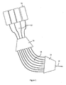
- Figure 1 shows an exemplary schematic view of a PIC comprising a plurality of electro-optical converters 11 (e.g. four discrete CWDM lasers) and an AWG multiplexer.
- the AWG multiplexer may comprise a plurality of waveguides 12, a first multimode section 13, a plurality of arrayed waveguides 16, a second multimode section 16 and an output waveguide 14.
- the electro-optical converters 11 are configured to convert electronic signals to optical signals, e.g. pulses of light at a specific wavelength.
- Light from the electro-optical converters 11 propagates through the first plurality of waveguides 12 and enters the first multimode section 13. From the first multimode section 13, the light enters the arrayed waveguides 16.
- the arrayed waveguides 16 are of different length so that an interference pattern is produced at the second multimode section 16.
- the plurality of waveguides 12, the first multimode section 13 and the plurality of arrayed waveguides 16 are arranged so that the produced interference pattern focuses the signals into the output waveguide 14 (e.g. a multimode waveguide).
- AWG based multiplexers may lead to low multiplexing losses.
- the AWG based multiplexers can be scaled for a higher number of channels, i.e. for a higher number of different CWDM wavelengths,
- this solution may be very costly as (i) the hybrid integration may require delicate alignment between passive and active waveguides and components; and as (ii) the monolithic integration may lead to large PIC-chip dimensions.
- MMI multimode interference
- a MMI multiplexer may be built as a PIC, where the light coming from a plurality of input fibers propagates through a multimode waveguide section into an output waveguide (e.g. an optical fiber).
- the basis of MMI multiplexers is the self-imaging principle of MMI. That is to say, by selecting the width and length of the multimode waveguide section, self-images of the different wavelengths can be coupled into the output waveguide.
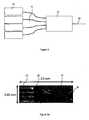
- FIGS 2 and 2a show schematic exemplary views of an MMI multiplexer in combination with a plurality of electro-optical converters 21 (e.g. four CWDM lasers).
- the MMI multiplexer may comprise a plurality of waveguides 22, a multimode section 23 and an output waveguide 24.
- the electro-optical converters 21 are configured to convert electronic signals to optical signals, e.g. pulses of light at specific wavelengths.
- the electro-optical converters 21 may be distributed feedback (DFB) lasers.
- the light from the electro-optical converters 21 propagates through the plurality of waveguides 22 and enters the multimode section 23.
- the plurality of waveguides 22 corresponds to a plurality of S-bend waveguides.
- Each mode in the multimode section 23 propagates with a different phase velocity and hence an interference pattern is produced that is dependent on the position along the multimode section 23.
- the electro-optical converters 21 are laterally positioned such that the curvature of each waveguide 22 does not exceed a predefined threshold in order to avoid signal losses.
- the curvature radius is preferably sufficiently large.
- the electro-optical converters 21 are laterally offset and the length of the S-bend waveguide 22 leading from a respective converter 21 to the multimode section 23 may be selected such that the losses due to the S-bends are kept below the predefined threshold.
- the PIC comprising four CWDM lasers and an MMI multiplexer to generate four optical channels as depicted in Figs. 2 and 2a may require around 2 mm 2 per device. That is to say, up to 3500 devices comprising the CWDM lasers and the MMI multiplexer may be manufactured from a 4 inch wafer.
- the multiplexing losses of the MMI multiplexer are at around 6 dB, which can be compensated with a booster.
- the size of the device will roughly have to be multiplied by 4 to maintain the same curvature radius of the S-bend waveguides 22.
- the MMI multiplexer losses may be greater than 9 dB, and the passive waveguides of the MMI multiplexer may be much longer. As a consequence, the fabrication yield and the multiplexing losses might become prohibitive when increasing the number of laterally placed DFB lasers (i.e. converters 21).
- FIG. 3 shows a schematic view of an MMI multiplexer using both parallel multiplexing as outlined in the context of Figs, 2 and 2a and serial multiplexing.
- the converters 21 are replaced by groups of converters 31aa, 31ab and 31ba, 31bb placed in series along the signal path.
- Fig. 3 illustrates two branches or groups of two converters 31aa, 31ab and 31ba, 31bb which are configured to generate light at different wavelengths.
- an MMI multiplexer may be used to multiplex the light coming from the plurality of electro-optical converters 31aa, 31ab, 31ba, 31bb.
- the MMI multiplexer preferably comprises a plurality of (S-bend) waveguides 32, a multimode section 33 and an output waveguide 34.
- the multimode section 33 may be arranged such that light from the plurality of waveguides 32 is multiplexed into the output waveguide 34, e.g, by using the self-imaging effect as described with reference to Figure 2 .
- the electro-optical converters 31aa, 31ab, 31ba, 31bb may be light emitting apparatuses.
- the light emitting apparatuses may be light emitting diodes (LED) or lasers.
- the lasers may be distributed feedback laser (DFB) lasers.
- the lasers may be directly modulated lasers (DML) or lasers using electro-absorption modulation (EAM), i.e. so called Electro-Absorption Modulated Lasers (EML).
- the material used for such converters 31aa, 31ab, 31ba, 31bb may be semiconductor material, such as Gallium arsenide, indium phosphide, gallium antimonide, and gallium nitride.
- Fig. 3 shows an arrangement where serial multiplexing of wavelengths is used in addition to parallel multiplexing based on MMI multiplexing.
- a given number of CWDM wavelengths can be multiplexed onto an output waveguide 34 using smaller MMI multiplexers which have tolerable multiplexing losses.
- the serial multiplexing is achieved by placing in series two or more electro-optical converters 31aa, 31ab.
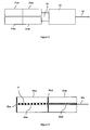
- the concept of serial multiplexing is outlined in the context of Fig. 4 which shows an embodiment of the converters 31aa, 31ab of Fig. 3 .
- the converters 31aa, 31ab comprise different active materials configured to convert an electrical signal into an optical signal. Furthermore, the converters 31aa and 31ab comprise an optical waveguide 37 for confining the emitted optical signal.
- the optical waveguide 37 traverses the two converters 31aa, 31ab. In particular, the waveguide 37 traverses a first active material of the first converter 31aa and a second active material of the second converter 31ab.
- light signals at the first wavelength and light signals at the second wavelength may be generated simultaneously within the waveguide 37, i.e. the light signals may be serially multiplexed onto the waveguide 37 of the converters 31aa, 31ab.
- Waveguide 37 may be connected to the waveguide 32a which corresponds to one of the waveguides 32 of the MMI multiplexer depicted In Fig. 3 .
- the waveguide 37 may be a single-mode waveguide, even for the short wavelengths carried by the waveguide 37.
- light emitted from the first and second active materials may be light of wavelengths in the wavelength interval of about 1450nm to about 1750 nm.
- parallel and serial multiplexing of the light generated by the electro-optical converters may be used, in order to design multi-wavelength CWDM emitters with a large numbers of optical channels, i.e. with a large number of CWDM wavelengths.
- this kind of serial multiplexing is feasible in the context of CWDM because of the large wavelength difference between different CWDM channels, which reduces the optical crosstalk between channels which are serially multiplexed.
- the second material used in the second converter 31ab is preferably selected such that light at the first wavelength passes through with low losses. Therefore, appropriate electro-optical materials for the first 31aa and the second 31ab converter may be selected. In an embodiment, the material of the first 31aa and second 31ab converter are selected such that the second wavelength is smaller than the first wavelength. In addition to designing the materials to emit a particular wavelength, the materials may be designed such that light at higher wavelengths than the particular emitted wavelength passes through the electro-optical material unaffected. As such, the second material of the second converter31ab may be designed to emit the second wavelength and it may be designed to not attenuate light at higher wavelengths than the second wavelength (e.g. light at the first wavelength).
- the material of the first converter 31aa may be selected such that light at the second wavelength, i.e. light at wavelengths which are lower than the first wavelength, is absorbed.
- electro-optical materials such as semiconductor materials comprising Indium (In), Gallium (Ga), Aluminium (AI), Arsenide (As) and/or Phosphorous (P).
- the first 31aa and second 31ab converter may comprise a first 36aa and a second 36ab grating, respectively, in order to provide DFB lasers.
- the first grating 36aa may have a grating period which allows for lasing at the first wavelength.
- the first 36aa and second 36ab gratings may be implemented as periodic variations of the refractive index of the material of the converter waveguide 37. The periodic variations of the refractive index are illustrated in Fig. 4 by a periodic succession of black and white sections of converter waveguide 37.
- the first 36aa and second 36ab gratings may have grating periods which allow for lasing at the first and second wavelength, respectively.
- the second grating 36ab may be transparent to the first wavelength.
- first 31aa and second 31ab converter may comprise a first 35aa and second 35ab rear reflector, respectively.
- the rear reflectors 35aa, 35ab may be configured to reflect the light emitted by the respective converter 31aa, 31ab, i.e. the light at the first and second wavelength, respectively.
- the second rear reflector 35ab i.e. the rear reflector of the second converter 31ab, may be configured to let pass (a high percentage, e.g. more than 50%, of) the light at the first wavelength.
- the light at the first and second wavelengths travels downstream towards the waveguide 32a. As such, the backward crosstalk between the different wavelengths can be reduced. Furthermore, the overall efficiency of the lasers can be improved.
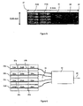
- FIG. 5 shows an example of a 4-to-1 MMI multiplexer and 4 pairs of serially multiplexed converters 31aa, 31ab.
- a multi-wavelength CWDM emitter using parallel and serial multiplexing is illustrated.
- 8 CWDM channels are multiplexed and the chip dimensions may be about 0.85*3 mm 2 .
- the dimensions were preferably about 0.85*2.5 mm 2 . That means that although the CWDM emitter according to Figure 5 multiplexes 8 channels, i.e.
- serial multiplexing does not substantially increase the multiplexing losses.
- the use of serial multiplexing may limit the increase in dimension and multiplexing losses compared to the increase in dimension (typically 400%) and the increase in multiplexing losses which are encountered when using only parallel multiplexing (e.g. when moving from a 4 channel MMI multiplexer to an 8 channel MMI multiplexer).
- the different wavelengths generated by the converters 31aa, 31ab may be arranged such that the wavelength difference between serially multiplexed wavelengths is high. This can be achieved by selecting four neighbouring wavelengths (1417nm, 1491nm, 1511nm, 1531nm) for parallel multiplexing and by serially multiplexing the following four wavelengths with the respective other wavelengths (1551nm, 1571nm, 1591nm, 1611nm). This is illustrated in Fig. 5 . By attributing the wavelengths to serial and parallel multiplexing in such a manner, the difference between wavelengths which are serially multiplexed can be maximized.
- the CWDM wavelengths are spaced by about 20 nm such that a large channel spacing of about 80 nm between adjacent serially multiplexed emitters can be achieved, thereby reducing the crosstalk.
- the material of the different converters is preferably selected appropriately.
- the material used for emitting light at about 1471 nm (resp. 1491nm, 1511nm and 1531nm), i.e. the material used for the second converter 31ab may be transparent to the light at about 1551 nm (resp. 1571nm, 1591nm and 1611nm), i.e. to the light emitted in the first converter 31aa. By doing this, the multiplexing losses caused by the serial multiplexing can be reduced. Furthermore, the material used for emitting light at about 1551 nm (resp. 1571nm, 1591nm and 1611nm), i.e.
- the material used for the first converter 31aa could completely absorb the emission at about 1471 nm (resp. 1491nm, 1511nm and 1531nm), i.e. the light emitted in the second converter 31ab. By doing this, the backward crosstalk could be reduced.
- a negatively biased section, or a reflector as outlined above may be introduced between the adjacent converters 31aa and 31ab in order to further reduce the backward crosstalk.
- T N comprises the lowest wavelengths
- T 1 comprises the highest wavelengths.
- Each active material M n may be configured to emit light at a wavelength ⁇ n belonging to the wavelength interval T n , respectively. It is assumed that material M N is positioned at the output end of the succession of converters C n and that material M 1 is positioned at the input or rear end, opposite or upstream to the output end, of the serially connected converters C n .
- material M N is positioned at the output end of waveguide W 37 and material M 1 is positioned at the rear end of waveguide W 37.
- Each active material M i is configured to leave unaffected light at a wavelength ⁇ j belonging to the wavelength interval T j , for j ⁇ i.
- each active material M i may be configured to absorb light at a wavelength ⁇ j belonging to the wavelength interval T j , for j>i.
- the light emitted by material M i passes through materials M i+1 ,...,M N , without being attenuated, in order to reach the output end of the waveguide W 37. Consequently, the serial multiplexing can be performed with low multiplexing losses.
- the light emitted by material M i which travels towards the rear end of the waveguide W 37 i.e. which travels towards materials M i-1 ,...,M 1 will be absorbed, thereby reducing backward crosstalk.
- the reflectors R n may be placed at the rear end of a converter C n .
- Each reflector R n may be configured to reflect wavelengths ⁇ n from the wavelengths interval T n .
- each reflector R n may be configured to let pass wavelengths ⁇ j from the wavelengths interval T j , for j ⁇ n.
- the same or other reflectors may be used for providing converters C n which comprise laser cavities.
- a serial connection of converters C n has been described in more general terms.
- a plurality of K such serial groups of converters may be placed in parallel, i.e. K such serial connections of converters may be placed in parallel onto a PIC, as shown e.g. in Fig.5 .
- the K output signals of the waveguides W k 37 may be optically multiplexed using parallel multiplexing, e.g. MMI multiplexing or AWG multiplexing.
- the serial multiplexing may be achieved by selecting appropriate active materials M kn .
- the wavelengths may be arranged within the matrix of converters C kn such that for some or all pairs of neighboring converters C ki , C kl+1 of a group of serial converters along waveguide W k , there are K-1 wavelengths ⁇ kn which are greater than wavelength ⁇ kl+1 emitted by converter C ki+1 and smaller than wavelength ⁇ kl emitted by converter C kj .
- this may be achieved by arranging the converter within the matrix such that ⁇ kn > ⁇ in , for k>i, and ⁇ kn > ⁇ ki , for i>n.
- Figure 6 shows an exemplary schematic view of an arrangement where three wavelengths are multiplexed in series in four groups 31a, 31b, 31c, 31d of converters prior to performing parallel multiplexing using a 4-to-1 MMI multiplexer.
- the MMI multiplexer may comprise a plurality of waveguides 32, a multimode section 33 and an output waveguide 34.
- the groups 31a, 31b, 31c, 31d of electro-optical converters comprise waveguides 37a, 37b, 37c, 37d which traverse the three converters 31aa-31ac, 31ba-31bc, 31ca-31cc and 31da-31dc, respectively.
- Each waveguide 37a, 37b, 37c, 37d traverses or passes through three different active materials, i.e. one active material per converter 31aa-31ac, 31ba-31bc, 31ca-31cc and 31da-31dc.
- each group 31a, 31b, 31c, 31d of converters emits three multiplexed CWDM wavelengths which are subsequently multiplexed using a 4-to-1 MMI multiplexer.
- a method and system of multiplexing light at different wavelengths has been described.
- a CWDM transmitter has been described which makes use of serial multiplexing of a plurality of wavelengths.
- serial multiplexing may be combined with parallel multiplexing (e.g. using MMI multiplexers or AWG multiplexers).
- parallel multiplexing e.g. using MMI multiplexers or AWG multiplexers.
- CWDM transmitters with a high degree of circuit integration may be provided.
- Such CWDM transmitters may be implemented as PICs for the use in optical access networks.
- any block diagrams herein represent conceptual views of illustrative circuitry embodying the principles of the invention.
- any flow charts, flow diagrams, state transition diagrams, pseudo code, and the like represent various processes which may be substantially represented in computer readable medium and so executed by a computer or processor, whether or not such computer or processor is explicitly shown.
Description
- The present document relates to a photonic integrated circuit (PIC) for multiplexing optical signals in a wavelength division multiplexing (WDM) system. In particular, the document relates to a method and system for reducing the size of a PIC for multiplexing optical signals in a WDM system.
- PICs have been developed to reduce packaging costs and the footprint of multi-wavelength emitters. One main market is the metropolitan area network.
- PICs are now foreseen for the access network. In the next generation of access networks, wavelength division multiplexing (WDM) will emerge to increase the flexibility of access networks, the number of subscribers and the optical budget (power splitters might be replaced by wavelength demultiplexers, which will also increase the number of possible subscribers).
- In fiber-optic communications, WDM is a technology which multiplexes multiple optical carrier signals on a single optical waveguide (e.g. an optical fiber) by using different wavelengths to carry different signals. This allows for a multiplication in capacity, in addition to enabling bidirectional communication over the same optical waveguide. In a WDM system, a multiplexer is used to merge the different optical signals corresponding to different wavelengths together onto the same waveguide, and a demultiplexer is typically used to isolate the different optical signals from the waveguide. When a device does both simultaneously, it can be used as an optical add-drop multiplexer.
-
US6201824 describes a two-dimensional matrix of complex coupled semiconductor DFB lasers. -
WO 96/37933 -
WO 03/032036 - The document "A robust WDM network laser source: the DFB cascade laser", by Sahlen et al., Conference on Optical Fiber Communications, Dallas, Feb. 16-21, 1997, pages 235-236, discloses a serially multiplexer DFB laser.
- In access networks, the cost of network components, e.g. the WDM transmitters, is an important issue. As a result, WDM will most likely be coarse (e.g. with a 20 nm wavelength spacing) in order to use uncooled optical emitters. Furthermore, in order to provide a WDM transmitter at low manufacturing cost, it is desirable to achieve a high degree of integration, i.e. it is desirable to provide a WDM transmitter which can transmit light at a high number of different wavelengths on the limited space of a PIC. The present document describes such a WDM transmitter and a corresponding method for implementing such a WDM transmitter.
- According to an aspect an optical transmitter or optical emitter is described. In particular, an optical CWDM emitter or transmitter is described. The emitter or transmitter may be integrated on a photonic integrated circuit (PIC). The transmitter may be configured to generate a plurality of optical signals at a corresponding plurality of different wavelengths multiplexed onto an output waveguide. The wavelengths may be in the 1300 nm to 1600 nm range. The spacing between the wavelengths may be about 20 nm or more.
- The transmitter may comprise a first and a second converter comprising different first and second active materials configured to emit light at a first and a different second wavelength. The first and second converters may be electro-optical converters configured to convert an electrical signal into an optical signal. In particular, the converter may be configured to convert a modulated electrical signal into a modulated optical signal.
- The transmitter may comprise a first converter waveguide traversing or passing through the first and second material of the first and second converter. The second material may be at an output end of the first converter waveguide and the first material may be at an input end (e.g. a rear end of the transmitter), upstream or opposite of the output end, of the first converter waveguide. The output end of the first converter waveguide may be directed towards the output end of the optical transmitter, i.e. towards the output waveguide. In other words, the output end of the first converter waveguide typically leads to the output waveguide.
- The second active material may be transparent to the light at the first wavelength. On the other hand, the first active material may be configured to absorb the light at the second wavelength. This may be achieved by selecting appropriate semiconducting materials, e.g. appropriate compositions of Indium (In), Gallium (Ga), Aluminium (AI), Arsenide (As) and/or Phosphorous (P). In particular, this may be achieved if the second wavelength is smaller than the first wavelength,
- The converters may be separated by a semitransparent reflector positioned at an output end of the first converter and at an input end of the second converter, the semitransparent reflector being substantially reflective two light at the second wavelength. By doing this, rearward crosstalk between the first and second wavelengths can be reduced. In addition, the semitransparent reflector may be transparent to light at the first wavelength.
- The first converter may comprise a first laser using the first active material and the second converter may comprise a second laser using the second active material. The lasers may be distributed feedback lasers (DFB). Such lasers may comprise a grating along the first converter waveguide. Such a grating may comprise a periodic variation of the refractive index of the material of the first converter waveguide, wherein the length of a periodic variation is typically referred to as a grating period or grating pitch Λ. In particular, the first converter may comprise a first grating at a first grating period, wherein the first grating period is selected based on to the first wavelength, i.e. the first grating period is associated with the first wavelength. In addition, the second converter may comprise a second grating at a second grating period, wherein the second grating period is selected based to the second wavelength, i.e. the second grating period is associated with the second wavelength. The first and second gratings, i.e. their effective refractive indexes neff and/or their grating periods, are typically configured to have a high reflectivity at the first and second wavelength, respectively. Furthermore, the first and second grating may be configured to be transparent at wavelengths other than the first and second wavelength, respectively.
- The transmitter may comprise K groups of N converters Ckn, k=1,...,K and n=1,...,N with K>1 and N>1. That is to say, in addition to the first and second converter which may be part of a first group of converters, the transmitter may comprise additional groups of converters. K may be greater or equal to 2, 4 and/or 8. K may be smaller or equal to 4, 8, 16 or 32. N may be greater or equal to 2, 3, 4, 8. N may be smaller or equal to 4, 8, 16 or 32. Each group of converters may be configured to generate N optical signals Skn at wavelengths λ kn, multiplexed onto a corresponding converter waveguide WK. As a result a serially multiplexed optical signal SK comprising N different wavelengths λkn, n=1,...,N, may be obtained at the output end of the converter waveguide WK. That is to say, in addition to the first converter waveguide the transmitter may comprise further converter waveguides Wk for the other additional groups of converters. The converters Ckn may comprise different active materials Mkn configured to emit light at the wavelength λkn, respectively. That is to say, each converter may comprise a different active material configured to emit light at a different wavelength.
- As already indicated above, the first and second converter may correspond to the converters C11 and C12, respectively. Furthermore, the first and second active materials may correspond to the materials M11 and M12, respectively. In addition, the first converter waveguide may correspond to the converter waveguide W1 traversing the first group of N optical converters C1n, n=1,...,N.
- In a similar manner to the first converter waveguide, the converter waveguides Wk, k=1,...,K, traverse the N active materials Mkn, n=1,...,N of the kth group of optical converters. In other words, each group of optical converters is traversed by a dedicated converter waveguide Wk. Without loss of generality, the indexing of the converters, wavelengths and materials is such that (for all k) material MkN is at an output end of the waveguide Wk and material Mk1 is at an input end, upstream and/or opposite of the output end, of the waveguide Wk.
- In order to perform the serial multiplexing along the kth group of converters, the material Mki may be configured to be transparent to and/or to leave unaffected light at a wavelength λkj with j<i. This condition may be met for all i,j=1,...,N. Alternatively or in addition, material Mkl may be configured to absorb light at a wavelength λkj with j>i. This condition may be met for all i,j=1,..,N. In other words, the different materials Mki may cause a selective absorption or passage of light, depending on the wavelength λkj of the light. Light at a wavelength λkj with j<i may pass the material Mki, while light at a wavelength λkj with j>i may be absorbed by material Mki.
- The transmitter may comprise an optical combiner configured to multiplex the K serially multiplexed optical signals Sk at the output end of the K converter waveguides Wk onto the output waveguide. This may be done using parallel multiplexing techniques, such as AWG (Arrayed Waveguide Grating) multiplexing or MMI (Multi-Mode Interference) multiplexing.
- The K groups of converters Ckn may be laterally spaced with respect to one another such that the output end of the K combiner waveguides Wk are at a lateral distance with respect to one another. In other words, the groups of converters may be placed in parallel with respect to their respective combiner waveguides Wk. I.e. the combiner waveguides Wk traversing the K groups of converters Ckn may be parallel. The combiner may comprise a first merging section, where the lateral distance between the K combiner waveguides Wk is progressively reduced. Furthermore, the combiner may comprise a second merging section, where the light at different wavelengths λkn carried in the combiner waveguides Wk, i.e. where the K serially multiplexed optical signals Sk, are superimposed within a joint waveguide leading to the output waveguide. The first merging section may comprise a plurality of S-bend waveguides configured to progressively reduce the distance between the K combiner waveguides Wk. Preferably, each combiner waveguide Wk is coupled to a corresponding S-bend waveguide.
- In order to reduce the crosstalk between wavelengths which are multiplexed onto a joint combiner waveguide Wk, the active materials Mkn and the corresponding wavelengths λkn may be arranged such that for some or all pairs of neighboring converters Cki, Cki+1 of the kth group of converters along the combiner waveguide Wk, there are K-1 wavelengths of the set of multiplexed wavelengths λkn, k=1,...,K and n=1,...,N, which are greater than wavelength λki+1 emitted by converter Cki+1 and smaller than wavelength λki emitted by converter Cki. In an embodiment, the active materials Mkn and the corresponding wavelengths λkn may be arranged such that λkn> λin, for any k>i, and λkn> λki, for any i>n.
- As outlined above, the converters Ckn, k=1,...,K and n=1,...,N may be lasers, in particular DF8 lasers. As such, the converters Ckn may comprise corresponding gratings Gkn, k=1,...,K and n=1,...,N at grating periods λkn, k=1,...,K and n=1,..,N, respectively. The gratings Gkn may be implemented as periodic variations of the refractive index of the converter waveguide Wk within the converter Ckn. That is to say, the grating Gkn may be implemented within the converter waveguide Wk, and the grating may be different for each converter traversed by the converter waveguide. Alternatively or in addition, the gratings Gkn may be implemented in a separate layer parallel to the converter waveguide Wk. A grating period λKn of the grating Gkn may be selected such that light at the wavelength λkn is reflected, i.e. the grating period Λkn of the grating Gkn may be associated with the wavelength λKn. Furthermore, the grating period λkn of the grating Gkn may be selected such that it is transparent to light at other wavelengths than wavelength λkn. In particular, the grating period Λkn of the grating Gkn may be selected such that it is transparent to light at wavelength λjn, for j<k. In an embodiment, the grating period Λkn is selected as

wherein neff is the effective index of the grating Gkn. That is to say, the grating period of a converter may be selected to be proportional to the wavelength emitted by the converter. - According to a further aspect, a method for generating a plurality of optical signals at a corresponding plurality of different wavelengths multiplexed onto an output waveguide is described, The method may comprise the step of providing a first and second converter comprising different first and second active materials configured to emit light at a first and a different second wavelength, In addition, the method may comprise the step of providing a first converter waveguide traversing the first and second material of the first and second converter, the second material being at an output end of the first converter waveguide and the first material being at an input end, upstream of the output end, of the first converter waveguide. The second active material may be transparent to the light at the first wavelength. The output end of the first converter waveguide may lead to the output waveguide.
- According to another aspect an optical network, e.g. an optical access network, comprising the optical transmitter or optical emitter described in the present document is described, The optical network may further comprise an optical transmission medium for transmitting the multiplexed optical signal. Furthermore, the optical network may comprise a corresponding optical receiver.
- Some embodiments of apparatus and methods in accordance with embodiments of the present invention are now described, by way of example only, and with reference to the accompanying drawings, in which:
-
Figure 1 shows a schematic view of an example of an AWG multiplexer and a plurality of electro-optical converters; -
Figures 2 and 2a show views of an example of a MMI multiplexer and a plurality of electro-optical converters; -
Figure 3 shows a schematic view of an example of a MMI multiplexer and a plurality of groups of electro-optical converters using serial multiplexing; -
Figure 4 shows a schematic view of an example of a group of electro-optical converters using serial multiplexing; -
Figure 5 shows an example of a MMI multiplexer and a plurality of groups of electro-optical converters using serial multiplexing; and -
Figure 6 shows a schematic view of another example of a MMI multiplexer and a plurality of groups of electro-optical converters using serial multiplexing. - integrated CWDM emitters which generate light at a plurality of wavelengths (e,g. four wavelengths) may be based on different concepts. The concepts may differ on the way that the light generated by a plurality of CWDM light sources is multiplexed onto a joint optical waveguide.
- A first option of multiplexing the light at different wavelength may use an Arrayed Waveguide Grating (AWG) based on silicon on insulator (SOI). An AWG multiplexer is usually built as a PIC, where the light coming from a multitude of input fibers, i.e. a multitude of optical channels, enters a first waveguide section, then propagates through several waveguides of different length and enters a second waveguide section, and is finally coupled into an output fiber. Wavelength multiplexing is based on an interference effect and the different optical path lengths of the waveguides; at least some frequency components of the input fibers propagate through the waveguides, and the output in the output fiber results from the superposition (interference) of these contributions of the at least some frequency components.
-
Figure 1 shows an exemplary schematic view of a PIC comprising a plurality of electro-optical converters 11 (e.g. four discrete CWDM lasers) and an AWG multiplexer. The AWG multiplexer may comprise a plurality ofwaveguides 12, a firstmultimode section 13, a plurality of arrayedwaveguides 16, a secondmultimode section 16 and anoutput waveguide 14. The electro-optical converters 11 are configured to convert electronic signals to optical signals, e.g. pulses of light at a specific wavelength. Light from the electro-optical converters 11 propagates through the first plurality ofwaveguides 12 and enters the firstmultimode section 13. From the firstmultimode section 13, the light enters the arrayedwaveguides 16. The arrayedwaveguides 16 are of different length so that an interference pattern is produced at the secondmultimode section 16. The plurality ofwaveguides 12, the firstmultimode section 13 and the plurality of arrayedwaveguides 16 are arranged so that the produced interference pattern focuses the signals into the output waveguide 14 (e.g. a multimode waveguide). - The use of AWG based multiplexers may lead to low multiplexing losses. The AWG based multiplexers can be scaled for a higher number of channels, i.e. for a higher number of different CWDM wavelengths, However, this solution may be very costly as (i) the hybrid integration may require delicate alignment between passive and active waveguides and components; and as (ii) the monolithic integration may lead to large PIC-chip dimensions.
- Another option for multiplexing light of a plurality of CWDM lasers is an integrated MMI (multimode interference) device or multiplexer. A MMI multiplexer may be built as a PIC, where the light coming from a plurality of input fibers propagates through a multimode waveguide section into an output waveguide (e.g. an optical fiber). The basis of MMI multiplexers is the self-imaging principle of MMI. That is to say, by selecting the width and length of the multimode waveguide section, self-images of the different wavelengths can be coupled into the output waveguide.
-
Figures 2 and 2a show schematic exemplary views of an MMI multiplexer in combination with a plurality of electro-optical converters 21 (e.g. four CWDM lasers). The MMI multiplexer may comprise a plurality ofwaveguides 22, amultimode section 23 and anoutput waveguide 24. The electro-optical converters 21 are configured to convert electronic signals to optical signals, e.g. pulses of light at specific wavelengths. The electro-optical converters 21 may be distributed feedback (DFB) lasers. The light from the electro-optical converters 21 propagates through the plurality ofwaveguides 22 and enters themultimode section 23. Typically, the plurality ofwaveguides 22 corresponds to a plurality of S-bend waveguides. Each mode in themultimode section 23 propagates with a different phase velocity and hence an interference pattern is produced that is dependent on the position along themultimode section 23. By selecting the width and length of themultimode section 23, and the configuration and position of theoutput waveguide 24 downstream of themultimode section 23, the different wavelengths provided by the plurality of electro-optical converters 21 can be multiplexed into theoutput waveguide 24. - Preferably, the electro-
optical converters 21 are laterally positioned such that the curvature of eachwaveguide 22 does not exceed a predefined threshold in order to avoid signal losses. In other words, the curvature radius is preferably sufficiently large. In other words, the electro-optical converters 21 are laterally offset and the length of the S-bend waveguide 22 leading from arespective converter 21 to themultimode section 23 may be selected such that the losses due to the S-bends are kept below the predefined threshold. - The PIC comprising four CWDM lasers and an MMI multiplexer to generate four optical channels as depicted in
Figs. 2 and 2a may require around 2 mm2 per device. That is to say, up to 3500 devices comprising the CWDM lasers and the MMI multiplexer may be manufactured from a 4 inch wafer. The multiplexing losses of the MMI multiplexer are at around 6 dB, which can be compensated with a booster. However, for 8 CWDM channels, i.e. when doubling the number of channels, the size of the device will roughly have to be multiplied by 4 to maintain the same curvature radius of the S-bend waveguides 22. This will reduce the number of PICs which can be manufactured from a 4 inch wafer to less than 1000, thus increasing the cost of the integrated CWDM transmitter, Moreover, the MMI multiplexer losses may be greater than 9 dB, and the passive waveguides of the MMI multiplexer may be much longer. As a consequence, the fabrication yield and the multiplexing losses might become prohibitive when increasing the number of laterally placed DFB lasers (i.e. converters 21). - The above mentioned multiplexing schemes which are based on AWG (
Fig. 1 ) and on MMI (Figs. 2, 2a ) will be referred to as parallel multiplexing, as the schemes are directed at multiplexing the light originating from a plurality of parallel (i.e. laterally spaced) electro-optical converters -
Figure 3 shows a schematic view of an MMI multiplexer using both parallel multiplexing as outlined in the context ofFigs, 2 and 2a and serial multiplexing. Theconverters 21 are replaced by groups of converters 31aa, 31ab and 31ba, 31bb placed in series along the signal path.Fig. 3 illustrates two branches or groups of two converters 31aa, 31ab and 31ba, 31bb which are configured to generate light at different wavelengths. As described with reference toFigure 2 , an MMI multiplexer may be used to multiplex the light coming from the plurality of electro-optical converters 31aa, 31ab, 31ba, 31bb. The MMI multiplexer preferably comprises a plurality of (S-bend)waveguides 32, amultimode section 33 and anoutput waveguide 34. Themultimode section 33 may be arranged such that light from the plurality ofwaveguides 32 is multiplexed into theoutput waveguide 34, e.g, by using the self-imaging effect as described with reference toFigure 2 . - The electro-optical converters 31aa, 31ab, 31ba, 31bb may be light emitting apparatuses. The light emitting apparatuses may be light emitting diodes (LED) or lasers. The lasers may be distributed feedback laser (DFB) lasers. In particular, the lasers may be directly modulated lasers (DML) or lasers using electro-absorption modulation (EAM), i.e. so called Electro-Absorption Modulated Lasers (EML). The material used for such converters 31aa, 31ab, 31ba, 31bb may be semiconductor material, such as Gallium arsenide, indium phosphide, gallium antimonide, and gallium nitride.
-
Fig. 3 shows an arrangement where serial multiplexing of wavelengths is used in addition to parallel multiplexing based on MMI multiplexing. As a result, a given number of CWDM wavelengths can be multiplexed onto anoutput waveguide 34 using smaller MMI multiplexers which have tolerable multiplexing losses. The serial multiplexing is achieved by placing in series two or more electro-optical converters 31aa, 31ab. The concept of serial multiplexing is outlined in the context ofFig. 4 which shows an embodiment of the converters 31aa, 31ab ofFig. 3 . - The converters 31aa, 31ab comprise different active materials configured to convert an electrical signal into an optical signal. Furthermore, the converters 31aa and 31ab comprise an
optical waveguide 37 for confining the emitted optical signal. Theoptical waveguide 37 traverses the two converters 31aa, 31ab. In particular, thewaveguide 37 traverses a first active material of the first converter 31aa and a second active material of the second converter 31ab. By electrically stimulating the first active material, light within a first wavelength interval (referred to as light at a first wavelength) may be emitted. By electrically stimulating the second active material light within a second wavelength interval (referred to as light at a second wavelength) may be emitted. By electrically stimulating both active materials, light signals at the first wavelength and light signals at the second wavelength may be generated simultaneously within thewaveguide 37, i.e. the light signals may be serially multiplexed onto thewaveguide 37 of the converters 31aa, 31ab.Waveguide 37 may be connected to thewaveguide 32a which corresponds to one of thewaveguides 32 of the MMI multiplexer depicted InFig. 3 . Thewaveguide 37 may be a single-mode waveguide, even for the short wavelengths carried by thewaveguide 37. In an embodiment, light emitted from the first and second active materials may be light of wavelengths in the wavelength interval of about 1450nm to about 1750 nm. By stimulating the active materials of converters 31aa, 31ab using a modulated electrical signal, modulated optical signals at a first and second wavelength, respectively, may be generated. - By the arrangement illustrated in
Figs. 3 and 4 , parallel and serial multiplexing of the light generated by the electro-optical converters, e.g. single-wavelengths CWDM emitters, may be used, in order to design multi-wavelength CWDM emitters with a large numbers of optical channels, i.e. with a large number of CWDM wavelengths. In particular, this kind of serial multiplexing is feasible in the context of CWDM because of the large wavelength difference between different CWDM channels, which reduces the optical crosstalk between channels which are serially multiplexed. - In view of the fact that the light at the first wavelength traverses the second converter 31ab, the second material used in the second converter 31ab is preferably selected such that light at the first wavelength passes through with low losses. Therefore, appropriate electro-optical materials for the first 31aa and the second 31ab converter may be selected. In an embodiment, the material of the first 31aa and second 31ab converter are selected such that the second wavelength is smaller than the first wavelength. In addition to designing the materials to emit a particular wavelength, the materials may be designed such that light at higher wavelengths than the particular emitted wavelength passes through the electro-optical material unaffected. As such, the second material of the second converter31ab may be designed to emit the second wavelength and it may be designed to not attenuate light at higher wavelengths than the second wavelength (e.g. light at the first wavelength).
- It should be noted that in addition to emitting light at the first wavelength, the material of the first converter 31aa may be selected such that light at the second wavelength, i.e. light at wavelengths which are lower than the first wavelength, is absorbed.
- The above conditions regarding the materials may be achieved by selecting appropriate compositions of electro-optical materials such as semiconductor materials comprising Indium (In), Gallium (Ga), Aluminium (AI), Arsenide (As) and/or Phosphorous (P).
- The first 31aa and second 31ab converter may comprise a first 36aa and a second 36ab grating, respectively, in order to provide DFB lasers. The first grating 36aa may have a grating period which allows for lasing at the first wavelength. The first 36aa and second 36ab gratings may be implemented as periodic variations of the refractive index of the material of the
converter waveguide 37. The periodic variations of the refractive index are illustrated inFig. 4 by a periodic succession of black and white sections ofconverter waveguide 37. The first 36aa and second 36ab gratings may have grating periods which allow for lasing at the first and second wavelength, respectively. Furthermore, the second grating 36ab may be transparent to the first wavelength. - In addition, the first 31aa and second 31ab converter may comprise a first 35aa and second 35ab rear reflector, respectively. The rear reflectors 35aa, 35ab may be configured to reflect the light emitted by the respective converter 31aa, 31ab, i.e. the light at the first and second wavelength, respectively. Furthermore, the second rear reflector 35ab, i.e. the rear reflector of the second converter 31ab, may be configured to let pass (a high percentage, e.g. more than 50%, of) the light at the first wavelength. The light at the first and second wavelengths travels downstream towards the
waveguide 32a. As such, the backward crosstalk between the different wavelengths can be reduced. Furthermore, the overall efficiency of the lasers can be improved. -
Figure 5 shows an example of a 4-to-1 MMI multiplexer and 4 pairs of serially multiplexed converters 31aa, 31ab. As such, a multi-wavelength CWDM emitter using parallel and serial multiplexing is illustrated. In the CWDM emitter according toFigure 5 , 8 CWDM channels are multiplexed and the chip dimensions may be about 0.85*3 mm2. In the CWDM emitter which uses only the 4-to-1 MMI multiplexer shown inFigure 2a , the dimensions were preferably about 0.85*2.5 mm2. That means that although the CWDM emitter according toFigure 5 multiplexes 8 channels, i.e. twice the number of channels that are multiplexed by the CWDM emitter shown inFigure 2 , the number of devices per wafer may only decrease by 20%. Furthermore, serial multiplexing does not substantially increase the multiplexing losses. As such, the use of serial multiplexing may limit the increase in dimension and multiplexing losses compared to the increase in dimension (typically 400%) and the increase in multiplexing losses which are encountered when using only parallel multiplexing (e.g. when moving from a 4 channel MMI multiplexer to an 8 channel MMI multiplexer). - The different wavelengths generated by the converters 31aa, 31ab may be arranged such that the wavelength difference between serially multiplexed wavelengths is high. This can be achieved by selecting four neighbouring wavelengths (1417nm, 1491nm, 1511nm, 1531nm) for parallel multiplexing and by serially multiplexing the following four wavelengths with the respective other wavelengths (1551nm, 1571nm, 1591nm, 1611nm). This is illustrated in
Fig. 5 . By attributing the wavelengths to serial and parallel multiplexing in such a manner, the difference between wavelengths which are serially multiplexed can be maximized. In the present example, the CWDM wavelengths are spaced by about 20 nm such that a large channel spacing of about 80 nm between adjacent serially multiplexed emitters can be achieved, thereby reducing the crosstalk. - As outlined above, the material of the different converters is preferably selected appropriately. The material used for emitting light at about 1471 nm (resp. 1491nm, 1511nm and 1531nm), i.e. the material used for the second converter 31ab, may be transparent to the light at about 1551 nm (resp. 1571nm, 1591nm and 1611nm), i.e. to the light emitted in the first converter 31aa. By doing this, the multiplexing losses caused by the serial multiplexing can be reduced. Furthermore, the material used for emitting light at about 1551 nm (resp. 1571nm, 1591nm and 1611nm), i.e. the material used for the first converter 31aa, could completely absorb the emission at about 1471 nm (resp. 1491nm, 1511nm and 1531nm), i.e. the light emitted in the second converter 31ab. By doing this, the backward crosstalk could be reduced. Alternatively or in addition, a negatively biased section, or a reflector as outlined above, may be introduced between the adjacent converters 31aa and 31ab in order to further reduce the backward crosstalk.
- It should be noted that while the two electro-optical converters 31aa, 31ab of
Figs. 4 and5 are illustrated for emitting and multiplexing light at two different wavelengths, the underlying principle of serial multiplexing may be extended to an arbitrary number of wavelengths, In general terms, awaveguide W 37 may traverse N serially concatenated converters Cn 31aa, 31ab emitting light at different wavelengths λn, n=1,..., N (N being an arbitrary integer value greater than one), Each wavelength λn belongs to a different wavelength interval Tn, n=1, ..., N. Without loss of generality, it is assumed that the different wavelength intervals Tn are ordered according to decreasing wavelengths, i.e. TN comprises the lowest wavelengths and T1 comprises the highest wavelengths. - In order to emit the different wavelengths λn, the succession of converters Cn 31aa, 31ab comprises different active materials Mn, n=1,..., N, i.e. the
waveguide W 37 traverses different active materials Mn. Each active material Mn may be configured to emit light at a wavelength λn belonging to the wavelength interval Tn, respectively. It is assumed that material MN is positioned at the output end of the succession of converters Cn and that material M1 is positioned at the input or rear end, opposite or upstream to the output end, of the serially connected converters Cn. In other words, material MN is positioned at the output end ofwaveguide W 37 and material M1 is positioned at the rear end ofwaveguide W 37. Each active material Mi is configured to leave unaffected light at a wavelength λj belonging to the wavelength interval Tj, for j<i. In addition, each active material Mi may be configured to absorb light at a wavelength λj belonging to the wavelength interval Tj, for j>i. As such, the light emitted by material Mi passes through materials Mi+1,...,MN, without being attenuated, in order to reach the output end of thewaveguide W 37. Consequently, the serial multiplexing can be performed with low multiplexing losses. On the other hand, the light emitted by material Mi which travels towards the rear end of thewaveguide W 37, i.e. which travels towards materials Mi-1,...,M1 will be absorbed, thereby reducing backward crosstalk. - Optionally, the different regions and materials may be separated by different reflectors Rn, n=1,..,N-1, or negatively biased sections, in order to further reduce the crosstalk. The reflectors Rn may be placed at the rear end of a converter Cn. Each reflector Rn may be configured to reflect wavelengths λn from the wavelengths interval Tn. Furthermore, each reflector Rn may be configured to let pass wavelengths λj from the wavelengths interval Tj, for j<n. The same or other reflectors may be used for providing converters Cn which comprise laser cavities.
- Above a serial connection of converters Cn has been described in more general terms. A plurality of K such serial groups of converters may be placed in parallel, i.e. K such serial connections of converters may be placed in parallel onto a PIC, as shown e.g. in
Fig.5 . As such, a matrix of converters Ckn with n=1,...,N and k=1,...,K, is obtained wherein the converters Ckn for a particular value k are connected in series using acommon waveguide W k 37 as outlined above. The K output signals of thewaveguides W k 37 may be optically multiplexed using parallel multiplexing, e.g. MMI multiplexing or AWG multiplexing. As such a CWDM transmitter or emitter configured to generate and multiplex K*N wavelengths λkn, with n=1,...,N and k=1,...,K may be provided. The CWDM transmitter comprises K groups of converters Ckn, wherein the kth group of converters provides N serially multiplexed optical signals at wavelengths λkn, n=1,...,N. As outlined above, the serial multiplexing may be achieved by selecting appropriate active materials Mkn. - In order to reduce the crosstalk between the serially multiplexed wavelengths λkn, the wavelengths may be arranged within the matrix of converters Ckn such that for some or all pairs of neighboring converters Cki, Ckl+1 of a group of serial converters along waveguide Wk, there are K-1 wavelengths λkn which are greater than wavelength λkl+1 emitted by converter Cki+1 and smaller than wavelength λkl emitted by converter Ckj. In an embodiment, this may be achieved by arranging the converter within the matrix such that λkn> λin, for k>i, and λkn> λki, for i>n.
-
Figure 6 shows an exemplary schematic view of an arrangement where three wavelengths are multiplexed in series in fourgroups Figs. 3 to 5 , the MMI multiplexer may comprise a plurality ofwaveguides 32, amultimode section 33 and anoutput waveguide 34. Thegroups waveguides waveguide group - In the present document a method and system of multiplexing light at different wavelengths has been described. In particular, a CWDM transmitter has been described which makes use of serial multiplexing of a plurality of wavelengths. In order to increase the distance between adjacent serially multiplexed wavelengths, and to thereby reduce the crosstalk, serial multiplexing may be combined with parallel multiplexing (e.g. using MMI multiplexers or AWG multiplexers). As a result, low cost and low loss CWDM transmitters may be provided. In particular, CWDM transmitters with a high degree of circuit integration may be provided. Such CWDM transmitters may be implemented as PICs for the use in optical access networks.
- It should be noted that the description and drawings merely illustrate the principles of the proposed methods and systems. It will thus be appreciated that those skilled in the art will be able to devise various arrangements that, although not explicitly described or shown herein, embody the principles of the invention and are included within its spirit and scope. Furthermore, all examples recited herein are principally intended expressly to be only for pedagogical purposes to aid the reader in understanding the principles of the proposed methods and systems and the concepts contributed by the inventors to furthering the art, and are to be construed as being without limitation to such specifically recited examples and conditions. Moreover, all statements herein reciting principles, aspects, and embodiments of the invention, as well as specific examples thereof, are intended to encompass equivalents thereof.
- Furthermore, it should be noted that any block diagrams herein represent conceptual views of illustrative circuitry embodying the principles of the invention. Similarly, it will be appreciated that any flow charts, flow diagrams, state transition diagrams, pseudo code, and the like represent various processes which may be substantially represented in computer readable medium and so executed by a computer or processor, whether or not such computer or processor is explicitly shown.
Claims (14)
- An optical transmitter configured to generate a plurality of optical signals at a corresponding plurality of different wavelengths multiplexed onto an output waveguide (34); the transmitter comprising:- a first (31aa) and second (31ab) converter comprising different first and second active materials configured to emit light at a first and a different second wavelength, respectively; wherein the first active material is configured to absorb the light at the second wavelength and wherein the second wavelength is smaller than the first wavelength; and- a first converter waveguide (37a) traversing the first and second material of the first (31aa) and second (31ab) converter, the second material being at an output end of the first converter waveguide (37a) and the first material being at an input end, upstream of the output end, of the first converter waveguide (37); wherein the second active material is transparent to the light at the first wavelength; and wherein the output end of the first converter waveguide (37a) is coupled to the output waveguide (34).
- The transmitter of any previous claim, wherein the first converter (31aa) comprises a first laser using the first active material and wherein the second converter (31ab) comprises a second laser using the second active material.
- The transmitter of any previous claim, wherein the first converter (31aa) comprises a first grating (36aa) at a first grating period associated with the first wavelength, and wherein the second converter (31ab) comprises a second grating (36ab) at a second grating period associated with the second wavelength.
- The transmitter of any previous claim, further comprising:- a semitransparent reflector (36ab) positioned at an output end of the first converter (31aa) and at an input end of the second converter (31ab), the semitransparent reflector (36ab) being substantially reflective to light at the second wavelength.
- The transmitter of any previous claim, wherein- the first and second material are semiconductor materials from a group of materials comprising Gallium, Indium, Aluminium, Phosphorous and/or Arsenide; and- the transmitter is a photonic integrated circuit.
- The transmitter of any previous claim, wherein the transmitter is an optical coarse wavelength division multiplexing transmitter.
- The transmitter of any previous claim, wherein- the transmitter comprises K groups (31a, 31b, 31c, 31d) of N converters Ckn, k=1,...,K and n=1,...,N with K>1 and N>1; each group configured to generate a serially multiplexed optical signal Sk comprising N optical signals at wavelengths λkn, n=1,...,N multiplexed onto a converter waveguide Wk;- the converters Ckn comprise different active materials Mkn configured to emit light at the wavelength Akn, respectively;- the first (31aa) and second (31ab) converter correspond to the converters C11 and C12, respectively;- the first and second active materials correspond to the materials M11 and M12, respectively;- the first converter waveguide (37a) corresponds to the converter waveguide W1 of the first group of N optical converters C1n;- the converter waveguides Wk, k=1,...,K, traverse the N active materials Mkn, n=1,...,N of the kth group of optical converters; material MkN being at an output end of the waveguide Wk and material Mk1 being at an input end, upstream of the output end, of the waveguide Wk;- material Mki is configured to be transparent to light at a wavelength λkj with j<i; and- material Mki is configured to absorb light at a wavelength λkj with j>i; and- the transmitter comprises an optical combiner (32, 33) configured to multiplex the K serially multiplexed optical signals Sk at the output end of the K converter waveguides Wk onto the output waveguide (34).
- The transmitter of claim 7, wherein- the converters Ckn comprise gratings Gkn at grating periods Λkn, respectively;- the first (36aa) and second (36ab) gratings correspond to the gratings G11 and G12, respectively; and- the grating periods Λkn are associated with the wavelengths λkn of the light emitted by the corresponding converters Ckn.
- The transmitter of any of claims 7 to 8, wherein- the K groups of converters Ckn are laterally spaced with respect to one another such that the output end of the K combiner waveguides Wk are at a lateral distance with respect to one another;- the combiner comprises a first merging section (32), where the lateral distance between the K combiner waveguides Wk is progressively reduced; and- the combiner comprises a second merging section (33), where the serially multiplexed optical signals Sk are superimposed within a joint waveguide leading to the output waveguide.
- The transmitter of claim 9, wherein the first merging section (32) comprises a plurality of S-bend waveguides configured to progressively reduce the distance between the K combiner waveguides Wk.
- The transmitter of any of claims 7 to 10, wherein the combiner (32, 33) is a multimode interference multiplexer.
- The transmitter of any of claims 7 to 11 wherein the active materials Mkn and the corresponding wavelengths λkn are arranged such that for at least one pair of neighboring converters Ckl, Ckl+1 of the kth group of converters along the combiner waveguide Wk, there are K-1 wavelengths of the set of wavelengths λkn, k=1,...,K and n=1,...,N, which are greater than wavelength λki+1 emitted by converter Cki+1 and smaller than wavelength λkl emitted by converter Cki.
- The transmitter of claim 12, wherein the active materials Mkn and the corresponding wavelengths λkn are arranged such that λkn> λln, for any k>i, and λkn> λki, for any i>n.
- A method for generating a plurality of optical signals at a corresponding plurality of different wavelengths multiplexed onto an output waveguide; the method comprising:- providing a first (31aa) and second (31ab) converter comprising different first and second active materials configured to emit light at a first and a different second wavelength; wherein the first active material is configured to absorb the light at the second wavelength and wherein the second wavelength is smaller than the first wavelength; and- providing a first converter waveguide (37a) traversing the first and second material of the first (31aa) and second (31ab) converter, the second material being at an output end of the first converter waveguide (37a) and the first material being at an input end, upstream of the output end, of the first converter waveguide (37a); wherein the second active material is transparent to the light at the first wavelength; and wherein the output end of the first converter waveguide (37a) is coupled to the output waveguide (34).
Priority Applications (8)
| Application Number | Priority Date | Filing Date | Title |
|---|---|---|---|
| EP10290509.8A EP2434594B1 (en) | 2010-09-27 | 2010-09-27 | Photonic integrated circuit for wavelength division multiplexing |
| PCT/EP2011/066586 WO2012041776A1 (en) | 2010-09-27 | 2011-09-23 | Photonic integrated circuit for wavelength division multiplexing |
| US13/824,736 US20140147129A1 (en) | 2010-09-27 | 2011-09-23 | Photonic integrated circuit for wavelength division multiplexing |
| SG2013021209A SG189049A1 (en) | 2010-09-27 | 2011-09-23 | Photonic integrated circuit for wavelength division multiplexing |
| KR1020137010602A KR20130058756A (en) | 2010-09-27 | 2011-09-23 | Photonic integrated circuit for wavelength division multiplexing |
| CN2011800466631A CN103125053A (en) | 2010-09-27 | 2011-09-23 | Photonic integrated circuit for wavelength division multiplexing |
| JP2013529661A JP2013542594A (en) | 2010-09-27 | 2011-09-23 | Photonic integrated circuit for wavelength division multiplexing |
| TW100134628A TWI472108B (en) | 2010-09-27 | 2011-09-26 | Photonic integrated circuit for wavelength division multiplexing |
Applications Claiming Priority (1)
| Application Number | Priority Date | Filing Date | Title |
|---|---|---|---|
| EP10290509.8A EP2434594B1 (en) | 2010-09-27 | 2010-09-27 | Photonic integrated circuit for wavelength division multiplexing |
Publications (2)
| Publication Number | Publication Date |
|---|---|
| EP2434594A1 EP2434594A1 (en) | 2012-03-28 |
| EP2434594B1 true EP2434594B1 (en) | 2014-05-14 |
Family
ID=43564924
Family Applications (1)
| Application Number | Title | Priority Date | Filing Date |
|---|---|---|---|
| EP10290509.8A Not-in-force EP2434594B1 (en) | 2010-09-27 | 2010-09-27 | Photonic integrated circuit for wavelength division multiplexing |
Country Status (8)
| Country | Link |
|---|---|
| US (1) | US20140147129A1 (en) |
| EP (1) | EP2434594B1 (en) |
| JP (1) | JP2013542594A (en) |
| KR (1) | KR20130058756A (en) |
| CN (1) | CN103125053A (en) |
| SG (1) | SG189049A1 (en) |
| TW (1) | TWI472108B (en) |
| WO (1) | WO2012041776A1 (en) |
Families Citing this family (4)
| Publication number | Priority date | Publication date | Assignee | Title |
|---|---|---|---|---|
| JP6407310B2 (en) * | 2015-08-18 | 2018-10-17 | 古河電気工業株式会社 | Optical semiconductor device |
| JP7124205B2 (en) | 2018-08-29 | 2022-08-23 | エーエスエムエル ホールディング エヌ.ブイ. | Compact alignment sensor arrangement |
| JP7326006B2 (en) * | 2019-04-12 | 2023-08-15 | 日本ルメンタム株式会社 | Optical semiconductor device, optical subassembly, and optical module |
| CN111830628B (en) * | 2020-07-24 | 2022-06-28 | 联合微电子中心有限责任公司 | Coarse wavelength division multiplexer/demultiplexer and optical communication equipment |
Family Cites Families (13)
| Publication number | Priority date | Publication date | Assignee | Title |
|---|---|---|---|---|
| JPS6027197B2 (en) * | 1977-08-04 | 1985-06-27 | 日本電気株式会社 | integrated light source |
| US4980892A (en) * | 1989-05-30 | 1990-12-25 | At&T Bell Laboratories | Optical system including wavelength-tunable semiconductor laser |
| US5031188A (en) * | 1990-04-30 | 1991-07-09 | At&T Bell Laboratories | Inline diplex lightwave transceiver |
| US5082343A (en) * | 1990-12-20 | 1992-01-21 | At&T Bell Laboratories | Isolated optical coupler |
| JP3149961B2 (en) * | 1991-01-30 | 2001-03-26 | キヤノン株式会社 | Multi-wavelength semiconductor laser device and driving method thereof |
| FR2734676B1 (en) * | 1995-05-23 | 1997-08-08 | Labeyrie Antoine | LASER EMISSION OR RECEPTION METHOD AND DEVICES FOR OPTICAL TRANSMISSION OF INFORMATION |
| JP2842387B2 (en) * | 1996-07-01 | 1999-01-06 | 日本電気株式会社 | Manufacturing method of semiconductor optical integrated device |
| US6104739A (en) * | 1997-12-24 | 2000-08-15 | Nortel Networks Corporation | Series of strongly complex coupled DFB lasers |
| JP2003014963A (en) * | 2001-06-27 | 2003-01-15 | Nec Corp | Semiconductor optical integrated element and its manufacturing method and module for optical communication |
| EP1488485B1 (en) * | 2001-10-09 | 2016-05-25 | Infinera Corporation | Transmitter photonic integrated circuit (txpic) chip with enhanced power and yield without on-chip amplification |
| JP2003179315A (en) * | 2001-12-12 | 2003-06-27 | Seiko Epson Corp | Optical module and optical communication system |
| JP2003195125A (en) * | 2001-12-27 | 2003-07-09 | Seiko Epson Corp | Optical module and optical communication system |
| US7376165B2 (en) * | 2004-01-30 | 2008-05-20 | Bayerische Motoren Werke Aktiengesellschaft | Laser diode alignment and packaging system for integrated optical and display subassemblies |
-
2010
- 2010-09-27 EP EP10290509.8A patent/EP2434594B1/en not_active Not-in-force
-
2011
- 2011-09-23 US US13/824,736 patent/US20140147129A1/en not_active Abandoned
- 2011-09-23 SG SG2013021209A patent/SG189049A1/en unknown
- 2011-09-23 WO PCT/EP2011/066586 patent/WO2012041776A1/en active Application Filing
- 2011-09-23 KR KR1020137010602A patent/KR20130058756A/en not_active Application Discontinuation
- 2011-09-23 JP JP2013529661A patent/JP2013542594A/en active Pending
- 2011-09-23 CN CN2011800466631A patent/CN103125053A/en active Pending
- 2011-09-26 TW TW100134628A patent/TWI472108B/en not_active IP Right Cessation
Also Published As
| Publication number | Publication date |
|---|---|
| JP2013542594A (en) | 2013-11-21 |
| US20140147129A1 (en) | 2014-05-29 |
| TW201232976A (en) | 2012-08-01 |
| CN103125053A (en) | 2013-05-29 |
| KR20130058756A (en) | 2013-06-04 |
| WO2012041776A1 (en) | 2012-04-05 |
| EP2434594A1 (en) | 2012-03-28 |
| TWI472108B (en) | 2015-02-01 |
| SG189049A1 (en) | 2013-05-31 |
Similar Documents
| Publication | Publication Date | Title |
|---|---|---|
| US7209609B2 (en) | Light source apparatus for WDM optical communication and optical communication system | |
| US20060193032A1 (en) | Multi-frequency light source | |
| JP7305556B2 (en) | integrated WDM optical transceiver | |
| EP2372936A1 (en) | Photonic integrated transmitter | |
| KR100678245B1 (en) | Passive optical network | |
| CN101501541A (en) | Method and system for grating taps for monitoring a dwdm transmitter array integrated on a plc platform | |
| EP2434594B1 (en) | Photonic integrated circuit for wavelength division multiplexing | |
| US20230353251A1 (en) | Photonic Integrated Circuit for High-Wavelength-Channel-Count Wavelength-Division-Multiplexed Systems | |
| US7031355B2 (en) | High efficiency single and multiple wavelength stabilized systems | |
| US7019907B2 (en) | Integrated lithium niobate based optical transmitter | |
| JP5871825B2 (en) | Wavelength multiplexing PON system | |
| JP4230934B2 (en) | Multi-channel optical modulator and multi-channel optical transmitter | |
| CN113411160B (en) | All-optical network based on Switchable Wavelength Connection (SWC) | |
| KR100611818B1 (en) | Transmission system and optical module for bi-directional communication in wavelength division multiplexing | |
| US20230246725A1 (en) | Wavelength-Division-Multiplexing Optical Circuit Implemented in Photonic Integrated Circuit for Optical Transmitter | |
| US20230291493A1 (en) | Wavelength-Multiplexed Optical Source with Reduced Temperature Sensitivity | |
| Ao et al. | A waveguide-based bidirectional optical delay unit with Bragg reflectors | |
| US20240007192A1 (en) | Photonic Integrated Circuit for High-Wavelength-Channel-Count Wavelength-Division-Multiplexed Systems | |
| EP1245997A1 (en) | Multi-frequency light source using four-wave mixing | |
| ES2751632T3 (en) | Multi-wavelength emitter tunable photonic integrated circuit | |
| WO2021100070A1 (en) | Optical modulator and optical transmitter | |
| CN114826403A (en) | Multi-path optical time delay system based on multi-core optical fiber | |
| JP3495665B2 (en) | Multi-wavelength batch converter | |
| Hoppe et al. | Enhanced Generalized Mach-Zehnder Interferometer for Tunable Channel Routing | |
| JP2004072690A (en) | Optical communication system |
Legal Events
| Date | Code | Title | Description |
|---|---|---|---|
| PUAI | Public reference made under article 153(3) epc to a published international application that has entered the european phase |
Free format text: ORIGINAL CODE: 0009012 |
|
| AK | Designated contracting states |
Kind code of ref document: A1 Designated state(s): AL AT BE BG CH CY CZ DE DK EE ES FI FR GB GR HR HU IE IS IT LI LT LU LV MC MK MT NL NO PL PT RO SE SI SK SM TR |
|
| AX | Request for extension of the european patent |
Extension state: BA ME RS |
|
| 17P | Request for examination filed |
Effective date: 20120928 |
|
| 17Q | First examination report despatched |
Effective date: 20121107 |
|
| 111Z | Information provided on other rights and legal means of execution |
Free format text: AL AT BE BG CH CY CZ DE DK EE ES FI FR GB GR HR HU IE IS IT LI LT LU LV MC MK MT NL NO PL PT RO SE SI SK SM TR Effective date: 20130410 |
|
| REG | Reference to a national code |
Ref country code: DE Ref legal event code: R079 Ref document number: 602010016061 Country of ref document: DE Free format text: PREVIOUS MAIN CLASS: H01S0005062500 Ipc: G02B0006120000 |
|
| RIC1 | Information provided on ipc code assigned before grant |
Ipc: G02B 6/12 20060101AFI20131011BHEP Ipc: H01S 5/026 20060101ALI20131011BHEP Ipc: H01S 5/0625 20060101ALI20131011BHEP Ipc: H01S 5/12 20060101ALI20131011BHEP Ipc: H01S 5/40 20060101ALI20131011BHEP |
|
| GRAP | Despatch of communication of intention to grant a patent |
Free format text: ORIGINAL CODE: EPIDOSNIGR1 |
|
| INTG | Intention to grant announced |
Effective date: 20131204 |
|
| RIN1 | Information on inventor provided before grant (corrected) |
Inventor name: BRENOT, ROMAIN Inventor name: GARREAU, ALEXANDRE |
|
| GRAS | Grant fee paid |
Free format text: ORIGINAL CODE: EPIDOSNIGR3 |
|
| GRAA | (expected) grant |
Free format text: ORIGINAL CODE: 0009210 |
|
| AK | Designated contracting states |
Kind code of ref document: B1 Designated state(s): AL AT BE BG CH CY CZ DE DK EE ES FI FR GB GR HR HU IE IS IT LI LT LU LV MC MK MT NL NO PL PT RO SE SI SK SM TR |
|
| REG | Reference to a national code |
Ref country code: GB Ref legal event code: FG4D |
|
| REG | Reference to a national code |
Ref country code: AT Ref legal event code: REF Ref document number: 668700 Country of ref document: AT Kind code of ref document: T Effective date: 20140615 |
|
| REG | Reference to a national code |
Ref country code: IE Ref legal event code: FG4D |
|
| REG | Reference to a national code |
Ref country code: DE Ref legal event code: R096 Ref document number: 602010016061 Country of ref document: DE Effective date: 20140626 |
|
| REG | Reference to a national code |
Ref country code: CH Ref legal event code: PCOW Free format text: NEW ADDRESS: 148/152 ROUTE DE LA REINE, 92100 BOULOGNE-BILLANCOURT (FR) |
|
| RAP2 | Party data changed (patent owner data changed or rights of a patent transferred) |
Owner name: ALCATEL LUCENT |
|
| REG | Reference to a national code |
Ref country code: AT Ref legal event code: MK05 Ref document number: 668700 Country of ref document: AT Kind code of ref document: T Effective date: 20140514 Ref country code: NL Ref legal event code: VDEP Effective date: 20140514 |
|
| REG | Reference to a national code |
Ref country code: LT Ref legal event code: MG4D |
|
| PG25 | Lapsed in a contracting state [announced via postgrant information from national office to epo] |
Ref country code: IS Free format text: LAPSE BECAUSE OF FAILURE TO SUBMIT A TRANSLATION OF THE DESCRIPTION OR TO PAY THE FEE WITHIN THE PRESCRIBED TIME-LIMIT Effective date: 20140914 Ref country code: GR Free format text: LAPSE BECAUSE OF FAILURE TO SUBMIT A TRANSLATION OF THE DESCRIPTION OR TO PAY THE FEE WITHIN THE PRESCRIBED TIME-LIMIT Effective date: 20140815 Ref country code: LT Free format text: LAPSE BECAUSE OF FAILURE TO SUBMIT A TRANSLATION OF THE DESCRIPTION OR TO PAY THE FEE WITHIN THE PRESCRIBED TIME-LIMIT Effective date: 20140514 Ref country code: FI Free format text: LAPSE BECAUSE OF FAILURE TO SUBMIT A TRANSLATION OF THE DESCRIPTION OR TO PAY THE FEE WITHIN THE PRESCRIBED TIME-LIMIT Effective date: 20140514 Ref country code: CY Free format text: LAPSE BECAUSE OF FAILURE TO SUBMIT A TRANSLATION OF THE DESCRIPTION OR TO PAY THE FEE WITHIN THE PRESCRIBED TIME-LIMIT Effective date: 20140514 Ref country code: NO Free format text: LAPSE BECAUSE OF FAILURE TO SUBMIT A TRANSLATION OF THE DESCRIPTION OR TO PAY THE FEE WITHIN THE PRESCRIBED TIME-LIMIT Effective date: 20140814 |
|
| PGFP | Annual fee paid to national office [announced via postgrant information from national office to epo] |
Ref country code: DE Payment date: 20140922 Year of fee payment: 5 |
|
| PG25 | Lapsed in a contracting state [announced via postgrant information from national office to epo] |
Ref country code: LV Free format text: LAPSE BECAUSE OF FAILURE TO SUBMIT A TRANSLATION OF THE DESCRIPTION OR TO PAY THE FEE WITHIN THE PRESCRIBED TIME-LIMIT Effective date: 20140514 Ref country code: SE Free format text: LAPSE BECAUSE OF FAILURE TO SUBMIT A TRANSLATION OF THE DESCRIPTION OR TO PAY THE FEE WITHIN THE PRESCRIBED TIME-LIMIT Effective date: 20140514 Ref country code: HR Free format text: LAPSE BECAUSE OF FAILURE TO SUBMIT A TRANSLATION OF THE DESCRIPTION OR TO PAY THE FEE WITHIN THE PRESCRIBED TIME-LIMIT Effective date: 20140514 Ref country code: ES Free format text: LAPSE BECAUSE OF FAILURE TO SUBMIT A TRANSLATION OF THE DESCRIPTION OR TO PAY THE FEE WITHIN THE PRESCRIBED TIME-LIMIT Effective date: 20140514 Ref country code: PL Free format text: LAPSE BECAUSE OF FAILURE TO SUBMIT A TRANSLATION OF THE DESCRIPTION OR TO PAY THE FEE WITHIN THE PRESCRIBED TIME-LIMIT Effective date: 20140514 Ref country code: AT Free format text: LAPSE BECAUSE OF FAILURE TO SUBMIT A TRANSLATION OF THE DESCRIPTION OR TO PAY THE FEE WITHIN THE PRESCRIBED TIME-LIMIT Effective date: 20140514 |
|
| PGFP | Annual fee paid to national office [announced via postgrant information from national office to epo] |
Ref country code: FR Payment date: 20140919 Year of fee payment: 5 Ref country code: GB Payment date: 20140919 Year of fee payment: 5 |
|
| PG25 | Lapsed in a contracting state [announced via postgrant information from national office to epo] |
Ref country code: PT Free format text: LAPSE BECAUSE OF FAILURE TO SUBMIT A TRANSLATION OF THE DESCRIPTION OR TO PAY THE FEE WITHIN THE PRESCRIBED TIME-LIMIT Effective date: 20140915 |
|
| PG25 | Lapsed in a contracting state [announced via postgrant information from national office to epo] |
Ref country code: DK Free format text: LAPSE BECAUSE OF FAILURE TO SUBMIT A TRANSLATION OF THE DESCRIPTION OR TO PAY THE FEE WITHIN THE PRESCRIBED TIME-LIMIT Effective date: 20140514 Ref country code: EE Free format text: LAPSE BECAUSE OF FAILURE TO SUBMIT A TRANSLATION OF THE DESCRIPTION OR TO PAY THE FEE WITHIN THE PRESCRIBED TIME-LIMIT Effective date: 20140514 Ref country code: BE Free format text: LAPSE BECAUSE OF FAILURE TO SUBMIT A TRANSLATION OF THE DESCRIPTION OR TO PAY THE FEE WITHIN THE PRESCRIBED TIME-LIMIT Effective date: 20140514 Ref country code: SK Free format text: LAPSE BECAUSE OF FAILURE TO SUBMIT A TRANSLATION OF THE DESCRIPTION OR TO PAY THE FEE WITHIN THE PRESCRIBED TIME-LIMIT Effective date: 20140514 Ref country code: RO Free format text: LAPSE BECAUSE OF FAILURE TO SUBMIT A TRANSLATION OF THE DESCRIPTION OR TO PAY THE FEE WITHIN THE PRESCRIBED TIME-LIMIT Effective date: 20140514 Ref country code: CZ Free format text: LAPSE BECAUSE OF FAILURE TO SUBMIT A TRANSLATION OF THE DESCRIPTION OR TO PAY THE FEE WITHIN THE PRESCRIBED TIME-LIMIT Effective date: 20140514 |
|
| REG | Reference to a national code |
Ref country code: DE Ref legal event code: R097 Ref document number: 602010016061 Country of ref document: DE |
|
| PG25 | Lapsed in a contracting state [announced via postgrant information from national office to epo] |
Ref country code: NL Free format text: LAPSE BECAUSE OF FAILURE TO SUBMIT A TRANSLATION OF THE DESCRIPTION OR TO PAY THE FEE WITHIN THE PRESCRIBED TIME-LIMIT Effective date: 20140514 |
|
| PLBE | No opposition filed within time limit |
Free format text: ORIGINAL CODE: 0009261 |
|
| STAA | Information on the status of an ep patent application or granted ep patent |
Free format text: STATUS: NO OPPOSITION FILED WITHIN TIME LIMIT |
|
| 26N | No opposition filed |
Effective date: 20150217 |
|
| PG25 | Lapsed in a contracting state [announced via postgrant information from national office to epo] |
Ref country code: LU Free format text: LAPSE BECAUSE OF FAILURE TO SUBMIT A TRANSLATION OF THE DESCRIPTION OR TO PAY THE FEE WITHIN THE PRESCRIBED TIME-LIMIT Effective date: 20140927 Ref country code: IT Free format text: LAPSE BECAUSE OF FAILURE TO SUBMIT A TRANSLATION OF THE DESCRIPTION OR TO PAY THE FEE WITHIN THE PRESCRIBED TIME-LIMIT Effective date: 20140514 Ref country code: MC Free format text: LAPSE BECAUSE OF FAILURE TO SUBMIT A TRANSLATION OF THE DESCRIPTION OR TO PAY THE FEE WITHIN THE PRESCRIBED TIME-LIMIT Effective date: 20140514 |
|
| REG | Reference to a national code |
Ref country code: CH Ref legal event code: PL |
|
| REG | Reference to a national code |
Ref country code: DE Ref legal event code: R097 Ref document number: 602010016061 Country of ref document: DE Effective date: 20150217 |
|
| REG | Reference to a national code |
Ref country code: IE Ref legal event code: MM4A |
|
| PG25 | Lapsed in a contracting state [announced via postgrant information from national office to epo] |
Ref country code: CH Free format text: LAPSE BECAUSE OF NON-PAYMENT OF DUE FEES Effective date: 20140930 Ref country code: LI Free format text: LAPSE BECAUSE OF NON-PAYMENT OF DUE FEES Effective date: 20140930 Ref country code: SI Free format text: LAPSE BECAUSE OF FAILURE TO SUBMIT A TRANSLATION OF THE DESCRIPTION OR TO PAY THE FEE WITHIN THE PRESCRIBED TIME-LIMIT Effective date: 20140514 |
|
| PG25 | Lapsed in a contracting state [announced via postgrant information from national office to epo] |
Ref country code: IE Free format text: LAPSE BECAUSE OF NON-PAYMENT OF DUE FEES Effective date: 20140927 |
|
| REG | Reference to a national code |
Ref country code: DE Ref legal event code: R119 Ref document number: 602010016061 Country of ref document: DE |
|
| PG25 | Lapsed in a contracting state [announced via postgrant information from national office to epo] |
Ref country code: SM Free format text: LAPSE BECAUSE OF FAILURE TO SUBMIT A TRANSLATION OF THE DESCRIPTION OR TO PAY THE FEE WITHIN THE PRESCRIBED TIME-LIMIT Effective date: 20140514 |
|
| GBPC | Gb: european patent ceased through non-payment of renewal fee |
Effective date: 20150927 |
|
| PG25 | Lapsed in a contracting state [announced via postgrant information from national office to epo] |
Ref country code: MT Free format text: LAPSE BECAUSE OF FAILURE TO SUBMIT A TRANSLATION OF THE DESCRIPTION OR TO PAY THE FEE WITHIN THE PRESCRIBED TIME-LIMIT Effective date: 20140514 Ref country code: BG Free format text: LAPSE BECAUSE OF FAILURE TO SUBMIT A TRANSLATION OF THE DESCRIPTION OR TO PAY THE FEE WITHIN THE PRESCRIBED TIME-LIMIT Effective date: 20140514 |
|
| REG | Reference to a national code |
Ref country code: FR Ref legal event code: ST Effective date: 20160531 |
|
| PG25 | Lapsed in a contracting state [announced via postgrant information from national office to epo] |
Ref country code: HU Free format text: LAPSE BECAUSE OF FAILURE TO SUBMIT A TRANSLATION OF THE DESCRIPTION OR TO PAY THE FEE WITHIN THE PRESCRIBED TIME-LIMIT; INVALID AB INITIO Effective date: 20100927 Ref country code: TR Free format text: LAPSE BECAUSE OF FAILURE TO SUBMIT A TRANSLATION OF THE DESCRIPTION OR TO PAY THE FEE WITHIN THE PRESCRIBED TIME-LIMIT Effective date: 20140514 Ref country code: DE Free format text: LAPSE BECAUSE OF NON-PAYMENT OF DUE FEES Effective date: 20160401 Ref country code: GB Free format text: LAPSE BECAUSE OF NON-PAYMENT OF DUE FEES Effective date: 20150927 |
|
| PG25 | Lapsed in a contracting state [announced via postgrant information from national office to epo] |
Ref country code: FR Free format text: LAPSE BECAUSE OF NON-PAYMENT OF DUE FEES Effective date: 20150930 |
|
| PG25 | Lapsed in a contracting state [announced via postgrant information from national office to epo] |
Ref country code: MK Free format text: LAPSE BECAUSE OF FAILURE TO SUBMIT A TRANSLATION OF THE DESCRIPTION OR TO PAY THE FEE WITHIN THE PRESCRIBED TIME-LIMIT Effective date: 20140514 |
|
| PG25 | Lapsed in a contracting state [announced via postgrant information from national office to epo] |
Ref country code: AL Free format text: LAPSE BECAUSE OF FAILURE TO SUBMIT A TRANSLATION OF THE DESCRIPTION OR TO PAY THE FEE WITHIN THE PRESCRIBED TIME-LIMIT Effective date: 20140514 |