EP2434594B1 - Photonische integrierte Schaltung für Wellenlängenmultiplex-Verfahren - Google Patents
Photonische integrierte Schaltung für Wellenlängenmultiplex-Verfahren Download PDFInfo
- Publication number
- EP2434594B1 EP2434594B1 EP10290509.8A EP10290509A EP2434594B1 EP 2434594 B1 EP2434594 B1 EP 2434594B1 EP 10290509 A EP10290509 A EP 10290509A EP 2434594 B1 EP2434594 B1 EP 2434594B1
- Authority
- EP
- European Patent Office
- Prior art keywords
- converter
- waveguide
- wavelength
- transmitter
- converters
- Prior art date
- Legal status (The legal status is an assumption and is not a legal conclusion. Google has not performed a legal analysis and makes no representation as to the accuracy of the status listed.)
- Not-in-force
Links
- 230000003287 optical effect Effects 0.000 claims description 61
- 239000000463 material Substances 0.000 claims description 58
- 239000011149 active material Substances 0.000 claims description 42
- 238000000034 method Methods 0.000 claims description 13
- 238000011144 upstream manufacturing Methods 0.000 claims description 7
- 229910052782 aluminium Inorganic materials 0.000 claims description 5
- XAGFODPZIPBFFR-UHFFFAOYSA-N aluminium Chemical compound [Al] XAGFODPZIPBFFR-UHFFFAOYSA-N 0.000 claims description 5
- 239000004411 aluminium Substances 0.000 claims description 5
- 239000004065 semiconductor Substances 0.000 claims description 5
- GYHNNYVSQQEPJS-UHFFFAOYSA-N Gallium Chemical compound [Ga] GYHNNYVSQQEPJS-UHFFFAOYSA-N 0.000 claims description 3
- 229910052733 gallium Inorganic materials 0.000 claims description 3
- BHEPBYXIRTUNPN-UHFFFAOYSA-N hydridophosphorus(.) (triplet) Chemical compound [PH] BHEPBYXIRTUNPN-UHFFFAOYSA-N 0.000 claims description 3
- 229910052738 indium Inorganic materials 0.000 claims description 3
- APFVFJFRJDLVQX-UHFFFAOYSA-N indium atom Chemical compound [In] APFVFJFRJDLVQX-UHFFFAOYSA-N 0.000 claims description 3
- 230000000737 periodic effect Effects 0.000 description 6
- 208000036758 Postinfectious cerebellitis Diseases 0.000 description 5
- 239000000835 fiber Substances 0.000 description 5
- 230000010354 integration Effects 0.000 description 5
- 239000011159 matrix material Substances 0.000 description 4
- 230000004936 stimulating effect Effects 0.000 description 4
- 238000010521 absorption reaction Methods 0.000 description 3
- 238000010586 diagram Methods 0.000 description 3
- 239000013307 optical fiber Substances 0.000 description 3
- 230000006854 communication Effects 0.000 description 2
- 238000004891 communication Methods 0.000 description 2
- 230000000694 effects Effects 0.000 description 2
- 238000003384 imaging method Methods 0.000 description 2
- 238000004519 manufacturing process Methods 0.000 description 2
- 239000000203 mixture Substances 0.000 description 2
- JBRZTFJDHDCESZ-UHFFFAOYSA-N AsGa Chemical compound [As]#[Ga] JBRZTFJDHDCESZ-UHFFFAOYSA-N 0.000 description 1
- 229910002601 GaN Inorganic materials 0.000 description 1
- 229910001218 Gallium arsenide Inorganic materials 0.000 description 1
- JMASRVWKEDWRBT-UHFFFAOYSA-N Gallium nitride Chemical compound [Ga]#N JMASRVWKEDWRBT-UHFFFAOYSA-N 0.000 description 1
- GPXJNWSHGFTCBW-UHFFFAOYSA-N Indium phosphide Chemical compound [In]#P GPXJNWSHGFTCBW-UHFFFAOYSA-N 0.000 description 1
- 230000002238 attenuated effect Effects 0.000 description 1
- 230000007175 bidirectional communication Effects 0.000 description 1
- 230000005540 biological transmission Effects 0.000 description 1
- 230000003247 decreasing effect Effects 0.000 description 1
- 230000001419 dependent effect Effects 0.000 description 1
- 238000005516 engineering process Methods 0.000 description 1
- VTGARNNDLOTBET-UHFFFAOYSA-N gallium antimonide Chemical compound [Sb]#[Ga] VTGARNNDLOTBET-UHFFFAOYSA-N 0.000 description 1
- 239000012212 insulator Substances 0.000 description 1
- 238000004806 packaging method and process Methods 0.000 description 1
- 230000000135 prohibitive effect Effects 0.000 description 1
- 238000002310 reflectometry Methods 0.000 description 1
- 229910052710 silicon Inorganic materials 0.000 description 1
- 239000010703 silicon Substances 0.000 description 1
- 230000007704 transition Effects 0.000 description 1
Images
Classifications
-
- H—ELECTRICITY
- H04—ELECTRIC COMMUNICATION TECHNIQUE
- H04B—TRANSMISSION
- H04B10/00—Transmission systems employing electromagnetic waves other than radio-waves, e.g. infrared, visible or ultraviolet light, or employing corpuscular radiation, e.g. quantum communication
- H04B10/50—Transmitters
- H04B10/572—Wavelength control
-
- G—PHYSICS
- G02—OPTICS
- G02B—OPTICAL ELEMENTS, SYSTEMS OR APPARATUS
- G02B6/00—Light guides; Structural details of arrangements comprising light guides and other optical elements, e.g. couplings
- G02B6/10—Light guides; Structural details of arrangements comprising light guides and other optical elements, e.g. couplings of the optical waveguide type
- G02B6/12—Light guides; Structural details of arrangements comprising light guides and other optical elements, e.g. couplings of the optical waveguide type of the integrated circuit kind
- G02B6/12007—Light guides; Structural details of arrangements comprising light guides and other optical elements, e.g. couplings of the optical waveguide type of the integrated circuit kind forming wavelength selective elements, e.g. multiplexer, demultiplexer
- G02B6/12009—Light guides; Structural details of arrangements comprising light guides and other optical elements, e.g. couplings of the optical waveguide type of the integrated circuit kind forming wavelength selective elements, e.g. multiplexer, demultiplexer comprising arrayed waveguide grating [AWG] devices, i.e. with a phased array of waveguides
-
- H—ELECTRICITY
- H01—ELECTRIC ELEMENTS
- H01S—DEVICES USING THE PROCESS OF LIGHT AMPLIFICATION BY STIMULATED EMISSION OF RADIATION [LASER] TO AMPLIFY OR GENERATE LIGHT; DEVICES USING STIMULATED EMISSION OF ELECTROMAGNETIC RADIATION IN WAVE RANGES OTHER THAN OPTICAL
- H01S5/00—Semiconductor lasers
- H01S5/02—Structural details or components not essential to laser action
- H01S5/026—Monolithically integrated components, e.g. waveguides, monitoring photo-detectors, drivers
- H01S5/0265—Intensity modulators
-
- H—ELECTRICITY
- H01—ELECTRIC ELEMENTS
- H01S—DEVICES USING THE PROCESS OF LIGHT AMPLIFICATION BY STIMULATED EMISSION OF RADIATION [LASER] TO AMPLIFY OR GENERATE LIGHT; DEVICES USING STIMULATED EMISSION OF ELECTROMAGNETIC RADIATION IN WAVE RANGES OTHER THAN OPTICAL
- H01S5/00—Semiconductor lasers
- H01S5/02—Structural details or components not essential to laser action
- H01S5/026—Monolithically integrated components, e.g. waveguides, monitoring photo-detectors, drivers
- H01S5/0268—Integrated waveguide grating router, e.g. emission of a multi-wavelength laser array is combined by a "dragon router"
-
- H—ELECTRICITY
- H01—ELECTRIC ELEMENTS
- H01S—DEVICES USING THE PROCESS OF LIGHT AMPLIFICATION BY STIMULATED EMISSION OF RADIATION [LASER] TO AMPLIFY OR GENERATE LIGHT; DEVICES USING STIMULATED EMISSION OF ELECTROMAGNETIC RADIATION IN WAVE RANGES OTHER THAN OPTICAL
- H01S5/00—Semiconductor lasers
- H01S5/10—Construction or shape of the optical resonator, e.g. extended or external cavity, coupled cavities, bent-guide, varying width, thickness or composition of the active region
- H01S5/12—Construction or shape of the optical resonator, e.g. extended or external cavity, coupled cavities, bent-guide, varying width, thickness or composition of the active region the resonator having a periodic structure, e.g. in distributed feedback [DFB] lasers
-
- H—ELECTRICITY
- H01—ELECTRIC ELEMENTS
- H01S—DEVICES USING THE PROCESS OF LIGHT AMPLIFICATION BY STIMULATED EMISSION OF RADIATION [LASER] TO AMPLIFY OR GENERATE LIGHT; DEVICES USING STIMULATED EMISSION OF ELECTROMAGNETIC RADIATION IN WAVE RANGES OTHER THAN OPTICAL
- H01S5/00—Semiconductor lasers
- H01S5/40—Arrangement of two or more semiconductor lasers, not provided for in groups H01S5/02 - H01S5/30
- H01S5/4025—Array arrangements, e.g. constituted by discrete laser diodes or laser bar
- H01S5/4031—Edge-emitting structures
-
- H—ELECTRICITY
- H01—ELECTRIC ELEMENTS
- H01S—DEVICES USING THE PROCESS OF LIGHT AMPLIFICATION BY STIMULATED EMISSION OF RADIATION [LASER] TO AMPLIFY OR GENERATE LIGHT; DEVICES USING STIMULATED EMISSION OF ELECTROMAGNETIC RADIATION IN WAVE RANGES OTHER THAN OPTICAL
- H01S5/00—Semiconductor lasers
- H01S5/40—Arrangement of two or more semiconductor lasers, not provided for in groups H01S5/02 - H01S5/30
- H01S5/4025—Array arrangements, e.g. constituted by discrete laser diodes or laser bar
- H01S5/4087—Array arrangements, e.g. constituted by discrete laser diodes or laser bar emitting more than one wavelength
-
- H—ELECTRICITY
- H04—ELECTRIC COMMUNICATION TECHNIQUE
- H04J—MULTIPLEX COMMUNICATION
- H04J14/00—Optical multiplex systems
- H04J14/02—Wavelength-division multiplex systems
- H04J14/03—WDM arrangements
- H04J14/0307—Multiplexers; Demultiplexers
Definitions
- the present document relates to a photonic integrated circuit (PIC) for multiplexing optical signals in a wavelength division multiplexing (WDM) system.
- PIC photonic integrated circuit
- WDM wavelength division multiplexing
- the document relates to a method and system for reducing the size of a PIC for multiplexing optical signals in a WDM system.
- PICs have been developed to reduce packaging costs and the footprint of multi-wavelength emitters.
- One main market is the metropolitan area network.
- wavelength division multiplexing will emerge to increase the flexibility of access networks, the number of subscribers and the optical budget (power splitters might be replaced by wavelength demultiplexers, which will also increase the number of possible subscribers).
- WDM is a technology which multiplexes multiple optical carrier signals on a single optical waveguide (e.g. an optical fiber) by using different wavelengths to carry different signals. This allows for a multiplication in capacity, in addition to enabling bidirectional communication over the same optical waveguide.
- a multiplexer is used to merge the different optical signals corresponding to different wavelengths together onto the same waveguide, and a demultiplexer is typically used to isolate the different optical signals from the waveguide. When a device does both simultaneously, it can be used as an optical add-drop multiplexer.
- US6201824 describes a two-dimensional matrix of complex coupled semiconductor DFB lasers.
- WO 96/37933 discloses a serially multiplexed laser wherein different electrodes apply different signals on an electro-optical waveguide.
- WO 03/032036 discloses a serially multiplexed laser comprising DFB sources.
- the cost of network components e.g. the WDM transmitters
- WDM will most likely be coarse (e.g. with a 20 nm wavelength spacing) in order to use uncooled optical emitters.
- it is desirable to achieve a high degree of integration i.e. it is desirable to provide a WDM transmitter which can transmit light at a high number of different wavelengths on the limited space of a PIC.
- the present document describes such a WDM transmitter and a corresponding method for implementing such a WDM transmitter.
- an optical transmitter or optical emitter is described.
- an optical CWDM emitter or transmitter is described.
- the emitter or transmitter may be integrated on a photonic integrated circuit (PIC).
- PIC photonic integrated circuit
- the transmitter may be configured to generate a plurality of optical signals at a corresponding plurality of different wavelengths multiplexed onto an output waveguide.
- the wavelengths may be in the 1300 nm to 1600 nm range.
- the spacing between the wavelengths may be about 20 nm or more.
- the transmitter may comprise a first and a second converter comprising different first and second active materials configured to emit light at a first and a different second wavelength.
- the first and second converters may be electro-optical converters configured to convert an electrical signal into an optical signal.
- the converter may be configured to convert a modulated electrical signal into a modulated optical signal.
- the transmitter may comprise a first converter waveguide traversing or passing through the first and second material of the first and second converter.
- the second material may be at an output end of the first converter waveguide and the first material may be at an input end (e.g. a rear end of the transmitter), upstream or opposite of the output end, of the first converter waveguide.
- the output end of the first converter waveguide may be directed towards the output end of the optical transmitter, i.e. towards the output waveguide. In other words, the output end of the first converter waveguide typically leads to the output waveguide.
- the second active material may be transparent to the light at the first wavelength.
- the first active material may be configured to absorb the light at the second wavelength. This may be achieved by selecting appropriate semiconducting materials, e.g. appropriate compositions of Indium (In), Gallium (Ga), Aluminium (AI), Arsenide (As) and/or Phosphorous (P). In particular, this may be achieved if the second wavelength is smaller than the first wavelength,
- the converters may be separated by a semitransparent reflector positioned at an output end of the first converter and at an input end of the second converter, the semitransparent reflector being substantially reflective two light at the second wavelength. By doing this, rearward crosstalk between the first and second wavelengths can be reduced.
- the semitransparent reflector may be transparent to light at the first wavelength.
- the first converter may comprise a first laser using the first active material and the second converter may comprise a second laser using the second active material.
- the lasers may be distributed feedback lasers (DFB).
- Such lasers may comprise a grating along the first converter waveguide.
- Such a grating may comprise a periodic variation of the refractive index of the material of the first converter waveguide, wherein the length of a periodic variation is typically referred to as a grating period or grating pitch ⁇ .
- the first converter may comprise a first grating at a first grating period, wherein the first grating period is selected based on to the first wavelength, i.e. the first grating period is associated with the first wavelength.
- the second converter may comprise a second grating at a second grating period, wherein the second grating period is selected based to the second wavelength, i.e. the second grating period is associated with the second wavelength.
- the first and second gratings i.e. their effective refractive indexes n eff and/or their grating periods, are typically configured to have a high reflectivity at the first and second wavelength, respectively.
- the first and second grating may be configured to be transparent at wavelengths other than the first and second wavelength, respectively.
- the transmitter may comprise further converter waveguides W k for the other additional groups of converters.
- the converters C kn may comprise different active materials M kn configured to emit light at the wavelength ⁇ kn , respectively. That is to say, each converter may comprise a different active material configured to emit light at a different wavelength.
- the first and second converter may correspond to the converters C 11 and C 12 , respectively.
- the first and second active materials may correspond to the materials M 11 and M 12 , respectively.
- each group of optical converters is traversed by a dedicated converter waveguide W k .
- the indexing of the converters, wavelengths and materials is such that (for all k) material M kN is at an output end of the waveguide W k and material M k1 is at an input end, upstream and/or opposite of the output end, of the waveguide W k .
- the different materials M ki may cause a selective absorption or passage of light, depending on the wavelength ⁇ kj of the light. Light at a wavelength ⁇ kj with j ⁇ i may pass the material M ki , while light at a wavelength ⁇ kj with j>i may be absorbed by material M ki .
- the transmitter may comprise an optical combiner configured to multiplex the K serially multiplexed optical signals S k at the output end of the K converter waveguides W k onto the output waveguide. This may be done using parallel multiplexing techniques, such as AWG (Arrayed Waveguide Grating) multiplexing or MMI (Multi-Mode Interference) multiplexing.
- AWG Arrayed Waveguide Grating
- MMI Multi-Mode Interference
- the K groups of converters C kn may be laterally spaced with respect to one another such that the output end of the K combiner waveguides W k are at a lateral distance with respect to one another.
- the groups of converters may be placed in parallel with respect to their respective combiner waveguides W k .
- the combiner waveguides W k traversing the K groups of converters C kn may be parallel.
- the combiner may comprise a first merging section, where the lateral distance between the K combiner waveguides W k is progressively reduced.
- the combiner may comprise a second merging section, where the light at different wavelengths ⁇ kn carried in the combiner waveguides W k , i.e.
- the first merging section may comprise a plurality of S-bend waveguides configured to progressively reduce the distance between the K combiner waveguides W k .
- each combiner waveguide W k is coupled to a corresponding S-bend waveguide.
- the active materials M kn and the corresponding wavelengths ⁇ kn may be arranged such that ⁇ kn > ⁇ in , for any k>i, and ⁇ kn > ⁇ ki , for any i>n.
- the gratings G kn may be implemented as periodic variations of the refractive index of the converter waveguide W k within the converter C kn .
- the grating G kn may be implemented within the converter waveguide W k , and the grating may be different for each converter traversed by the converter waveguide.
- the gratings G kn may be implemented in a separate layer parallel to the converter waveguide W k .
- a grating period ⁇ Kn of the grating G kn may be selected such that light at the wavelength ⁇ kn is reflected, i.e. the grating period ⁇ kn of the grating G kn may be associated with the wavelength ⁇ Kn .
- the grating period ⁇ kn of the grating G kn may be selected such that it is transparent to light at other wavelengths than wavelength ⁇ kn .
- the grating period ⁇ kn of the grating G kn may be selected such that it is transparent to light at wavelength ⁇ jn , for j ⁇ k.
- a method for generating a plurality of optical signals at a corresponding plurality of different wavelengths multiplexed onto an output waveguide may comprise the step of providing a first and second converter comprising different first and second active materials configured to emit light at a first and a different second wavelength,
- the method may comprise the step of providing a first converter waveguide traversing the first and second material of the first and second converter, the second material being at an output end of the first converter waveguide and the first material being at an input end, upstream of the output end, of the first converter waveguide.
- the second active material may be transparent to the light at the first wavelength.
- the output end of the first converter waveguide may lead to the output waveguide.
- optical network e.g. an optical access network, comprising the optical transmitter or optical emitter described in the present document
- the optical network may further comprise an optical transmission medium for transmitting the multiplexed optical signal.
- the optical network may comprise a corresponding optical receiver.
- integrated CWDM emitters which generate light at a plurality of wavelengths (e,g. four wavelengths) may be based on different concepts.
- the concepts may differ on the way that the light generated by a plurality of CWDM light sources is multiplexed onto a joint optical waveguide.
- a first option of multiplexing the light at different wavelength may use an Arrayed Waveguide Grating (AWG) based on silicon on insulator (SOI).
- AWG multiplexer is usually built as a PIC, where the light coming from a multitude of input fibers, i.e. a multitude of optical channels, enters a first waveguide section, then propagates through several waveguides of different length and enters a second waveguide section, and is finally coupled into an output fiber.
- Wavelength multiplexing is based on an interference effect and the different optical path lengths of the waveguides; at least some frequency components of the input fibers propagate through the waveguides, and the output in the output fiber results from the superposition (interference) of these contributions of the at least some frequency components.
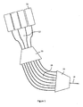
- Figure 1 shows an exemplary schematic view of a PIC comprising a plurality of electro-optical converters 11 (e.g. four discrete CWDM lasers) and an AWG multiplexer.
- the AWG multiplexer may comprise a plurality of waveguides 12, a first multimode section 13, a plurality of arrayed waveguides 16, a second multimode section 16 and an output waveguide 14.
- the electro-optical converters 11 are configured to convert electronic signals to optical signals, e.g. pulses of light at a specific wavelength.
- Light from the electro-optical converters 11 propagates through the first plurality of waveguides 12 and enters the first multimode section 13. From the first multimode section 13, the light enters the arrayed waveguides 16.
- the arrayed waveguides 16 are of different length so that an interference pattern is produced at the second multimode section 16.
- the plurality of waveguides 12, the first multimode section 13 and the plurality of arrayed waveguides 16 are arranged so that the produced interference pattern focuses the signals into the output waveguide 14 (e.g. a multimode waveguide).
- AWG based multiplexers may lead to low multiplexing losses.
- the AWG based multiplexers can be scaled for a higher number of channels, i.e. for a higher number of different CWDM wavelengths,
- this solution may be very costly as (i) the hybrid integration may require delicate alignment between passive and active waveguides and components; and as (ii) the monolithic integration may lead to large PIC-chip dimensions.
- MMI multimode interference
- a MMI multiplexer may be built as a PIC, where the light coming from a plurality of input fibers propagates through a multimode waveguide section into an output waveguide (e.g. an optical fiber).
- the basis of MMI multiplexers is the self-imaging principle of MMI. That is to say, by selecting the width and length of the multimode waveguide section, self-images of the different wavelengths can be coupled into the output waveguide.
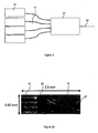
- FIGS 2 and 2a show schematic exemplary views of an MMI multiplexer in combination with a plurality of electro-optical converters 21 (e.g. four CWDM lasers).
- the MMI multiplexer may comprise a plurality of waveguides 22, a multimode section 23 and an output waveguide 24.
- the electro-optical converters 21 are configured to convert electronic signals to optical signals, e.g. pulses of light at specific wavelengths.
- the electro-optical converters 21 may be distributed feedback (DFB) lasers.
- the light from the electro-optical converters 21 propagates through the plurality of waveguides 22 and enters the multimode section 23.
- the plurality of waveguides 22 corresponds to a plurality of S-bend waveguides.
- Each mode in the multimode section 23 propagates with a different phase velocity and hence an interference pattern is produced that is dependent on the position along the multimode section 23.
- the electro-optical converters 21 are laterally positioned such that the curvature of each waveguide 22 does not exceed a predefined threshold in order to avoid signal losses.
- the curvature radius is preferably sufficiently large.
- the electro-optical converters 21 are laterally offset and the length of the S-bend waveguide 22 leading from a respective converter 21 to the multimode section 23 may be selected such that the losses due to the S-bends are kept below the predefined threshold.
- the PIC comprising four CWDM lasers and an MMI multiplexer to generate four optical channels as depicted in Figs. 2 and 2a may require around 2 mm 2 per device. That is to say, up to 3500 devices comprising the CWDM lasers and the MMI multiplexer may be manufactured from a 4 inch wafer.
- the multiplexing losses of the MMI multiplexer are at around 6 dB, which can be compensated with a booster.
- the size of the device will roughly have to be multiplied by 4 to maintain the same curvature radius of the S-bend waveguides 22.
- the MMI multiplexer losses may be greater than 9 dB, and the passive waveguides of the MMI multiplexer may be much longer. As a consequence, the fabrication yield and the multiplexing losses might become prohibitive when increasing the number of laterally placed DFB lasers (i.e. converters 21).
- FIG. 3 shows a schematic view of an MMI multiplexer using both parallel multiplexing as outlined in the context of Figs, 2 and 2a and serial multiplexing.
- the converters 21 are replaced by groups of converters 31aa, 31ab and 31ba, 31bb placed in series along the signal path.
- Fig. 3 illustrates two branches or groups of two converters 31aa, 31ab and 31ba, 31bb which are configured to generate light at different wavelengths.
- an MMI multiplexer may be used to multiplex the light coming from the plurality of electro-optical converters 31aa, 31ab, 31ba, 31bb.
- the MMI multiplexer preferably comprises a plurality of (S-bend) waveguides 32, a multimode section 33 and an output waveguide 34.
- the multimode section 33 may be arranged such that light from the plurality of waveguides 32 is multiplexed into the output waveguide 34, e.g, by using the self-imaging effect as described with reference to Figure 2 .
- the electro-optical converters 31aa, 31ab, 31ba, 31bb may be light emitting apparatuses.
- the light emitting apparatuses may be light emitting diodes (LED) or lasers.
- the lasers may be distributed feedback laser (DFB) lasers.
- the lasers may be directly modulated lasers (DML) or lasers using electro-absorption modulation (EAM), i.e. so called Electro-Absorption Modulated Lasers (EML).
- the material used for such converters 31aa, 31ab, 31ba, 31bb may be semiconductor material, such as Gallium arsenide, indium phosphide, gallium antimonide, and gallium nitride.
- Fig. 3 shows an arrangement where serial multiplexing of wavelengths is used in addition to parallel multiplexing based on MMI multiplexing.
- a given number of CWDM wavelengths can be multiplexed onto an output waveguide 34 using smaller MMI multiplexers which have tolerable multiplexing losses.
- the serial multiplexing is achieved by placing in series two or more electro-optical converters 31aa, 31ab.
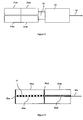
- the concept of serial multiplexing is outlined in the context of Fig. 4 which shows an embodiment of the converters 31aa, 31ab of Fig. 3 .
- the converters 31aa, 31ab comprise different active materials configured to convert an electrical signal into an optical signal. Furthermore, the converters 31aa and 31ab comprise an optical waveguide 37 for confining the emitted optical signal.
- the optical waveguide 37 traverses the two converters 31aa, 31ab. In particular, the waveguide 37 traverses a first active material of the first converter 31aa and a second active material of the second converter 31ab.
- light signals at the first wavelength and light signals at the second wavelength may be generated simultaneously within the waveguide 37, i.e. the light signals may be serially multiplexed onto the waveguide 37 of the converters 31aa, 31ab.
- Waveguide 37 may be connected to the waveguide 32a which corresponds to one of the waveguides 32 of the MMI multiplexer depicted In Fig. 3 .
- the waveguide 37 may be a single-mode waveguide, even for the short wavelengths carried by the waveguide 37.
- light emitted from the first and second active materials may be light of wavelengths in the wavelength interval of about 1450nm to about 1750 nm.
- parallel and serial multiplexing of the light generated by the electro-optical converters may be used, in order to design multi-wavelength CWDM emitters with a large numbers of optical channels, i.e. with a large number of CWDM wavelengths.
- this kind of serial multiplexing is feasible in the context of CWDM because of the large wavelength difference between different CWDM channels, which reduces the optical crosstalk between channels which are serially multiplexed.
- the second material used in the second converter 31ab is preferably selected such that light at the first wavelength passes through with low losses. Therefore, appropriate electro-optical materials for the first 31aa and the second 31ab converter may be selected. In an embodiment, the material of the first 31aa and second 31ab converter are selected such that the second wavelength is smaller than the first wavelength. In addition to designing the materials to emit a particular wavelength, the materials may be designed such that light at higher wavelengths than the particular emitted wavelength passes through the electro-optical material unaffected. As such, the second material of the second converter31ab may be designed to emit the second wavelength and it may be designed to not attenuate light at higher wavelengths than the second wavelength (e.g. light at the first wavelength).
- the material of the first converter 31aa may be selected such that light at the second wavelength, i.e. light at wavelengths which are lower than the first wavelength, is absorbed.
- electro-optical materials such as semiconductor materials comprising Indium (In), Gallium (Ga), Aluminium (AI), Arsenide (As) and/or Phosphorous (P).
- the first 31aa and second 31ab converter may comprise a first 36aa and a second 36ab grating, respectively, in order to provide DFB lasers.
- the first grating 36aa may have a grating period which allows for lasing at the first wavelength.
- the first 36aa and second 36ab gratings may be implemented as periodic variations of the refractive index of the material of the converter waveguide 37. The periodic variations of the refractive index are illustrated in Fig. 4 by a periodic succession of black and white sections of converter waveguide 37.
- the first 36aa and second 36ab gratings may have grating periods which allow for lasing at the first and second wavelength, respectively.
- the second grating 36ab may be transparent to the first wavelength.
- first 31aa and second 31ab converter may comprise a first 35aa and second 35ab rear reflector, respectively.
- the rear reflectors 35aa, 35ab may be configured to reflect the light emitted by the respective converter 31aa, 31ab, i.e. the light at the first and second wavelength, respectively.
- the second rear reflector 35ab i.e. the rear reflector of the second converter 31ab, may be configured to let pass (a high percentage, e.g. more than 50%, of) the light at the first wavelength.
- the light at the first and second wavelengths travels downstream towards the waveguide 32a. As such, the backward crosstalk between the different wavelengths can be reduced. Furthermore, the overall efficiency of the lasers can be improved.
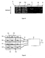
- FIG. 5 shows an example of a 4-to-1 MMI multiplexer and 4 pairs of serially multiplexed converters 31aa, 31ab.
- a multi-wavelength CWDM emitter using parallel and serial multiplexing is illustrated.
- 8 CWDM channels are multiplexed and the chip dimensions may be about 0.85*3 mm 2 .
- the dimensions were preferably about 0.85*2.5 mm 2 . That means that although the CWDM emitter according to Figure 5 multiplexes 8 channels, i.e.
- serial multiplexing does not substantially increase the multiplexing losses.
- the use of serial multiplexing may limit the increase in dimension and multiplexing losses compared to the increase in dimension (typically 400%) and the increase in multiplexing losses which are encountered when using only parallel multiplexing (e.g. when moving from a 4 channel MMI multiplexer to an 8 channel MMI multiplexer).
- the different wavelengths generated by the converters 31aa, 31ab may be arranged such that the wavelength difference between serially multiplexed wavelengths is high. This can be achieved by selecting four neighbouring wavelengths (1417nm, 1491nm, 1511nm, 1531nm) for parallel multiplexing and by serially multiplexing the following four wavelengths with the respective other wavelengths (1551nm, 1571nm, 1591nm, 1611nm). This is illustrated in Fig. 5 . By attributing the wavelengths to serial and parallel multiplexing in such a manner, the difference between wavelengths which are serially multiplexed can be maximized.
- the CWDM wavelengths are spaced by about 20 nm such that a large channel spacing of about 80 nm between adjacent serially multiplexed emitters can be achieved, thereby reducing the crosstalk.
- the material of the different converters is preferably selected appropriately.
- the material used for emitting light at about 1471 nm (resp. 1491nm, 1511nm and 1531nm), i.e. the material used for the second converter 31ab may be transparent to the light at about 1551 nm (resp. 1571nm, 1591nm and 1611nm), i.e. to the light emitted in the first converter 31aa. By doing this, the multiplexing losses caused by the serial multiplexing can be reduced. Furthermore, the material used for emitting light at about 1551 nm (resp. 1571nm, 1591nm and 1611nm), i.e.
- the material used for the first converter 31aa could completely absorb the emission at about 1471 nm (resp. 1491nm, 1511nm and 1531nm), i.e. the light emitted in the second converter 31ab. By doing this, the backward crosstalk could be reduced.
- a negatively biased section, or a reflector as outlined above may be introduced between the adjacent converters 31aa and 31ab in order to further reduce the backward crosstalk.
- T N comprises the lowest wavelengths
- T 1 comprises the highest wavelengths.
- Each active material M n may be configured to emit light at a wavelength ⁇ n belonging to the wavelength interval T n , respectively. It is assumed that material M N is positioned at the output end of the succession of converters C n and that material M 1 is positioned at the input or rear end, opposite or upstream to the output end, of the serially connected converters C n .
- material M N is positioned at the output end of waveguide W 37 and material M 1 is positioned at the rear end of waveguide W 37.
- Each active material M i is configured to leave unaffected light at a wavelength ⁇ j belonging to the wavelength interval T j , for j ⁇ i.
- each active material M i may be configured to absorb light at a wavelength ⁇ j belonging to the wavelength interval T j , for j>i.
- the light emitted by material M i passes through materials M i+1 ,...,M N , without being attenuated, in order to reach the output end of the waveguide W 37. Consequently, the serial multiplexing can be performed with low multiplexing losses.
- the light emitted by material M i which travels towards the rear end of the waveguide W 37 i.e. which travels towards materials M i-1 ,...,M 1 will be absorbed, thereby reducing backward crosstalk.
- the reflectors R n may be placed at the rear end of a converter C n .
- Each reflector R n may be configured to reflect wavelengths ⁇ n from the wavelengths interval T n .
- each reflector R n may be configured to let pass wavelengths ⁇ j from the wavelengths interval T j , for j ⁇ n.
- the same or other reflectors may be used for providing converters C n which comprise laser cavities.
- a serial connection of converters C n has been described in more general terms.
- a plurality of K such serial groups of converters may be placed in parallel, i.e. K such serial connections of converters may be placed in parallel onto a PIC, as shown e.g. in Fig.5 .
- the K output signals of the waveguides W k 37 may be optically multiplexed using parallel multiplexing, e.g. MMI multiplexing or AWG multiplexing.
- the serial multiplexing may be achieved by selecting appropriate active materials M kn .
- the wavelengths may be arranged within the matrix of converters C kn such that for some or all pairs of neighboring converters C ki , C kl+1 of a group of serial converters along waveguide W k , there are K-1 wavelengths ⁇ kn which are greater than wavelength ⁇ kl+1 emitted by converter C ki+1 and smaller than wavelength ⁇ kl emitted by converter C kj .
- this may be achieved by arranging the converter within the matrix such that ⁇ kn > ⁇ in , for k>i, and ⁇ kn > ⁇ ki , for i>n.
- Figure 6 shows an exemplary schematic view of an arrangement where three wavelengths are multiplexed in series in four groups 31a, 31b, 31c, 31d of converters prior to performing parallel multiplexing using a 4-to-1 MMI multiplexer.
- the MMI multiplexer may comprise a plurality of waveguides 32, a multimode section 33 and an output waveguide 34.
- the groups 31a, 31b, 31c, 31d of electro-optical converters comprise waveguides 37a, 37b, 37c, 37d which traverse the three converters 31aa-31ac, 31ba-31bc, 31ca-31cc and 31da-31dc, respectively.
- Each waveguide 37a, 37b, 37c, 37d traverses or passes through three different active materials, i.e. one active material per converter 31aa-31ac, 31ba-31bc, 31ca-31cc and 31da-31dc.
- each group 31a, 31b, 31c, 31d of converters emits three multiplexed CWDM wavelengths which are subsequently multiplexed using a 4-to-1 MMI multiplexer.
- a method and system of multiplexing light at different wavelengths has been described.
- a CWDM transmitter has been described which makes use of serial multiplexing of a plurality of wavelengths.
- serial multiplexing may be combined with parallel multiplexing (e.g. using MMI multiplexers or AWG multiplexers).
- parallel multiplexing e.g. using MMI multiplexers or AWG multiplexers.
- CWDM transmitters with a high degree of circuit integration may be provided.
- Such CWDM transmitters may be implemented as PICs for the use in optical access networks.
- any block diagrams herein represent conceptual views of illustrative circuitry embodying the principles of the invention.
- any flow charts, flow diagrams, state transition diagrams, pseudo code, and the like represent various processes which may be substantially represented in computer readable medium and so executed by a computer or processor, whether or not such computer or processor is explicitly shown.
Landscapes
- Physics & Mathematics (AREA)
- Optics & Photonics (AREA)
- General Physics & Mathematics (AREA)
- Electromagnetism (AREA)
- Condensed Matter Physics & Semiconductors (AREA)
- Engineering & Computer Science (AREA)
- Signal Processing (AREA)
- Computer Networks & Wireless Communication (AREA)
- Microelectronics & Electronic Packaging (AREA)
- Semiconductor Lasers (AREA)
- Optical Communication System (AREA)
- Optical Integrated Circuits (AREA)
- Lasers (AREA)
- Optical Couplings Of Light Guides (AREA)
Claims (14)
- Optischer Sender, konfiguriert für die Erzeugung einer Vielzahl von optischen Signalen mit einer entsprechenden Vielzahl von unterschiedlichen Wellenlängen, welche auf einen Ausgangswellenleiter (34) gemultiplext werden; wobei der Sender umfasst:- Einen ersten (31aa) und einen zweiten (31ab) Konverter mit unterschiedlichen ersten und zweiten Aktivmaterialien, konfiguriert für das Aussenden von Licht jeweils mit einer ersten und einer unterschiedlichen zweiten Wellenlänge; wobei das erste Aktivmaterial dafür konfiguriert ist, das Licht mit der zweiten Wellenlänge zu absorbieren, und wobei die zweite Wellenlänge kleiner als die erste Wellenlänge ist; und- einen ersten Konverter-Wellenleiter (37a), welcher das erste und das zweite Material des ersten (31aa) und des zweiten (31ab) Konverters durchquert, wobei sich das zweite Material an einem Ausgangsende des ersten Konverter-Wellenleiters (37a) und das erste Material an einem Eingangsende, stromaufwärts des Ausgangsendes, des ersten Konverter-Wellenleiters (37) befindet; wobei das zweite Aktivmatehal für das Licht mit der ersten Wellenlänge durchlässig ist, und wobei das Ausgangsende des ersten Konverter-Wellenleiters (37a) an den Ausgangswellenleiter (34) gekoppelt ist.
- Sender nach Anspruch 1 (of claim 1), wobei der erste Konverter (31aa) einen ersten Laser umfasst, welcher das erste Aktivmaterial benutzt, und wobei der zweite Konverter (31ab) einen zweiten Laser umfasst, welcher das zweite Aktivmaterial benutzt.
- Sender nach einem beliebigen der vorstehenden Ansprüche, wobei der erste Konverter (31aa) ein erstes Gitter (36aa) mit einer ersten Gitterperiode, welche mit der ersten Wellenlänge assoziiert ist, umfasst, und wobei der zweite Konverter (31 ab) ein zweites Gitter (36ab) mit einer zweiten Gitterperiode, welche mit der zweiten Wellenlänge assoziiert ist, umfasst.
- Sender nach einem beliebigen der vorstehenden Ansprüche, weiterhin umfassend:- Einen halbdurchlässigen Reflektor (36ab), welcher an einem Ausgangsende des ersten Konverters (31aa) und an einem Eingangsende des zweiten Konverters (31ab) angeordnet ist, wobei der halbdurchlässige Reflektor (36ab) im Wesentlichen für Licht mit der zweiten Wellenlänge reflektierend ist.
- Sender nach einem beliebigen der vorstehenden Ansprüche, wobei- Das erste und das zweite Material Halbleitermaterialien aus einer Gruppe, welche Gallium, Indium, Aluminium, Phosphor und/oder Arsenid umfasst, sind; und- der Sender eine photonische integrierte Schaltung ist.
- Sender nach einem beliebigen der vorstehenden Ansprüche, wobei der Sender ein optischer Sender für grobes Wellenlängenmultiplexing ist.
- Sender nach einem beliebigen der vorstehenden Ansprüche, wobei- Der Sender K Gruppen (31a, 31b, 31c, 31d) von N Konvertern Ckn, k=1,...,K und n=1,...,N mit K>1 und N>1 umfasst; wobei jede Gruppe für die Erzeugung eines seriell gemultiplexten optischen Signals Sk, umfassend N optische Signale mit Wellenlängen λkn, n=1,...,N, welche auf einen Konverter-Weilenleiter Wk gemultiplext werden, konfiguriert ist;- die Konverter Ckn unterschiedliche Aktivmaterialien Mkn umfassen, welche jeweils für das Aussenden von Licht mit der Wellenlänge λkn konfiguriert sind;- der erste (31 aa) und der zweite (31 ab) Konverter jeweils den Konvertern C11 und C12 entsprechen;- das erste und das zweite Aktivmaterial jeweils den Materialien M11 und M12 entsprechen,- der erste Konverter-Wellenleiter (37a) dem Konverter-Wellenleiter W1 der ersten Gruppe von N optischen Konvertern C1n entspricht;- die Konverter-Wellenleiter Wk, k=1,...K die N Aktivmaterialien Mkn, n=1,...,N der k-ten Gruppe von optischen Konvertern durchqueren; wobei sich das Material Mkn an einem Ausgangsende des Wellenleiters Wk und das Material Mk1 an einem Eingangsende, stromaufwärts des Ausgangsendes, des Wellenleiters Wk befindet;- das Material Mki dafür konfiguriert ist, für Licht mit einer Wellenlänge λkj, mit j<i, durchlässig zu sein; und- das Material Mki dafür konfiguriert ist, Licht mit einer Wellenlänge λkj, mit j>i, zu absorbieren; und- der Sender einen optischen Kombinator (32, 33) umfasst, welcher dafür konfiguriert ist, die K seriell gemultiplexten optischen Signale Sk am Ausgangsende der K Konverter-Wellenleiter Wk auf den Ausgangswellenleiter (34) zu multiplexen.
- Sender nach Anspruch 7, wobei- Die Konverter Ckn Gitter Gkn mit Gitterperioden von jeweils Λkn umfassen;- das erste (36aa) und das zweite (36ab) Gitter jeweils den Gittern G11 und G12 entsprechen; und- die Gitterperioden Λkn mit den Wellenlängen Λkn des von den entsprechenden Konvertern Ckn ausgesendeten Lichts assoziiert sind.
- Sender nach einem beliebigen der Ansprüche 7 bis 8, wobei- Die K Gruppen von Konvertern Ckn in einem seitlichen Abstand voneinander angeordnet sind, so dass sich die Ausgangsenden der K Kombinator-Wellenleiter Wk in einem seitlichen Abstand zueinander befinden;- der Kombinator einen ersten Zusammenführungsbereich (32) umfasst, wobei sich der seitliche Abstand zwischen den K Kombinator-Wellenleitern Wk zunehmend verringert; und- der Kombinator einen zweiten Zusammenführungsbereich (33) umfasst, wobei die seriell gemultiplexten optischen Signale Sk innerhalb eines gemeinsamen Wellenleiters, welcher zu dem Ausgangswellenleiter führt, überlagert werden.
- Sender nach Anspruch 9, wobei der erste Zusammenführungsbereich (32) eine Vielzahl von S-Bogen-Wellenleitern umfasst, welche für das zunehmende Verringern des Abstands zwischen den K Kombinator-Wellenleltern Wk konfiguriert sind.
- Sender nach einem beliebigen de Ansprüche 7 bis 10, wobei der Kombinator (32, 33) ein Multimode-Interferenzkoppler ist.
- Sender nach einem beliebigen der Ansprüche 7 bis 11, wobei die Aktivmaterialien Mkn und die entsprechenden Wellenlängen λkn derart ausgebildet sind, dass für mindestens ein Paar von benachbarten Konvertern Ckl, Ckl+1 der k-ten Gruppe von Konvertern entlang des Kombinator-Wellenleiters Wk K-1 Wellenlängen des Satzes von Wellenlängen λkn, k=1,,..,K und n=1,...,N vorhanden sind, welcher größer als die von dem Konverter Cki+1 ausgegebene Wellenlänge λki+1 und kleiner als die von dem Konverter Cki ausgegebene Wellenlänge λki sind.
- Sender nach Anspruch 12, wobei die Aktivmaterialien Mkn und die entsprechenden Wellenlängen λkn derart ausgebildet sind, dass λkn> λin für jeden beliebigen k>i, und λkn> λki für jeden beliebigen i>n.
- Verfahren zur Erzeugung einer Vielzahl von optischen Signalen mit einer entsprechenden Vielzahl von unterschiedlichen Wellenlängen, welche auf einen Ausgangswellenleiter gemultiplext werden; wobei das Verfahren umfasst:- Bereitstellen eines ersten (31aa) und eines zweiten (31ab) Konverters mit unterschiedlichen ersten und zweiten Aktivmaterialien, konfiguriert für das Aussenden von Licht mit einer ersten und einer unterschiedlichen zweiten Wellenlänge; wobei das erste Aktivmaterial dafür konfiguriert ist, das Licht mit der zweiten Wellenlänge zu absorbieren, und wobei die zweite Wellenlänge kleiner als die erste Wellenlänge ist; und- Bereitstellen eines ersten Konverter-Wellenleiters (37a), welcher das erste und das zweite Material des ersten (31aa) und des zweiten (31 ab) Konverters durchquert, wobei sich das zweite Material an einem Ausgangsende des ersten Konverter-Wellenleiters (37a) und das erste Material an einem Eingangsende, stromaufwärts des Ausgangsendes, des ersten Konverter-Wellenleiters (37a) befindet; wobei das zweite Aktivmaterial für das Licht mit der ersten Wellenlänge durchlässig ist, und wobei das Ausgangsende des ersten Konverter-Wellenteiters (37a) an den Ausgangswellenleiter (34) gekoppelt ist.
Priority Applications (8)
| Application Number | Priority Date | Filing Date | Title |
|---|---|---|---|
| EP10290509.8A EP2434594B1 (de) | 2010-09-27 | 2010-09-27 | Photonische integrierte Schaltung für Wellenlängenmultiplex-Verfahren |
| SG2013021209A SG189049A1 (en) | 2010-09-27 | 2011-09-23 | Photonic integrated circuit for wavelength division multiplexing |
| US13/824,736 US20140147129A1 (en) | 2010-09-27 | 2011-09-23 | Photonic integrated circuit for wavelength division multiplexing |
| KR1020137010602A KR20130058756A (ko) | 2010-09-27 | 2011-09-23 | 파장 분할 다중화용 광 집적 회로 |
| PCT/EP2011/066586 WO2012041776A1 (en) | 2010-09-27 | 2011-09-23 | Photonic integrated circuit for wavelength division multiplexing |
| JP2013529661A JP2013542594A (ja) | 2010-09-27 | 2011-09-23 | 波長分割多重化用フォトニック集積回路 |
| CN2011800466631A CN103125053A (zh) | 2010-09-27 | 2011-09-23 | 用于波分复用的光子集成电路 |
| TW100134628A TWI472108B (zh) | 2010-09-27 | 2011-09-26 | 用於波長分割多工之光子積體電路 |
Applications Claiming Priority (1)
| Application Number | Priority Date | Filing Date | Title |
|---|---|---|---|
| EP10290509.8A EP2434594B1 (de) | 2010-09-27 | 2010-09-27 | Photonische integrierte Schaltung für Wellenlängenmultiplex-Verfahren |
Publications (2)
| Publication Number | Publication Date |
|---|---|
| EP2434594A1 EP2434594A1 (de) | 2012-03-28 |
| EP2434594B1 true EP2434594B1 (de) | 2014-05-14 |
Family
ID=43564924
Family Applications (1)
| Application Number | Title | Priority Date | Filing Date |
|---|---|---|---|
| EP10290509.8A Not-in-force EP2434594B1 (de) | 2010-09-27 | 2010-09-27 | Photonische integrierte Schaltung für Wellenlängenmultiplex-Verfahren |
Country Status (8)
| Country | Link |
|---|---|
| US (1) | US20140147129A1 (de) |
| EP (1) | EP2434594B1 (de) |
| JP (1) | JP2013542594A (de) |
| KR (1) | KR20130058756A (de) |
| CN (1) | CN103125053A (de) |
| SG (1) | SG189049A1 (de) |
| TW (1) | TWI472108B (de) |
| WO (1) | WO2012041776A1 (de) |
Families Citing this family (4)
| Publication number | Priority date | Publication date | Assignee | Title |
|---|---|---|---|---|
| CN106605340B (zh) * | 2015-08-18 | 2020-07-10 | 古河电气工业株式会社 | 光半导体装置 |
| CN112639624B (zh) | 2018-08-29 | 2024-04-30 | Asml控股股份有限公司 | 紧凑型对准传感器布置 |
| JP7326006B2 (ja) * | 2019-04-12 | 2023-08-15 | 日本ルメンタム株式会社 | 光半導体素子、光サブアセンブリ、及び光モジュール |
| CN111830628B (zh) * | 2020-07-24 | 2022-06-28 | 联合微电子中心有限责任公司 | 粗波分复用/解复用器及光通信设备 |
Family Cites Families (13)
| Publication number | Priority date | Publication date | Assignee | Title |
|---|---|---|---|---|
| JPS6027197B2 (ja) * | 1977-08-04 | 1985-06-27 | 日本電気株式会社 | 集積化光源 |
| US4980892A (en) * | 1989-05-30 | 1990-12-25 | At&T Bell Laboratories | Optical system including wavelength-tunable semiconductor laser |
| US5031188A (en) * | 1990-04-30 | 1991-07-09 | At&T Bell Laboratories | Inline diplex lightwave transceiver |
| US5082343A (en) * | 1990-12-20 | 1992-01-21 | At&T Bell Laboratories | Isolated optical coupler |
| JP3149961B2 (ja) * | 1991-01-30 | 2001-03-26 | キヤノン株式会社 | 多波長半導体レーザ素子及びその駆動方法 |
| FR2734676B1 (fr) * | 1995-05-23 | 1997-08-08 | Labeyrie Antoine | Procede et dispositifs d'emission ou reception laser pour la transmission d'informations par voie optique |
| JP2842387B2 (ja) * | 1996-07-01 | 1999-01-06 | 日本電気株式会社 | 半導体光集積素子の製造方法 |
| US6104739A (en) * | 1997-12-24 | 2000-08-15 | Nortel Networks Corporation | Series of strongly complex coupled DFB lasers |
| JP2003014963A (ja) * | 2001-06-27 | 2003-01-15 | Nec Corp | 半導体光集積素子とその製造方法並びに光通信用モジュール |
| AU2002361565A1 (en) * | 2001-10-09 | 2003-04-22 | Infinera Corporation | Transmitter photonic integrated circuit (txpic) chip with enhanced power and yield without on-chip amplification |
| JP2003179315A (ja) * | 2001-12-12 | 2003-06-27 | Seiko Epson Corp | 光モジュールおよび光通信システム |
| JP2003195125A (ja) * | 2001-12-27 | 2003-07-09 | Seiko Epson Corp | 光モジュールおよび光通信システム |
| US7376165B2 (en) * | 2004-01-30 | 2008-05-20 | Bayerische Motoren Werke Aktiengesellschaft | Laser diode alignment and packaging system for integrated optical and display subassemblies |
-
2010
- 2010-09-27 EP EP10290509.8A patent/EP2434594B1/de not_active Not-in-force
-
2011
- 2011-09-23 KR KR1020137010602A patent/KR20130058756A/ko not_active Ceased
- 2011-09-23 US US13/824,736 patent/US20140147129A1/en not_active Abandoned
- 2011-09-23 SG SG2013021209A patent/SG189049A1/en unknown
- 2011-09-23 JP JP2013529661A patent/JP2013542594A/ja active Pending
- 2011-09-23 WO PCT/EP2011/066586 patent/WO2012041776A1/en not_active Ceased
- 2011-09-23 CN CN2011800466631A patent/CN103125053A/zh active Pending
- 2011-09-26 TW TW100134628A patent/TWI472108B/zh not_active IP Right Cessation
Also Published As
| Publication number | Publication date |
|---|---|
| SG189049A1 (en) | 2013-05-31 |
| CN103125053A (zh) | 2013-05-29 |
| US20140147129A1 (en) | 2014-05-29 |
| EP2434594A1 (de) | 2012-03-28 |
| TW201232976A (en) | 2012-08-01 |
| TWI472108B (zh) | 2015-02-01 |
| WO2012041776A1 (en) | 2012-04-05 |
| JP2013542594A (ja) | 2013-11-21 |
| KR20130058756A (ko) | 2013-06-04 |
Similar Documents
| Publication | Publication Date | Title |
|---|---|---|
| CN1127824C (zh) | 有关光传输的装置和方法 | |
| CN1483155A (zh) | 具有双向光服务信道的双向wdm光通信系统 | |
| JP7305556B2 (ja) | 集積wdm光トランシーバ | |
| KR100678245B1 (ko) | 수동형 광 가입자 망 | |
| WO2011120789A1 (en) | Photonic integrated transmitter | |
| US12549259B2 (en) | Photonic integrated circuit for high-wavelength-channel-count wavelength-division-multiplexed systems | |
| US7408701B2 (en) | Multi-frequency light source | |
| EP2434594B1 (de) | Photonische integrierte Schaltung für Wellenlängenmultiplex-Verfahren | |
| US20060008202A1 (en) | Light source apparatus for WDM optical communication and optical communication system | |
| US20230246725A1 (en) | Wavelength-Division-Multiplexing Optical Circuit Implemented in Photonic Integrated Circuit for Optical Transmitter | |
| US7031355B2 (en) | High efficiency single and multiple wavelength stabilized systems | |
| US7019907B2 (en) | Integrated lithium niobate based optical transmitter | |
| JP4230934B2 (ja) | 多チャンネル光変調装置および多チャンネル光送信装置 | |
| US20130094806A1 (en) | Optical signal conversion method and apparatus | |
| JP2014135588A (ja) | 波長多重ponシステム | |
| CN113411160B (zh) | 基于可切换波长连接(swc)的全光网 | |
| KR100611818B1 (ko) | 파장분할다중화용 양방향 통신을 위한 전송시스템 및 광모듈 | |
| ES2751632T3 (es) | Circuito integrado fotónico sintonizable emisor de longitud de onda múltiple | |
| US20230291493A1 (en) | Wavelength-Multiplexed Optical Source with Reduced Temperature Sensitivity | |
| Ao et al. | A waveguide-based bidirectional optical delay unit with Bragg reflectors | |
| EP1245997A1 (de) | Multifrequenz-Lichtquelle durch Vierwellenmischung | |
| JP3495665B2 (ja) | 多波長一括変換装置 | |
| Hoppe et al. | Enhanced Generalized Mach-Zehnder Interferometer for Tunable Channel Routing | |
| WO2021100070A1 (ja) | 光変調器、及び光送信器 | |
| KR20040023190A (ko) | 광전송 시스템용 다중 채널 분산 보상기 |
Legal Events
| Date | Code | Title | Description |
|---|---|---|---|
| PUAI | Public reference made under article 153(3) epc to a published international application that has entered the european phase |
Free format text: ORIGINAL CODE: 0009012 |
|
| AK | Designated contracting states |
Kind code of ref document: A1 Designated state(s): AL AT BE BG CH CY CZ DE DK EE ES FI FR GB GR HR HU IE IS IT LI LT LU LV MC MK MT NL NO PL PT RO SE SI SK SM TR |
|
| AX | Request for extension of the european patent |
Extension state: BA ME RS |
|
| 17P | Request for examination filed |
Effective date: 20120928 |
|
| 17Q | First examination report despatched |
Effective date: 20121107 |
|
| 111Z | Information provided on other rights and legal means of execution |
Free format text: AL AT BE BG CH CY CZ DE DK EE ES FI FR GB GR HR HU IE IS IT LI LT LU LV MC MK MT NL NO PL PT RO SE SI SK SM TR Effective date: 20130410 |
|
| REG | Reference to a national code |
Ref country code: DE Ref legal event code: R079 Ref document number: 602010016061 Country of ref document: DE Free format text: PREVIOUS MAIN CLASS: H01S0005062500 Ipc: G02B0006120000 |
|
| RIC1 | Information provided on ipc code assigned before grant |
Ipc: G02B 6/12 20060101AFI20131011BHEP Ipc: H01S 5/026 20060101ALI20131011BHEP Ipc: H01S 5/0625 20060101ALI20131011BHEP Ipc: H01S 5/12 20060101ALI20131011BHEP Ipc: H01S 5/40 20060101ALI20131011BHEP |
|
| GRAP | Despatch of communication of intention to grant a patent |
Free format text: ORIGINAL CODE: EPIDOSNIGR1 |
|
| INTG | Intention to grant announced |
Effective date: 20131204 |
|
| RIN1 | Information on inventor provided before grant (corrected) |
Inventor name: BRENOT, ROMAIN Inventor name: GARREAU, ALEXANDRE |
|
| GRAS | Grant fee paid |
Free format text: ORIGINAL CODE: EPIDOSNIGR3 |
|
| GRAA | (expected) grant |
Free format text: ORIGINAL CODE: 0009210 |
|
| AK | Designated contracting states |
Kind code of ref document: B1 Designated state(s): AL AT BE BG CH CY CZ DE DK EE ES FI FR GB GR HR HU IE IS IT LI LT LU LV MC MK MT NL NO PL PT RO SE SI SK SM TR |
|
| REG | Reference to a national code |
Ref country code: GB Ref legal event code: FG4D |
|
| REG | Reference to a national code |
Ref country code: AT Ref legal event code: REF Ref document number: 668700 Country of ref document: AT Kind code of ref document: T Effective date: 20140615 |
|
| REG | Reference to a national code |
Ref country code: IE Ref legal event code: FG4D |
|
| REG | Reference to a national code |
Ref country code: DE Ref legal event code: R096 Ref document number: 602010016061 Country of ref document: DE Effective date: 20140626 |
|
| REG | Reference to a national code |
Ref country code: CH Ref legal event code: PCOW Free format text: NEW ADDRESS: 148/152 ROUTE DE LA REINE, 92100 BOULOGNE-BILLANCOURT (FR) |
|
| RAP2 | Party data changed (patent owner data changed or rights of a patent transferred) |
Owner name: ALCATEL LUCENT |
|
| REG | Reference to a national code |
Ref country code: AT Ref legal event code: MK05 Ref document number: 668700 Country of ref document: AT Kind code of ref document: T Effective date: 20140514 Ref country code: NL Ref legal event code: VDEP Effective date: 20140514 |
|
| REG | Reference to a national code |
Ref country code: LT Ref legal event code: MG4D |
|
| PG25 | Lapsed in a contracting state [announced via postgrant information from national office to epo] |
Ref country code: IS Free format text: LAPSE BECAUSE OF FAILURE TO SUBMIT A TRANSLATION OF THE DESCRIPTION OR TO PAY THE FEE WITHIN THE PRESCRIBED TIME-LIMIT Effective date: 20140914 Ref country code: GR Free format text: LAPSE BECAUSE OF FAILURE TO SUBMIT A TRANSLATION OF THE DESCRIPTION OR TO PAY THE FEE WITHIN THE PRESCRIBED TIME-LIMIT Effective date: 20140815 Ref country code: LT Free format text: LAPSE BECAUSE OF FAILURE TO SUBMIT A TRANSLATION OF THE DESCRIPTION OR TO PAY THE FEE WITHIN THE PRESCRIBED TIME-LIMIT Effective date: 20140514 Ref country code: FI Free format text: LAPSE BECAUSE OF FAILURE TO SUBMIT A TRANSLATION OF THE DESCRIPTION OR TO PAY THE FEE WITHIN THE PRESCRIBED TIME-LIMIT Effective date: 20140514 Ref country code: CY Free format text: LAPSE BECAUSE OF FAILURE TO SUBMIT A TRANSLATION OF THE DESCRIPTION OR TO PAY THE FEE WITHIN THE PRESCRIBED TIME-LIMIT Effective date: 20140514 Ref country code: NO Free format text: LAPSE BECAUSE OF FAILURE TO SUBMIT A TRANSLATION OF THE DESCRIPTION OR TO PAY THE FEE WITHIN THE PRESCRIBED TIME-LIMIT Effective date: 20140814 |
|
| PGFP | Annual fee paid to national office [announced via postgrant information from national office to epo] |
Ref country code: DE Payment date: 20140922 Year of fee payment: 5 |
|
| PG25 | Lapsed in a contracting state [announced via postgrant information from national office to epo] |
Ref country code: LV Free format text: LAPSE BECAUSE OF FAILURE TO SUBMIT A TRANSLATION OF THE DESCRIPTION OR TO PAY THE FEE WITHIN THE PRESCRIBED TIME-LIMIT Effective date: 20140514 Ref country code: SE Free format text: LAPSE BECAUSE OF FAILURE TO SUBMIT A TRANSLATION OF THE DESCRIPTION OR TO PAY THE FEE WITHIN THE PRESCRIBED TIME-LIMIT Effective date: 20140514 Ref country code: HR Free format text: LAPSE BECAUSE OF FAILURE TO SUBMIT A TRANSLATION OF THE DESCRIPTION OR TO PAY THE FEE WITHIN THE PRESCRIBED TIME-LIMIT Effective date: 20140514 Ref country code: ES Free format text: LAPSE BECAUSE OF FAILURE TO SUBMIT A TRANSLATION OF THE DESCRIPTION OR TO PAY THE FEE WITHIN THE PRESCRIBED TIME-LIMIT Effective date: 20140514 Ref country code: PL Free format text: LAPSE BECAUSE OF FAILURE TO SUBMIT A TRANSLATION OF THE DESCRIPTION OR TO PAY THE FEE WITHIN THE PRESCRIBED TIME-LIMIT Effective date: 20140514 Ref country code: AT Free format text: LAPSE BECAUSE OF FAILURE TO SUBMIT A TRANSLATION OF THE DESCRIPTION OR TO PAY THE FEE WITHIN THE PRESCRIBED TIME-LIMIT Effective date: 20140514 |
|
| PGFP | Annual fee paid to national office [announced via postgrant information from national office to epo] |
Ref country code: FR Payment date: 20140919 Year of fee payment: 5 Ref country code: GB Payment date: 20140919 Year of fee payment: 5 |
|
| PG25 | Lapsed in a contracting state [announced via postgrant information from national office to epo] |
Ref country code: PT Free format text: LAPSE BECAUSE OF FAILURE TO SUBMIT A TRANSLATION OF THE DESCRIPTION OR TO PAY THE FEE WITHIN THE PRESCRIBED TIME-LIMIT Effective date: 20140915 |
|
| PG25 | Lapsed in a contracting state [announced via postgrant information from national office to epo] |
Ref country code: DK Free format text: LAPSE BECAUSE OF FAILURE TO SUBMIT A TRANSLATION OF THE DESCRIPTION OR TO PAY THE FEE WITHIN THE PRESCRIBED TIME-LIMIT Effective date: 20140514 Ref country code: EE Free format text: LAPSE BECAUSE OF FAILURE TO SUBMIT A TRANSLATION OF THE DESCRIPTION OR TO PAY THE FEE WITHIN THE PRESCRIBED TIME-LIMIT Effective date: 20140514 Ref country code: BE Free format text: LAPSE BECAUSE OF FAILURE TO SUBMIT A TRANSLATION OF THE DESCRIPTION OR TO PAY THE FEE WITHIN THE PRESCRIBED TIME-LIMIT Effective date: 20140514 Ref country code: SK Free format text: LAPSE BECAUSE OF FAILURE TO SUBMIT A TRANSLATION OF THE DESCRIPTION OR TO PAY THE FEE WITHIN THE PRESCRIBED TIME-LIMIT Effective date: 20140514 Ref country code: RO Free format text: LAPSE BECAUSE OF FAILURE TO SUBMIT A TRANSLATION OF THE DESCRIPTION OR TO PAY THE FEE WITHIN THE PRESCRIBED TIME-LIMIT Effective date: 20140514 Ref country code: CZ Free format text: LAPSE BECAUSE OF FAILURE TO SUBMIT A TRANSLATION OF THE DESCRIPTION OR TO PAY THE FEE WITHIN THE PRESCRIBED TIME-LIMIT Effective date: 20140514 |
|
| REG | Reference to a national code |
Ref country code: DE Ref legal event code: R097 Ref document number: 602010016061 Country of ref document: DE |
|
| PG25 | Lapsed in a contracting state [announced via postgrant information from national office to epo] |
Ref country code: NL Free format text: LAPSE BECAUSE OF FAILURE TO SUBMIT A TRANSLATION OF THE DESCRIPTION OR TO PAY THE FEE WITHIN THE PRESCRIBED TIME-LIMIT Effective date: 20140514 |
|
| PLBE | No opposition filed within time limit |
Free format text: ORIGINAL CODE: 0009261 |
|
| STAA | Information on the status of an ep patent application or granted ep patent |
Free format text: STATUS: NO OPPOSITION FILED WITHIN TIME LIMIT |
|
| 26N | No opposition filed |
Effective date: 20150217 |
|
| PG25 | Lapsed in a contracting state [announced via postgrant information from national office to epo] |
Ref country code: LU Free format text: LAPSE BECAUSE OF FAILURE TO SUBMIT A TRANSLATION OF THE DESCRIPTION OR TO PAY THE FEE WITHIN THE PRESCRIBED TIME-LIMIT Effective date: 20140927 Ref country code: IT Free format text: LAPSE BECAUSE OF FAILURE TO SUBMIT A TRANSLATION OF THE DESCRIPTION OR TO PAY THE FEE WITHIN THE PRESCRIBED TIME-LIMIT Effective date: 20140514 Ref country code: MC Free format text: LAPSE BECAUSE OF FAILURE TO SUBMIT A TRANSLATION OF THE DESCRIPTION OR TO PAY THE FEE WITHIN THE PRESCRIBED TIME-LIMIT Effective date: 20140514 |
|
| REG | Reference to a national code |
Ref country code: CH Ref legal event code: PL |
|
| REG | Reference to a national code |
Ref country code: DE Ref legal event code: R097 Ref document number: 602010016061 Country of ref document: DE Effective date: 20150217 |
|
| REG | Reference to a national code |
Ref country code: IE Ref legal event code: MM4A |
|
| PG25 | Lapsed in a contracting state [announced via postgrant information from national office to epo] |
Ref country code: CH Free format text: LAPSE BECAUSE OF NON-PAYMENT OF DUE FEES Effective date: 20140930 Ref country code: LI Free format text: LAPSE BECAUSE OF NON-PAYMENT OF DUE FEES Effective date: 20140930 Ref country code: SI Free format text: LAPSE BECAUSE OF FAILURE TO SUBMIT A TRANSLATION OF THE DESCRIPTION OR TO PAY THE FEE WITHIN THE PRESCRIBED TIME-LIMIT Effective date: 20140514 |
|
| PG25 | Lapsed in a contracting state [announced via postgrant information from national office to epo] |
Ref country code: IE Free format text: LAPSE BECAUSE OF NON-PAYMENT OF DUE FEES Effective date: 20140927 |
|
| REG | Reference to a national code |
Ref country code: DE Ref legal event code: R119 Ref document number: 602010016061 Country of ref document: DE |
|
| PG25 | Lapsed in a contracting state [announced via postgrant information from national office to epo] |
Ref country code: SM Free format text: LAPSE BECAUSE OF FAILURE TO SUBMIT A TRANSLATION OF THE DESCRIPTION OR TO PAY THE FEE WITHIN THE PRESCRIBED TIME-LIMIT Effective date: 20140514 |
|
| GBPC | Gb: european patent ceased through non-payment of renewal fee |
Effective date: 20150927 |
|
| PG25 | Lapsed in a contracting state [announced via postgrant information from national office to epo] |
Ref country code: MT Free format text: LAPSE BECAUSE OF FAILURE TO SUBMIT A TRANSLATION OF THE DESCRIPTION OR TO PAY THE FEE WITHIN THE PRESCRIBED TIME-LIMIT Effective date: 20140514 Ref country code: BG Free format text: LAPSE BECAUSE OF FAILURE TO SUBMIT A TRANSLATION OF THE DESCRIPTION OR TO PAY THE FEE WITHIN THE PRESCRIBED TIME-LIMIT Effective date: 20140514 |
|
| REG | Reference to a national code |
Ref country code: FR Ref legal event code: ST Effective date: 20160531 |
|
| PG25 | Lapsed in a contracting state [announced via postgrant information from national office to epo] |
Ref country code: HU Free format text: LAPSE BECAUSE OF FAILURE TO SUBMIT A TRANSLATION OF THE DESCRIPTION OR TO PAY THE FEE WITHIN THE PRESCRIBED TIME-LIMIT; INVALID AB INITIO Effective date: 20100927 Ref country code: TR Free format text: LAPSE BECAUSE OF FAILURE TO SUBMIT A TRANSLATION OF THE DESCRIPTION OR TO PAY THE FEE WITHIN THE PRESCRIBED TIME-LIMIT Effective date: 20140514 Ref country code: DE Free format text: LAPSE BECAUSE OF NON-PAYMENT OF DUE FEES Effective date: 20160401 Ref country code: GB Free format text: LAPSE BECAUSE OF NON-PAYMENT OF DUE FEES Effective date: 20150927 |
|
| PG25 | Lapsed in a contracting state [announced via postgrant information from national office to epo] |
Ref country code: FR Free format text: LAPSE BECAUSE OF NON-PAYMENT OF DUE FEES Effective date: 20150930 |
|
| PG25 | Lapsed in a contracting state [announced via postgrant information from national office to epo] |
Ref country code: MK Free format text: LAPSE BECAUSE OF FAILURE TO SUBMIT A TRANSLATION OF THE DESCRIPTION OR TO PAY THE FEE WITHIN THE PRESCRIBED TIME-LIMIT Effective date: 20140514 |
|
| PG25 | Lapsed in a contracting state [announced via postgrant information from national office to epo] |
Ref country code: AL Free format text: LAPSE BECAUSE OF FAILURE TO SUBMIT A TRANSLATION OF THE DESCRIPTION OR TO PAY THE FEE WITHIN THE PRESCRIBED TIME-LIMIT Effective date: 20140514 |