EP2426895A1 - Structure of case for portable electronic device, portable electronic device, and production method therefor - Google Patents
Structure of case for portable electronic device, portable electronic device, and production method therefor Download PDFInfo
- Publication number
- EP2426895A1 EP2426895A1 EP10769635A EP10769635A EP2426895A1 EP 2426895 A1 EP2426895 A1 EP 2426895A1 EP 10769635 A EP10769635 A EP 10769635A EP 10769635 A EP10769635 A EP 10769635A EP 2426895 A1 EP2426895 A1 EP 2426895A1
- Authority
- EP
- European Patent Office
- Prior art keywords
- opening
- electronic device
- case
- portable electronic
- rear case
- Prior art date
- Legal status (The legal status is an assumption and is not a legal conclusion. Google has not performed a legal analysis and makes no representation as to the accuracy of the status listed.)
- Granted
Links
Images



Classifications
-
- H—ELECTRICITY
- H05—ELECTRIC TECHNIQUES NOT OTHERWISE PROVIDED FOR
- H05K—PRINTED CIRCUITS; CASINGS OR CONSTRUCTIONAL DETAILS OF ELECTRIC APPARATUS; MANUFACTURE OF ASSEMBLAGES OF ELECTRICAL COMPONENTS
- H05K5/00—Casings, cabinets or drawers for electric apparatus
- H05K5/02—Details
- H05K5/03—Covers
-
- H—ELECTRICITY
- H04—ELECTRIC COMMUNICATION TECHNIQUE
- H04M—TELEPHONIC COMMUNICATION
- H04M1/00—Substation equipment, e.g. for use by subscribers
- H04M1/02—Constructional features of telephone sets
- H04M1/0202—Portable telephone sets, e.g. cordless phones, mobile phones or bar type handsets
- H04M1/0249—Details of the mechanical connection between the housing parts or relating to the method of assembly
-
- H—ELECTRICITY
- H04—ELECTRIC COMMUNICATION TECHNIQUE
- H04B—TRANSMISSION
- H04B1/00—Details of transmission systems, not covered by a single one of groups H04B3/00 - H04B13/00; Details of transmission systems not characterised by the medium used for transmission
- H04B1/38—Transceivers, i.e. devices in which transmitter and receiver form a structural unit and in which at least one part is used for functions of transmitting and receiving
- H04B1/3827—Portable transceivers
- H04B1/3833—Hand-held transceivers
- H04B1/3838—Arrangements for reducing RF exposure to the user, e.g. by changing the shape of the transceiver while in use
-
- H—ELECTRICITY
- H04—ELECTRIC COMMUNICATION TECHNIQUE
- H04M—TELEPHONIC COMMUNICATION
- H04M1/00—Substation equipment, e.g. for use by subscribers
- H04M1/02—Constructional features of telephone sets
- H04M1/0202—Portable telephone sets, e.g. cordless phones, mobile phones or bar type handsets
- H04M1/026—Details of the structure or mounting of specific components
-
- H—ELECTRICITY
- H04—ELECTRIC COMMUNICATION TECHNIQUE
- H04M—TELEPHONIC COMMUNICATION
- H04M1/00—Substation equipment, e.g. for use by subscribers
- H04M1/02—Constructional features of telephone sets
- H04M1/0202—Portable telephone sets, e.g. cordless phones, mobile phones or bar type handsets
- H04M1/0206—Portable telephones comprising a plurality of mechanically joined movable body parts, e.g. hinged housings
- H04M1/0208—Portable telephones comprising a plurality of mechanically joined movable body parts, e.g. hinged housings characterized by the relative motions of the body parts
- H04M1/0214—Foldable telephones, i.e. with body parts pivoting to an open position around an axis parallel to the plane they define in closed position
-
- Y—GENERAL TAGGING OF NEW TECHNOLOGICAL DEVELOPMENTS; GENERAL TAGGING OF CROSS-SECTIONAL TECHNOLOGIES SPANNING OVER SEVERAL SECTIONS OF THE IPC; TECHNICAL SUBJECTS COVERED BY FORMER USPC CROSS-REFERENCE ART COLLECTIONS [XRACs] AND DIGESTS
- Y10—TECHNICAL SUBJECTS COVERED BY FORMER USPC
- Y10T—TECHNICAL SUBJECTS COVERED BY FORMER US CLASSIFICATION
- Y10T29/00—Metal working
- Y10T29/49—Method of mechanical manufacture
- Y10T29/49826—Assembling or joining
Definitions
- the opening having a quadrangular shape whose size is somewhat larger than the external dimensions of the electronic component.
- the opening is formed as small as possible, thereby suppressing a decrease in mechanical strength in the rear case due to the formation of the opening.
- the rear case includes the quadrangular opening
- an external force such as an impact or a pressing force from the outside of the housing
- stress concentrates on the four corners of the opening. Consequently, cracking may occur in the four corners of the opening of the rear case, resulting in breakage of the rear case.
- a portable electronic device includes: a case structure for a portable electronic device according to the present invention; and a circuit board with an electronic component mounted thereon.
- a method for manufacturing a portable electronic device includes: forming a case member that has an opening, into which a part of an electronic component to be housed inside the case member is inserted; and forming a cover member arranged at a position where the cover member covers the opening of the case member.
- Forming a case member includes forming a recess portion extending from an inner peripheral surface of the opening toward an outer peripheral side of the opening at each corner of the opening.
- main display panel 17 for example, a liquid-crystal display panel or an organic EL (electroluminescence) display, is arranged.
- Main display panel 17 is covered by front panel 18.
- sub display panel 31 and LED 32 are arranged in rear case 12. Display on sub display panel 31 and a light-emission state of LED 32 can be viewed through rear panel 13b.
- portable telephone 1 includes rear case 12 that has quadrangular first opening 26 into which a part in a thickness direction of first electronic component 21 is inserted, and at respective corners of first opening 26 of rear case 12, recess portions 30 extending respective inner peripheral surfaces of first opening 26 toward respective outer peripheral sides of first opening 26 are provided.
- This configuration enables preventing a decrease in the mechanical strength of rear case 12, which occurs when first opening 26 of rear case 12 is formed so as to have the smallest possible opening area according to the size of first electronic component 21, as well as preventing a collision between the angulated corners of first electronic component 21 and the corners of first opening 26. Consequently, portable telephone 1 enables a decrease in thickness of the entire device as well as preventing breakage of rear case 12.
- the configuration according to the present invention is not limited to such configuration in which a rear case includes openings, and openings may be provided in another member that houses electronic components inside.
- a portable telephone employs a structure in which a support plate supporting a circuit board is arranged on the front case side, openings that include recess portions may be provided in the support plate.
Landscapes
- Engineering & Computer Science (AREA)
- Signal Processing (AREA)
- Microelectronics & Electronic Packaging (AREA)
- Computer Networks & Wireless Communication (AREA)
- Telephone Set Structure (AREA)
- Casings For Electric Apparatus (AREA)
Abstract
Description
- The present invention relates to a case structure for a portable electronic device including a case member housing an electronic component inside, a portable electronic device, and a method for manufacturing a portable electronic device.
- As an example of portable electronic devices, a folding portable telephone includes a receiver section-side housing in which a main display panel is arranged, and a transmitter section-side housing in which operation buttons are arranged, the receiver section-side housing and the transmitter section-side housing being pivotally connected via a hinge portion. The receiver section-side housing includes a combination of a pair of a front case and a rear case.
- As an example of a receiver section-side housing included in a portable telephone related to the present invention, there is a known configuration in which a rear cover, which is made of a transparent resin material, is attached to a rear case, which is made of an opaque resin material for decorative effect enhancement (see, for example, patent literature 1).
- Furthermore, where a portable electronic device employs a configuration in which light-emitting components such as LEDs (light-emitting diodes) and/or a sub display panel are arranged on the rear case side, a rear cover covers, these light-emitting components, is made of a light-transmissive material while a rear case is made of an opaque material.
- In addition, in order to provide two different types of decorative processing, for example, the housing of a portable telephone has a configuration in which a rear cover, to which decorative processing applied, which is different from decorative processing applied to a rear case, is attached to the rear case.
-
- Patent Literature 1:
JP2008-49621A Figure 3 ) - As described above, in recent years, portable telephones that include a structure in which a rear cover is attached to a rear case, are becoming increasingly thinner. In connection with that, in order to reduce the thickness of the housing to the extent equal to or exceeding an extent in which electronic components on a circuit board housed inside the housing and the rear cover interfere with each other, there has been proposed a configuration in which a rear case includes openings, into which parts of such components in a height (thickness) direction, i.e., a direction perpendicular to a mounting surface of a circuit board, are inserted, that is, "structure for preventing contact with a component". As described above, where an electronic component having a quadrangular shape on a plane parallel to a mounting surface of a circuit board is inserted into the opening of a rear case, the opening having a quadrangular shape whose size is somewhat larger than the external dimensions of the electronic component. As described above, the opening is formed as small as possible, thereby suppressing a decrease in mechanical strength in the rear case due to the formation of the opening.
- However, where the rear case includes the quadrangular opening, when an external force such as an impact or a pressing force from the outside of the housing is applied to the housing while the portable telephone is being handled, stress concentrates on the four corners of the opening. Consequently, cracking may occur in the four corners of the opening of the rear case, resulting in breakage of the rear case.
- In order to prevent such stress concentration, each of the four corners of the quadrangular opening can have a circular arc shape. However, where a quadrangular electronic component is inserted into the opening with its corner portions each having a circular arc shape, it is necessary to prevent interference between the angulated corner portions of the electronic component and the corner portions of the opening. Therefore, it is necessary to form the opening large according to the amount of interference between the angulated corner portions of the electronic component and the corners portions of the opening, which results in a decrease in the mechanical strength of the rear case in which the opening is formed.
- An object of the present invention to provide a case structure for a portable electronic device, a portable electronic device and a method for manufacturing the same, which can solve the aforementioned problem. An example of the object is to prevent breakage of a case member of a portable electronic device even though the portable electronic device is designed to be thinner.
- A case structure for a portable electronic device according to one aspect of the present invention includes: a case member that has a quadrangular opening into which a part of an electronic component, which is to be housed inside the case member, is inserted; and a cover member which is arranged at a position where the cover member covers the opening of the case member. Each corner portion of the opening of the case member includes a recess portion extending from an inner peripheral surface of the opening toward an outer peripheral side of the opening.
- Also, a portable electronic device according to the present invention includes: a case structure for a portable electronic device according to the present invention; and a circuit board with an electronic component mounted thereon.
- Also, a method for manufacturing a portable electronic device according to the present invention includes: forming a case member that has an opening, into which a part of an electronic component to be housed inside the case member is inserted; and forming a cover member arranged at a position where the cover member covers the opening of the case member. Forming a case member includes forming a recess portion extending from an inner peripheral surface of the opening toward an outer peripheral side of the opening at each corner of the opening.
- As described above, the present invention enables preventing breakage of a case member of a portable electronic device even though the portable electronic device is designed to be thinner.
-
- [
Figure 1] Figure 1 is a schematic diagram illustrating a portable telephone according to an exemplary embodiment. - [
Figure 2] Figure 2 is a perspective diagram illustrating a receiver section-side housing of a portable telephone according to an exemplary embodiment. - [
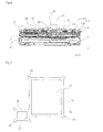
Figure 3] Figure 3 is a plan view illustrating a rear case included in a portable telephone according to an exemplary embodiment. - [
Figure 4] Figure 4 is a cross-sectional diagram along line A-A of the portable telephone according to the exemplary embodiment illustrated inFigure 3 . - [
Figure 5] Figure 5 is an enlarged plan view illustrating first and second openings of a rear case according to an exemplary embodiment. - [
Figure 6] Figure 6 is an enlarged view of recess portions included in first and second openings of a rear case according to an exemplary embodiment. - [
Figure 7] Figure 7 is a cross-sectional diagram illustrating a first opening of a rear case according to an exemplary embodiment. - Hereinafter, a specific exemplary embodiment of the present invention will be described with reference to the drawings.
- A portable telephone according to an exemplary embodiment will be described as an example of a portable electronic device according to the present invention. As illustrated in
Figures 1 and2 ,portable telephone 1 includes receiver section-side housing 6 in which a main display panel is arranged, and transmitter section-side housing 7 in which operation buttons 9 are arranged, receiver section-side housing 6 and transmitter section-side housing 7 being pivotally connected viahinge portion 8. - Receiver section-
side housing 6 includes a pair offront cases 11 andrear case 12, andrear cover 13, which is a cover member,rear cover 13 being assembled torear case 12, which is a cover member.Front case 11 andrear case 12 each is made of an opaque resin material.Rear cover 13 includesrear cover body 13a andrear panel 13b attached torear cover body 13a. Inrear cover 13,rear cover body 13a includes an opaque resin material, andrear panel 13b includes a light-transmissive resin material. - Also, as illustrated in
Figure 4 , in receiver section-side housing 6,circuit board 15 with electronic components 16 mounted thereon are arranged, and electronic components 16 are housed insiderear case 12. Furthermore, in receiver section side-housing 6,main display panel 17, for example, a liquid-crystal display panel or an organic EL (electroluminescence) display, is arranged.Main display panel 17 is covered byfront panel 18. - As illustrated in
Figures 2 and3 ,rear case 12 includes quadrangular first opening 26 into which a part in a thickness direction of firstelectronic component 21 to be housed insiderear case 12 is inserted. Also,rear case 12 includes rectangularsecond opening 27 into which a part in a thickness direction of secondelectronic component 22 oncircuit board 15 is inserted. As illustrated inFigure 5 , first and secondelectronic components circuit board 15, are inserted into first opening 26 and second opening 27, respectively, and the opening areas of first opening 26 andsecond opening 27 are different from each other. - Corner portions of first opening 26 and
second opening 27 includerespective recess portions 30 extending from respective inner peripheral surfaces of first andsecond openings second openings Rear case 12 including first andsecond openings recess portions 30 is integrally formed by a resin material. As illustrated inFigure 6 , for example, eachrecess portion 30 has a circular arc shape with point O, at which straight lines extending from two adjacent inner peripheral surfaces of respective first orsecond opening recess portion 30 are smoothly continuous with the inner peripheral surfaces of respectivesecond opening - As a result of
recess portions 30 being formed in such a manner as described above, no parts ofopenings electronic component openings openings side housing 6 is subjected to an external impact, whileportable telephone 1 is being handled, breakage can be prevented form occurring inopenings rear case 12. - The shape of each
recess portion 30 is not limited to the aforementioned circular arc shape, and any shape formed so as to prevent stress concentration and avoid collision of angular corners of an electronic component withrecess portion 30 can be employed. It should be understood that the shape of eachrecess portion 30 may be another shape such as, for example, a shape including an extension portion extending from a corner of an opening along a diagonal of the opening and a circular arc portion provided at an end of the extension portion. - Furthermore, as illustrated in
Figure 5 , first opening 26 andsecond opening 27 are provided in such a manner that adjacent inner peripheral surfaces thereof are partially connected to each other. As a result of first opening 26 andsecond opening 27 being connected to each other, the number ofrecess portions 30 provided at respective corners can be reduced. Thus, the moldability ofrear case 12 can be enhanced while structures for cavities that are contained in a mold forrear case 12 are simplified. - As illustrated in
Figure 7 , which is an enlarged view of a part ofFigure 4 , parts of first and secondelectronic components circuit board 15, are inserted inside first andsecond openings rear case 12. First and secondelectronic components rear panel 13b side from first andsecond openings - In
rear case 12, an edge portion of each of first andsecond openings rear panel 13b has a thickness of around 1 mm. - Furthermore, as illustrated in
Figures 3 and4 ,rear case 12 includes rectangularthird opening 28 into which a part on a side surface side of third electronic component 23 (right-side angulated corner inFigure 4 ) is inserted. As with first andsecond openings third opening 28 includesrecess portions 30 at respective corner portions thereof. - Furthermore,
rear case 12 includes slit-likefourth opening 29 into which a part on a side surface side of fourth electronic component 24 (left-side angulated corner inFigure 4 ) is inserted. As with first andsecond openings fourth opening 29 includesrecess portions 30 at respective corner portions thereof. - First to
fourth openings 26 to 29 ofrear case 12 are then covered byrear panel 13b ofrear cover 13.Rear panel 13b is bonded torear cover body 13a via an adhesive.Rear case 12 is bonded torear panel 13b via an adhesive. - Furthermore, as illustrated in
Figures 2 and3 ,sub display panel 31 andLED 32 are arranged inrear case 12. Display onsub display panel 31 and a light-emission state ofLED 32 can be viewed throughrear panel 13b. - Next, a method for manufacturing a portable telephone configured as described above will be described.
- A manufacturing method according to the present exemplary embodiment includes the steps of: forming
rear case 12 including first tofourth openings 26 to 29 into which parts of first to fourthelectronic component 21 to 24 to be housed insiderear case 12 are inserted; and formingrear cover 13 that includesrear panel 13b attached torear case 12,rear cover 13 covering first tofourth openings 26 to 29 ofrear case 12. - The step of forming
rear case 12 includes formingrecess portions 30 extending from respective inner peripheral surfaces ofopenings 26 to 29 toward respective outer peripheral sides ofopenings 26 to 29 at respective corner portions of first tofourth openings 26 to 29. The step of formingrear case 12 includes integrally moldingrear case 12 that hasrespective openings 26 to 29 in whichrecess portion 30 is formed, by means of a mold, using a resin material. - As described above,
portable telephone 1 includesrear case 12 that has quadrangularfirst opening 26 into which a part in a thickness direction of firstelectronic component 21 is inserted, and at respective corners offirst opening 26 ofrear case 12,recess portions 30 extending respective inner peripheral surfaces offirst opening 26 toward respective outer peripheral sides offirst opening 26 are provided. This configuration enables preventing a decrease in the mechanical strength ofrear case 12, which occurs whenfirst opening 26 ofrear case 12 is formed so as to have the smallest possible opening area according to the size of firstelectronic component 21, as well as preventing a collision between the angulated corners of firstelectronic component 21 and the corners offirst opening 26. Consequently,portable telephone 1 enables a decrease in thickness of the entire device as well as preventing breakage ofrear case 12. - Although the above exemplary embodiment has been described in terms of a configuration in which openings that include recess portions are provided in a rear case, the configuration according to the present invention is not limited to such configuration in which a rear case includes openings, and openings may be provided in another member that houses electronic components inside. For example, when a portable telephone employs a structure in which a support plate supporting a circuit board is arranged on the front case side, openings that include recess portions may be provided in the support plate.
- Furthermore, although a portable electronic device according to the present invention has been described taking a portable telephone according to an exemplary embodiment as an example, the portable electronic device according to the present invention is not limited to a portable telephone, and the present invention is suitable for use in, for example, PDAs (personal data assistant) or portable communication devices.
- Although the present invention has been described above with reference to an exemplary embodiment, the present invention is not limited to the exemplary embodiment. Various alternations that can be easily understood by a person skilled in the art can be made to the configuration and the details of the present invention within the scope of the present invention.
- The present application has been filed claiming a priority right based on Japanese Patent Application
2009-109336 filed April 28, 2009
Claims (7)
- A case structure for a portable electronic device, the case structure comprising:a case member including a quadrangular opening into which a part of an electronic component, which is to be housed inside said case member, is inserted; anda cover member which is arranged at a position where said cover member covers the opening of said case member,wherein each corner portion of the opening of said case member includes a recess portion extending from an inner peripheral surface of the opening toward an outer peripheral side of the opening.
- The case structure for a portable electronic device according to claim 1, wherein said case member, which has said opening which includes the recess portion, is formed by integral molding using a resin material.
- The case structure for a portable electronic device according to claim 1 or 2
wherein the opening of said case member includes first and second openings which have different sizes, into which first and second electronic components are inserted, respectively; and
wherein the first and second openings are connected to each other. - The case structure for a portable electronic device according to any one of claims 1 to 3, wherein the recess portion has the shape of a circular arc, and opposite ends of the circular arc are continuous with two adjacent inner peripheral surfaces of the opening so that each forms an arc shape.
- A portable electronic device comprising:a case structure for a portable electronic device according to any one of claims 1 to 4; anda circuit board with the electronic component mounted thereon.
- A method for manufacturing a portable electronic device, the method comprising:forming said case member that includes an opening, into which a part of an electronic component to be housed inside said case member is inserted; andforming a cover member arranged at a position where said cover member covers the opening of said case member,wherein said forming said case member includes forming a recess portion extending from an inner peripheral surface of the opening toward an outer peripheral side of the opening at each corner of the opening.
- The method for manufacturing a portable electronic device according to claim 6, wherein said forming said case member includes integrally molding said case member that has the opening in which the recess portion is formed, using a resin material.
Applications Claiming Priority (2)
| Application Number | Priority Date | Filing Date | Title |
|---|---|---|---|
| JP2009109336A JP5771350B2 (en) | 2009-04-28 | 2009-04-28 | Case structure of portable electronic device, portable electronic device, and manufacturing method thereof |
| PCT/JP2010/056907 WO2010125936A1 (en) | 2009-04-28 | 2010-04-19 | Structure of case for portable electronic device, portable electronic device, and production method therefor |
Publications (3)
| Publication Number | Publication Date |
|---|---|
| EP2426895A1 true EP2426895A1 (en) | 2012-03-07 |
| EP2426895A4 EP2426895A4 (en) | 2014-01-08 |
| EP2426895B1 EP2426895B1 (en) | 2015-04-08 |
Family
ID=43032090
Family Applications (1)
| Application Number | Title | Priority Date | Filing Date |
|---|---|---|---|
| EP10769635.3A Not-in-force EP2426895B1 (en) | 2009-04-28 | 2010-04-19 | Structure of case for portable electronic device, portable electronic device, and production method therefor |
Country Status (6)
| Country | Link |
|---|---|
| US (1) | US8908379B2 (en) |
| EP (1) | EP2426895B1 (en) |
| JP (1) | JP5771350B2 (en) |
| KR (1) | KR101296954B1 (en) |
| CN (1) | CN102422620B (en) |
| WO (1) | WO2010125936A1 (en) |
Families Citing this family (1)
| Publication number | Priority date | Publication date | Assignee | Title |
|---|---|---|---|---|
| CN110308161A (en) * | 2018-03-20 | 2019-10-08 | 佳能株式会社 | Radiographic device and radiography system |
Family Cites Families (20)
| Publication number | Priority date | Publication date | Assignee | Title |
|---|---|---|---|---|
| JPH06196478A (en) | 1992-12-25 | 1994-07-15 | Kawasaki Steel Corp | Semiconductor device |
| US6183053B1 (en) | 1999-04-20 | 2001-02-06 | Hewlett-Packard Co. | Bezel assembly and method of production |
| US6935709B2 (en) * | 2002-04-04 | 2005-08-30 | Gibson Guitar Corp. | Housing construction for rack-mounted electronic equipment |
| JP2003331223A (en) * | 2002-05-13 | 2003-11-21 | Infotrust Inc | Card reader, battery pack and portable terminal |
| JP3864130B2 (en) * | 2002-10-10 | 2006-12-27 | 三菱電機株式会社 | Power semiconductor device |
| JP2004134589A (en) | 2002-10-10 | 2004-04-30 | Sanyo Electric Co Ltd | Semiconductor device |
| US7080787B2 (en) * | 2003-07-03 | 2006-07-25 | Symbol Technologies, Inc. | Insert molded antenna |
| JP2005191040A (en) * | 2003-12-24 | 2005-07-14 | Kyocera Corp | Thermoelectric module manufacturing method and positioning jig used therefor |
| JP4335066B2 (en) * | 2004-04-28 | 2009-09-30 | シャープ株式会社 | Communication terminal |
| JP2006049446A (en) | 2004-08-02 | 2006-02-16 | Sumitomo Metal Electronics Devices Inc | Manufacturing method of high heat dissipation plastic package |
| KR100670019B1 (en) * | 2004-08-04 | 2007-01-16 | 김성수 | Data input device and its data input method |
| US7166812B2 (en) * | 2005-01-03 | 2007-01-23 | Lear Corporation | Housing for a key fob |
| JP4584210B2 (en) * | 2006-08-25 | 2010-11-17 | 京セラ株式会社 | Electronics |
| JP2008049621A (en) | 2006-08-25 | 2008-03-06 | Casio Hitachi Mobile Communications Co Ltd | Electronic equipment outer case |
| US7980773B2 (en) * | 2006-11-30 | 2011-07-19 | Hitachi Maxell, Ltd. | Camera module and imaging apparatus |
| JP5302509B2 (en) | 2007-01-25 | 2013-10-02 | 日本電気株式会社 | Mobile device |
| CN101373248A (en) * | 2007-08-24 | 2009-02-25 | 鸿富锦精密工业(深圳)有限公司 | Lens mount and its applied lens components |
| JP5297628B2 (en) | 2007-10-30 | 2013-09-25 | 京セラ株式会社 | Portable electronic device and control method thereof |
| JP2010192759A (en) * | 2009-02-19 | 2010-09-02 | Sanyo Electric Co Ltd | Electromagnetic shield structure of electronic apparatus housing |
| JP5353341B2 (en) * | 2009-03-17 | 2013-11-27 | ソニー株式会社 | Resin composition, molded product thereof, and production method thereof |
-
2009
- 2009-04-28 JP JP2009109336A patent/JP5771350B2/en not_active Expired - Fee Related
-
2010
- 2010-04-19 CN CN201080019046.8A patent/CN102422620B/en not_active Expired - Fee Related
- 2010-04-19 US US13/263,056 patent/US8908379B2/en not_active Expired - Fee Related
- 2010-04-19 EP EP10769635.3A patent/EP2426895B1/en not_active Not-in-force
- 2010-04-19 WO PCT/JP2010/056907 patent/WO2010125936A1/en not_active Ceased
- 2010-04-19 KR KR1020117028006A patent/KR101296954B1/en not_active Expired - Fee Related
Also Published As
| Publication number | Publication date |
|---|---|
| US20120033393A1 (en) | 2012-02-09 |
| JP2010258966A (en) | 2010-11-11 |
| WO2010125936A1 (en) | 2010-11-04 |
| EP2426895A4 (en) | 2014-01-08 |
| EP2426895B1 (en) | 2015-04-08 |
| JP5771350B2 (en) | 2015-08-26 |
| CN102422620A (en) | 2012-04-18 |
| KR101296954B1 (en) | 2013-08-14 |
| KR20120011879A (en) | 2012-02-08 |
| US8908379B2 (en) | 2014-12-09 |
| CN102422620B (en) | 2015-04-15 |
Similar Documents
| Publication | Publication Date | Title |
|---|---|---|
| KR102064596B1 (en) | Electronic Device including a camera module | |
| CN202713849U (en) | Electronic device | |
| KR102552749B1 (en) | Printed circuit board unit | |
| US20090253472A1 (en) | Case for a hand held device | |
| CN106095196B (en) | Input components and terminals | |
| US20150331444A1 (en) | Electronic Devices With Cover Layers Mounted to Displays | |
| US8767406B2 (en) | Electronic device | |
| JP6058350B2 (en) | Waterproof structure of the housing containing electronic components | |
| EP2442177B1 (en) | Backlight unit and liquid crystal display device | |
| JPWO2013108311A1 (en) | Mobile terminal device | |
| US20100328854A1 (en) | Component, display part structure and portable terminal device | |
| US20130020747A1 (en) | Cushion of folding portable electronic device and waterproof structure of folding portable electronic device | |
| US8908379B2 (en) | Case structure for portable electronic device, portable electronic device and method for manufacturing same | |
| KR101546615B1 (en) | Cover member | |
| KR102431417B1 (en) | Method of Assembling Structural Components, Electronic Devices, and Fingerprint Modules | |
| EP2469809B1 (en) | Mobile Device | |
| US8933908B2 (en) | Mobile terminal device and sensor module | |
| JP5211638B2 (en) | Light emitting display structure and portable terminal device | |
| CN112512228A (en) | Fixing structure of plate-shaped member and electronic device | |
| JP4699404B2 (en) | Portable electronic devices | |
| JP5249380B2 (en) | Mobile terminal device | |
| JP2011254230A (en) | Portable electronic device and manufacturing method thereof | |
| JP4985331B2 (en) | Terminal device | |
| JP2013187884A (en) | Portable terminal device | |
| JP2011097300A (en) | Portable electronic device |
Legal Events
| Date | Code | Title | Description |
|---|---|---|---|
| PUAI | Public reference made under article 153(3) epc to a published international application that has entered the european phase |
Free format text: ORIGINAL CODE: 0009012 |
|
| 17P | Request for examination filed |
Effective date: 20111123 |
|
| AK | Designated contracting states |
Kind code of ref document: A1 Designated state(s): AT BE BG CH CY CZ DE DK EE ES FI FR GB GR HR HU IE IS IT LI LT LU LV MC MK MT NL NO PL PT RO SE SI SK SM TR |
|
| DAX | Request for extension of the european patent (deleted) | ||
| A4 | Supplementary search report drawn up and despatched |
Effective date: 20131206 |
|
| RIC1 | Information provided on ipc code assigned before grant |
Ipc: H04M 1/02 20060101AFI20131202BHEP Ipc: H05K 5/02 20060101ALI20131202BHEP |
|
| GRAP | Despatch of communication of intention to grant a patent |
Free format text: ORIGINAL CODE: EPIDOSNIGR1 |
|
| INTG | Intention to grant announced |
Effective date: 20141014 |
|
| GRAS | Grant fee paid |
Free format text: ORIGINAL CODE: EPIDOSNIGR3 |
|
| GRAA | (expected) grant |
Free format text: ORIGINAL CODE: 0009210 |
|
| AK | Designated contracting states |
Kind code of ref document: B1 Designated state(s): AT BE BG CH CY CZ DE DK EE ES FI FR GB GR HR HU IE IS IT LI LT LU LV MC MK MT NL NO PL PT RO SE SI SK SM TR |
|
| REG | Reference to a national code |
Ref country code: GB Ref legal event code: FG4D |
|
| REG | Reference to a national code |
Ref country code: CH Ref legal event code: EP |
|
| REG | Reference to a national code |
Ref country code: NL Ref legal event code: T3 |
|
| REG | Reference to a national code |
Ref country code: IE Ref legal event code: FG4D |
|
| REG | Reference to a national code |
Ref country code: AT Ref legal event code: REF Ref document number: 721309 Country of ref document: AT Kind code of ref document: T Effective date: 20150515 |
|
| REG | Reference to a national code |
Ref country code: DE Ref legal event code: R096 Ref document number: 602010023824 Country of ref document: DE Effective date: 20150521 |
|
| REG | Reference to a national code |
Ref country code: AT Ref legal event code: MK05 Ref document number: 721309 Country of ref document: AT Kind code of ref document: T Effective date: 20150408 |
|
| REG | Reference to a national code |
Ref country code: LT Ref legal event code: MG4D |
|
| PG25 | Lapsed in a contracting state [announced via postgrant information from national office to epo] |
Ref country code: PT Free format text: LAPSE BECAUSE OF FAILURE TO SUBMIT A TRANSLATION OF THE DESCRIPTION OR TO PAY THE FEE WITHIN THE PRESCRIBED TIME-LIMIT Effective date: 20150810 Ref country code: NO Free format text: LAPSE BECAUSE OF FAILURE TO SUBMIT A TRANSLATION OF THE DESCRIPTION OR TO PAY THE FEE WITHIN THE PRESCRIBED TIME-LIMIT Effective date: 20150708 Ref country code: FI Free format text: LAPSE BECAUSE OF FAILURE TO SUBMIT A TRANSLATION OF THE DESCRIPTION OR TO PAY THE FEE WITHIN THE PRESCRIBED TIME-LIMIT Effective date: 20150408 Ref country code: ES Free format text: LAPSE BECAUSE OF FAILURE TO SUBMIT A TRANSLATION OF THE DESCRIPTION OR TO PAY THE FEE WITHIN THE PRESCRIBED TIME-LIMIT Effective date: 20150408 Ref country code: HR Free format text: LAPSE BECAUSE OF FAILURE TO SUBMIT A TRANSLATION OF THE DESCRIPTION OR TO PAY THE FEE WITHIN THE PRESCRIBED TIME-LIMIT Effective date: 20150408 Ref country code: LT Free format text: LAPSE BECAUSE OF FAILURE TO SUBMIT A TRANSLATION OF THE DESCRIPTION OR TO PAY THE FEE WITHIN THE PRESCRIBED TIME-LIMIT Effective date: 20150408 |
|
| PG25 | Lapsed in a contracting state [announced via postgrant information from national office to epo] |
Ref country code: GR Free format text: LAPSE BECAUSE OF FAILURE TO SUBMIT A TRANSLATION OF THE DESCRIPTION OR TO PAY THE FEE WITHIN THE PRESCRIBED TIME-LIMIT Effective date: 20150709 Ref country code: LV Free format text: LAPSE BECAUSE OF FAILURE TO SUBMIT A TRANSLATION OF THE DESCRIPTION OR TO PAY THE FEE WITHIN THE PRESCRIBED TIME-LIMIT Effective date: 20150408 Ref country code: AT Free format text: LAPSE BECAUSE OF FAILURE TO SUBMIT A TRANSLATION OF THE DESCRIPTION OR TO PAY THE FEE WITHIN THE PRESCRIBED TIME-LIMIT Effective date: 20150408 Ref country code: IS Free format text: LAPSE BECAUSE OF FAILURE TO SUBMIT A TRANSLATION OF THE DESCRIPTION OR TO PAY THE FEE WITHIN THE PRESCRIBED TIME-LIMIT Effective date: 20150808 |
|
| REG | Reference to a national code |
Ref country code: CH Ref legal event code: PL |
|
| REG | Reference to a national code |
Ref country code: DE Ref legal event code: R097 Ref document number: 602010023824 Country of ref document: DE |
|
| REG | Reference to a national code |
Ref country code: IE Ref legal event code: MM4A |
|
| PG25 | Lapsed in a contracting state [announced via postgrant information from national office to epo] |
Ref country code: IT Free format text: LAPSE BECAUSE OF FAILURE TO SUBMIT A TRANSLATION OF THE DESCRIPTION OR TO PAY THE FEE WITHIN THE PRESCRIBED TIME-LIMIT Effective date: 20150408 Ref country code: CH Free format text: LAPSE BECAUSE OF NON-PAYMENT OF DUE FEES Effective date: 20150430 Ref country code: MC Free format text: LAPSE BECAUSE OF FAILURE TO SUBMIT A TRANSLATION OF THE DESCRIPTION OR TO PAY THE FEE WITHIN THE PRESCRIBED TIME-LIMIT Effective date: 20150408 Ref country code: LI Free format text: LAPSE BECAUSE OF NON-PAYMENT OF DUE FEES Effective date: 20150430 Ref country code: DK Free format text: LAPSE BECAUSE OF FAILURE TO SUBMIT A TRANSLATION OF THE DESCRIPTION OR TO PAY THE FEE WITHIN THE PRESCRIBED TIME-LIMIT Effective date: 20150408 Ref country code: EE Free format text: LAPSE BECAUSE OF FAILURE TO SUBMIT A TRANSLATION OF THE DESCRIPTION OR TO PAY THE FEE WITHIN THE PRESCRIBED TIME-LIMIT Effective date: 20150408 |
|
| PLBE | No opposition filed within time limit |
Free format text: ORIGINAL CODE: 0009261 |
|
| STAA | Information on the status of an ep patent application or granted ep patent |
Free format text: STATUS: NO OPPOSITION FILED WITHIN TIME LIMIT |
|
| PG25 | Lapsed in a contracting state [announced via postgrant information from national office to epo] |
Ref country code: SK Free format text: LAPSE BECAUSE OF FAILURE TO SUBMIT A TRANSLATION OF THE DESCRIPTION OR TO PAY THE FEE WITHIN THE PRESCRIBED TIME-LIMIT Effective date: 20150408 Ref country code: CZ Free format text: LAPSE BECAUSE OF FAILURE TO SUBMIT A TRANSLATION OF THE DESCRIPTION OR TO PAY THE FEE WITHIN THE PRESCRIBED TIME-LIMIT Effective date: 20150408 Ref country code: PL Free format text: LAPSE BECAUSE OF FAILURE TO SUBMIT A TRANSLATION OF THE DESCRIPTION OR TO PAY THE FEE WITHIN THE PRESCRIBED TIME-LIMIT Effective date: 20150408 Ref country code: RO Free format text: LAPSE BECAUSE OF NON-PAYMENT OF DUE FEES Effective date: 20150408 |
|
| 26N | No opposition filed |
Effective date: 20160111 |
|
| REG | Reference to a national code |
Ref country code: FR Ref legal event code: PLFP Year of fee payment: 7 |
|
| PG25 | Lapsed in a contracting state [announced via postgrant information from national office to epo] |
Ref country code: IE Free format text: LAPSE BECAUSE OF NON-PAYMENT OF DUE FEES Effective date: 20150419 |
|
| PG25 | Lapsed in a contracting state [announced via postgrant information from national office to epo] |
Ref country code: SI Free format text: LAPSE BECAUSE OF FAILURE TO SUBMIT A TRANSLATION OF THE DESCRIPTION OR TO PAY THE FEE WITHIN THE PRESCRIBED TIME-LIMIT Effective date: 20150408 |
|
| PGFP | Annual fee paid to national office [announced via postgrant information from national office to epo] |
Ref country code: GB Payment date: 20160413 Year of fee payment: 7 Ref country code: DE Payment date: 20160412 Year of fee payment: 7 |
|
| PG25 | Lapsed in a contracting state [announced via postgrant information from national office to epo] |
Ref country code: BE Free format text: LAPSE BECAUSE OF FAILURE TO SUBMIT A TRANSLATION OF THE DESCRIPTION OR TO PAY THE FEE WITHIN THE PRESCRIBED TIME-LIMIT Effective date: 20150408 |
|
| PG25 | Lapsed in a contracting state [announced via postgrant information from national office to epo] |
Ref country code: MT Free format text: LAPSE BECAUSE OF FAILURE TO SUBMIT A TRANSLATION OF THE DESCRIPTION OR TO PAY THE FEE WITHIN THE PRESCRIBED TIME-LIMIT Effective date: 20150408 |
|
| REG | Reference to a national code |
Ref country code: FR Ref legal event code: PLFP Year of fee payment: 8 |
|
| PGFP | Annual fee paid to national office [announced via postgrant information from national office to epo] |
Ref country code: FR Payment date: 20170313 Year of fee payment: 8 |
|
| PG25 | Lapsed in a contracting state [announced via postgrant information from national office to epo] |
Ref country code: BG Free format text: LAPSE BECAUSE OF FAILURE TO SUBMIT A TRANSLATION OF THE DESCRIPTION OR TO PAY THE FEE WITHIN THE PRESCRIBED TIME-LIMIT Effective date: 20150408 Ref country code: SM Free format text: LAPSE BECAUSE OF FAILURE TO SUBMIT A TRANSLATION OF THE DESCRIPTION OR TO PAY THE FEE WITHIN THE PRESCRIBED TIME-LIMIT Effective date: 20150408 Ref country code: HU Free format text: LAPSE BECAUSE OF FAILURE TO SUBMIT A TRANSLATION OF THE DESCRIPTION OR TO PAY THE FEE WITHIN THE PRESCRIBED TIME-LIMIT; INVALID AB INITIO Effective date: 20100419 |
|
| PG25 | Lapsed in a contracting state [announced via postgrant information from national office to epo] |
Ref country code: CY Free format text: LAPSE BECAUSE OF FAILURE TO SUBMIT A TRANSLATION OF THE DESCRIPTION OR TO PAY THE FEE WITHIN THE PRESCRIBED TIME-LIMIT Effective date: 20150408 Ref country code: SE Free format text: LAPSE BECAUSE OF FAILURE TO SUBMIT A TRANSLATION OF THE DESCRIPTION OR TO PAY THE FEE WITHIN THE PRESCRIBED TIME-LIMIT Effective date: 20150408 |
|
| PGFP | Annual fee paid to national office [announced via postgrant information from national office to epo] |
Ref country code: NL Payment date: 20170412 Year of fee payment: 8 |
|
| PG25 | Lapsed in a contracting state [announced via postgrant information from national office to epo] |
Ref country code: TR Free format text: LAPSE BECAUSE OF FAILURE TO SUBMIT A TRANSLATION OF THE DESCRIPTION OR TO PAY THE FEE WITHIN THE PRESCRIBED TIME-LIMIT Effective date: 20150408 |
|
| REG | Reference to a national code |
Ref country code: DE Ref legal event code: R119 Ref document number: 602010023824 Country of ref document: DE |
|
| PG25 | Lapsed in a contracting state [announced via postgrant information from national office to epo] |
Ref country code: LU Free format text: LAPSE BECAUSE OF NON-PAYMENT OF DUE FEES Effective date: 20150419 |
|
| GBPC | Gb: european patent ceased through non-payment of renewal fee |
Effective date: 20170419 |
|
| PG25 | Lapsed in a contracting state [announced via postgrant information from national office to epo] |
Ref country code: DE Free format text: LAPSE BECAUSE OF NON-PAYMENT OF DUE FEES Effective date: 20171103 |
|
| PG25 | Lapsed in a contracting state [announced via postgrant information from national office to epo] |
Ref country code: GB Free format text: LAPSE BECAUSE OF NON-PAYMENT OF DUE FEES Effective date: 20170419 |
|
| PG25 | Lapsed in a contracting state [announced via postgrant information from national office to epo] |
Ref country code: MK Free format text: LAPSE BECAUSE OF FAILURE TO SUBMIT A TRANSLATION OF THE DESCRIPTION OR TO PAY THE FEE WITHIN THE PRESCRIBED TIME-LIMIT Effective date: 20150408 |
|
| REG | Reference to a national code |
Ref country code: NL Ref legal event code: MM Effective date: 20180501 |
|
| PG25 | Lapsed in a contracting state [announced via postgrant information from national office to epo] |
Ref country code: NL Free format text: LAPSE BECAUSE OF NON-PAYMENT OF DUE FEES Effective date: 20180501 |
|
| PG25 | Lapsed in a contracting state [announced via postgrant information from national office to epo] |
Ref country code: FR Free format text: LAPSE BECAUSE OF NON-PAYMENT OF DUE FEES Effective date: 20180430 |