JP4985331B2 - Terminal device - Google Patents
Terminal device Download PDFInfo
- Publication number
- JP4985331B2 JP4985331B2 JP2007289751A JP2007289751A JP4985331B2 JP 4985331 B2 JP4985331 B2 JP 4985331B2 JP 2007289751 A JP2007289751 A JP 2007289751A JP 2007289751 A JP2007289751 A JP 2007289751A JP 4985331 B2 JP4985331 B2 JP 4985331B2
- Authority
- JP
- Japan
- Prior art keywords
- substrate
- terminal device
- cushioning material
- notch
- disposed
- Prior art date
- Legal status (The legal status is an assumption and is not a legal conclusion. Google has not performed a legal analysis and makes no representation as to the accuracy of the status listed.)
- Expired - Fee Related
Links
- 239000000758 substrate Substances 0.000 claims description 49
- 239000000463 material Substances 0.000 claims description 31
- 239000002184 metal Substances 0.000 description 17
- 230000005540 biological transmission Effects 0.000 description 3
- 239000011521 glass Substances 0.000 description 2
- 239000011359 shock absorbing material Substances 0.000 description 2
- 230000001413 cellular effect Effects 0.000 description 1
Images

Landscapes
- Telephone Set Structure (AREA)
Description
本発明は、基板を内蔵する筐体を備えた端末装置に関する。 The present invention relates to a terminal device provided with a housing containing a substrate.
従来の携帯電話機には、操作部筐体と表示部筐体とが、ヒンジ部で折り畳んで重ね合わせられるように接続された、いわゆる折り畳みタイプの携帯電話機がある。また、折り畳み用のヒンジの回転軸と交差する軸に対して表示部筐体を回動自在とした、いわゆる2軸ヒンジタイプの携帯電話機がある(例えば、特許文献1参照)。
ところで、携帯電話機などの端末装置101の筐体の中には、基板、部品、衝撃を吸収するための緩衝材などが配置されている。図4はその一例で、後側ケース160と、ガラスやプラスティックなどの透明部材で構成されたディスプレイパネル123を嵌め込んだ前側ケースの中に、基板140、その基板140に設けられた部品152、後側ケース160に設けられた部品162、衝撃を吸収するための緩衝材141などが配置されている。しかし、緩衝材141の緩衝能力を超えた圧力がディスプレイパネル123、後側ケース160の厚み方向にかかると、緩衝材141が硬化して基板140や部品152,162に触れることによって、圧力が基板140や部品152,162に直接及んでしまうために、基板140や部品152,162が破壊されてしまうおそれがある。
By the way, in the casing of the
これを防ぐためには、基板140、部品152,162、緩衝材141のいずれかの間の厚さ方向にクリアランス(ゆとり空間)を設けることが考えられる。しかし、近年の端末装置では筐体を薄型化することが求められており、多少のクリアランスを設けることは可能であっても、充分なクリアランスを設けることが困難である。
In order to prevent this, it is conceivable to provide a clearance (clearance space) in the thickness direction between any one of the
本発明の課題は、端末装置の筐体の厚さを増やさずに圧力に対する強度を確保することである。 The subject of this invention is ensuring the intensity | strength with respect to a pressure, without increasing the thickness of the housing | casing of a terminal device.
以上の課題を解決するため、本発明の第1の観点に係る端末装置は、基板と、前記基板の一方の面に配置された部品と、前記基板の他方の面に配置された緩衝材と、これらを内蔵する筐体とを備え、前記緩衝材には、前記部品の位置と対応する位置に切り欠きが設けられており、前記切り欠きは、前記緩衝材における前記切り欠き以外の部分に囲まれるように前記緩衝材に設けられている、ことを特徴とする。 In order to solve the above problems, a terminal device according to a first aspect of the present invention includes a substrate, a component disposed on one surface of the substrate, and a cushioning material disposed on the other surface of the substrate. The buffer material is provided with a notch at a position corresponding to the position of the component, and the notch is formed in a portion of the buffer material other than the notch. It is provided in the said buffer material so that it may be enclosed, It is characterized by the above-mentioned .
以上の課題を解決するため、本発明の第2の観点に係る端末装置は、基板と、前記基板の一方の面に配置されたフレキシブル基板と、前記フレキシブル基板に搭載された回路素子と、前記基板の他方の面に配置された緩衝材と、これらを内蔵する筐体とを備え、前記緩衝材には、前記回路素子の位置と対応する位置に切り欠きが設けられており、前記切り欠きは、前記緩衝材における前記切り欠き以外の部分に囲まれるように前記緩衝材に設けられている、ことを特徴とする。
この場合、前記基板には前記フレキシブル基板が挿通可能な開口が設けられ、前記フレキシブル基板は前記開口を挿通して前記基板の一方の面に設けられた電子部品と接続されるようにしてもよい。
In order to solve the above problems, a terminal device according to a second aspect of the present invention includes a substrate, a flexible substrate disposed on one surface of the substrate, a circuit element mounted on the flexible substrate, comprising a cushioning member disposed on the other surface of the substrate, and a housing that incorporates them, said the cushioning material, the circuit position and is provided with notches at corresponding positions of the elements lacks the cut Is provided in the buffer material so as to be surrounded by a portion other than the notch in the buffer material .
In this case, the board may be provided with an opening through which the flexible board can be inserted, and the flexible board may be inserted through the opening and connected to an electronic component provided on one surface of the board. .
前記第1又は第2の観点に係る端末装置において、前記緩衝材は、前記基板の他方の面のみに配置されていてもよく、前記基板よりも小さくてもよく、1枚構造であってもよい。
また、前記端末装置が表示装置をさらに備え、前記緩衝材は、前記表示装置と前記基板との間に配置されていてもよい。
The terminal device according to the first or second aspect, the cushioning material may be disposed only on the other surface of the substrate may be smaller than the substrate may be a single-piece Good.
The terminal device may further include a display device, and the cushioning material may be disposed between the display device and the substrate.
本発明によれば、端末装置の筐体の厚さを増やさずに圧力に対する強度を確保することができる。 According to the present invention, it is possible to ensure strength against pressure without increasing the thickness of the casing of the terminal device.
以下、本発明の実施形態について詳細に説明する。但し、以下に述べる実施形態には、本発明を実施するために技術的に好ましい種々の限定が付されているが、発明の範囲を以下の実施形態及び図示例に限定するものではない。 Hereinafter, embodiments of the present invention will be described in detail. However, although various technically preferable limitations for implementing the present invention are given to the embodiments described below, the scope of the invention is not limited to the following embodiments and illustrated examples.
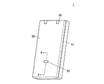
図1は本発明の端末装置の実施形態として、折り畳みタイプの携帯電話機1を示す斜視図である。携帯電話機1は、操作部筐体10と、表示部筐体20と、これらを接続するヒンジ部30とから概略構成される。なお、図1は、操作部筐体10と表示部筐体20とが重ね合わせられた「クローズスタイル」の状態である。「クローズスタイル」においては、図示しないが、操作部筐体10の内側面に設けられたキーパッド等の操作部と、表示部筐体20の前側面に設けられた表示部21(図2参照)とが対向配置されている。
FIG. 1 is a perspective view showing a foldable
図2は図1のII−II切断線における表示部筐体20の断面図である。図2に示すように、表示部筐体20は、ディスプレイパネル23を嵌め込んだ前側ケースと、表示装置24(電子部品)と、インサート板金40(基板)と、フレキシブル基板50と、後側ケース60とを備える。
FIG. 2 is a cross-sectional view of the
ディスプレイパネル23は、ガラスやプラスティックなどの透明部材で構成され、表示部筐体20内の表示装置24を前側面から視認可能としている。表示装置24は携帯電話機1の操作に用いられる画像、文字等の表示に用いられる。表示装置24の上端部にはフレキシブル基板50が接続されている。
The
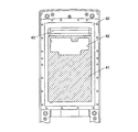
インサート板金40は前側ケースに接続されていて、表示部筐体20の強度を保つ役割を果たす。図3は、ディスプレイパネル23及び表示装置24を外した状態における図2のIII矢視方向から見たインサート板金40及び前側ケースの正面図である。図3に示すように、インサート板金40の前側面には、弾性体からなる緩衝材41が設けられている。緩衝材41の一部には、切り欠き42が設けられている。インサート板金40の背面には、この切り欠き42と対応する位置に、フレキシブル基板50に設けられた光源51や回路素子52、後側ケース60に設けられた光透過部材62等の部品が配置される。
The
インサート板金40の上部には、開口43が設けられている。図2に示すように、この開口43にはフレキシブル基板50が挿通される。
フレキシブル基板50はインサート板金40の後側に配置され、一部がインサート板金40の開口43に挿通されインサート板金40の前側で表示装置24と接続されている。
An
The
フレキシブル基板50の後側面には、光透過部材62と対応する位置にEL素子等の光源51が設けられるとともに、光源51を駆動する回路素子52が設けられている。光源51から放射された光は、光透過部材62を透過して表示部筐体20の後側面に放射される。光源51の光は着信やメール受信等の報知に用いられる。
On the rear side surface of the
後側ケース60には、貫通孔61が設けられており、貫通孔61には光透過部材62が貫通している。光透過部材62は光源51の光を透過させる。
The
光源51及び光透過部材62や、回路素子52が設けられる位置においては、ディスプレイパネル23、表示装置24、インサート板金40、フレキシブル基板50、及び後側ケース60が重ねられている。緩衝材41に切り欠き42がない場合(図4)には、緩衝材41の緩衝能力を超える圧力が表示部筐体20の厚み方向にかかったときに、緩衝材41が硬化してしまい、表示装置24や光源51、回路素子52に圧力が直接及んでしまう。
At the position where the
本実施形態においては、図2に示すように、緩衝材41に切り欠き42が設けられているため、光源51及び光透過部材62や回路素子52の部分に圧力が加わっても、インサート板金40が切り欠き42部分で撓んで衝撃を吸収することができる。したがって、表示装置24や光源51、回路素子52に加わる圧力を低減することができる。また、切り欠き42によりインサート板金40が変形するのに必要なクリアランスを設けることができるので、圧力に対する強度を確保しつつ、表示部筐体20の厚さを薄くすることができる。
In the present embodiment, as shown in FIG. 2, since the
また、インサート板金40に開口43を設け、開口43にフレキシブル基板50を挿通させることで、フレキシブル基板50がインサート板金40に固定されるので、余分な部品を使用せずにフレキシブル基板50を固定することができる。このため、表示部筐体20をさらに薄型化することができる。
Moreover, since the
なお、上記実施形態においては、表示部筐体20について説明したが、本発明は表示部筐体20に限らず、操作部筐体10に適用してもよい。
また、上記実施形態においては、インサート板金40の後側面にフレキシブル基板50を配置した場合について説明したが、本発明はフレキシブル基板50に限らず、通常の回路基板を配置してもよい。
In addition, in the said embodiment, although the display part housing |
Moreover, in the said embodiment, although the case where the
また、本発明の端末装置は携帯電話機に限られず、例えば、パーソナルコンピュータ、電子カメラ、電子腕時計、音楽再生機などの端末装置であってもよい。 Further, the terminal device of the present invention is not limited to a mobile phone, and may be a terminal device such as a personal computer, an electronic camera, an electronic wristwatch, or a music player.
1 携帯電話機(端末装置)
23 ディスプレイパネル
24 表示装置(電子部品)
30 ヒンジ部
40 インサート板金(基板)
41 緩衝材
42 切り欠き
43 開口
50 フレキシブル基板
51 光源
52 回路素子
60 後側ケース
61 貫通孔
62 光透過部材(部品)
1 Mobile phone (terminal equipment)
23
30
41
Claims (7)
前記基板の一方の面に配置された部品と、
前記基板の他方の面に配置された緩衝材と、
これらを内蔵する筐体とを備え、
前記緩衝材には、前記部品の位置と対応する位置に切り欠きが設けられており、
前記切り欠きは、前記緩衝材における前記切り欠き以外の部分に囲まれるように前記緩衝材に設けられている、
ことを特徴とする端末装置。 A substrate,
Components disposed on one side of the substrate;
A cushioning material disposed on the other surface of the substrate;
With a housing containing these,
The buffer material is provided with a notch at a position corresponding to the position of the component ,
The notch is provided in the cushioning material so as to be surrounded by a portion other than the notch in the cushioning material,
A terminal device characterized by that.
前記基板の一方の面に配置されたフレキシブル基板と、
前記フレキシブル基板に搭載された回路素子と、
前記基板の他方の面に配置された緩衝材と、
これらを内蔵する筐体とを備え、
前記緩衝材には、前記回路素子の位置と対応する位置に切り欠きが設けられており、
前記切り欠きは、前記緩衝材における前記切り欠き以外の部分に囲まれるように前記緩衝材に設けられている、
ことを特徴とする端末装置。 A substrate,
A flexible substrate disposed on one side of the substrate;
A circuit element mounted on the flexible substrate;
A cushioning material disposed on the other surface of the substrate;
With a housing containing these,
The buffer material is provided with a notch at a position corresponding to the position of the circuit element ,
The notch is provided in the cushioning material so as to be surrounded by a portion other than the notch in the cushioning material,
A terminal device characterized by that.
前記フレキシブル基板は前記開口を挿通して前記基板の一方の面に設けられた電子部品と接続されることを特徴とする請求項2に記載の端末装置。 The substrate is provided with an opening through which the flexible substrate can be inserted,
The terminal device according to claim 2, wherein the flexible substrate is inserted into the opening and connected to an electronic component provided on one surface of the substrate.
ことを特徴とする請求項1乃至3のいずれか1項に記載の端末装置。 The cushioning material is disposed only on the other surface of the substrate,
Terminal device according to any one of claims 1 to 3, characterized in that.
ことを特徴とする請求項1乃至4のいずれか1項に記載の端末装置。 The cushioning material is smaller than the substrate,
Terminal device according to any one of claims 1 to 4, characterized in that.
ことを特徴とする請求項1乃至5のいずれか1項に記載の端末装置。 The cushioning material has a single-sheet structure,
Terminal device according to any one of claims 1 to 5, characterized in that.
前記緩衝材は、前記表示装置と前記基板との間に配置されている、
ことを特徴とする請求項1乃至6のいずれか1項に記載の端末装置。 A display device,
The cushioning material is disposed between the display device and the substrate.
Terminal device according to any one of claims 1 to 6, characterized in that.
Priority Applications (1)
| Application Number | Priority Date | Filing Date | Title |
|---|---|---|---|
| JP2007289751A JP4985331B2 (en) | 2007-11-07 | 2007-11-07 | Terminal device |
Applications Claiming Priority (1)
| Application Number | Priority Date | Filing Date | Title |
|---|---|---|---|
| JP2007289751A JP4985331B2 (en) | 2007-11-07 | 2007-11-07 | Terminal device |
Publications (2)
| Publication Number | Publication Date |
|---|---|
| JP2009118243A JP2009118243A (en) | 2009-05-28 |
| JP4985331B2 true JP4985331B2 (en) | 2012-07-25 |
Family
ID=40784862
Family Applications (1)
| Application Number | Title | Priority Date | Filing Date |
|---|---|---|---|
| JP2007289751A Expired - Fee Related JP4985331B2 (en) | 2007-11-07 | 2007-11-07 | Terminal device |
Country Status (1)
| Country | Link |
|---|---|
| JP (1) | JP4985331B2 (en) |
Family Cites Families (3)
| Publication number | Priority date | Publication date | Assignee | Title |
|---|---|---|---|---|
| JP2001007550A (en) * | 1999-06-24 | 2001-01-12 | Nec Corp | Portable information radio terminal device and its manufacture |
| JP4468061B2 (en) * | 2004-04-30 | 2010-05-26 | 株式会社 日立ディスプレイズ | Display device |
| JP4460500B2 (en) * | 2005-07-28 | 2010-05-12 | 京セラ株式会社 | Mobile terminal device |
-
2007
- 2007-11-07 JP JP2007289751A patent/JP4985331B2/en not_active Expired - Fee Related
Also Published As
| Publication number | Publication date |
|---|---|
| JP2009118243A (en) | 2009-05-28 |
Similar Documents
| Publication | Publication Date | Title |
|---|---|---|
| US8265716B2 (en) | Mobile terminal device | |
| JP4385252B2 (en) | Dust-proof structure for LCD in electronic device and electronic device having the structure | |
| JP2007025695A (en) | Display module and portable terminal equipped with the same | |
| JP4777320B2 (en) | Electronics | |
| JP2005189512A (en) | Impact absorption structure of rear lcd in electronic device and electronic device provided with the structure | |
| JP4405532B2 (en) | Foldable mobile phone | |
| JP5489475B2 (en) | Portable electronic devices | |
| JP4985331B2 (en) | Terminal device | |
| WO2011145259A1 (en) | Portable apparatus | |
| CN101753652A (en) | Mobile terminal apparatus | |
| JP5398042B2 (en) | Sound emission structure of housing and electronic device | |
| JP5063186B2 (en) | Mobile terminal device | |
| JP2006135842A (en) | Portable electronic devices | |
| JP4182067B2 (en) | Foldable electronic device and case abutting structure of foldable electronic device | |
| JP2007033658A (en) | Information processing device | |
| JP5234805B2 (en) | Sound emission structure of housing and electronic device | |
| JP2010277750A (en) | Portable electronic devices | |
| JP4994114B2 (en) | Mobile terminal device | |
| JP4912898B2 (en) | Display device | |
| JP2009100139A (en) | Portable electronic devices | |
| JP2006139538A (en) | Electronics | |
| JP2014090184A (en) | Electronic component housing structure, and electronic apparatus | |
| JP2005210419A (en) | Portable device | |
| JP4659639B2 (en) | Mobile device | |
| JP2009111598A (en) | Foldable electronics |
Legal Events
| Date | Code | Title | Description |
|---|---|---|---|
| A621 | Written request for application examination |
Free format text: JAPANESE INTERMEDIATE CODE: A621 Effective date: 20100217 |
|
| RD01 | Notification of change of attorney |
Free format text: JAPANESE INTERMEDIATE CODE: A7421 Effective date: 20100309 |
|
| A711 | Notification of change in applicant |
Free format text: JAPANESE INTERMEDIATE CODE: A712 Effective date: 20100805 |
|
| A977 | Report on retrieval |
Free format text: JAPANESE INTERMEDIATE CODE: A971007 Effective date: 20110425 |
|
| A131 | Notification of reasons for refusal |
Free format text: JAPANESE INTERMEDIATE CODE: A131 Effective date: 20110510 |
|
| A521 | Written amendment |
Free format text: JAPANESE INTERMEDIATE CODE: A523 Effective date: 20110705 |
|
| A02 | Decision of refusal |
Free format text: JAPANESE INTERMEDIATE CODE: A02 Effective date: 20111108 |
|
| A521 | Written amendment |
Free format text: JAPANESE INTERMEDIATE CODE: A523 Effective date: 20120207 |
|
| A911 | Transfer of reconsideration by examiner before appeal (zenchi) |
Free format text: JAPANESE INTERMEDIATE CODE: A911 Effective date: 20120214 |
|
| TRDD | Decision of grant or rejection written | ||
| A01 | Written decision to grant a patent or to grant a registration (utility model) |
Free format text: JAPANESE INTERMEDIATE CODE: A01 Effective date: 20120403 |
|
| A01 | Written decision to grant a patent or to grant a registration (utility model) |
Free format text: JAPANESE INTERMEDIATE CODE: A01 |
|
| A61 | First payment of annual fees (during grant procedure) |
Free format text: JAPANESE INTERMEDIATE CODE: A61 Effective date: 20120416 |
|
| R150 | Certificate of patent or registration of utility model |
Free format text: JAPANESE INTERMEDIATE CODE: R150 |
|
| FPAY | Renewal fee payment (event date is renewal date of database) |
Free format text: PAYMENT UNTIL: 20150511 Year of fee payment: 3 |
|
| FPAY | Renewal fee payment (event date is renewal date of database) |
Free format text: PAYMENT UNTIL: 20150511 Year of fee payment: 3 |
|
| S111 | Request for change of ownership or part of ownership |
Free format text: JAPANESE INTERMEDIATE CODE: R313113 |
|
| FPAY | Renewal fee payment (event date is renewal date of database) |
Free format text: PAYMENT UNTIL: 20150511 Year of fee payment: 3 |
|
| R350 | Written notification of registration of transfer |
Free format text: JAPANESE INTERMEDIATE CODE: R350 |
|
| S111 | Request for change of ownership or part of ownership |
Free format text: JAPANESE INTERMEDIATE CODE: R313113 |
|
| R350 | Written notification of registration of transfer |
Free format text: JAPANESE INTERMEDIATE CODE: R350 |
|
| LAPS | Cancellation because of no payment of annual fees |