EP2422842B1 - Verpackung für eine implantierbare Nervenstimulationsvorrichtung - Google Patents
Verpackung für eine implantierbare Nervenstimulationsvorrichtung Download PDFInfo
- Publication number
- EP2422842B1 EP2422842B1 EP11185514.4A EP11185514A EP2422842B1 EP 2422842 B1 EP2422842 B1 EP 2422842B1 EP 11185514 A EP11185514 A EP 11185514A EP 2422842 B1 EP2422842 B1 EP 2422842B1
- Authority
- EP
- European Patent Office
- Prior art keywords
- implantable device
- substrate
- conductive
- metal traces
- package
- Prior art date
- Legal status (The legal status is an assumption and is not a legal conclusion. Google has not performed a legal analysis and makes no representation as to the accuracy of the status listed.)
- Active
Links
- 230000000638 stimulation Effects 0.000 title description 18
- 230000001537 neural effect Effects 0.000 title description 11
- 239000000758 substrate Substances 0.000 claims description 64
- 239000000919 ceramic Substances 0.000 claims description 36
- 229910052751 metal Inorganic materials 0.000 claims description 34
- 239000002184 metal Substances 0.000 claims description 34
- BASFCYQUMIYNBI-UHFFFAOYSA-N platinum Chemical compound [Pt] BASFCYQUMIYNBI-UHFFFAOYSA-N 0.000 claims description 26
- 239000010410 layer Substances 0.000 claims description 22
- KDLHZDBZIXYQEI-UHFFFAOYSA-N Palladium Chemical compound [Pd] KDLHZDBZIXYQEI-UHFFFAOYSA-N 0.000 claims description 16
- 229910052697 platinum Inorganic materials 0.000 claims description 14
- PCHJSUWPFVWCPO-UHFFFAOYSA-N gold Chemical compound [Au] PCHJSUWPFVWCPO-UHFFFAOYSA-N 0.000 claims description 11
- 229910052737 gold Inorganic materials 0.000 claims description 11
- 239000010931 gold Substances 0.000 claims description 11
- 229910052719 titanium Inorganic materials 0.000 claims description 9
- 239000010936 titanium Substances 0.000 claims description 9
- 239000004593 Epoxy Substances 0.000 claims description 8
- 150000002739 metals Chemical class 0.000 claims description 8
- 229910052763 palladium Inorganic materials 0.000 claims description 8
- RTAQQCXQSZGOHL-UHFFFAOYSA-N Titanium Chemical compound [Ti] RTAQQCXQSZGOHL-UHFFFAOYSA-N 0.000 claims description 7
- 229910045601 alloy Inorganic materials 0.000 claims description 5
- 239000000956 alloy Substances 0.000 claims description 5
- 229910052741 iridium Inorganic materials 0.000 claims description 5
- 239000004642 Polyimide Substances 0.000 claims description 4
- 239000000203 mixture Substances 0.000 claims description 4
- 229920001721 polyimide Polymers 0.000 claims description 4
- 229910052709 silver Inorganic materials 0.000 claims description 4
- 229910001260 Pt alloy Inorganic materials 0.000 claims description 3
- GKOZUEZYRPOHIO-UHFFFAOYSA-N iridium atom Chemical compound [Ir] GKOZUEZYRPOHIO-UHFFFAOYSA-N 0.000 claims description 3
- BQCADISMDOOEFD-UHFFFAOYSA-N Silver Chemical compound [Ag] BQCADISMDOOEFD-UHFFFAOYSA-N 0.000 claims description 2
- 229910001069 Ti alloy Inorganic materials 0.000 claims description 2
- 229910001092 metal group alloy Inorganic materials 0.000 claims description 2
- 239000004332 silver Substances 0.000 claims description 2
- 230000004936 stimulating effect Effects 0.000 claims description 2
- 229910052715 tantalum Inorganic materials 0.000 claims description 2
- GUVRBAGPIYLISA-UHFFFAOYSA-N tantalum atom Chemical compound [Ta] GUVRBAGPIYLISA-UHFFFAOYSA-N 0.000 claims description 2
- 229910000575 Ir alloy Inorganic materials 0.000 claims 1
- 229920001940 conductive polymer Polymers 0.000 claims 1
- 239000000428 dust Substances 0.000 claims 1
- 239000000843 powder Substances 0.000 claims 1
- 230000001939 inductive effect Effects 0.000 description 28
- 230000002207 retinal effect Effects 0.000 description 26
- 210000001525 retina Anatomy 0.000 description 16
- 210000003786 sclera Anatomy 0.000 description 16
- 229920000642 polymer Polymers 0.000 description 10
- 238000001465 metallisation Methods 0.000 description 9
- 239000000463 material Substances 0.000 description 8
- 229920001296 polysiloxane Polymers 0.000 description 8
- 239000010409 thin film Substances 0.000 description 8
- 230000000007 visual effect Effects 0.000 description 8
- 238000002513 implantation Methods 0.000 description 7
- 238000000034 method Methods 0.000 description 7
- 206010034962 Photopsia Diseases 0.000 description 6
- 210000000795 conjunctiva Anatomy 0.000 description 6
- 239000007943 implant Substances 0.000 description 6
- 229910000065 phosphene Inorganic materials 0.000 description 6
- 238000011084 recovery Methods 0.000 description 6
- 210000001519 tissue Anatomy 0.000 description 6
- 230000001976 improved effect Effects 0.000 description 5
- 210000003205 muscle Anatomy 0.000 description 5
- MCMNRKCIXSYSNV-UHFFFAOYSA-N Zirconium dioxide Chemical compound O=[Zr]=O MCMNRKCIXSYSNV-UHFFFAOYSA-N 0.000 description 4
- 210000004027 cell Anatomy 0.000 description 4
- 230000008569 process Effects 0.000 description 4
- 210000003161 choroid Anatomy 0.000 description 3
- 238000002474 experimental method Methods 0.000 description 3
- 230000004438 eyesight Effects 0.000 description 3
- 230000035876 healing Effects 0.000 description 3
- 230000001771 impaired effect Effects 0.000 description 3
- 210000000653 nervous system Anatomy 0.000 description 3
- 210000002569 neuron Anatomy 0.000 description 3
- 229910052707 ruthenium Inorganic materials 0.000 description 3
- 238000003466 welding Methods 0.000 description 3
- 201000004569 Blindness Diseases 0.000 description 2
- 241000282326 Felis catus Species 0.000 description 2
- 229920000544 Gore-Tex Polymers 0.000 description 2
- 239000000853 adhesive Substances 0.000 description 2
- 230000001070 adhesive effect Effects 0.000 description 2
- PNEYBMLMFCGWSK-UHFFFAOYSA-N aluminium oxide Inorganic materials [O-2].[O-2].[O-2].[Al+3].[Al+3] PNEYBMLMFCGWSK-UHFFFAOYSA-N 0.000 description 2
- 239000011230 binding agent Substances 0.000 description 2
- 239000003990 capacitor Substances 0.000 description 2
- 239000011248 coating agent Substances 0.000 description 2
- 238000000576 coating method Methods 0.000 description 2
- 230000006835 compression Effects 0.000 description 2
- 238000007906 compression Methods 0.000 description 2
- 239000004020 conductor Substances 0.000 description 2
- 239000010949 copper Substances 0.000 description 2
- 229910052802 copper Inorganic materials 0.000 description 2
- 230000001054 cortical effect Effects 0.000 description 2
- 230000003628 erosive effect Effects 0.000 description 2
- 239000010408 film Substances 0.000 description 2
- 229910052742 iron Inorganic materials 0.000 description 2
- 210000005036 nerve Anatomy 0.000 description 2
- 229910052759 nickel Inorganic materials 0.000 description 2
- PXHVJJICTQNCMI-UHFFFAOYSA-N nickel Substances [Ni] PXHVJJICTQNCMI-UHFFFAOYSA-N 0.000 description 2
- NJPPVKZQTLUDBO-UHFFFAOYSA-N novaluron Chemical compound C1=C(Cl)C(OC(F)(F)C(OC(F)(F)F)F)=CC=C1NC(=O)NC(=O)C1=C(F)C=CC=C1F NJPPVKZQTLUDBO-UHFFFAOYSA-N 0.000 description 2
- 108091008695 photoreceptors Proteins 0.000 description 2
- 229920000728 polyester Polymers 0.000 description 2
- 229920001343 polytetrafluoroethylene Polymers 0.000 description 2
- 239000011148 porous material Substances 0.000 description 2
- 230000001681 protective effect Effects 0.000 description 2
- 229910052703 rhodium Inorganic materials 0.000 description 2
- 238000007493 shaping process Methods 0.000 description 2
- 229920002379 silicone rubber Polymers 0.000 description 2
- 239000010944 silver (metal) Substances 0.000 description 2
- 238000001356 surgical procedure Methods 0.000 description 2
- 229910052726 zirconium Inorganic materials 0.000 description 2
- 229910001020 Au alloy Inorganic materials 0.000 description 1
- 208000002177 Cataract Diseases 0.000 description 1
- 102000008186 Collagen Human genes 0.000 description 1
- 108010035532 Collagen Proteins 0.000 description 1
- 229920004934 Dacron® Polymers 0.000 description 1
- 208000027534 Emotional disease Diseases 0.000 description 1
- 208000003098 Ganglion Cysts Diseases 0.000 description 1
- 229910001252 Pd alloy Chemical group 0.000 description 1
- XYFCBTPGUUZFHI-UHFFFAOYSA-N Phosphine Chemical compound P XYFCBTPGUUZFHI-UHFFFAOYSA-N 0.000 description 1
- 208000017442 Retinal disease Diseases 0.000 description 1
- 208000007014 Retinitis pigmentosa Diseases 0.000 description 1
- KJTLSVCANCCWHF-UHFFFAOYSA-N Ruthenium Chemical compound [Ru] KJTLSVCANCCWHF-UHFFFAOYSA-N 0.000 description 1
- 208000005400 Synovial Cyst Diseases 0.000 description 1
- 239000004809 Teflon Substances 0.000 description 1
- 229920006362 Teflon® Polymers 0.000 description 1
- 230000002745 absorbent Effects 0.000 description 1
- 239000002250 absorbent Substances 0.000 description 1
- 230000036982 action potential Effects 0.000 description 1
- 210000000577 adipose tissue Anatomy 0.000 description 1
- 206010064930 age-related macular degeneration Diseases 0.000 description 1
- 230000000712 assembly Effects 0.000 description 1
- 238000000429 assembly Methods 0.000 description 1
- 230000009286 beneficial effect Effects 0.000 description 1
- 229920001400 block copolymer Polymers 0.000 description 1
- 230000036770 blood supply Effects 0.000 description 1
- 238000005219 brazing Methods 0.000 description 1
- 210000004720 cerebrum Anatomy 0.000 description 1
- 229920001436 collagen Polymers 0.000 description 1
- 229920001577 copolymer Polymers 0.000 description 1
- 230000007797 corrosion Effects 0.000 description 1
- 238000005260 corrosion Methods 0.000 description 1
- 210000005257 cortical tissue Anatomy 0.000 description 1
- 230000001186 cumulative effect Effects 0.000 description 1
- 230000003412 degenerative effect Effects 0.000 description 1
- 238000013461 design Methods 0.000 description 1
- 238000009826 distribution Methods 0.000 description 1
- 230000000694 effects Effects 0.000 description 1
- 238000005516 engineering process Methods 0.000 description 1
- 229920000295 expanded polytetrafluoroethylene Polymers 0.000 description 1
- 230000004424 eye movement Effects 0.000 description 1
- 210000000744 eyelid Anatomy 0.000 description 1
- 238000010304 firing Methods 0.000 description 1
- 239000011521 glass Substances 0.000 description 1
- QUCZBHXJAUTYHE-UHFFFAOYSA-N gold Chemical compound [Au].[Au] QUCZBHXJAUTYHE-UHFFFAOYSA-N 0.000 description 1
- 239000003353 gold alloy Substances 0.000 description 1
- 210000003128 head Anatomy 0.000 description 1
- 208000015181 infectious disease Diseases 0.000 description 1
- 230000003993 interaction Effects 0.000 description 1
- 230000007794 irritation Effects 0.000 description 1
- 208000002780 macular degeneration Diseases 0.000 description 1
- 238000004519 manufacturing process Methods 0.000 description 1
- 239000011159 matrix material Substances 0.000 description 1
- 230000007246 mechanism Effects 0.000 description 1
- 239000012528 membrane Substances 0.000 description 1
- 238000012986 modification Methods 0.000 description 1
- 230000004048 modification Effects 0.000 description 1
- 229910001000 nickel titanium Inorganic materials 0.000 description 1
- 229910052758 niobium Inorganic materials 0.000 description 1
- 239000010955 niobium Substances 0.000 description 1
- GUCVJGMIXFAOAE-UHFFFAOYSA-N niobium atom Chemical compound [Nb] GUCVJGMIXFAOAE-UHFFFAOYSA-N 0.000 description 1
- 239000011295 pitch Substances 0.000 description 1
- 229920000052 poly(p-xylylene) Polymers 0.000 description 1
- 239000005020 polyethylene terephthalate Substances 0.000 description 1
- 229920002959 polymer blend Polymers 0.000 description 1
- 239000004810 polytetrafluoroethylene Substances 0.000 description 1
- 230000001737 promoting effect Effects 0.000 description 1
- 210000003994 retinal ganglion cell Anatomy 0.000 description 1
- 210000001116 retinal neuron Anatomy 0.000 description 1
- 229910001925 ruthenium oxide Inorganic materials 0.000 description 1
- WOCIAKWEIIZHES-UHFFFAOYSA-N ruthenium(iv) oxide Chemical compound O=[Ru]=O WOCIAKWEIIZHES-UHFFFAOYSA-N 0.000 description 1
- 238000007789 sealing Methods 0.000 description 1
- 230000035807 sensation Effects 0.000 description 1
- 230000001953 sensory effect Effects 0.000 description 1
- 238000007920 subcutaneous administration Methods 0.000 description 1
- 238000012546 transfer Methods 0.000 description 1
- 230000016776 visual perception Effects 0.000 description 1
- 239000003039 volatile agent Substances 0.000 description 1
Images


Classifications
-
- A—HUMAN NECESSITIES
- A61—MEDICAL OR VETERINARY SCIENCE; HYGIENE
- A61N—ELECTROTHERAPY; MAGNETOTHERAPY; RADIATION THERAPY; ULTRASOUND THERAPY
- A61N1/00—Electrotherapy; Circuits therefor
- A61N1/18—Applying electric currents by contact electrodes
- A61N1/32—Applying electric currents by contact electrodes alternating or intermittent currents
- A61N1/36—Applying electric currents by contact electrodes alternating or intermittent currents for stimulation
- A61N1/36046—Applying electric currents by contact electrodes alternating or intermittent currents for stimulation of the eye
-
- A—HUMAN NECESSITIES
- A61—MEDICAL OR VETERINARY SCIENCE; HYGIENE
- A61F—FILTERS IMPLANTABLE INTO BLOOD VESSELS; PROSTHESES; DEVICES PROVIDING PATENCY TO, OR PREVENTING COLLAPSING OF, TUBULAR STRUCTURES OF THE BODY, e.g. STENTS; ORTHOPAEDIC, NURSING OR CONTRACEPTIVE DEVICES; FOMENTATION; TREATMENT OR PROTECTION OF EYES OR EARS; BANDAGES, DRESSINGS OR ABSORBENT PADS; FIRST-AID KITS
- A61F15/00—Auxiliary appliances for wound dressings; Dispensing containers for dressings or bandages
- A61F15/001—Packages or dispensers for bandages, cotton balls, drapes, dressings, gauze, gowns, sheets, sponges, swabsticks or towels
-
- A—HUMAN NECESSITIES
- A61—MEDICAL OR VETERINARY SCIENCE; HYGIENE
- A61N—ELECTROTHERAPY; MAGNETOTHERAPY; RADIATION THERAPY; ULTRASOUND THERAPY
- A61N1/00—Electrotherapy; Circuits therefor
- A61N1/02—Details
- A61N1/04—Electrodes
- A61N1/05—Electrodes for implantation or insertion into the body, e.g. heart electrode
- A61N1/0526—Head electrodes
- A61N1/0543—Retinal electrodes
-
- A—HUMAN NECESSITIES
- A61—MEDICAL OR VETERINARY SCIENCE; HYGIENE
- A61N—ELECTROTHERAPY; MAGNETOTHERAPY; RADIATION THERAPY; ULTRASOUND THERAPY
- A61N1/00—Electrotherapy; Circuits therefor
- A61N1/18—Applying electric currents by contact electrodes
- A61N1/32—Applying electric currents by contact electrodes alternating or intermittent currents
- A61N1/36—Applying electric currents by contact electrodes alternating or intermittent currents for stimulation
- A61N1/3605—Implantable neurostimulators for stimulating central or peripheral nerve system
- A61N1/36125—Details of circuitry or electric components
-
- A—HUMAN NECESSITIES
- A61—MEDICAL OR VETERINARY SCIENCE; HYGIENE
- A61N—ELECTROTHERAPY; MAGNETOTHERAPY; RADIATION THERAPY; ULTRASOUND THERAPY
- A61N1/00—Electrotherapy; Circuits therefor
- A61N1/18—Applying electric currents by contact electrodes
- A61N1/32—Applying electric currents by contact electrodes alternating or intermittent currents
- A61N1/36—Applying electric currents by contact electrodes alternating or intermittent currents for stimulation
- A61N1/372—Arrangements in connection with the implantation of stimulators
- A61N1/375—Constructional arrangements, e.g. casings
- A61N1/37518—Anchoring of the implants, e.g. fixation
-
- H—ELECTRICITY
- H01—ELECTRIC ELEMENTS
- H01L—SEMICONDUCTOR DEVICES NOT COVERED BY CLASS H10
- H01L23/00—Details of semiconductor or other solid state devices
- H01L23/02—Containers; Seals
- H01L23/04—Containers; Seals characterised by the shape of the container or parts, e.g. caps, walls
- H01L23/053—Containers; Seals characterised by the shape of the container or parts, e.g. caps, walls the container being a hollow construction and having an insulating or insulated base as a mounting for the semiconductor body
- H01L23/055—Containers; Seals characterised by the shape of the container or parts, e.g. caps, walls the container being a hollow construction and having an insulating or insulated base as a mounting for the semiconductor body the leads having a passage through the base
-
- H—ELECTRICITY
- H01—ELECTRIC ELEMENTS
- H01L—SEMICONDUCTOR DEVICES NOT COVERED BY CLASS H10
- H01L23/00—Details of semiconductor or other solid state devices
- H01L23/02—Containers; Seals
- H01L23/06—Containers; Seals characterised by the material of the container or its electrical properties
-
- H—ELECTRICITY
- H01—ELECTRIC ELEMENTS
- H01L—SEMICONDUCTOR DEVICES NOT COVERED BY CLASS H10
- H01L23/00—Details of semiconductor or other solid state devices
- H01L23/02—Containers; Seals
- H01L23/06—Containers; Seals characterised by the material of the container or its electrical properties
- H01L23/08—Containers; Seals characterised by the material of the container or its electrical properties the material being an electrical insulator, e.g. glass
-
- H—ELECTRICITY
- H01—ELECTRIC ELEMENTS
- H01L—SEMICONDUCTOR DEVICES NOT COVERED BY CLASS H10
- H01L23/00—Details of semiconductor or other solid state devices
- H01L23/02—Containers; Seals
- H01L23/10—Containers; Seals characterised by the material or arrangement of seals between parts, e.g. between cap and base of the container or between leads and walls of the container
-
- H—ELECTRICITY
- H01—ELECTRIC ELEMENTS
- H01L—SEMICONDUCTOR DEVICES NOT COVERED BY CLASS H10
- H01L24/00—Arrangements for connecting or disconnecting semiconductor or solid-state bodies; Methods or apparatus related thereto
- H01L24/01—Means for bonding being attached to, or being formed on, the surface to be connected, e.g. chip-to-package, die-attach, "first-level" interconnects; Manufacturing methods related thereto
- H01L24/10—Bump connectors ; Manufacturing methods related thereto
- H01L24/15—Structure, shape, material or disposition of the bump connectors after the connecting process
- H01L24/16—Structure, shape, material or disposition of the bump connectors after the connecting process of an individual bump connector
-
- H—ELECTRICITY
- H01—ELECTRIC ELEMENTS
- H01L—SEMICONDUCTOR DEVICES NOT COVERED BY CLASS H10
- H01L25/00—Assemblies consisting of a plurality of individual semiconductor or other solid state devices ; Multistep manufacturing processes thereof
- H01L25/18—Assemblies consisting of a plurality of individual semiconductor or other solid state devices ; Multistep manufacturing processes thereof the devices being of types provided for in two or more different subgroups of the same main group of groups H01L27/00 - H01L33/00, or in a single subclass of H10K, H10N
-
- A—HUMAN NECESSITIES
- A61—MEDICAL OR VETERINARY SCIENCE; HYGIENE
- A61N—ELECTROTHERAPY; MAGNETOTHERAPY; RADIATION THERAPY; ULTRASOUND THERAPY
- A61N1/00—Electrotherapy; Circuits therefor
- A61N1/02—Details
- A61N1/04—Electrodes
- A61N1/05—Electrodes for implantation or insertion into the body, e.g. heart electrode
- A61N1/0526—Head electrodes
- A61N1/0529—Electrodes for brain stimulation
-
- H—ELECTRICITY
- H01—ELECTRIC ELEMENTS
- H01L—SEMICONDUCTOR DEVICES NOT COVERED BY CLASS H10
- H01L2224/00—Indexing scheme for arrangements for connecting or disconnecting semiconductor or solid-state bodies and methods related thereto as covered by H01L24/00
- H01L2224/01—Means for bonding being attached to, or being formed on, the surface to be connected, e.g. chip-to-package, die-attach, "first-level" interconnects; Manufacturing methods related thereto
- H01L2224/10—Bump connectors; Manufacturing methods related thereto
- H01L2224/15—Structure, shape, material or disposition of the bump connectors after the connecting process
- H01L2224/16—Structure, shape, material or disposition of the bump connectors after the connecting process of an individual bump connector
- H01L2224/161—Disposition
- H01L2224/16151—Disposition the bump connector connecting between a semiconductor or solid-state body and an item not being a semiconductor or solid-state body, e.g. chip-to-substrate, chip-to-passive
- H01L2224/16221—Disposition the bump connector connecting between a semiconductor or solid-state body and an item not being a semiconductor or solid-state body, e.g. chip-to-substrate, chip-to-passive the body and the item being stacked
- H01L2224/16225—Disposition the bump connector connecting between a semiconductor or solid-state body and an item not being a semiconductor or solid-state body, e.g. chip-to-substrate, chip-to-passive the body and the item being stacked the item being non-metallic, e.g. insulating substrate with or without metallisation
-
- H—ELECTRICITY
- H01—ELECTRIC ELEMENTS
- H01L—SEMICONDUCTOR DEVICES NOT COVERED BY CLASS H10
- H01L2224/00—Indexing scheme for arrangements for connecting or disconnecting semiconductor or solid-state bodies and methods related thereto as covered by H01L24/00
- H01L2224/01—Means for bonding being attached to, or being formed on, the surface to be connected, e.g. chip-to-package, die-attach, "first-level" interconnects; Manufacturing methods related thereto
- H01L2224/42—Wire connectors; Manufacturing methods related thereto
- H01L2224/44—Structure, shape, material or disposition of the wire connectors prior to the connecting process
- H01L2224/45—Structure, shape, material or disposition of the wire connectors prior to the connecting process of an individual wire connector
- H01L2224/45001—Core members of the connector
- H01L2224/45099—Material
- H01L2224/451—Material with a principal constituent of the material being a metal or a metalloid, e.g. boron (B), silicon (Si), germanium (Ge), arsenic (As), antimony (Sb), tellurium (Te) and polonium (Po), and alloys thereof
- H01L2224/45138—Material with a principal constituent of the material being a metal or a metalloid, e.g. boron (B), silicon (Si), germanium (Ge), arsenic (As), antimony (Sb), tellurium (Te) and polonium (Po), and alloys thereof the principal constituent melting at a temperature of greater than or equal to 950°C and less than 1550°C
- H01L2224/45144—Gold (Au) as principal constituent
-
- H—ELECTRICITY
- H01—ELECTRIC ELEMENTS
- H01L—SEMICONDUCTOR DEVICES NOT COVERED BY CLASS H10
- H01L2224/00—Indexing scheme for arrangements for connecting or disconnecting semiconductor or solid-state bodies and methods related thereto as covered by H01L24/00
- H01L2224/01—Means for bonding being attached to, or being formed on, the surface to be connected, e.g. chip-to-package, die-attach, "first-level" interconnects; Manufacturing methods related thereto
- H01L2224/42—Wire connectors; Manufacturing methods related thereto
- H01L2224/47—Structure, shape, material or disposition of the wire connectors after the connecting process
- H01L2224/48—Structure, shape, material or disposition of the wire connectors after the connecting process of an individual wire connector
- H01L2224/4805—Shape
- H01L2224/4809—Loop shape
- H01L2224/48091—Arched
-
- H—ELECTRICITY
- H01—ELECTRIC ELEMENTS
- H01L—SEMICONDUCTOR DEVICES NOT COVERED BY CLASS H10
- H01L2224/00—Indexing scheme for arrangements for connecting or disconnecting semiconductor or solid-state bodies and methods related thereto as covered by H01L24/00
- H01L2224/01—Means for bonding being attached to, or being formed on, the surface to be connected, e.g. chip-to-package, die-attach, "first-level" interconnects; Manufacturing methods related thereto
- H01L2224/42—Wire connectors; Manufacturing methods related thereto
- H01L2224/47—Structure, shape, material or disposition of the wire connectors after the connecting process
- H01L2224/48—Structure, shape, material or disposition of the wire connectors after the connecting process of an individual wire connector
- H01L2224/481—Disposition
- H01L2224/48105—Connecting bonding areas at different heights
- H01L2224/48106—Connecting bonding areas at different heights the connector being orthogonal to a side surface of the semiconductor or solid-state body, e.g. parallel layout
-
- H—ELECTRICITY
- H01—ELECTRIC ELEMENTS
- H01L—SEMICONDUCTOR DEVICES NOT COVERED BY CLASS H10
- H01L2224/00—Indexing scheme for arrangements for connecting or disconnecting semiconductor or solid-state bodies and methods related thereto as covered by H01L24/00
- H01L2224/01—Means for bonding being attached to, or being formed on, the surface to be connected, e.g. chip-to-package, die-attach, "first-level" interconnects; Manufacturing methods related thereto
- H01L2224/42—Wire connectors; Manufacturing methods related thereto
- H01L2224/47—Structure, shape, material or disposition of the wire connectors after the connecting process
- H01L2224/48—Structure, shape, material or disposition of the wire connectors after the connecting process of an individual wire connector
- H01L2224/481—Disposition
- H01L2224/48151—Connecting between a semiconductor or solid-state body and an item not being a semiconductor or solid-state body, e.g. chip-to-substrate, chip-to-passive
- H01L2224/48221—Connecting between a semiconductor or solid-state body and an item not being a semiconductor or solid-state body, e.g. chip-to-substrate, chip-to-passive the body and the item being stacked
- H01L2224/48225—Connecting between a semiconductor or solid-state body and an item not being a semiconductor or solid-state body, e.g. chip-to-substrate, chip-to-passive the body and the item being stacked the item being non-metallic, e.g. insulating substrate with or without metallisation
-
- H—ELECTRICITY
- H01—ELECTRIC ELEMENTS
- H01L—SEMICONDUCTOR DEVICES NOT COVERED BY CLASS H10
- H01L24/00—Arrangements for connecting or disconnecting semiconductor or solid-state bodies; Methods or apparatus related thereto
- H01L24/01—Means for bonding being attached to, or being formed on, the surface to be connected, e.g. chip-to-package, die-attach, "first-level" interconnects; Manufacturing methods related thereto
- H01L24/42—Wire connectors; Manufacturing methods related thereto
- H01L24/47—Structure, shape, material or disposition of the wire connectors after the connecting process
- H01L24/48—Structure, shape, material or disposition of the wire connectors after the connecting process of an individual wire connector
-
- H—ELECTRICITY
- H01—ELECTRIC ELEMENTS
- H01L—SEMICONDUCTOR DEVICES NOT COVERED BY CLASS H10
- H01L2924/00—Indexing scheme for arrangements or methods for connecting or disconnecting semiconductor or solid-state bodies as covered by H01L24/00
- H01L2924/0001—Technical content checked by a classifier
- H01L2924/00011—Not relevant to the scope of the group, the symbol of which is combined with the symbol of this group
-
- H—ELECTRICITY
- H01—ELECTRIC ELEMENTS
- H01L—SEMICONDUCTOR DEVICES NOT COVERED BY CLASS H10
- H01L2924/00—Indexing scheme for arrangements or methods for connecting or disconnecting semiconductor or solid-state bodies as covered by H01L24/00
- H01L2924/0001—Technical content checked by a classifier
- H01L2924/00014—Technical content checked by a classifier the subject-matter covered by the group, the symbol of which is combined with the symbol of this group, being disclosed without further technical details
Definitions
- the present invention is generally directed to neural stimulation and more specifically to an improved hermetic package for an implantable neural stimulation device.
- Foerster investigated the effect of electrically stimulating the exposed occipital pole of one cerebral hemisphere. He found that, when a point at the extreme occipital pole was stimulated, the patient perceived a small spot of light directly in front and motionless (a phosphene). Subsequently, Brindley and Lewin (1968) thoroughly studied electrical stimulation of the human occipital (visual) cortex. By varying the stimulation parameters, these investigators described in detail the location of the phosphenes produced relative to the specific region of the occipital cortex stimulated. These experiments demonstrated: (1) the consistent shape and position of phosphenes; (2) that increased stimulation pulse duration made phosphenes brighter; and (3) that there was no detectable interaction between neighboring electrodes which were as close as 2.4 mm apart.
- Neural tissue can be artificially stimulated and activated by prosthetic devices that pass pulses of electrical current through electrodes on such a device.
- the passage of current causes changes in electrical potentials across visual neuronal membranes, which can initiate visual neuron action potentials, which are the means of information transfer in the nervous system.
- neural tissue stimulation is in the rehabilitation of the blind.
- Some forms of blindness involve selective loss of the light sensitive transducers of the retina.
- Other retinal neurons remain viable, however, and may be activated in the manner described above by placement of a prosthetic electrode device on the inner (toward the vitreous) retinal surface (epiretinal). This placement must be mechanically stable, minimize the distance between the device electrodes and the visual neurons, control the electronic field distribution and avoid undue compression of the visual neurons.
- Bullara US Pat. No. 4,573,481 patented an electrode assembly for surgical implantation on a nerve.
- the matrix was silicone with embedded iridium electrodes.
- the assembly fit around a nerve to stimulate it.
- the Michelson '933 apparatus includes an array of photosensitive devices on its surface that are connected to a plurality of electrodes positioned on the opposite surface of the device to stimulate the retina. These electrodes are disposed to form an array similar to a "bed of nails" having conductors which impinge directly on the retina to stimulate the retinal cells.
- US Patent 4,837,049 to Byers describes spike electrodes for neural stimulation. Each spike electrode pierces neural tissue for better electrical contact.
- US Patent 5,215,088 to Norman describes an array of spike electrodes for cortical stimulation. Each spike pierces cortical tissue for better electrical contact.
- retinal tacks info retinas in an effort to reattach retinas that had detached from the underlying choroid, which is the source of blood supply for the outer retina and thus the photoreceptors. See, e.g., E. de Juan, et al., 99 Am. J. Ophthalmol. 272 (1985).
- These retinal tacks have proved to be biocompatible and remain embedded in the retina, and choroid/sclera, effectively pinning the retina against the choroid and the posterior aspects of the globe.
- Retinal tacks are one way to attach a retinal electrode array to the retina.
- US Patent 5,109,844 to de Juan describes a flat electrode array placed against the retina for visual stimulation.
- US Patent 5,935,155 to Humayun describes a retinal prosthesis for use with the flat retinal array described in de Juan.
- US Patent No. 6,718,209 US Patent Applications Nos. 2002/0095193 and 2002/0139556 and US Patent Applications Nos. 2003/0233133 and 2003/0233134 describe inter alia package for an implantable neural stimulation device. Further descriptions of package for an implantable neural stimulation device can be found inter alia in US Patent No. 7228181 ; and US Patent Applications Nos. 20050288733 and 20060247754 , all of which are assigned to a common assignee and incorporated herein by reference.
- the present invention is an improved hermetic package for implantation in the human body.
- the implantable device of the present invention includes an electrically non-conductive substrate including electrically conductive vias through the substrate.
- a circuit is flip-chip bonded to a subset of the vias.
- a second circuit is wire bonded to another subset of the vias.
- a cover is bonded to the substrate such that the cover, substrate and vias form a hermetic package.
- the present invention is an improved hermetic package for implanting electronics within a body. Electronics are commonly implanted in the body for neural stimulation and other purposes.
- the improved package allows for miniaturization of the package which is particularly useful in a retinal or other visual prosthesis for electrical stimulation of the retina.
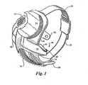
- FIG. 1 shows a perspective view of the implanted portion of the preferred retinal prosthesis.
- a flexible circuit 1 includes a flexible circuit electrode array 10 which is mounted by a retinal tack (not shown) or similar means to the epiretinal surface.
- the flexible circuit electrode array 10 is electrically coupled by a flexible circuit cable 12, which pierces the sclera in the pars plana region, and is electrically coupled to an electronics package 14, external to the sclera.
- an electrode array fan tail 15 is formed of molded silicone and attaches the electrode array cable 12 to a molded body 18 to reduce possible damage from any stresses applied during implantation.
- the electronics package 14 is electrically coupled to a secondary inductive coil 16.
- the secondary inductive coil 16 is made from wound wire.
- the secondary inductive coil 16 may be made from a flexible circuit polymer sandwich with wire traces deposited between layers of flexible circuit polymer.
- the electronics package 14 and secondary inductive coil 16 are held together by the molded body 18.
- the molded body 18 holds the electronics package 14 and secondary inductive coil 16 end to end. This is beneficial as it reduces the height the entire device rises above the sclera.
- the design of the electronic package (described below) along with a molded body 18 which holds the secondary inductive coil 16 and electronics package 14 in the end to end orientation minimizes the thickness or height above the sclera of the entire device. This is important to minimize any obstruction of natural eye movement.
- the molded body 18 may also include suture tabs 20.
- the molded body 18 narrows to form a strap 22 which surrounds the sclera and holds the molded body 18, secondary inductive coil 16, and electronics package 14 in place.
- the molded body 18, suture tabs 20 and strap 22 are preferably an integrated unit made of silicone elastomer. Silicone elastomer can be formed in a pre-curved shape to match the curvature of a typical sclera. However, silicone remains flexible enough to accommodate implantation and to adapt to variations in the curvature of an individual sclera.
- the secondary inductive coil 16 and molded body 18 are preferably oval shaped.
- a strap 22 can better support an oval shaped secondary inductive coil 16.
- a sleeve or coating 50 that promotes healing of the sclerotomy.
- Polymers such as polyimide, which may be used to form the flexible circuit cable 12 and flexible circuit electrode array 10, are generally very smooth and do not promote a good bond between the flexible circuit cable 12 and scleral tissue.
- a sleeve or coating of polyester, collagen, silicone, Gore-tex or similar material would bond with scleral tissue and promote healing.
- a porous material will allow scleral tissue to grow into the pores promoting a good bond.
- the entire implant is attached to and supported by the sclera: An eye moves constantly. The eye moves to scan a scene and also has a jitter motion to improve acuity. Even though such motion is useless in the blind, it often continues long after a person has lost their sight.
- eye motion does not cause any flexing which might fatigue, and eventually damage, the device.
- FIG. 2 shows side view of the implanted portion of the retinal prosthesis, in particular, emphasizing the strap fan tail 24.
- the secondary inductive coil 16 and molded body 18 must also follow the strap 22 under the lateral rectus muscle on the side of the sclera.
- the implanted portion of the retinal prosthesis is very delicate. It is easy to tear the molded body 18 or break wires in the secondary inductive coil 16 or electrode array cable 12 .
- the molded body 18 is shaped in the form of a strap fan tail 24 on the end opposite the electronics package 14 .
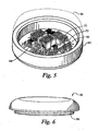
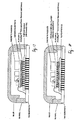
- Figure 3 shows the hermetic electronics package 14 is composed of a ceramic substrate 60 brazed to a metal case wall 62 which is enclosed by a laser welded metal lid 84 .
- the metal of the wall 62 and metal lid 84 may be any biocompatible metal such as Titanium, niobium, platinum, iridium, palladium or combinations of such metals.
- the ceramic substrate is preferably alumina but may include other ceramics such as zirconia.
- the ceramic substrate 60 includes vias (not shown) made from biocompatible metal and a ceramic binder using thick-film techniques.
- the biocompatible metal and ceramic binder is preferably platinum flakes in a ceramic paste or frit which is the ceramic used to make the substrate. After the vias have been filled, the substrate 60 is fired and lapped to thickness.
- the firing process causes the ceramic to vitrify biding the ceramic of the substrate with the ceramic of the paste forming a hermetic bond.
- Thin-film metallization 66 is applied to both the inside and outside surfaces of the ceramic substrate 60 and an ASIC (Application Specific Integrated Circuit) integrated circuit chip 64 is bonded to the thin film metallization on the inside of the ceramic substrate 60 .
- ASIC Application Specific Integrated Circuit
- the inside thin film metallization 66 includes a gold layer to allow electrical connection using wire bonding.
- the inside film metallization includes preferably two to three layers with a preferred gold top layer.
- the next layer to the ceramic is a titanium or tantalum or mixture or alloy thereof.
- the next layer is preferably palladium or platinum layer or an alloy thereof. All these metals are biocompatible.
- the preferred metallization includes a titanium, palladium and gold layer. Gold is a preferred top layer because it is corrosion resistant and can be cold bonded with gold wire.
- the outside thin film metallization includes a titanium adhesion layer and a platinum layer for connection to platinum electrode array traces. Platinum can be substituted by palladium or palladium/platinum alloy. If gold-gold wire bonding is desired a gold top layer is applied.
- the package wall 62 is brazed to the ceramic substrate 60 in a vacuum furnace using a biocompatible braze material in the braze joint.
- the braze material is a nickel titanium alloy.
- the braze temperature is approximately 1000° Celsius. Therefore the vias and thin film metallization 66 must be selected to withstand this temperature. Also, the electronics must be installed after brazing.
- the chip 64 is installed inside the package using thermocompression flip-chip technology. The chip is underfilled with epoxy to avoid connection failures due to thermal mismatch or vibration.
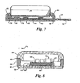
- Figures 4 and 5 show off-chip electrical components 70 , which may include capacitors, diodes, resistors or inductors (passives), are installed on a stack substrate 72 attached to the back of the chip 64 , and connections between the stack substrate 72 and ceramic substrate 60 are made using gold wire bonds 82 .
- the stack substrate 72 is attached to the chip 64 with non-conductive epoxy, and the passives 70 are attached to the stack substrate 72 with conductive epoxy.
- Figure 6 shows the electronics package 14 is enclosed by a metal lid 84 that, after a vacuum bake-out to remove volatiles and moisture, is attached using laser welding.
- a getter moisture absorbent material
- the metal lid 84 further has a metal lip 86 to protect components from the welding process and further insure a good hermetic seal.
- the entire package is hermetically encased. Hermeticity of the vias, braze, and the entire package is verified throughout the manufacturing process.
- the cylindrical package was designed to have a low profile to minimize its impact on the eye when implanted.
- the implant secondary inductive coil 16 which provides a means of establishing the inductive link between the external video processor (not shown) and the implanted device, preferably consists of gold wire.
- the wire is insulated with a layer of silicone.
- the secondary inductive coil 16 is oval shaped.
- the conductive wires are wound in defined pitches and curvature shape to satisfy both the electrical functional requirements and the surgical constraints.
- the secondary inductive coil 16, together with the tuning capacitors in the chip 64, forms a parallel resonant tank that is tuned at the carrier frequency to receive both power and data.
- Figure 7 shows the flexible circuit 1, includes platinum conductors 94 insulated from each other and the external environment by a biocompatible dielectric polymer 96, preferably polyimide.
- One end of the array contains exposed electrode sites that are placed in close proximity to the retinal surface 10.
- the other end contains bond pads 92 that permit electrical connection to the electronics package 14.
- the electronic package 14 is attached to the flexible circuit 1 using a flip-chip bumping process, and epoxy underfilled. In the flip-chip bumping process, bumps containing conductive adhesive placed on bond pads 92 and bumps containing conductive adhesive placed on the electronic package 14 are aligned and melted to build a conductive connection between the bond pads 92 and the electronic package 14.
- Leads 76 for the secondary inductive coil 16 are attached to gold pads 78 on the ceramic substrate 60 using thermal compression bonding, and are then covered in epoxy.
- the electrode array cable 12 is laser welded to the assembly junction and underfilled with epoxy.
- the junction of the secondary inductive coil 16, array 1, and electronic package 14 are encapsulated with a silicone overmold 90 that connects them together mechanically. When assembled, the hermetic electronics package 14 sits about 3mm away from the end of the secondary inductive coil.
- the implant device Since the implant device is implanted just under the conjunctiva it is possible to irritate or even erode through the conjunctiva. Eroding through the conjunctiva leaves the body open to infection. We can do several things to lessen the likelihood of conjunctiva irritation or erosion. First, it is important to keep the over all thickness of the implant to a minimum. Even though it is advantageous to mount both the electronics package 14 and the secondary inductive coil 16 on the lateral side of the sclera, the electronics package 14 is mounted higher than, but not covering, the secondary inductive coil 16. In other words the thickness of the secondary inductive coil 16 and electronics package should not be cumulative.
- the protective material can be provided as a flap attached to the implant device or a separate piece placed by the surgeon at the time of implantation. Further material over the scleratomy will promote healing and sealing of the scleratomy. Suitable materials include Dacron, Teflon (polytetraflouroethylene or PTFE), Goretex (ePTFE) Tutoplast (sterilized sclera), Mersilene (Polyester) or silicone.
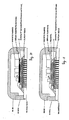
- Figure 8 shows the package 14 containing a ceramic substrate 60, with metallized vias 65 and thin-film metallization 66.
- the package 14 contains a metal case wall 62 which is connected to the ceramic substrate 60 by braze joint 61.
- On the ceramic substrate 60 an underfill 69 is applied.
- On the underfill 69 an integrated circuit chip 64 is positioned.
- On the integrated circuit chip 64 a ceramic hybrid substrate 68 is positioned.
- On the ceramic hybrid substrate 68 passives 70 are placed. Wirebonds 67 are leading from the ceramic substrate 60 to the ceramic hybrid substrate 68.
- a metal lid 84 is connected to the metal case wall 62 by laser welded joint 63 whereby the package 14 is sealed.
- Figure 9 shows a perspective view of the implanted portion of the preferred retinal prosthesis which is an alternative to the retinal prosthesis shown in figure 1 .
- the electronics package 14 is electrically coupled to a secondary inductive coil 16.
- the secondary inductive coil 16 is made from wound wire.
- the secondary inductive coil 16 may be made from a flexible circuit polymer sandwich with wire traces deposited between layers of flexible circuit polymer.
- the electronics package 14 and secondary inductive coil 16 are held together by the molded body 18.
- the molded body 18 holds the electronics package 14 and secondary inductive coil 16 end to end.
- the secondary inductive coil 16 is placed around the electronics package 14 in the molded body 18.
- the molded body 18 holds the secondary inductive coil 16 and electronics package 14 in the end to end orientation and minimizes the thickness or height above the sclera of the entire device.
- Lid 84 and case wall 62 may also contain titanium or titanium alloy or other metals and metal alloys including platinum, palladium, gold, silver, ruthenium, or ruthenium oxide.
- Lid 84 and case wall 62 may also contain a polymer, copolymer or block copolymer or polymer mixtures or polymer multilayer containing parylene, polyimide, silicone, epoxy, or PEEKTM polymer.
- Via substrate may be preferably contain alumina or zirconia with platinum vias.
- Figure 15 shows one stack assembly.
- One stack means that all of the parts are on a chip, with our without a separate demux.
- a via substrate is placed on the bottom below a flip IC which includes RF Transceiver, power recovery, drivers, and an optional demux.
- Figures 12, figure 13 and figure 14 show two stack assemblies.
- Figure 16 shows a folded stack assembly.
- Figure 12 shows a ceramic substrate next to RF transceiver/power recovery chip and both placed on a flipchip driver/demux.
- Figure 13 shows ceramic substrate on a flipchip driver/demux.
- RF transceiver/power recovery chip is provided on the ceramic substrate.
- Figure 14 shows ceramic substrate on to of a flipchip driver/demux.
- RF transceiver/power recovery chip is provided not directly on the ceramic substrate.
- the difference between figure 13 and figure 14 is that in figure 13 the ceramic substrate is in direct contact with RF transceiver/power recovery chip but not in figure 14 .
- the substrate can be ceramic but also any kind of polymer or glass.
- Figure 16 shows a folded stack substrate and a flipchip demux on the bottom and an IC placed on the flip chip demux. The substrate is folded twice.
- Figure 10 and figure 11 show a three stack assembly.
- a three stack demux flip-chip bonded to substrate with chip and hybrid wire-bonded above is preferred.
- Figure 10 shows a ceramic substrate on a IC including a RF transceiver/power recovery drivers and the IC is placed on a flipchip driver/demux.
- Figure 11 shows a similar assembly as figure 10 however the ceramic substrate is placed on pedestal which is placed between the substrate and the IC.
- Figure 17 and figure 18 show additional flip chip configurations. Both figures have a similar assembly. However, in figure 17 the IC is bonded to flipchip demux by a bump bond. In figure 18 a double sided multilayer ceramic substrate is bonded to the IC by a bump bond.
- a through via means that via goes through the IC.
- a bump bond to IC and then bump bond to IC to passive substrate or demux is possible. Bond pads on IC to line up with vias to eliminate the inside metallization can be provided.
- Driver IC flipchip can be bonded to substrate with passives. Demux flip-chip can be bonded to via substrate and the two substrates can be wire-bonded or flex circuit bonded together. Driver portion can be moved to demux chip and everything else to a separate chip to reduce interconnect lines.
- Two stack chip can be provided with smaller chip (RF and demux) and hybrid above. It may include wire-bonds directly from the Hybrid to the chip. Chip may include a demux driver on the same wafer.
- Figure 19 and figure 20 show different variations of the lid shape. Possible is a concave lid to conform to eye.
- Figure 21 and figure 22 are cross-sections the package showing interconnects in detail. Both figures show redistribution routings and interconnect on the top and the bottom of via substrate. Redistribution routing on top of the via substrate and the braze stop on top of the via substrate contain preferably metals like Ti, Zr, Fe, Ru, Co, Rh, Ir, Ni, Pd, Pt, Cu, Ag, Au, mixtures, layers or alloys thereof. The top layer of the top redistribution routing is gold or gold alloy. Redistribution routing on bottom of the via substrate and the braze stop on top of the via substrate contain preferably metals like Ti, Zr, Fe, Ru, Co, Rh, Ir, Ni, Pd, Pt, Cu, Ag, Au, mixtures, layers or alloys thereof.
- the top layer of the top redistribution routing is platinum or platinum alloy. Interconnect and redistribution routing is the connection the bond between flexible circuit and via substrate on the bottom of the substrate and a connection between the chip and the substrate on top of the substrate.
- the walls in figure 22 show the same braze metal as mentioned before as a flange.
Claims (14)
- Implantierbare Vorrichtung, die Folgendes umfasst:ein Substrat mit einem elektrisch nicht leitfähigen Abschnitt;eine Vielzahl elektrisch leitfähiger Durchführungen, die durch den elektrisch nicht leitfähigen Abschnitt hindurch verlaufen, wobei die Durchführungen und der elektrisch nicht leitfähige Abschnitt das Substrat bilden;Metallbahnen auf dem Substrat, die elektrisch mit den leitfähigen Durchführungen verbunden sind;eine mit den Metallbahnen verbundene Schaltung undeine durch eine Lötstelle mit dem Substrat verbundene Abdeckung, wobei die Abdeckung und das Substrat ein luftdichtes Gehäuse bilden;dadurch gekennzeichnet, dass die Vorrichtung ferner Folgendes umfasst:eine Lötstoppbahn, die die Metallbahnen umgibt;wobei die Lötstoppbahn verhindert, dass die Lötstelle mit den Metallbahnen in Berührung kommt.
- Implantierbare Vorrichtung nach Anspruch 1, worin die elektrisch leitfähigen Durchführungen eine Metall- und Keramikpaste sind, die gemeinsam mit dem nicht leitfähigen Abschnitt gebrannt werden, um eine hermetische Abdichtung zu bilden.
- Implantierbare Vorrichtung nach Anspruch 1, worin die Metallbahnen so ausgewählt sind, dass sie Löttemperaturen standhalten.
- Implantierbare Vorrichtung nach Anspruch 1, worin die Metallbahnen ein oder mehrere der Metalle Titan, Tantal, Gold, Palladium, Platin oder Schichten oder Legierungen davon umfassen.
- Implantierbare Vorrichtung nach Anspruch 1, die ferner einen flexiblen Schaltungskontakthöcker umfasst, der über leifähige Kontakthöcker an das Substrat gebondet ist.
- Implantierbare Vorrichtung nach Anspruch 5, die ferner weitere Metallbahnen, die auf dem starren Substrat abgeschieden sind und mit den elektrisch leitfähigen Durchführungen in Kontakt stehen, sowie einen flexiblen Schaltungskontakthöcker umfasst, der über leifähige Kontakthöcker an die Metallbahnen gebondet ist.
- Implantierbare Vorrichtung nach Anspruch 5 oder 6, worin die flexible Schaltung eine Elektrodenanordnung ist, die zur Stimulation von Gewebe geeignet ist.
- Implantierbare Vorrichtung nach Anspruch 5, 6 oder 7, worin die leitfähigen Kontakthöcker zumindest ein leitfähiges Polymer enthalten.
- Implantierbare Vorrichtung nach Anspruch 8, worin die leitfähigen Kontakthöcker zumindest ein leitfähiges Epoxy oder Polyimid enthalten.
- Implantierbare Vorrichtung nach Anspruch 1, worin die leitfähigen Kontakthöcker mit einem oder mehreren Metallen gefüllt sind, das/die aus folgender Gruppe ausgewählt ist/sind: Silber, Platin, Iridium, Titan, Platinlegierungen, Iridiumlegierungen oder Titanlegierungen oder Gemischen davon.
- Implantierbare Vorrichtung nach Anspruch 10, worin die Metalle oder Metalllegierungen staub-, flocken- oder pulverförmig vorliegen.
- Implantierbare Vorrichtung nach einem der Ansprüche 1 bis 11, worin die implantierbare Vorrichtung zwei oder mehr integrierte Schaltungen enthält.
- Implantierbare Vorrichtung nach einem der Ansprüche 1 bis 12, worin die Schaltung eine Flip-Chip-Schaltung ist, die an die Metallbahnen gebondet ist.
- Implantierbare Vorrichtung nach einem der Ansprüche 1 bis 13, worin die Schaltung an die Metallbahnen drahtgebondet ist.
Applications Claiming Priority (3)
| Application Number | Priority Date | Filing Date | Title |
|---|---|---|---|
| US83871406P | 2006-08-18 | 2006-08-18 | |
| US88099407P | 2007-01-18 | 2007-01-18 | |
| EP07837025.1A EP2061549B1 (de) | 2006-08-18 | 2007-08-18 | Verpackung für eine implantierbare nervenstimulationsvorrichtung |
Related Parent Applications (2)
| Application Number | Title | Priority Date | Filing Date |
|---|---|---|---|
| EP07837025.1 Division | 2007-08-18 | ||
| EP07837025.1A Division-Into EP2061549B1 (de) | 2006-08-18 | 2007-08-18 | Verpackung für eine implantierbare nervenstimulationsvorrichtung |
Publications (2)
| Publication Number | Publication Date |
|---|---|
| EP2422842A1 EP2422842A1 (de) | 2012-02-29 |
| EP2422842B1 true EP2422842B1 (de) | 2013-07-17 |
Family
ID=38856239
Family Applications (3)
| Application Number | Title | Priority Date | Filing Date |
|---|---|---|---|
| EP11185514.4A Active EP2422842B1 (de) | 2006-08-18 | 2007-08-18 | Verpackung für eine implantierbare Nervenstimulationsvorrichtung |
| EP07837025.1A Revoked EP2061549B1 (de) | 2006-08-18 | 2007-08-18 | Verpackung für eine implantierbare nervenstimulationsvorrichtung |
| EP11185513.6A Active EP2422841B1 (de) | 2006-08-18 | 2007-08-18 | Verpackung für eine implantierbare Nervenstimulationsvorrichtung |
Family Applications After (2)
| Application Number | Title | Priority Date | Filing Date |
|---|---|---|---|
| EP07837025.1A Revoked EP2061549B1 (de) | 2006-08-18 | 2007-08-18 | Verpackung für eine implantierbare nervenstimulationsvorrichtung |
| EP11185513.6A Active EP2422841B1 (de) | 2006-08-18 | 2007-08-18 | Verpackung für eine implantierbare Nervenstimulationsvorrichtung |
Country Status (4)
| Country | Link |
|---|---|
| US (7) | US8374698B2 (de) |
| EP (3) | EP2422842B1 (de) |
| AU (1) | AU2007284422B2 (de) |
| WO (1) | WO2008021524A2 (de) |
Families Citing this family (88)
| Publication number | Priority date | Publication date | Assignee | Title |
|---|---|---|---|---|
| JP4958898B2 (ja) * | 2005-04-28 | 2012-06-20 | セカンド サイト メディカル プロダクツ インコーポレイテッド | 移植可能な神経刺激装置のパッケージ |
| US8836513B2 (en) | 2006-04-28 | 2014-09-16 | Proteus Digital Health, Inc. | Communication system incorporated in an ingestible product |
| EP2392258B1 (de) | 2005-04-28 | 2014-10-08 | Proteus Digital Health, Inc. | Pharma-Informatiksystem |
| US8802183B2 (en) | 2005-04-28 | 2014-08-12 | Proteus Digital Health, Inc. | Communication system with enhanced partial power source and method of manufacturing same |
| US8912908B2 (en) | 2005-04-28 | 2014-12-16 | Proteus Digital Health, Inc. | Communication system with remote activation |
| EP2422842B1 (de) * | 2006-08-18 | 2013-07-17 | Second Sight Medical Products, Inc. | Verpackung für eine implantierbare Nervenstimulationsvorrichtung |
| US20080103572A1 (en) | 2006-10-31 | 2008-05-01 | Medtronic, Inc. | Implantable medical lead with threaded fixation |
| WO2008112578A1 (en) | 2007-03-09 | 2008-09-18 | Proteus Biomedical, Inc. | In-body device having a deployable antenna |
| MY154217A (en) | 2008-08-13 | 2015-05-15 | Proteus Digital Health Inc | Ingestible circuitry |
| US7898074B2 (en) * | 2008-12-12 | 2011-03-01 | Helmut Eckhardt | Electronic devices including flexible electrical circuits and related methods |
| WO2010090706A2 (en) * | 2009-01-21 | 2010-08-12 | California Institute Of Technology | Pocket-enabled chip assembly for implantable devices |
| JP2010172667A (ja) * | 2009-02-02 | 2010-08-12 | Nidek Co Ltd | 電子素子のハーメチックシール方法、及び該方法を用いた生体埋植用機能デバイスユニット,視覚再生補助装置 |
| WO2010111403A2 (en) | 2009-03-25 | 2010-09-30 | Proteus Biomedical, Inc. | Probablistic pharmacokinetic and pharmacodynamic modeling |
| MX2011011506A (es) | 2009-04-28 | 2012-05-08 | Proteus Biomedical Inc | Marcadores de eventos ingeribles altamente confiables y metodos para utilizar los mismos. |
| KR20170121299A (ko) | 2010-04-07 | 2017-11-01 | 프로테우스 디지털 헬스, 인코포레이티드 | 소형의 섭취가능한 장치 |
| WO2012015756A2 (en) * | 2010-07-29 | 2012-02-02 | Proteus Biomedical, Inc. | Hybrid housing for implantable medical device |
| JP2014504902A (ja) | 2010-11-22 | 2014-02-27 | プロテウス デジタル ヘルス, インコーポレイテッド | 医薬品を有する摂取可能なデバイス |
| CA3106924C (en) | 2011-03-17 | 2023-04-18 | William R. Patterson | Implantable wireless neural device |
| CN102178999B (zh) * | 2011-04-29 | 2013-06-19 | 纽诺斯(天津)科技发展有限公司 | 植入式神经电极阵列系统及其制作方法 |
| WO2015112603A1 (en) | 2014-01-21 | 2015-07-30 | Proteus Digital Health, Inc. | Masticable ingestible product and communication system therefor |
| US9756874B2 (en) | 2011-07-11 | 2017-09-12 | Proteus Digital Health, Inc. | Masticable ingestible product and communication system therefor |
| US8841558B2 (en) | 2011-08-02 | 2014-09-23 | Medtronic Inc. | Hermetic feedthrough |
| CA2845778C (en) | 2011-08-25 | 2021-12-21 | Microchips, Inc. | Space-efficient containment devices and method of making same |
| US10427153B2 (en) | 2011-08-25 | 2019-10-01 | Microchips Biotech, Inc. | Systems and methods for sealing a plurality of reservoirs of a microchip element with a sealing grid |
| US9956396B2 (en) * | 2012-02-08 | 2018-05-01 | Medtronic Bakken Research Center B.V. | Thin film for a lead for brain applications |
| US10008443B2 (en) | 2012-04-30 | 2018-06-26 | California Institute Of Technology | Implant device |
| JP2015534539A (ja) | 2012-07-23 | 2015-12-03 | プロテウス デジタル ヘルス, インコーポレイテッド | 摂取可能構成要素を備える摂取可能事象マーカーを製造するための技法 |
| AU2013308541B2 (en) | 2012-08-31 | 2016-05-05 | Alfred E. Mann Foundation For Scientific Research | Feedback controlled coil driver for inductive power transfer |
| US9268909B2 (en) | 2012-10-18 | 2016-02-23 | Proteus Digital Health, Inc. | Apparatus, system, and method to adaptively optimize power dissipation and broadcast power in a power source for a communication device |
| WO2014120669A1 (en) | 2013-01-29 | 2014-08-07 | Proteus Digital Health, Inc. | Highly-swellable polymeric films and compositions comprising the same |
| WO2014146019A2 (en) | 2013-03-15 | 2014-09-18 | Alfred E. Mann Foundation For Scientific Research | High voltage monitoring successive approximation analog to digital converter |
| US10175376B2 (en) | 2013-03-15 | 2019-01-08 | Proteus Digital Health, Inc. | Metal detector apparatus, system, and method |
| JP6298145B2 (ja) | 2013-03-15 | 2018-03-20 | アルフレッド イー. マン ファウンデーション フォー サイエンティフィック リサーチ | 高速のターンオン時間をもつ電流検出複数出力電流刺激装置 |
| JP6842917B2 (ja) | 2013-05-03 | 2021-03-17 | アルフレッド イー. マン ファウンデーション フォー サイエンティフィック リサーチ | インプラント充電器ハンドシェイキングシステム及び方法 |
| US9221119B2 (en) | 2013-05-03 | 2015-12-29 | Alfred E. Mann Foundation For Scientific Research | High reliability wire welding for implantable devices |
| EP2991726B1 (de) | 2013-05-03 | 2018-07-25 | Alfred E. Mann Foundation for Scientific Research | Mehrzweigige stimulationselektrode für subkutane feldstimulation |
| CA2913074C (en) | 2013-05-30 | 2023-09-12 | Graham H. Creasey | Topical neurological stimulation |
| US11229789B2 (en) | 2013-05-30 | 2022-01-25 | Neurostim Oab, Inc. | Neuro activator with controller |
| WO2015004673A1 (en) * | 2013-07-11 | 2015-01-15 | Newpace Ltd. | Battery and electronics integration in an implantable medical device |
| US10610693B2 (en) | 2013-07-11 | 2020-04-07 | Newpace Ltd. | Battery and electronics integration in a flexible implantable medical device |
| JP6494625B2 (ja) | 2013-07-29 | 2019-04-03 | アルフレッド イー. マン ファウンデーション フォー サイエンティフィック リサーチ | 無線リンクによる埋め込み充電場制御 |
| CA3075310C (en) | 2013-07-29 | 2022-04-05 | Alfred E. Mann Foundation For Scientific Research | Microprocessor controlled class e driver |
| JP6503351B2 (ja) | 2013-07-29 | 2019-04-17 | アルフレッド イー. マン ファウンデーション フォー サイエンティフィック リサーチ | 埋め込み可能なデバイス用の高効率磁気リンク |
| US9781842B2 (en) | 2013-08-05 | 2017-10-03 | California Institute Of Technology | Long-term packaging for the protection of implant electronics |
| US9796576B2 (en) | 2013-08-30 | 2017-10-24 | Proteus Digital Health, Inc. | Container with electronically controlled interlock |
| US10084880B2 (en) | 2013-11-04 | 2018-09-25 | Proteus Digital Health, Inc. | Social media networking based on physiologic information |
| US10674928B2 (en) | 2014-07-17 | 2020-06-09 | Medtronic, Inc. | Leadless pacing system including sensing extension |
| US9399140B2 (en) | 2014-07-25 | 2016-07-26 | Medtronic, Inc. | Atrial contraction detection by a ventricular leadless pacing device for atrio-synchronous ventricular pacing |
| US10682521B2 (en) | 2014-08-15 | 2020-06-16 | Axonics Modulation Technologies, Inc. | Attachment devices and associated methods of use with a nerve stimulation charging device |
| CN106999709B (zh) | 2014-08-15 | 2021-07-09 | 艾克索尼克斯股份有限公司 | 用于与可植入神经刺激器一起使用的集成肌电图临床医生程控器 |
| US9802038B2 (en) | 2014-08-15 | 2017-10-31 | Axonics Modulation Technologies, Inc. | Implantable lead affixation structure for nerve stimulation to alleviate bladder dysfunction and other indication |
| CN107073258B (zh) | 2014-08-15 | 2020-02-21 | 艾克索尼克斯调制技术股份有限公司 | 用于基于神经定位来进行神经刺激电极配置的系统和方法 |
| EP3180072B1 (de) | 2014-08-15 | 2018-11-28 | Axonics Modulation Technologies Inc. | Positionierung einer elektromyografischen elektrode und stimulationstitrierung in einem nervenstimulierungssystem zur behandlung von hyperaktiver blase |
| EP3180071B1 (de) | 2014-08-15 | 2021-09-22 | Axonics, Inc. | Externe impulsgeneratorvorrichtung und zugehörige system zur versuchsnervenstimulation |
| US9492669B2 (en) | 2014-11-11 | 2016-11-15 | Medtronic, Inc. | Mode switching by a ventricular leadless pacing device |
| US9492668B2 (en) | 2014-11-11 | 2016-11-15 | Medtronic, Inc. | Mode switching by a ventricular leadless pacing device |
| US9623234B2 (en) | 2014-11-11 | 2017-04-18 | Medtronic, Inc. | Leadless pacing device implantation |
| US9724519B2 (en) | 2014-11-11 | 2017-08-08 | Medtronic, Inc. | Ventricular leadless pacing device mode switching |
| US10507321B2 (en) | 2014-11-25 | 2019-12-17 | Medtronic Bakken Research Center B.V. | Multilayer structure and method of manufacturing a multilayer structure |
| US9289612B1 (en) | 2014-12-11 | 2016-03-22 | Medtronic Inc. | Coordination of ventricular pacing in a leadless pacing system |
| AU2016205049B2 (en) | 2015-01-09 | 2020-05-14 | Axonics Modulation Technologies, Inc. | Improved antenna and methods of use for an implantable nerve stimulator |
| CN107427685B (zh) | 2015-01-09 | 2021-09-21 | 艾克索尼克斯股份有限公司 | 与神经刺激充电设备一起使用的附接设备及相关联方法 |
| AU2016205047B2 (en) | 2015-01-09 | 2020-07-02 | Axonics Modulation Technologies, Inc. | Patient remote and associated methods of use with a nerve stimulation system |
| FR3031898B1 (fr) * | 2015-01-28 | 2017-02-24 | Commissariat Energie Atomique | Dispositif et methode de rehabilitation prothetique de la retine |
| US11077301B2 (en) | 2015-02-21 | 2021-08-03 | NeurostimOAB, Inc. | Topical nerve stimulator and sensor for bladder control |
| AU2016291554B2 (en) | 2015-07-10 | 2021-01-07 | Axonics Modulation Technologies, Inc. | Implantable nerve stimulator having internal electronics without ASIC and methods of use |
| US11051543B2 (en) | 2015-07-21 | 2021-07-06 | Otsuka Pharmaceutical Co. Ltd. | Alginate on adhesive bilayer laminate film |
| CN108024851A (zh) * | 2015-08-28 | 2018-05-11 | 加州理工学院 | 植入装置及其制造方法 |
| US10195423B2 (en) | 2016-01-19 | 2019-02-05 | Axonics Modulation Technologies, Inc. | Multichannel clip device and methods of use |
| US9517338B1 (en) | 2016-01-19 | 2016-12-13 | Axonics Modulation Technologies, Inc. | Multichannel clip device and methods of use |
| CN108697886B (zh) | 2016-01-29 | 2022-11-08 | 艾克索尼克斯股份有限公司 | 用于频率调整以优化可植入神经刺激器的充电的方法和系统 |
| JP7072510B2 (ja) | 2016-02-12 | 2022-05-20 | アクソニクス インコーポレイテッド | 外部パルス発生器デバイスおよび試験的神経刺激のための関連方法 |
| CN108701956B (zh) * | 2016-03-02 | 2021-06-04 | 索尼公司 | 发光装置和制造发光装置的方法 |
| US11623082B2 (en) * | 2016-03-07 | 2023-04-11 | Cortigent, Inc. | Flexible circuit peripheral nerve stimulator with low profile hybrid assembly |
| US11207527B2 (en) | 2016-07-06 | 2021-12-28 | Cardiac Pacemakers, Inc. | Method and system for determining an atrial contraction timing fiducial in a leadless cardiac pacemaker system |
| CN109843149B (zh) | 2016-07-22 | 2020-07-07 | 普罗秋斯数字健康公司 | 可摄入事件标记的电磁感测和检测 |
| CN109963499B (zh) | 2016-10-26 | 2022-02-25 | 大冢制药株式会社 | 用于制造具有可吸收事件标记器的胶囊的方法 |
| WO2019094365A1 (en) | 2017-11-07 | 2019-05-16 | Neurostim Oab, Inc. | Non-invasive nerve activator with adaptive circuit |
| US11154708B2 (en) | 2017-12-22 | 2021-10-26 | Marc Possover | Implantable neurostimulator and methods for implanting and using same |
| WO2019120568A1 (de) * | 2017-12-22 | 2019-06-27 | Marc Possover | System zur neuromodulation |
| CN108211118B (zh) * | 2017-12-23 | 2021-11-26 | 深圳先进技术研究院 | 植入式封装体及其制造方法和植入式医疗器件 |
| CN108172553A (zh) * | 2018-01-17 | 2018-06-15 | 杭州暖芯迦电子科技有限公司 | 一种视网膜假体植入芯片的封装结构及其封装方法 |
| CA3090810A1 (en) | 2018-02-22 | 2019-08-29 | Axonics Modulation Technologies, Inc. | Neurostimulation leads for trial nerve stimulation and methods of use |
| US11642537B2 (en) | 2019-03-11 | 2023-05-09 | Axonics, Inc. | Charging device with off-center coil |
| US11848090B2 (en) | 2019-05-24 | 2023-12-19 | Axonics, Inc. | Trainer for a neurostimulator programmer and associated methods of use with a neurostimulation system |
| US11439829B2 (en) | 2019-05-24 | 2022-09-13 | Axonics, Inc. | Clinician programmer methods and systems for maintaining target operating temperatures |
| CA3144957A1 (en) | 2019-06-26 | 2020-12-30 | Neurostim Technologies Llc | Non-invasive nerve activator with adaptive circuit |
| CA3152451A1 (en) | 2019-12-16 | 2021-06-24 | Michael Bernard Druke | Non-invasive nerve activator with boosted charge delivery |
Family Cites Families (75)
| Publication number | Priority date | Publication date | Assignee | Title |
|---|---|---|---|---|
| GB1319774A (en) | 1969-06-26 | 1973-06-06 | Nat Res Dev | Visual prosthetic device |
| US4451540A (en) * | 1982-08-30 | 1984-05-29 | Isotronics, Inc. | System for packaging of electronic circuits |
| US4798801A (en) * | 1983-10-11 | 1989-01-17 | Phillips Petroleum Company | Production of methane by anaerobic fermentation of waste materials |
| US4573481A (en) | 1984-06-25 | 1986-03-04 | Huntington Institute Of Applied Research | Implantable electrode array |
| US4628933A (en) | 1985-07-23 | 1986-12-16 | Michelson Robin P | Method and apparatus for visual prosthesis |
| US4727633A (en) * | 1985-08-08 | 1988-03-01 | Tektronix, Inc. | Method of securing metallic members together |
| US5006286A (en) | 1986-03-31 | 1991-04-09 | Amp Incorporated | Polymeric electrical interconnection apparatus and method of use |
| US4837049A (en) | 1986-06-17 | 1989-06-06 | Alfred E. Mann Foundation For Scientific Research | Method of making an electrode array |
| US4759300A (en) * | 1987-10-22 | 1988-07-26 | Balboa Pacific Corporation | Method and apparatus for the pyrolysis of waste products |
| US4818405A (en) * | 1988-01-15 | 1989-04-04 | Vroom Kenneth B | Sludge treatment |
| US4880533A (en) * | 1988-06-09 | 1989-11-14 | John Hondulas | Apparatus and system for treating waste water and sludge |
| US4897195A (en) * | 1989-04-11 | 1990-01-30 | Erickson Stewart E | System and process for anaerobic digestion of waste materials |
| US5215088A (en) | 1989-11-07 | 1993-06-01 | The University Of Utah | Three-dimensional electrode device |
| US5611140A (en) | 1989-12-18 | 1997-03-18 | Epoxy Technology, Inc. | Method of forming electrically conductive polymer interconnects on electrical substrates |
| US5109844A (en) | 1990-10-11 | 1992-05-05 | Duke University | Retinal microstimulation |
| DE69207507T2 (de) * | 1991-02-25 | 1996-09-12 | Sumitomo Electric Industries | Leiterplatte |
| US5527464A (en) * | 1991-06-24 | 1996-06-18 | Bartha; Istvan | Method and system for the treatment and utilization of waste products |
| US5616163A (en) * | 1991-09-20 | 1997-04-01 | Halfter; Georg | Method for processing animal excrement and liquid manure |
| US5468936A (en) | 1993-03-23 | 1995-11-21 | Philip Morris Incorporated | Heater having a multiple-layer ceramic substrate and method of fabrication |
| US5670824A (en) * | 1994-12-22 | 1997-09-23 | Pacsetter, Inc. | Vertically integrated component assembly incorporating active and passive components |
| US6014586A (en) * | 1995-11-20 | 2000-01-11 | Pacesetter, Inc. | Vertically integrated semiconductor package for an implantable medical device |
| US5646446A (en) * | 1995-12-22 | 1997-07-08 | Fairchild Space And Defense Corporation | Three-dimensional flexible assembly of integrated circuits |
| CA2249602A1 (en) * | 1996-04-04 | 1997-10-16 | Medtronic, Inc. | Living tissue stimulation and recording techniques |
| US6057598A (en) * | 1997-01-31 | 2000-05-02 | Vlsi Technology, Inc. | Face on face flip chip integration |
| DE19707046A1 (de) | 1997-02-21 | 1998-08-27 | Rolf Prof Dr Ing Eckmiller | Lernfähiger "Active Vision" Implant Encoder |
| US6458157B1 (en) | 1997-08-04 | 2002-10-01 | Suaning Gregg Joergen | Retinal stimulator |
| US5902326A (en) * | 1997-09-03 | 1999-05-11 | Medtronic, Inc. | Optical window for implantable medical devices |
| US6144866A (en) * | 1998-10-30 | 2000-11-07 | Medtronic, Inc. | Multiple sensor assembly for medical electric lead |
| US5905639A (en) * | 1997-09-29 | 1999-05-18 | Raytheon Company | Three-dimensional component stacking using high density multichip interconnect decals and three-bond daisy-chained wedge bonds |
| US6007578A (en) * | 1997-10-08 | 1999-12-28 | Ras Holding Corp | Scleral prosthesis for treatment of presbyopia and other eye disorders |
| US5954751A (en) * | 1998-01-15 | 1999-09-21 | Intermedics Inc. | Implantable defibrillator with stacked transistor subassemblies |
| US5935155A (en) | 1998-03-13 | 1999-08-10 | John Hopkins University, School Of Medicine | Visual prosthesis and method of using same |
| ES2306525T3 (es) * | 1998-08-26 | 2008-11-01 | Sensors For Medicine And Science, Inc. | Dispositivos de deteccion basados en optica. |
| DE60042155D1 (de) | 1999-03-24 | 2009-06-18 | Second Sight Medical Prod Inc | Retinale farbprothese zur wiederherstellung des farbsehens |
| US8180453B2 (en) * | 1999-03-24 | 2012-05-15 | Second Sight Medical Products, Inc. | Electrode array for neural stimulation |
| US6451589B1 (en) * | 1999-10-25 | 2002-09-17 | Ghd, Inc. | Method and apparatus for solids processing |
| US6414884B1 (en) * | 2000-02-04 | 2002-07-02 | Lucent Technologies Inc. | Method and apparatus for securing electronic circuits |
| US6414835B1 (en) * | 2000-03-01 | 2002-07-02 | Medtronic, Inc. | Capacitive filtered feedthrough array for an implantable medical device |
| DE60135100D1 (de) * | 2000-03-24 | 2008-09-11 | Cymbet Corp | E mit ultradünnem elektrolyten |
| US6387281B2 (en) * | 2000-03-25 | 2002-05-14 | R3 Management Limited | Processes and apparatus for treating sewage or like sludge |
| US6258626B1 (en) * | 2000-07-06 | 2001-07-10 | Advanced Semiconductor Engineering, Inc. | Method of making stacked chip package |
| US6361716B1 (en) | 2000-07-20 | 2002-03-26 | Dow Corning Corporation | Silicone composition and electrically conductive silicone adhesive formed therefrom |
| JP3581086B2 (ja) * | 2000-09-07 | 2004-10-27 | 松下電器産業株式会社 | 半導体装置 |
| US7103416B2 (en) | 2001-01-16 | 2006-09-05 | Second Sight Medical Products, Inc. | Visual prosthesis including enhanced receiving and stimulating portion |
| US6942798B2 (en) * | 2001-01-19 | 2005-09-13 | Miller, Iii Herman P. | Vacuum retort anaerobic digestion system and process |
| US7480988B2 (en) | 2001-03-30 | 2009-01-27 | Second Sight Medical Products, Inc. | Method and apparatus for providing hermetic electrical feedthrough |
| US6665191B2 (en) * | 2001-09-10 | 2003-12-16 | Cardiac Pacemakers, Inc. | Multi-folded printed wiring construction for an implantable medical device |
| AU2002348166A1 (en) * | 2001-11-16 | 2003-06-10 | Ch2M Hill, Inc. | Method and apparatus for the treatment of particulate biodegradable organic waste |
| US20040006264A1 (en) * | 2001-11-20 | 2004-01-08 | Mojarradi Mohammad M. | Neural prosthetic micro system |
| US20030109903A1 (en) | 2001-12-12 | 2003-06-12 | Epic Biosonics Inc. | Low profile subcutaneous enclosure |
| WO2003061537A1 (en) * | 2002-01-17 | 2003-07-31 | Masachusetts Eye And Ear Infirmary | Minimally invasive retinal prosthesis |
| US6718209B2 (en) | 2002-02-05 | 2004-04-06 | Second Sight Medical Products, Inc. | Retinal prosthesis with remote return electrode |
| US7211103B2 (en) | 2002-04-11 | 2007-05-01 | Second Sight Medical Products, Inc. | Biocompatible bonding method and electronics package suitable for implantation |
| US7142909B2 (en) * | 2002-04-11 | 2006-11-28 | Second Sight Medical Products, Inc. | Biocompatible bonding method and electronics package suitable for implantation |
| DE10227658B4 (de) * | 2002-06-20 | 2012-03-08 | Curamik Electronics Gmbh | Metall-Keramik-Substrat für elektrische Schaltkreise -oder Module, Verfahren zum Herstellen eines solchen Substrates sowie Modul mit einem solchen Substrat |
| CA2491018C (en) * | 2002-06-28 | 2013-06-18 | Advanced Bionics Corporation | Microstimulator having self-contained power source and bi-directional telemetry system |
| US6866779B1 (en) * | 2002-07-22 | 2005-03-15 | Western Environmental Engineering Company | Nitrogen recovery system and method |
| US7049691B2 (en) * | 2002-10-08 | 2006-05-23 | Chippac, Inc. | Semiconductor multi-package module having inverted second package and including additional die or stacked package on second package |
| US20040098124A1 (en) * | 2002-11-19 | 2004-05-20 | Freeman Jerre M. | Elongate scleral implants for the treatment of eye disorders such as presbyopia and glaucoma |
| US6692554B1 (en) * | 2002-12-10 | 2004-02-17 | Visteon Global Technologies, Inc. | Methane storage device |
| US8014878B2 (en) | 2005-04-28 | 2011-09-06 | Second Sight Medical Products, Inc. | Flexible circuit electrode array |
| US6940158B2 (en) * | 2003-05-30 | 2005-09-06 | Tessera, Inc. | Assemblies having stacked semiconductor chips and methods of making same |
| US7228181B2 (en) | 2004-04-06 | 2007-06-05 | Second Sight Medical Products, Inc. | Retinal prosthesis with side mounted inductive coil |
| US20050228467A1 (en) * | 2004-04-07 | 2005-10-13 | Guangqiang Jiang | Implantable miniature titanium to stainless steel connector |
| US7263403B2 (en) * | 2004-05-25 | 2007-08-28 | Second Sight Medical Products, Inc. | Retinal prosthesis |
| US7390294B2 (en) * | 2004-05-28 | 2008-06-24 | Ethicon Endo-Surgery, Inc. | Piezo electrically driven bellows infuser for hydraulically controlling an adjustable gastric band |
| US20060108676A1 (en) * | 2004-11-22 | 2006-05-25 | Punzalan Nelson V Jr | Multi-chip package using an interposer |
| US8068913B2 (en) | 2004-12-03 | 2011-11-29 | Second Sight Medical Products, Inc. | Visual prosthesis for improved circadian rhythms and method of improving the circadian rhythms |
| US7145076B2 (en) * | 2005-02-08 | 2006-12-05 | Greatbatch, Inc. | Method for minimizing stress in feedthrough capacitor filter assemblies |
| US7132754B1 (en) * | 2005-03-17 | 2006-11-07 | Alfred E. Mann Foundation For Scientific Research | Flip chip stack |
| JP4958898B2 (ja) * | 2005-04-28 | 2012-06-20 | セカンド サイト メディカル プロダクツ インコーポレイテッド | 移植可能な神経刺激装置のパッケージ |
| US7068491B1 (en) * | 2005-09-15 | 2006-06-27 | Medtronic, Inc. | Implantable co-fired electrical interconnect systems and devices and methods of fabrication therefor |
| WO2007035774A1 (en) | 2005-09-19 | 2007-03-29 | Second Sight Medical Products, Inc. | Retinal prosthesis with a new configuration |
| EP2422842B1 (de) * | 2006-08-18 | 2013-07-17 | Second Sight Medical Products, Inc. | Verpackung für eine implantierbare Nervenstimulationsvorrichtung |
| US8000804B1 (en) * | 2006-10-27 | 2011-08-16 | Sandia Corporation | Electrode array for neural stimulation |
-
2007
- 2007-08-18 EP EP11185514.4A patent/EP2422842B1/de active Active
- 2007-08-18 WO PCT/US2007/018315 patent/WO2008021524A2/en active Application Filing
- 2007-08-18 AU AU2007284422A patent/AU2007284422B2/en not_active Ceased
- 2007-08-18 EP EP07837025.1A patent/EP2061549B1/de not_active Revoked
- 2007-08-18 EP EP11185513.6A patent/EP2422841B1/de active Active
- 2007-08-18 US US11/893,939 patent/US8374698B2/en active Active
- 2007-10-26 US US11/924,709 patent/US8412339B2/en active Active
-
2011
- 2011-09-01 US US13/224,104 patent/US8406887B2/en active Active
-
2013
- 2013-03-01 US US13/783,225 patent/US8571672B2/en active Active
- 2013-10-08 US US14/049,056 patent/US8996118B2/en active Active
-
2015
- 2015-03-30 US US14/673,638 patent/US9713716B2/en active Active
-
2017
- 2017-06-21 US US15/629,196 patent/US10617868B2/en active Active
Also Published As
| Publication number | Publication date |
|---|---|
| EP2422841B1 (de) | 2013-10-09 |
| WO2008021524A2 (en) | 2008-02-21 |
| EP2061549A2 (de) | 2009-05-27 |
| US20110319963A1 (en) | 2011-12-29 |
| US20130178907A1 (en) | 2013-07-11 |
| WO2008021524A3 (en) | 2008-05-22 |
| US10617868B2 (en) | 2020-04-14 |
| US8571672B2 (en) | 2013-10-29 |
| AU2007284422A1 (en) | 2008-02-21 |
| US20170291028A1 (en) | 2017-10-12 |
| US8996118B2 (en) | 2015-03-31 |
| EP2422841A1 (de) | 2012-02-29 |
| US8374698B2 (en) | 2013-02-12 |
| US20080086173A1 (en) | 2008-04-10 |
| EP2061549B1 (de) | 2014-04-09 |
| US20140039588A1 (en) | 2014-02-06 |
| US8406887B2 (en) | 2013-03-26 |
| US20080058895A1 (en) | 2008-03-06 |
| US9713716B2 (en) | 2017-07-25 |
| EP2422842A1 (de) | 2012-02-29 |
| US8412339B2 (en) | 2013-04-02 |
| AU2007284422B2 (en) | 2011-06-02 |
| US20150202439A1 (en) | 2015-07-23 |
Similar Documents
| Publication | Publication Date | Title |
|---|---|---|
| US10617868B2 (en) | Package for an implantable neural stimulation device | |
| US9931507B2 (en) | Package for a retinal prosthesis | |
| US8954157B2 (en) | Implantable package to facilitate inspection | |
| AU2011223988B2 (en) | Package for an implantable retinal prosthesis |
Legal Events
| Date | Code | Title | Description |
|---|---|---|---|
| AC | Divisional application: reference to earlier application |
Ref document number: 2061549 Country of ref document: EP Kind code of ref document: P |
|
| AK | Designated contracting states |
Kind code of ref document: A1 Designated state(s): AT BE BG CH CY CZ DE DK EE ES FI FR GB GR HU IE IS IT LI LT LU LV MC MT NL PL PT RO SE SI SK TR |
|
| PUAI | Public reference made under article 153(3) epc to a published international application that has entered the european phase |
Free format text: ORIGINAL CODE: 0009012 |
|
| 17P | Request for examination filed |
Effective date: 20120314 |
|
| GRAP | Despatch of communication of intention to grant a patent |
Free format text: ORIGINAL CODE: EPIDOSNIGR1 |
|
| GRAS | Grant fee paid |
Free format text: ORIGINAL CODE: EPIDOSNIGR3 |
|
| GRAA | (expected) grant |
Free format text: ORIGINAL CODE: 0009210 |
|
| AC | Divisional application: reference to earlier application |
Ref document number: 2061549 Country of ref document: EP Kind code of ref document: P |
|
| AK | Designated contracting states |
Kind code of ref document: B1 Designated state(s): AT BE BG CH CY CZ DE DK EE ES FI FR GB GR HU IE IS IT LI LT LU LV MC MT NL PL PT RO SE SI SK TR |
|
| REG | Reference to a national code |
Ref country code: GB Ref legal event code: FG4D |
|
| REG | Reference to a national code |
Ref country code: CH Ref legal event code: EP |
|
| REG | Reference to a national code |
Ref country code: IE Ref legal event code: FG4D |
|
| REG | Reference to a national code |
Ref country code: AT Ref legal event code: REF Ref document number: 621780 Country of ref document: AT Kind code of ref document: T Effective date: 20130815 |
|
| REG | Reference to a national code |
Ref country code: DE Ref legal event code: R096 Ref document number: 602007031788 Country of ref document: DE Effective date: 20130912 |
|
| REG | Reference to a national code |
Ref country code: AT Ref legal event code: MK05 Ref document number: 621780 Country of ref document: AT Kind code of ref document: T Effective date: 20130717 |
|
| REG | Reference to a national code |
Ref country code: NL Ref legal event code: VDEP Effective date: 20130717 |
|
| REG | Reference to a national code |
Ref country code: LT Ref legal event code: MG4D |
|
| PG25 | Lapsed in a contracting state [announced via postgrant information from national office to epo] |
Ref country code: BE Free format text: LAPSE BECAUSE OF FAILURE TO SUBMIT A TRANSLATION OF THE DESCRIPTION OR TO PAY THE FEE WITHIN THE PRESCRIBED TIME-LIMIT Effective date: 20130717 Ref country code: AT Free format text: LAPSE BECAUSE OF FAILURE TO SUBMIT A TRANSLATION OF THE DESCRIPTION OR TO PAY THE FEE WITHIN THE PRESCRIBED TIME-LIMIT Effective date: 20130717 Ref country code: PT Free format text: LAPSE BECAUSE OF FAILURE TO SUBMIT A TRANSLATION OF THE DESCRIPTION OR TO PAY THE FEE WITHIN THE PRESCRIBED TIME-LIMIT Effective date: 20131118 Ref country code: CY Free format text: LAPSE BECAUSE OF FAILURE TO SUBMIT A TRANSLATION OF THE DESCRIPTION OR TO PAY THE FEE WITHIN THE PRESCRIBED TIME-LIMIT Effective date: 20130814 Ref country code: LT Free format text: LAPSE BECAUSE OF FAILURE TO SUBMIT A TRANSLATION OF THE DESCRIPTION OR TO PAY THE FEE WITHIN THE PRESCRIBED TIME-LIMIT Effective date: 20130717 Ref country code: IS Free format text: LAPSE BECAUSE OF FAILURE TO SUBMIT A TRANSLATION OF THE DESCRIPTION OR TO PAY THE FEE WITHIN THE PRESCRIBED TIME-LIMIT Effective date: 20131117 Ref country code: SE Free format text: LAPSE BECAUSE OF FAILURE TO SUBMIT A TRANSLATION OF THE DESCRIPTION OR TO PAY THE FEE WITHIN THE PRESCRIBED TIME-LIMIT Effective date: 20130717 |
|
| PG25 | Lapsed in a contracting state [announced via postgrant information from national office to epo] |
Ref country code: PL Free format text: LAPSE BECAUSE OF FAILURE TO SUBMIT A TRANSLATION OF THE DESCRIPTION OR TO PAY THE FEE WITHIN THE PRESCRIBED TIME-LIMIT Effective date: 20130717 Ref country code: FI Free format text: LAPSE BECAUSE OF FAILURE TO SUBMIT A TRANSLATION OF THE DESCRIPTION OR TO PAY THE FEE WITHIN THE PRESCRIBED TIME-LIMIT Effective date: 20130717 Ref country code: LV Free format text: LAPSE BECAUSE OF FAILURE TO SUBMIT A TRANSLATION OF THE DESCRIPTION OR TO PAY THE FEE WITHIN THE PRESCRIBED TIME-LIMIT Effective date: 20130717 Ref country code: NL Free format text: LAPSE BECAUSE OF FAILURE TO SUBMIT A TRANSLATION OF THE DESCRIPTION OR TO PAY THE FEE WITHIN THE PRESCRIBED TIME-LIMIT Effective date: 20130717 Ref country code: ES Free format text: LAPSE BECAUSE OF FAILURE TO SUBMIT A TRANSLATION OF THE DESCRIPTION OR TO PAY THE FEE WITHIN THE PRESCRIBED TIME-LIMIT Effective date: 20131028 Ref country code: GR Free format text: LAPSE BECAUSE OF FAILURE TO SUBMIT A TRANSLATION OF THE DESCRIPTION OR TO PAY THE FEE WITHIN THE PRESCRIBED TIME-LIMIT Effective date: 20131018 Ref country code: SI Free format text: LAPSE BECAUSE OF FAILURE TO SUBMIT A TRANSLATION OF THE DESCRIPTION OR TO PAY THE FEE WITHIN THE PRESCRIBED TIME-LIMIT Effective date: 20130717 |
|
| PG25 | Lapsed in a contracting state [announced via postgrant information from national office to epo] |
Ref country code: CY Free format text: LAPSE BECAUSE OF FAILURE TO SUBMIT A TRANSLATION OF THE DESCRIPTION OR TO PAY THE FEE WITHIN THE PRESCRIBED TIME-LIMIT Effective date: 20130717 |
|
| REG | Reference to a national code |
Ref country code: CH Ref legal event code: PL |
|
| PG25 | Lapsed in a contracting state [announced via postgrant information from national office to epo] |
Ref country code: MC Free format text: LAPSE BECAUSE OF FAILURE TO SUBMIT A TRANSLATION OF THE DESCRIPTION OR TO PAY THE FEE WITHIN THE PRESCRIBED TIME-LIMIT Effective date: 20130717 Ref country code: DK Free format text: LAPSE BECAUSE OF FAILURE TO SUBMIT A TRANSLATION OF THE DESCRIPTION OR TO PAY THE FEE WITHIN THE PRESCRIBED TIME-LIMIT Effective date: 20130717 Ref country code: CZ Free format text: LAPSE BECAUSE OF FAILURE TO SUBMIT A TRANSLATION OF THE DESCRIPTION OR TO PAY THE FEE WITHIN THE PRESCRIBED TIME-LIMIT Effective date: 20130717 Ref country code: CH Free format text: LAPSE BECAUSE OF NON-PAYMENT OF DUE FEES Effective date: 20130831 Ref country code: SK Free format text: LAPSE BECAUSE OF FAILURE TO SUBMIT A TRANSLATION OF THE DESCRIPTION OR TO PAY THE FEE WITHIN THE PRESCRIBED TIME-LIMIT Effective date: 20130717 Ref country code: LI Free format text: LAPSE BECAUSE OF NON-PAYMENT OF DUE FEES Effective date: 20130831 Ref country code: RO Free format text: LAPSE BECAUSE OF FAILURE TO SUBMIT A TRANSLATION OF THE DESCRIPTION OR TO PAY THE FEE WITHIN THE PRESCRIBED TIME-LIMIT Effective date: 20130717 Ref country code: EE Free format text: LAPSE BECAUSE OF FAILURE TO SUBMIT A TRANSLATION OF THE DESCRIPTION OR TO PAY THE FEE WITHIN THE PRESCRIBED TIME-LIMIT Effective date: 20130717 |
|
| REG | Reference to a national code |
Ref country code: IE Ref legal event code: MM4A |
|
| PLBE | No opposition filed within time limit |
Free format text: ORIGINAL CODE: 0009261 |
|
| STAA | Information on the status of an ep patent application or granted ep patent |
Free format text: STATUS: NO OPPOSITION FILED WITHIN TIME LIMIT |
|
| PG25 | Lapsed in a contracting state [announced via postgrant information from national office to epo] |
Ref country code: IT Free format text: LAPSE BECAUSE OF FAILURE TO SUBMIT A TRANSLATION OF THE DESCRIPTION OR TO PAY THE FEE WITHIN THE PRESCRIBED TIME-LIMIT Effective date: 20130717 |
|
| 26N | No opposition filed |
Effective date: 20140422 |
|
| PG25 | Lapsed in a contracting state [announced via postgrant information from national office to epo] |
Ref country code: IE Free format text: LAPSE BECAUSE OF NON-PAYMENT OF DUE FEES Effective date: 20130818 |
|
| REG | Reference to a national code |
Ref country code: DE Ref legal event code: R097 Ref document number: 602007031788 Country of ref document: DE Effective date: 20140422 |
|
| PG25 | Lapsed in a contracting state [announced via postgrant information from national office to epo] |
Ref country code: TR Free format text: LAPSE BECAUSE OF FAILURE TO SUBMIT A TRANSLATION OF THE DESCRIPTION OR TO PAY THE FEE WITHIN THE PRESCRIBED TIME-LIMIT Effective date: 20130717 Ref country code: MT Free format text: LAPSE BECAUSE OF FAILURE TO SUBMIT A TRANSLATION OF THE DESCRIPTION OR TO PAY THE FEE WITHIN THE PRESCRIBED TIME-LIMIT Effective date: 20130717 |
|
| PG25 | Lapsed in a contracting state [announced via postgrant information from national office to epo] |
Ref country code: LU Free format text: LAPSE BECAUSE OF NON-PAYMENT OF DUE FEES Effective date: 20130818 Ref country code: BG Free format text: LAPSE BECAUSE OF FAILURE TO SUBMIT A TRANSLATION OF THE DESCRIPTION OR TO PAY THE FEE WITHIN THE PRESCRIBED TIME-LIMIT Effective date: 20130717 Ref country code: HU Free format text: LAPSE BECAUSE OF FAILURE TO SUBMIT A TRANSLATION OF THE DESCRIPTION OR TO PAY THE FEE WITHIN THE PRESCRIBED TIME-LIMIT; INVALID AB INITIO Effective date: 20070818 |
|
| REG | Reference to a national code |
Ref country code: FR Ref legal event code: PLFP Year of fee payment: 10 |
|
| REG | Reference to a national code |
Ref country code: FR Ref legal event code: PLFP Year of fee payment: 11 |
|
| REG | Reference to a national code |
Ref country code: FR Ref legal event code: PLFP Year of fee payment: 12 |
|
| REG | Reference to a national code |
Ref country code: GB Ref legal event code: 732E Free format text: REGISTERED BETWEEN 20230209 AND 20230215 |
|
| REG | Reference to a national code |
Ref country code: DE Ref legal event code: R081 Ref document number: 602007031788 Country of ref document: DE Owner name: CORTIGENT, INC. (N.D.GES.D. STAATES DELAWARE),, US Free format text: FORMER OWNER: SECOND SIGHT MEDICAL PRODUCTS, INC., SYLMAR, CALIF., US Ref country code: DE Ref legal event code: R082 Ref document number: 602007031788 Country of ref document: DE Representative=s name: MEWBURN ELLIS LLP, DE Ref country code: DE Ref legal event code: R081 Ref document number: 602007031788 Country of ref document: DE Owner name: CORTIGENT, INC., VALENCIA, US Free format text: FORMER OWNER: SECOND SIGHT MEDICAL PRODUCTS, INC., SYLMAR, CALIF., US |
|
| PGFP | Annual fee paid to national office [announced via postgrant information from national office to epo] |
Ref country code: GB Payment date: 20230720 Year of fee payment: 17 |
|
| PGFP | Annual fee paid to national office [announced via postgrant information from national office to epo] |
Ref country code: FR Payment date: 20230825 Year of fee payment: 17 Ref country code: DE Payment date: 20230825 Year of fee payment: 17 |
|
| REG | Reference to a national code |
Ref country code: DE Ref legal event code: R081 Ref document number: 602007031788 Country of ref document: DE Owner name: CORTIGENT, INC., VALENCIA, US Free format text: FORMER OWNER: CORTIGENT, INC. (N.D.GES.D. STAATES DELAWARE), SYLMAR, CA, US |