EP2420598A1 - Apparatus for producing silicon carbide single crystal and method for producing silicon carbide single crystal - Google Patents
Apparatus for producing silicon carbide single crystal and method for producing silicon carbide single crystal Download PDFInfo
- Publication number
- EP2420598A1 EP2420598A1 EP10764335A EP10764335A EP2420598A1 EP 2420598 A1 EP2420598 A1 EP 2420598A1 EP 10764335 A EP10764335 A EP 10764335A EP 10764335 A EP10764335 A EP 10764335A EP 2420598 A1 EP2420598 A1 EP 2420598A1
- Authority
- EP
- European Patent Office
- Prior art keywords
- single crystal
- silicon carbide
- carbide single
- guide member
- main body
- Prior art date
- Legal status (The legal status is an assumption and is not a legal conclusion. Google has not performed a legal analysis and makes no representation as to the accuracy of the status listed.)
- Withdrawn
Links
- 239000013078 crystal Substances 0.000 title claims abstract description 116
- HBMJWWWQQXIZIP-UHFFFAOYSA-N silicon carbide Chemical compound [Si+]#[C-] HBMJWWWQQXIZIP-UHFFFAOYSA-N 0.000 title claims abstract description 62
- 229910010271 silicon carbide Inorganic materials 0.000 title claims abstract description 62
- 238000004519 manufacturing process Methods 0.000 title claims abstract description 31
- 238000000859 sublimation Methods 0.000 claims abstract description 26
- 230000008022 sublimation Effects 0.000 claims abstract description 26
- 239000000463 material Substances 0.000 claims abstract description 25
- 238000010438 heat treatment Methods 0.000 claims description 21
- 239000002994 raw material Substances 0.000 claims description 17
- 238000000034 method Methods 0.000 claims description 5
- 230000006698 induction Effects 0.000 description 17
- 230000002093 peripheral effect Effects 0.000 description 16
- 239000007789 gas Substances 0.000 description 15
- OKTJSMMVPCPJKN-UHFFFAOYSA-N Carbon Chemical compound [C] OKTJSMMVPCPJKN-UHFFFAOYSA-N 0.000 description 7
- 229910002804 graphite Inorganic materials 0.000 description 7
- 239000010439 graphite Substances 0.000 description 7
- 230000003449 preventive effect Effects 0.000 description 5
- 230000000694 effects Effects 0.000 description 3
- 239000010453 quartz Substances 0.000 description 3
- 239000004065 semiconductor Substances 0.000 description 3
- VYPSYNLAJGMNEJ-UHFFFAOYSA-N silicon dioxide Inorganic materials O=[Si]=O VYPSYNLAJGMNEJ-UHFFFAOYSA-N 0.000 description 3
- XKRFYHLGVUSROY-UHFFFAOYSA-N Argon Chemical compound [Ar] XKRFYHLGVUSROY-UHFFFAOYSA-N 0.000 description 2
- 230000008878 coupling Effects 0.000 description 2
- 238000010168 coupling process Methods 0.000 description 2
- 238000005859 coupling reaction Methods 0.000 description 2
- 238000005520 cutting process Methods 0.000 description 2
- 238000003754 machining Methods 0.000 description 2
- 238000001953 recrystallisation Methods 0.000 description 2
- 241000220317 Rosa Species 0.000 description 1
- XUIMIQQOPSSXEZ-UHFFFAOYSA-N Silicon Chemical compound [Si] XUIMIQQOPSSXEZ-UHFFFAOYSA-N 0.000 description 1
- 239000000853 adhesive Substances 0.000 description 1
- 230000001070 adhesive effect Effects 0.000 description 1
- 229910052786 argon Inorganic materials 0.000 description 1
- 230000015572 biosynthetic process Effects 0.000 description 1
- 230000015556 catabolic process Effects 0.000 description 1
- 238000006731 degradation reaction Methods 0.000 description 1
- 238000005516 engineering process Methods 0.000 description 1
- 230000000704 physical effect Effects 0.000 description 1
- 239000000843 powder Substances 0.000 description 1
- 229910052710 silicon Inorganic materials 0.000 description 1
- 239000010703 silicon Substances 0.000 description 1
Images

Classifications
-
- C—CHEMISTRY; METALLURGY
- C30—CRYSTAL GROWTH
- C30B—SINGLE-CRYSTAL GROWTH; UNIDIRECTIONAL SOLIDIFICATION OF EUTECTIC MATERIAL OR UNIDIRECTIONAL DEMIXING OF EUTECTOID MATERIAL; REFINING BY ZONE-MELTING OF MATERIAL; PRODUCTION OF A HOMOGENEOUS POLYCRYSTALLINE MATERIAL WITH DEFINED STRUCTURE; SINGLE CRYSTALS OR HOMOGENEOUS POLYCRYSTALLINE MATERIAL WITH DEFINED STRUCTURE; AFTER-TREATMENT OF SINGLE CRYSTALS OR A HOMOGENEOUS POLYCRYSTALLINE MATERIAL WITH DEFINED STRUCTURE; APPARATUS THEREFOR
- C30B29/00—Single crystals or homogeneous polycrystalline material with defined structure characterised by the material or by their shape
- C30B29/10—Inorganic compounds or compositions
- C30B29/36—Carbides
-
- C—CHEMISTRY; METALLURGY
- C30—CRYSTAL GROWTH
- C30B—SINGLE-CRYSTAL GROWTH; UNIDIRECTIONAL SOLIDIFICATION OF EUTECTIC MATERIAL OR UNIDIRECTIONAL DEMIXING OF EUTECTOID MATERIAL; REFINING BY ZONE-MELTING OF MATERIAL; PRODUCTION OF A HOMOGENEOUS POLYCRYSTALLINE MATERIAL WITH DEFINED STRUCTURE; SINGLE CRYSTALS OR HOMOGENEOUS POLYCRYSTALLINE MATERIAL WITH DEFINED STRUCTURE; AFTER-TREATMENT OF SINGLE CRYSTALS OR A HOMOGENEOUS POLYCRYSTALLINE MATERIAL WITH DEFINED STRUCTURE; APPARATUS THEREFOR
- C30B23/00—Single-crystal growth by condensing evaporated or sublimed materials
- C30B23/002—Controlling or regulating
- C30B23/005—Controlling or regulating flux or flow of depositing species or vapour
Definitions
- the manufacturing apparatus includes a crucible main body for accommodating a powdery sublimation material including silicon carbide in the bottom portion thereof, a cover member for covering the upper opening of the crucible main body and provided on the rear surface thereof with a seed crystal including silicon carbide, and a cylindrical guide member provided to the inside of the crucible main body to guide a grown crystal when the seed crystal is grown (see
- Patent Document 1
- the present invention for solving the above-mentioned problems has the following characteristics.
- gap (ou), gap (in) is provided between the divided bodies.
- the other feature is summarized as a method of manufacturing a silicon carbide single crystal, the method including: a first step of generating raw material gas by heating and sublimating a sublimation material (sublimation material 50) including silicon carbide and accommodated in a crucible main body (crucible main body 11); a second step of growing a seed crystal (seed crystal 60), which receives the raw material gas (raw material gas G) via a guide member (guide member 70) including a plurality of divided bodies (first divided body 74, second divided body 75), into a silicon carbide single crystal while being guided by the guide member; and a third step of taking off the grown silicon carbide single crystal after separating the plurality of divided bodies from the grown silicon carbide single crystal.
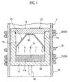
- Fig. 1 is a sectional view illustrating the outline of the apparatus of manufacturing a silicon carbide single crystal according to the embodiment of the present invention.
- the graphite crucible 10 includes a crucible main body 11, a cover member 12, and a guide member 70, and is fixed to the inside of the quartz tube 20 in a movable manner by a support rod 40.
- a sublimation material 50 is a powdery silicon carbide material including silicon carbide. If the inside of the graphite crucible 10 reaches predetermined temperature and pressure conditions, the sublimation material 50 is sublimated to become raw material gas G and the raw material gas G is recrystallized and grown on the seed crystal 60, resulting in the formation of a silicon carbide single crystal.
- the height position of the graphite crucible 10 is changed by moving the support rod 40, so that the sublimation material 50 accommodated in the bottom portion 11a of the crucible main body 11 can be made corresponding to the height position of the first induction heating coil 31, and the seed crystal 60 supported to the cover member 12 can be made corresponding to the height position of the second induction heating coil 32.
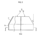
- Fig. 2 is a side view of a partial section of the guide member in Fig. 1 when viewed from the side.
- Fig. 3 is a plan view of the guide member in Fig. 2 when viewed from the top.
- the guide member 70 As illustrated in Fig. 2 , the guide member 70 according to the present embodiment has an approximately cylindrical shape, and includes an inclined portion 71 arranged at the upper side and a vertical wall portion 72 arranged at the lower side, which are integrally formed with each other.
- the guide member 70 is made of graphite,
- the inner side surface 11c of the crucible main body 11 illustrated in Fig. 1 has a cylindrical shape, and the inner diameter of the inner side surface 11c is slightly larger than the outer diameter D2 of the vertical wall portion 72. Therefore, the guide member 70 is efficiently fitted with the inner side surface 11c of the crucible main body 11.
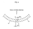
- Fig. 4 is a partial enlarged view of the section taken along line A-A of Fig. 2 .
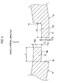
- Fig. 5 is an enlarged sectional view illustrating the state in which the first divided body is separated from the second divided body.
- the first protrusion 76 is provided at the circumferential front end thereof with a protrusion end surface 76a.
- the first protrusion 76 is provided at the radial outside thereof with a protrusion outer peripheral surface 76b.
- the radial length (thickness) of the protrusion end surface 76a is set to T1 and the circumferential length of the protrusion outer peripheral surface 76b is set to L1.
- the first protrusion 76 is provided at the radial outside thereof with a radial outside end surface 78 which extends outward in the radial direction and is connected to the protrusion outer peripheral surface 76b.
- the second protrusion 77 is provided at the circumferential front end thereof with a protrusion end surface 77a.
- the second protrusion 77 is provided at the radial inside thereof with a protrusion inner peripheral surface 77b.
- the radial length (thickness) of the protrusion end surface 77a is set to T2 and the circumferential length of the protrusion inner peripheral surface 77b is set to L2.
- the second protrusion 77 is provided at the radial inside thereof with a radially-internal end surface 79 which extends inward in the radial direction and is connected to the protrusion inner peripheral surface 77b.
- the first divided body 74 is engaged with the second divided body 75 in the state in which the protrusion outer peripheral surface 76b is brought into contact with the protrusion inner peripheral surface 77b, thereby forming the guide member 70. Further, as illustrated in Fig. 4 , the first divided body 74 is allowed to circumferentially separate from or approach the second divided body 75, so that it is possible to appropriately adjust the outer peripheral gap G (ou) and the inner peripheral gap G (in).
- the sublimation material 50 including silicon carbide is accommodated in the crucible main body 11, and the seed crystal 60 is fixed to the rear surface of the cover member 12.
- a current is allowed to flow through the first induction heating coil 31, the second induction heating coil 32, and the interference preventive coil 33 to heat and sublimate the sublimation material 50, thereby generating the raw material gas G.
- the raw material gas G rises and is recrystallized on the seed crystal 60 while being guided by the cylindrical guide member 70, so that the seed crystal 60 is grown into a silicon carbide single crystal.
- the grown silicon carbide single crystal and the guide member 70 are taken off, and the first divided body 74 and the second divided body 75 are separated from the silicon carbide single crystal.
- the taken silicon carbide single crystal is subject to peripheral grinding machining, for example, in order to obtain a desired size and a slicing process for cutting a semiconductor wafer, thereby manufacturing a semiconductor wafer.
- the apparatus of manufacturing a silicon carbide single crystal 1 includes the crucible main body 11, which is opened at the top and accommodates the sublimation material 50 in the bottom portion 11a, the cover member 12, which covers the upper opening 11b of the crucible main body 11 and is provided on the rear surface thereof with the seed crystal 60, and the cylindrical guide member 70 which is provided in the crucible main body 11 to guide the growth of a silicon carbide single crystal when the seed crystal 60 is grown to become the silicon carbide single crystal, wherein the guide member 70 includes a plurality of divided bodies, that is, the first divided body 74 and the second divided body 75.
- the gaps G (ou) and G (in) are provided between the first divided body 74 and the second divided body 75.
- the method of manufacturing a silicon carbide single crystal includes a first step of generating the raw material gas G by heating and sublimating the sublimation material 50 including silicon carbide and accommodated in the crucible main body 11, a second step in which the seed crystal 60 receiving the raw material gas G via the guide member 70 including the first divided body 74 and the second divided body 75 is grown into a silicon carbide single crystal while being guided by the guide member 70, and a third step of taking off the grown silicon carbide single crystal after separating the first divided body 74 and the second divided body 75 from the grown silicon carbide single crystal.
- the first divided body 74 is separable from the second divided body 75, it is possible to more easily take the single crystal off from the guide member 70 and to further prevent the occurrence of the damage (e.g., a crack) of the single crystal.
- the guide member 70 is divided into two, that is, the first divided body 74 and the second divided body 75.
- the guide member 70 may be divided into three or more divided bodies, and respective divided bodies may be detachably coupled to one another.
- the protrusion outer peripheral surface 76b of the first protrusion 76 is brought into contact with the protrusion inner peripheral surface 77b of the second protrusion 77.
- the protrusion outer peripheral surface 76b and the protrusion inner peripheral surface 77b may be separated from each other in the radial direction and a gap may be provided to pass through between the first divided body 74 and the second divided body 75. In such a case, the raw material gas G enters the interior of the guide member 70 through the through gap.
- the manufacturing apparatuses according to the example used the guide member 70 illustrated in Fig. 1 and the manufacturing apparatuses according to the conventional example used a single-piece guide member instead of a divided type guide member.
- the sublimation material 50 was contained in the bottom portion 11a of the crucible main body 11 and the seed crystal 60 was attached to the rear surface of the cover member 12.
- a current was allowed to flow through the first induction heating coil 31, the second induction heating coil 32, and the interference preventive coil 33 to heat the sublimation material 50 up to about 2112°C for sublimation, thereby generating the raw material gas G.
- the pressure in the crucible 10 was held to 1 Torr by argon gas.
- the raw material gas G rose and was collected to the seed crystal 60 while being guided by the cylindrical guide member 70. Since the seed crystal 60 was heated to the temperature of 2012°C which was lower than the heating temperature of the sublimation material 50, a silicon carbide single crystal was recrystallized on the seed crystal 60 and was grown. The grown silicon carbide single crystal and the guide member 70 were taken off, and the first divided body 74 and the second divided body 75 were taken off after separating them from the grown silicon carbide single crystal.
- the first divided body 74 and the second divided body 75 could be taken off from the completely grown single crystal, and a crack of the single crystal was prevented from occurring when taking off the guide member 70.
- the present invention since it is possible to divided the guide member when taking the completely grown single crystal off from the guide member, and to take the single crystal off from the guide member without giving the damage (e.g., a crack) to the single crystal, the present invention can be applied to an apparatus of manufacturing a sublimation recrystallization type silicon carbide single crystal.
Landscapes
- Chemical & Material Sciences (AREA)
- Engineering & Computer Science (AREA)
- Crystallography & Structural Chemistry (AREA)
- Materials Engineering (AREA)
- Metallurgy (AREA)
- Organic Chemistry (AREA)
- Inorganic Chemistry (AREA)
- Crystals, And After-Treatments Of Crystals (AREA)
Abstract
Description
- The present invention relates to an apparatus of manufacturing a silicon carbide single crystal by using a sublimation recrystallization method and a method of manufacturing a silicon carbide single crystal.
- Since a silicon carbide single crystal has better physical properties as compared with a generally used silicon single crystal and can be used for significantly improving the performance of an LED, a semiconductor device and the like, the silicon carbide single crystal is significantly expected as the next generation material. There has been disclosed an apparatus of manufacturing a silicon carbide single crystal (hereinafter, referred to as a single crystal, where appropriate) using a seed crystal and a sublimation material, which include silicon carbide. In general, the manufacturing apparatus includes a crucible main body for accommodating a powdery sublimation material including silicon carbide in the bottom portion thereof, a cover member for covering the upper opening of the crucible main body and provided on the rear surface thereof with a seed crystal including silicon carbide, and a cylindrical guide member provided to the inside of the crucible main body to guide a grown crystal when the seed crystal is grown (see
- Patent Document 1:
JP-A-2004-224663 Fig, 1 ) - However, in the above-mentioned conventional art, since a grown single crystal is attached to the guide member, a crack may occur from a contact portion between the single crystal and the guide member when taking the completely grown single crystal off from the guide member and performing slicing machining for the single crystal.
- Therefore, the present invention has been achieved in view of the above-described problems, and an object thereof is to provide an apparatus and a method of manufacturing a silicon carbide single crystal which prevent an occurrence of a crack from a contact portion between a single crystal and a guide member in a process of cutting the completely grown single crystal away from the guide member, even if the guide member is provided.
- The present invention for solving the above-mentioned problems has the following characteristics.
- First, a feature of the present invention is summarized as an apparatus of manufacturing a silicon carbide single crystal, including: a crucible main body (crucible main body 11) which is opened at a top and accommodates a sublimation material (sublimation material 50) in a bottom portion (
bottom portion 11a); a cover member (cover member 12) which covers an upper opening (upper opening 11b) of the crucible main body and is provided on a rear surface of the cover member with a seed crystal (seed crystal 60); and a cylindrical guide member (guide member 70) which is provided in the crucible main body to introduce a sublimated raw material gas from the sublimation material to the seed crystal and to guide growth of the silicon carbide single crystal when the silicon carbide single crystal is grown from the seed crystal, wherein the guide member includes a plurality of divided bodies (first dividedbody 74, second divided body 75). Consequently, since it has only to separate a plurality of divided bodies from each other when taking the completely grown single crystal off from the guide member, it is possible to easily take the single crystal off from the guide member and appropriately prevent the occurrence of the damage (e.g., a crack) of the single crystal. - The other feature is summarized as a gap (gap (ou), gap (in)) is provided between the divided bodies.
- The other feature is summarized as a method of manufacturing a silicon carbide single crystal, the method including: a first step of generating raw material gas by heating and sublimating a sublimation material (sublimation material 50) including silicon carbide and accommodated in a crucible main body (crucible main body 11); a second step of growing a seed crystal (seed crystal 60), which receives the raw material gas (raw material gas G) via a guide member (guide member 70) including a plurality of divided bodies (first divided
body 74, second divided body 75), into a silicon carbide single crystal while being guided by the guide member; and a third step of taking off the grown silicon carbide single crystal after separating the plurality of divided bodies from the grown silicon carbide single crystal. - According to the present invention, it is possible to provide an apparatus of manufacturing a silicon carbide single crystal capable of easily taking a single crystal off from a guide member and appropriately preventing the occurrence of the damage (e.g., a crack) of the single crystal, and to provide a method of manufacturing a silicon carbide single crystal.
-
- [
Fig. 1] Fig. 1 is a sectional view illustrating the outline of an apparatus of manufacturing a silicon carbide single crystal according to an embodiment of the present invention. - [
Fig. 2] Fig. 2 is a side view of a partial section of the guide member inFig. 1 when viewed from the side. - [
Fig. 3] Fig. 3 is a plan view of the guide member inFig. 2 when viewed from the top. - [
Fig. 4] Fig. 4 is a partial enlarged view of the section taken along line A-A ofFig. 2 . - [
Fig. 5] Fig. 5 is an enlarged sectional view illustrating the state in which a first divided body is separated from a second divided body. - Hereinafter, an embodiment of an apparatus of manufacturing a silicon carbide single crystal according to the present invention will be described with reference to the accompanying drawings. In the following drawings, the same or similar reference numerals are used to designate the same or similar parts, It will be appreciated that the drawings are schematically shown and the ratio and the like of each dimension are different from the real ones.
- Therefore, detailed dimension and the like should be determined considering the following description. Of course, among the drawings, the dimensional relationship and the ratio are different.
- An apparatus of manufacturing a silicon carbide single crystal 1 according to an embodiment of the present invention will be described with reference to
Fig. 1 . -
Fig. 1 is a sectional view illustrating the outline of the apparatus of manufacturing a silicon carbide single crystal according to the embodiment of the present invention. - As illustrated in
Fig. 1 , the apparatus of manufacturing a silicon carbide single crystal 1 includes agraphite crucible 10, aquartz tube 20 for covering at least the lateral side of thegraphite crucible 10, and aninduction heating coil 30 arranged at an outer periphery of thequartz tube 20. - The graphite crucible 10 includes a crucible
main body 11, acover member 12, and aguide member 70, and is fixed to the inside of thequartz tube 20 in a movable manner by asupport rod 40. - A sublimation material 50 (powder including silicon carbide) is accommodated in the
bottom portion 11a of the cruciblemain body 11. Thecover member 12 closes theupper opening 11b of the cruciblemain body 11 and is detachably coupled to the inner peripheral surface of the upper end portion of the cruciblemain body 11 through screw coupling. Further, aseed crystal 60 including silicon carbide is attached to the rear surface of thecover member 12. Theseed crystal 60 may be supported by mechanical coupling such as screwing or bonding using adhesive. Further, thecylindrical guide member 70 is fitted with theinner side surface 11c of the cruciblemain body 11. The upper end of theguide member 70 covers the outer periphery of theseed crystal 60 fixed to the rear surface of thecover member 12. - A
sublimation material 50 is a powdery silicon carbide material including silicon carbide. If the inside of thegraphite crucible 10 reaches predetermined temperature and pressure conditions, thesublimation material 50 is sublimated to become raw material gas G and the raw material gas G is recrystallized and grown on theseed crystal 60, resulting in the formation of a silicon carbide single crystal. - Further, the
induction heating coil 30 includes a firstinduction heating coil 31 arranged at a height position corresponding to thebottom portion 11a of the cruciblemain body 11, and a secondinduction heating coil 32 arranged at a height position corresponding to theseed crystal 60 supported to the rear surface of thecover member 12. - The height position of the
graphite crucible 10 is changed by moving thesupport rod 40, so that thesublimation material 50 accommodated in thebottom portion 11a of the cruciblemain body 11 can be made corresponding to the height position of the firstinduction heating coil 31, and theseed crystal 60 supported to thecover member 12 can be made corresponding to the height position of the secondinduction heating coil 32. - In addition, an interference
preventive coil 33 is provided between the firstinduction heating coil 31 and the secondinduction heating coil 32. A current is allowed to flow through the interferencepreventive coil 33, so that it is possible to prevent interference between a current flowing through the firstinduction heating coil 31 and a current flowing through the secondinduction heating coil 32. -
Fig. 2 is a side view of a partial section of the guide member inFig. 1 when viewed from the side.Fig. 3 is a plan view of the guide member inFig. 2 when viewed from the top. - As illustrated in
Fig. 2 , theguide member 70 according to the present embodiment has an approximately cylindrical shape, and includes aninclined portion 71 arranged at the upper side and avertical wall portion 72 arranged at the lower side, which are integrally formed with each other. Theguide member 70 is made of graphite, - As illustrated in
Fig. 2 , theinclined portion 71 has a circular truncated cone shape in side view. Thevertical wall portion 72 has a rectangular shape in side view. Further, as illustrated inFig. 3 , theinclined portion 71 is formed at the upper end thereof with acircular opening 73 in planar view. The inner diameter D1 of theopening 73 is larger than the outer diameter of the seed crystal 60 (seeFig. 1 ). - Further, the
inner side surface 11c of the cruciblemain body 11 illustrated inFig. 1 has a cylindrical shape, and the inner diameter of theinner side surface 11c is slightly larger than the outer diameter D2 of thevertical wall portion 72. Therefore, theguide member 70 is efficiently fitted with theinner side surface 11c of the cruciblemain body 11. - Further, the
guide member 70 includes a first dividedbody 74 and a second dividedbody 75, and is divided into two about the center in the radial direction. A small gap G (ou) is formed at a joint portion between the first dividedbody 74 and the second dividedbody 75 along the circumferential direction. -
Fig. 4 is a partial enlarged view of the section taken along line A-A ofFig. 2 .Fig. 5 is an enlarged sectional view illustrating the state in which the first divided body is separated from the second divided body. - As illustrated in
Figs. 4 and5 , afirst protrusion 76 is formed at the radial inside of the circumferential end of the first dividedbody 74. Asecond protrusion 77 is formed at the radial outside of the circumferential end of the second dividedbody 75. - The
first protrusion 76 is provided at the circumferential front end thereof with aprotrusion end surface 76a. Thefirst protrusion 76 is provided at the radial outside thereof with a protrusion outerperipheral surface 76b. The radial length (thickness) of theprotrusion end surface 76a is set to T1 and the circumferential length of the protrusion outerperipheral surface 76b is set to L1. Further, thefirst protrusion 76 is provided at the radial outside thereof with a radialoutside end surface 78 which extends outward in the radial direction and is connected to the protrusion outerperipheral surface 76b. - Meanwhile, the
second protrusion 77 is provided at the circumferential front end thereof with aprotrusion end surface 77a. Thesecond protrusion 77 is provided at the radial inside thereof with a protrusion innerperipheral surface 77b. The radial length (thickness) of theprotrusion end surface 77a is set to T2 and the circumferential length of the protrusion innerperipheral surface 77b is set to L2. Further, thesecond protrusion 77 is provided at the radial inside thereof with a radially-internal end surface 79 which extends inward in the radial direction and is connected to the protrusion innerperipheral surface 77b. - Consequently, the first divided
body 74 is engaged with the second dividedbody 75 in the state in which the protrusion outerperipheral surface 76b is brought into contact with the protrusion innerperipheral surface 77b, thereby forming theguide member 70. Further, as illustrated inFig. 4 , the first dividedbody 74 is allowed to circumferentially separate from or approach the second dividedbody 75, so that it is possible to appropriately adjust the outer peripheral gap G (ou) and the inner peripheral gap G (in). - Further, in the stage before single crystal growth is completed, the gap G (ou) and the gap G (in) are changed, so that it is possible to adjust an angle θ (see
Fig. 2 ) of theinclined portion 71 with respect to the vertical direction. For example, in the state in which an initial angle θ is set to 30 degrees and theseed crystal 60 is grown, the angle µ may be changed to 45 degrees at the time at which the growth height of a single crystal reaches 0.5 mm to several mm. Consequently, it is possible to expand the diameter of a single crystal without degradation in quality. - Hereinafter, a method of manufacturing a single crystal according to the present embodiment will be briefly described.
- First, in the first step, as illustrated in
Fig. 1 , thesublimation material 50 including silicon carbide is accommodated in the cruciblemain body 11, and theseed crystal 60 is fixed to the rear surface of thecover member 12. A current is allowed to flow through the firstinduction heating coil 31, the secondinduction heating coil 32, and the interferencepreventive coil 33 to heat and sublimate thesublimation material 50, thereby generating the raw material gas G. - In the second step, the raw material gas G rises and is recrystallized on the
seed crystal 60 while being guided by thecylindrical guide member 70, so that theseed crystal 60 is grown into a silicon carbide single crystal. - In the third step, the grown silicon carbide single crystal and the
guide member 70 are taken off, and the first dividedbody 74 and the second dividedbody 75 are separated from the silicon carbide single crystal. - In addition, the taken silicon carbide single crystal is subject to peripheral grinding machining, for example, in order to obtain a desired size and a slicing process for cutting a semiconductor wafer, thereby manufacturing a semiconductor wafer.
- The operation and effect according to the embodiment of the present invention will be described.
- The apparatus of manufacturing a silicon carbide single crystal 1 according to the present embodiment includes the crucible
main body 11, which is opened at the top and accommodates thesublimation material 50 in thebottom portion 11a, thecover member 12, which covers theupper opening 11b of the cruciblemain body 11 and is provided on the rear surface thereof with theseed crystal 60, and thecylindrical guide member 70 which is provided in the cruciblemain body 11 to guide the growth of a silicon carbide single crystal when theseed crystal 60 is grown to become the silicon carbide single crystal, wherein theguide member 70 includes a plurality of divided bodies, that is, the first dividedbody 74 and the second dividedbody 75. - Consequently, when taking the completely grown single crystal off from the
guide member 70, it is possible to separate the first dividedbody 74 from the second dividedbody 75, and easily take the single crystal off from theguide member 70. Thus, it is possible to appropriately prevent the occurrence of the damage (e.g., a crack) of the single crystal. - In the apparatus of manufacturing a silicon carbide single crystal 1 according to the present embodiment, the gaps G (ou) and G (in) are provided between the first divided
body 74 and the second dividedbody 75. Thus, it is possible to easily take the single crystal off from theguide member 70 by separating the first dividedbody 74 from the second dividedbody 75. Consequently, it is possible to appropriately prevent the occurrence of the damage (e.g., a crack) when taking the single crystal out from theguide member 70. - The method of manufacturing a silicon carbide single crystal according to the present embodiment includes a first step of generating the raw material gas G by heating and sublimating the
sublimation material 50 including silicon carbide and accommodated in the cruciblemain body 11, a second step in which theseed crystal 60 receiving the raw material gas G via theguide member 70 including the first dividedbody 74 and the second dividedbody 75 is grown into a silicon carbide single crystal while being guided by theguide member 70, and a third step of taking off the grown silicon carbide single crystal after separating the first dividedbody 74 and the second dividedbody 75 from the grown silicon carbide single crystal. - In this way, since the first divided
body 74 is separable from the second dividedbody 75, it is possible to more easily take the single crystal off from theguide member 70 and to further prevent the occurrence of the damage (e.g., a crack) of the single crystal. - As described above, the scope of the present invention has been disclosed through the embodiment of the present invention. However, it should be understood that those descriptions and drawings constituting a part of the present disclosure do not limit the present invention. From the present disclosure, various alternative embodiments, examples, and operational technologies will become apparent to those skilled in the art.
- For example, the
guide member 70 is divided into two, that is, the first dividedbody 74 and the second dividedbody 75. However, theguide member 70 may be divided into three or more divided bodies, and respective divided bodies may be detachably coupled to one another. - Further, in the embodiment, the protrusion outer
peripheral surface 76b of thefirst protrusion 76 is brought into contact with the protrusion innerperipheral surface 77b of thesecond protrusion 77. However, the protrusion outerperipheral surface 76b and the protrusion innerperipheral surface 77b may be separated from each other in the radial direction and a gap may be provided to pass through between the first dividedbody 74 and the second dividedbody 75. In such a case, the raw material gas G enters the interior of theguide member 70 through the through gap. - As described above, it is of course that the present invention includes various embodiments and the like not described above. Accordingly, the technical scope of the present invention is determined only by the invention elements according to the scope of claims from the viewpoint of the above explanation.
- Next, in order to clarify the effect of the present invention, experimental results performed using apparatuses of manufacturing a silicon carbide single crystal according to a conventional example and an example will be described.
- The manufacturing apparatuses according to the example used the
guide member 70 illustrated inFig. 1 and the manufacturing apparatuses according to the conventional example used a single-piece guide member instead of a divided type guide member. - In the example, first, the
sublimation material 50 was contained in thebottom portion 11a of the cruciblemain body 11 and theseed crystal 60 was attached to the rear surface of thecover member 12. A current was allowed to flow through the firstinduction heating coil 31, the secondinduction heating coil 32, and the interferencepreventive coil 33 to heat thesublimation material 50 up to about 2112°C for sublimation, thereby generating the raw material gas G. At this time, the pressure in thecrucible 10 was held to 1 Torr by argon gas. - The raw material gas G rose and was collected to the
seed crystal 60 while being guided by thecylindrical guide member 70. Since theseed crystal 60 was heated to the temperature of 2012°C which was lower than the heating temperature of thesublimation material 50, a silicon carbide single crystal was recrystallized on theseed crystal 60 and was grown. The grown silicon carbide single crystal and theguide member 70 were taken off, and the first dividedbody 74 and the second dividedbody 75 were taken off after separating them from the grown silicon carbide single crystal. - As described above, in the manufacturing apparatuses according to the example, the first divided
body 74 and the second dividedbody 75 could be taken off from the completely grown single crystal, and a crack of the single crystal was prevented from occurring when taking off theguide member 70. - Meanwhile, in the manufacturing apparatuses according to the conventional example, since the guide member was formed in a single-piece, a crack occurred in the completely grown single crystal when taking the guide member off from the completely grown single crystal.
- It is noted that the entire contents of Japanese Patent Application No.
2009-100295 (filed on April 16, 2009 - According to the present invention, since it is possible to divided the guide member when taking the completely grown single crystal off from the guide member, and to take the single crystal off from the guide member without giving the damage (e.g., a crack) to the single crystal, the present invention can be applied to an apparatus of manufacturing a sublimation recrystallization type silicon carbide single crystal.
- 1 ... Manufacturing apparatus, 10 ... Graphite crucible, 11 ... Crucible main body, 11a ... Bottom portion, 11b ... Upper opening, 11c ... Inner side surface, 12 ... Cover member, 30 ... Induction heating coil, 31 ... First induction heating coil, 32 ... Second induction heating coil, 33 ... Interference preventive coil, 40 ... Support rod, 50 ... Sublimation material, 60 ... Seed crystal, 70 ... Guide member, 74 ... First divided body, 75 ... Second divided body, G ... Raw material gas, G(ou), G(in) ... Gap
Claims (3)
- An apparatus of manufacturing a silicon carbide single crystal, comprising:a crucible main body which is opened at a top and accommodates a sublimation material in a bottom portion;a cover member which covers an upper opening of the crucible main body and is provided on a rear surface thereof with a seed crystal; anda cylindrical guide member which is provided in the crucible main body to introduce a sublimated raw material gas from the sublimation material to the seed crystal and to guide growth of the silicon carbide single crystal when the silicon carbide single crystal is grown from the seed crystal, whereinthe guide member includes a plurality of divided bodies.
- The apparatus of manufacturing a silicon carbide single crystal according to claim 1, wherein a gap is provided between the divided bodies.
- A method of manufacturing a silicon carbide single crystal, the method comprising:a first step of generating raw material gas by heating and sublimating a sublimation material including silicon carbide and accommodated in a crucible main body;a second step of growing a seed crystal, which receives the raw material gas via a guide member including a plurality of divided bodies, into a silicon carbide single crystal while being guided by the guide member; anda third step of taking off the grown silicon carbide single crystal after separating the plurality of divided bodies from the grown silicon carbide single crystal.
Applications Claiming Priority (2)
| Application Number | Priority Date | Filing Date | Title |
|---|---|---|---|
| JP2009100295A JP5432573B2 (en) | 2009-04-16 | 2009-04-16 | Silicon carbide single crystal manufacturing apparatus and silicon carbide single crystal manufacturing method |
| PCT/JP2010/054860 WO2010119749A1 (en) | 2009-04-16 | 2010-03-19 | Apparatus for producing silicon carbide single crystal and method for producing silicon carbide single crystal |
Publications (2)
| Publication Number | Publication Date |
|---|---|
| EP2420598A1 true EP2420598A1 (en) | 2012-02-22 |
| EP2420598A4 EP2420598A4 (en) | 2013-05-01 |
Family
ID=42982415
Family Applications (1)
| Application Number | Title | Priority Date | Filing Date |
|---|---|---|---|
| EP10764335.5A Withdrawn EP2420598A4 (en) | 2009-04-16 | 2010-03-19 | Apparatus for producing silicon carbide single crystal and method for producing silicon carbide single crystal |
Country Status (5)
| Country | Link |
|---|---|
| US (1) | US20120060749A1 (en) |
| EP (1) | EP2420598A4 (en) |
| JP (1) | JP5432573B2 (en) |
| CN (1) | CN102395716A (en) |
| WO (1) | WO2010119749A1 (en) |
Cited By (2)
| Publication number | Priority date | Publication date | Assignee | Title |
|---|---|---|---|---|
| CN112899782A (en) * | 2021-01-18 | 2021-06-04 | 河南城建学院 | Crystal preparation device |
| CN113458905A (en) * | 2020-03-31 | 2021-10-01 | 株式会社电装 | Method for producing silicon carbide wafer, method for producing semiconductor substrate, and method for producing silicon carbide semiconductor device |
Families Citing this family (12)
| Publication number | Priority date | Publication date | Assignee | Title |
|---|---|---|---|---|
| DE102015212323A1 (en) | 2014-07-04 | 2016-01-07 | Sumitomo Electric Industries, Ltd. | Crucible and process for producing a single crystal |
| JP2016098157A (en) * | 2014-11-25 | 2016-05-30 | 住友電気工業株式会社 | Method for producing silicon carbide single crystal |
| CN105040103A (en) * | 2015-06-25 | 2015-11-11 | 江苏艾科勒科技有限公司 | Growing device for high-quality silicon carbide crystals |
| JP6694807B2 (en) | 2016-12-26 | 2020-05-20 | 昭和電工株式会社 | Method for producing silicon carbide single crystal |
| JP6881365B2 (en) * | 2018-03-16 | 2021-06-02 | 信越半導体株式会社 | Silicon Carbide Single Crystal Manufacturing Method and Equipment |
| JP7076279B2 (en) * | 2018-04-26 | 2022-05-27 | 昭和電工株式会社 | SiC single crystal growth device and method for growing SiC single crystal |
| KR102202447B1 (en) * | 2018-12-18 | 2021-01-14 | 주식회사 포스코 | Growth device for silicon carbide single crystal |
| CN111058088B (en) * | 2019-12-24 | 2021-03-23 | 山东天岳先进科技股份有限公司 | Crystal growth furnace for preparing single crystal by PVT method and application thereof |
| CN111349966A (en) * | 2020-03-26 | 2020-06-30 | 哈尔滨科友半导体产业装备与技术研究院有限公司 | Size-adjustable combined crucible thermal field |
| AT524251B1 (en) * | 2020-09-28 | 2023-04-15 | Ebner Ind Ofenbau | Apparatus for growing single crystals |
| CN115821372B (en) * | 2022-11-29 | 2026-01-13 | 湖南三安半导体有限责任公司 | Crystal growth apparatus |
| CN120330875B (en) * | 2025-04-30 | 2026-01-30 | 通威微电子有限公司 | Silicon carbide crystal growing furnace and silicon carbide crystal growing method |
Family Cites Families (7)
| Publication number | Priority date | Publication date | Assignee | Title |
|---|---|---|---|---|
| JP3843615B2 (en) * | 1998-07-30 | 2006-11-08 | 株式会社デンソー | Single crystal growth equipment |
| JP3719866B2 (en) * | 1999-01-28 | 2005-11-24 | 株式会社シクスオン | Crucible, crystal growth apparatus, and crystal growth method |
| JP4102876B2 (en) | 2003-01-27 | 2008-06-18 | 独立行政法人産業技術総合研究所 | Single crystal growth equipment |
| JP4150642B2 (en) * | 2003-08-04 | 2008-09-17 | 株式会社デンソー | Single crystal growth method and growth apparatus |
| JP4926655B2 (en) * | 2006-11-02 | 2012-05-09 | 新日本製鐵株式会社 | Graphite crucible for silicon carbide single crystal growth and silicon carbide single crystal manufacturing apparatus |
| JP2009100295A (en) | 2007-10-17 | 2009-05-07 | Olympus Imaging Corp | Electronic camera |
| JP5143139B2 (en) * | 2007-11-08 | 2013-02-13 | パナソニック株式会社 | Single crystal growth equipment |
-
2009
- 2009-04-16 JP JP2009100295A patent/JP5432573B2/en not_active Expired - Fee Related
-
2010
- 2010-03-19 CN CN2010800171310A patent/CN102395716A/en active Pending
- 2010-03-19 US US13/264,624 patent/US20120060749A1/en not_active Abandoned
- 2010-03-19 EP EP10764335.5A patent/EP2420598A4/en not_active Withdrawn
- 2010-03-19 WO PCT/JP2010/054860 patent/WO2010119749A1/en not_active Ceased
Cited By (5)
| Publication number | Priority date | Publication date | Assignee | Title |
|---|---|---|---|---|
| CN113458905A (en) * | 2020-03-31 | 2021-10-01 | 株式会社电装 | Method for producing silicon carbide wafer, method for producing semiconductor substrate, and method for producing silicon carbide semiconductor device |
| EP3889324A1 (en) * | 2020-03-31 | 2021-10-06 | Denso Corporation | Production method of silicon carbide wafer, production method of semiconductor substrate, and production method of silicon carbide semiconductor device |
| US11795576B2 (en) | 2020-03-31 | 2023-10-24 | Denso Corporation | Production method of silicon carbide wafer, production method of semiconductor substrate, and production method of silicon carbide semiconductor device |
| CN112899782A (en) * | 2021-01-18 | 2021-06-04 | 河南城建学院 | Crystal preparation device |
| CN112899782B (en) * | 2021-01-18 | 2022-03-11 | 河南城建学院 | A crystal preparation device |
Also Published As
| Publication number | Publication date |
|---|---|
| US20120060749A1 (en) | 2012-03-15 |
| JP2010248039A (en) | 2010-11-04 |
| EP2420598A4 (en) | 2013-05-01 |
| WO2010119749A1 (en) | 2010-10-21 |
| JP5432573B2 (en) | 2014-03-05 |
| CN102395716A (en) | 2012-03-28 |
Similar Documents
| Publication | Publication Date | Title |
|---|---|---|
| US20120060749A1 (en) | Apparatus of manufacturing silicon carbide single crystal and method of manufacturing silicon carbide single crystal | |
| EP2287367B1 (en) | Single crystal manufacturing device and manufacturing method | |
| EP2524978B1 (en) | Apparatus for producing silicon carbide single crystal | |
| EP2441861B1 (en) | Device for producing silicon carbide single crystals | |
| EP2365110A1 (en) | Apparatus and method for producing silicon carbide single crystal | |
| US10988857B2 (en) | SiC single crystal growth apparatus containing movable heat-insulating material and growth method of SiC single crystal using the same | |
| CN111304745A (en) | Ingot preparation device and preparation method of silicon carbide single crystal ingot | |
| CN110878427A (en) | single crystal growth method | |
| CN109423689B (en) | Heat shield member, single crystal pulling apparatus, and single crystal pulling method | |
| KR20130083654A (en) | Growing apparatus for single crystal | |
| JP2012036035A (en) | Method for manufacturing silicon carbide single crystal | |
| JP2012171800A (en) | Method and apparatus for producing silicon carbide single crystal | |
| EP4174224A1 (en) | Method for producing sic crystals | |
| JP5087489B2 (en) | Silicon carbide single crystal manufacturing apparatus and silicon carbide single crystal manufacturing method | |
| RU2562484C1 (en) | PROCEDURE FOR MONOCRYSTAL SiC PRODUCTION | |
| US11815437B2 (en) | Method of acquiring sample for evaluation of SiC single crystal | |
| US7491270B2 (en) | Heat shield member and single crystal pulling device | |
| JP5831339B2 (en) | Method for producing silicon carbide single crystal | |
| JP6052051B2 (en) | Silicon carbide single crystal manufacturing equipment | |
| JP2010241619A (en) | Production method of silicon carbide single crystal | |
| JP4206809B2 (en) | Heat shielding member and single crystal pulling apparatus using the same | |
| JP2010163335A (en) | Manufacturing apparatus of silicon carbide single crystal, and manufacturing method of silicon carbide single crystal | |
| KR101649543B1 (en) | Reverse sublimation apparatus for single crystal growth | |
| JP2011184209A (en) | Apparatus for producing single crystal, method for fixing seed crystal, and method for producing silicon carbide single crystal | |
| KR101398048B1 (en) | Growing apparatus for single crystal |
Legal Events
| Date | Code | Title | Description |
|---|---|---|---|
| PUAI | Public reference made under article 153(3) epc to a published international application that has entered the european phase |
Free format text: ORIGINAL CODE: 0009012 |
|
| 17P | Request for examination filed |
Effective date: 20111021 |
|
| AK | Designated contracting states |
Kind code of ref document: A1 Designated state(s): AT BE BG CH CY CZ DE DK EE ES FI FR GB GR HR HU IE IS IT LI LT LU LV MC MK MT NL NO PL PT RO SE SI SK SM TR |
|
| DAX | Request for extension of the european patent (deleted) | ||
| A4 | Supplementary search report drawn up and despatched |
Effective date: 20130402 |
|
| RIC1 | Information provided on ipc code assigned before grant |
Ipc: C30B 29/36 20060101AFI20130325BHEP Ipc: C30B 23/00 20060101ALI20130325BHEP |
|
| GRAP | Despatch of communication of intention to grant a patent |
Free format text: ORIGINAL CODE: EPIDOSNIGR1 |
|
| INTG | Intention to grant announced |
Effective date: 20160304 |
|
| STAA | Information on the status of an ep patent application or granted ep patent |
Free format text: STATUS: THE APPLICATION IS DEEMED TO BE WITHDRAWN |
|
| 18D | Application deemed to be withdrawn |
Effective date: 20160715 |