EP2418700A2 - Light emitting device package and lighting system having the same - Google Patents
Light emitting device package and lighting system having the same Download PDFInfo
- Publication number
- EP2418700A2 EP2418700A2 EP11176899A EP11176899A EP2418700A2 EP 2418700 A2 EP2418700 A2 EP 2418700A2 EP 11176899 A EP11176899 A EP 11176899A EP 11176899 A EP11176899 A EP 11176899A EP 2418700 A2 EP2418700 A2 EP 2418700A2
- Authority
- EP
- European Patent Office
- Prior art keywords
- light emitting
- metal layer
- layer
- metal layers
- disposed
- Prior art date
- Legal status (The legal status is an assumption and is not a legal conclusion. Google has not performed a legal analysis and makes no representation as to the accuracy of the status listed.)
- Granted
Links
Images










Classifications
-
- H—ELECTRICITY
- H10—SEMICONDUCTOR DEVICES; ELECTRIC SOLID-STATE DEVICES NOT OTHERWISE PROVIDED FOR
- H10H—INORGANIC LIGHT-EMITTING SEMICONDUCTOR DEVICES HAVING POTENTIAL BARRIERS
- H10H20/00—Individual inorganic light-emitting semiconductor devices having potential barriers, e.g. light-emitting diodes [LED]
- H10H20/80—Constructional details
- H10H20/85—Packages
- H10H20/855—Optical field-shaping means, e.g. lenses
- H10H20/856—Reflecting means
-
- H—ELECTRICITY
- H10—SEMICONDUCTOR DEVICES; ELECTRIC SOLID-STATE DEVICES NOT OTHERWISE PROVIDED FOR
- H10H—INORGANIC LIGHT-EMITTING SEMICONDUCTOR DEVICES HAVING POTENTIAL BARRIERS
- H10H20/00—Individual inorganic light-emitting semiconductor devices having potential barriers, e.g. light-emitting diodes [LED]
- H10H20/80—Constructional details
- H10H20/85—Packages
- H10H20/8506—Containers
-
- H—ELECTRICITY
- H10—SEMICONDUCTOR DEVICES; ELECTRIC SOLID-STATE DEVICES NOT OTHERWISE PROVIDED FOR
- H10H—INORGANIC LIGHT-EMITTING SEMICONDUCTOR DEVICES HAVING POTENTIAL BARRIERS
- H10H20/00—Individual inorganic light-emitting semiconductor devices having potential barriers, e.g. light-emitting diodes [LED]
- H10H20/01—Manufacture or treatment
- H10H20/036—Manufacture or treatment of packages
-
- H—ELECTRICITY
- H10—SEMICONDUCTOR DEVICES; ELECTRIC SOLID-STATE DEVICES NOT OTHERWISE PROVIDED FOR
- H10H—INORGANIC LIGHT-EMITTING SEMICONDUCTOR DEVICES HAVING POTENTIAL BARRIERS
- H10H20/00—Individual inorganic light-emitting semiconductor devices having potential barriers, e.g. light-emitting diodes [LED]
- H10H20/80—Constructional details
- H10H20/85—Packages
- H10H20/851—Wavelength conversion means
- H10H20/8514—Wavelength conversion means characterised by their shape, e.g. plate or foil
-
- H—ELECTRICITY
- H10—SEMICONDUCTOR DEVICES; ELECTRIC SOLID-STATE DEVICES NOT OTHERWISE PROVIDED FOR
- H10H—INORGANIC LIGHT-EMITTING SEMICONDUCTOR DEVICES HAVING POTENTIAL BARRIERS
- H10H20/00—Individual inorganic light-emitting semiconductor devices having potential barriers, e.g. light-emitting diodes [LED]
- H10H20/80—Constructional details
- H10H20/85—Packages
- H10H20/851—Wavelength conversion means
- H10H20/8515—Wavelength conversion means not being in contact with the bodies
-
- H—ELECTRICITY
- H10—SEMICONDUCTOR DEVICES; ELECTRIC SOLID-STATE DEVICES NOT OTHERWISE PROVIDED FOR
- H10H—INORGANIC LIGHT-EMITTING SEMICONDUCTOR DEVICES HAVING POTENTIAL BARRIERS
- H10H20/00—Individual inorganic light-emitting semiconductor devices having potential barriers, e.g. light-emitting diodes [LED]
- H10H20/80—Constructional details
- H10H20/85—Packages
- H10H20/855—Optical field-shaping means, e.g. lenses
-
- H—ELECTRICITY
- H10—SEMICONDUCTOR DEVICES; ELECTRIC SOLID-STATE DEVICES NOT OTHERWISE PROVIDED FOR
- H10H—INORGANIC LIGHT-EMITTING SEMICONDUCTOR DEVICES HAVING POTENTIAL BARRIERS
- H10H20/00—Individual inorganic light-emitting semiconductor devices having potential barriers, e.g. light-emitting diodes [LED]
- H10H20/80—Constructional details
- H10H20/85—Packages
- H10H20/857—Interconnections, e.g. lead-frames, bond wires or solder balls
-
- H—ELECTRICITY
- H10—SEMICONDUCTOR DEVICES; ELECTRIC SOLID-STATE DEVICES NOT OTHERWISE PROVIDED FOR
- H10H—INORGANIC LIGHT-EMITTING SEMICONDUCTOR DEVICES HAVING POTENTIAL BARRIERS
- H10H20/00—Individual inorganic light-emitting semiconductor devices having potential barriers, e.g. light-emitting diodes [LED]
- H10H20/80—Constructional details
- H10H20/85—Packages
- H10H20/858—Means for heat extraction or cooling
- H10H20/8582—Means for heat extraction or cooling characterised by their shape
-
- H—ELECTRICITY
- H10—SEMICONDUCTOR DEVICES; ELECTRIC SOLID-STATE DEVICES NOT OTHERWISE PROVIDED FOR
- H10H—INORGANIC LIGHT-EMITTING SEMICONDUCTOR DEVICES HAVING POTENTIAL BARRIERS
- H10H20/00—Individual inorganic light-emitting semiconductor devices having potential barriers, e.g. light-emitting diodes [LED]
- H10H20/80—Constructional details
- H10H20/85—Packages
- H10H20/858—Means for heat extraction or cooling
- H10H20/8585—Means for heat extraction or cooling being an interconnection
-
- H—ELECTRICITY
- H10—SEMICONDUCTOR DEVICES; ELECTRIC SOLID-STATE DEVICES NOT OTHERWISE PROVIDED FOR
- H10H—INORGANIC LIGHT-EMITTING SEMICONDUCTOR DEVICES HAVING POTENTIAL BARRIERS
- H10H20/00—Individual inorganic light-emitting semiconductor devices having potential barriers, e.g. light-emitting diodes [LED]
- H10H20/80—Constructional details
- H10H20/882—Scattering means
-
- H—ELECTRICITY
- H10—SEMICONDUCTOR DEVICES; ELECTRIC SOLID-STATE DEVICES NOT OTHERWISE PROVIDED FOR
- H10W—GENERIC PACKAGES, INTERCONNECTIONS, CONNECTORS OR OTHER CONSTRUCTIONAL DETAILS OF DEVICES COVERED BY CLASS H10
- H10W90/00—Package configurations
- H10W90/701—Package configurations characterised by the relative positions of pads or connectors relative to package parts
- H10W90/721—Package configurations characterised by the relative positions of pads or connectors relative to package parts of bump connectors
- H10W90/726—Package configurations characterised by the relative positions of pads or connectors relative to package parts of bump connectors between a chip and a stacked lead frame, conducting package substrate or heat sink
Definitions
- Embodiments provide a light emitting device in which a resin layer is disposed around a light emitting chip and a guide member is disposed around the resin layer and a lighting system having the same.
- Embodiments provide a light emitting device including: an adhesive layer between the plurality of metal layers and the first insulation film and the second insulation film.
- Fig. 2 is a side sectional view taken along line A-A of Fig. 1 .
- Figs. 11 and 12 are side sectional views of a light emitting device according to second and third embodiments.
- Each of the metal layers 11 and 13 may have a thickness of about 15 ⁇ m to about 300 ⁇ m, and preferably, about 15 ⁇ m to about 50 ⁇ m. Also, the metal layers 11 and 13 may serve as a support frame for supporting the entire light emitting device and a heat-dissipating member for conducting heat generated from the light emitting chip 41. In outer areas of the metal layers 11 and 13, a length Y1 of a first direction Y and a length X1 of a second direction X perpendicular to the first direction Y may vary according to a size of the light emitting device 100.
- each of the insulation films 21 and 23 may include a light-transmitting or non-light-transmitting film.
- each of the insulation films 21 and 23 may include a polyimide (PI) film, a polyethylene terephthalate (PET) film, an ethylene vinyl acetate (EVA) film, a polyethylene naphthalate (PEN) film, a triacetyl cellulose (TAC) film, a polyamide imide (PAI) film, a polyether ether ketone (PEEK) film, a perfluoroalkoxy (PFA) film, a polyphenylene sulfide (PPS) film, and resin films (PE, PP, and PET).
- PI polyimide
- PET polyethylene terephthalate
- EVA ethylene vinyl acetate
- PEN polyethylene naphthalate
- TAC triacetyl cellulose
- PAI polyamide imide
- PEEK polyether ether ketone
- PFA perfluor
- Each of the insulation films 21 and 23 may be formed of a material having a predetermined reflective index, e.g., a reflective index of about 30% or more.
- the reflection characteristics of the insulation films 21 and 23 may improve surface reflection efficiency within the light emitting device 100.
- One of the plurality of opened areas A1 and A2, e.g., the second opened area S2 may have a minimum width of about 60 ⁇ m.
- the bonding of a second wire 52 may be interrupted.
- the second opened area A2 may have a width of at least 60 ⁇ m.
- the first opened area A1 may have a width enough to mount the light emitting chip 41.
- the first opened area A1 may have a width wider than that of the second opened area A2.
- the first opened area A1 is described as an area on which the light emitting chip 41 is mounted and the second opened area A2 is described as an area to which a second wire 52 is bonded, the present disclosure is not limited thereto.
- the first opened area A1 may be an area to which a second wire 52 is bonded and the second opened area A2 may be an area on which the light emitting chip 41 is mounted.
- the first insulation film 21 may have a constant width W1. Alternatively, the first insulation film 21 may have widths different from each other. The first insulation film 21 may have a width W1 of several ten ⁇ m or more.
- the second insulation film 23 may have a constant width W2. Alternatively, the first insulation film 23 may have widths different from each other. The second insulation film 23 may have a width W2 greater than an interval G1 between the metal layers 11 and 13. For example, the second insulation film 23 may have a width of about 20 ⁇ m or more. The width W1 of the first insulation film 21 may be equal to or different from the W2 of the second insulation film 23.
- the second opened area A2 may have a minimum width of about 60 ⁇ m.
- the second opened area A2 may have a width at which a bonding process of a wire is not interrupted.
- the first opened area A1 may have a width enough to mount a light emitting chip.
- the first opened area A1 may have a width wider than that of the second opened area A2.
- the first opened area A1 is described as an area on which the light emitting chip is mounted and the second opened area A2 is described as an area to which the wire is bonded, the present disclosure is not limited thereto.
- the first opened area A1 may be an area to which the wire is bonded and the second opened area A2 may be an area on which the light emitting chip is mounted.
- Fig. 11 is a side sectional view of a light emitting device according to a second embodiment.
- a resin layer 61 is disposed on the first metal layer 11 and the second metal layer 13.
- the resin layer 61 may be injection-molded in a predetermined shape through a transfer molding method. According to the transfer molding method, a liquid resin is filled into a frame having a predetermined shape and then cured so that the resin layer 61 having a desired shape may be formed.
- the resin layer 61 may have a cylindrical shape, a polygonal column shape, or uneven surface shape, but is not limited thereto.
- An outer surface of the resin layer 61 may be spaced a predetermined interval T3 inward from an outer part of the first metal layer 11 or the second metal layer 13. Accordingly, the outer top surfaces of the first metal layer 11 and the second metal layer 13 may be exposed.
- the interval T3 may be about 1 ⁇ m or more.
- the resin layer 63 is disposed on top surfaces of the metal layers 11 and 13.
- An insulation film 21 is disposed around the resin layer 63.
- the resin layer 63 may have a convex lens shape.
- a guide member 31 or a reflective material may be further disposed around the resin layer 63, but is not limited thereto.
- a spacer 18 is disposed on a separation part 17 between the first metal layer 11 and the second metal layer 13.
- the spacer 18 is disposed between the first metal layer 11 and the second metal layer 13 and is formed of an insulation material.
- the spacer 18 adheres between the first metal layer 11 and the second metal layer 13.
- the spacer 18 may space the first metal layer 11 from the second metal layer 13 to prevent the first and second metal layers 11 and 13 from being electrically short-circuited with each other.
- the spacer 18 may be formed of at least one of SiO 2 , SiO x , SiO x N y , Si 3 N 4 , Al 2 O 3 , and TiO 2 .
- the resin layer 63 may have a convex hemispherical shape. Also, a concave part 63B having a predetermined depth is defined in a center of the resin layer 63.
- the concave part 63B may have a horn shape or a hemispherical shape.
- a reflective material 72 may be disposed within the concave part 63B.
- the reflective material 72 may include a metal oxide.
- the reflective material 72 may form at least one layer formed of a material such as TiO 2 or/and SiO 2 to reflect incident light into a side direction.
- the resin layer 63 and the reflective material 72 may have refractive indexes different from each other.
- the reflective material 72 may have a refractive index greater than that of the resin layer 63.
- the resin layer 63 may reflect light of a center direction toward the side direction to uniformly provide orientation angle distribution of the light.
- the second guide member 37C may be disposed on top and inner surfaces of the second insulation film 23 to contact the top surface of the first metal layer 11.
- the second guide member 37B may be connected to the first guide member 37A and may be separated from the third guide member 37C.
- the second guide member 37C may be physically spaced from the second metal layer 13.
- the first to third guide members 37A, 37C, and 37B may be formed of the same material as or materials different from each other, but is not limited thereto.
- the first to third guide members 37A, 37C, and 37B may be formed of a metal material or an insulation material as another example.
- the first light emitting chip 41A may be electrically connected to the first metal layer 12A and the second metal layer 12B through a first wire 51A and a second wire 51B, respectively.
- the second light emitting chip 41B may be electrically connected to the second metal layer 12B and the third metal layer 12C through a third wire 51C and a fourth wire 51D, respectively.
- the first insulation film 21 may be disposed on the outer part B1 of the metal layers 11 and 13.
- the guide member 31 may be disposed on the firs insulation film 21.
- the bottom cover 1011 may be formed of a metal material or a resin material. Also, the bottom cover 1011 may be manufactured using a press molding process or an extrusion molding process. The bottom cover 1011 may be formed of a metal or non-metal material having superior heat conductivity, but is not limited thereto.
- the substrate 1120 and the light emitting device 100 may be defined as a light emitting module 1060.
- the bottom cover 1152, at least one light emitting module 1060, the optical member 1154 may be defined as the light unit.
Landscapes
- Led Device Packages (AREA)
- Planar Illumination Modules (AREA)
- Non-Portable Lighting Devices Or Systems Thereof (AREA)
- Fastening Of Light Sources Or Lamp Holders (AREA)
Abstract
Description
- Embodiments relate to a light emitting device and a lighting system having the same.
- Light emitting diodes (LEDs) are a kind of semiconductor device for converting electrical energy into light. Such an LED has advantages such as low power consumption, a semi-permanent life cycle, a fast response time, safety, and environment friendly compared to the related art light source such as a fluorescent lamp and an incandescent bulb. Many studies are being in progress in order to replace the existing light sources with LEDs. Also, the LEDs are being increasingly used according to the trend as light sources of a variety of lamps used in indoor and outdoor places and lighting devices such as liquid crystal display devices, scoreboards, and streetlamps.
- Embodiments provide a light emitting device having a new structure and a lighting system having the same.
- Embodiments provide a light emitting device including an insulation film for supporting a plurality of metal layers and a light emitting chip electrically connected to the plurality of metal layers and a lighting system having the same.
- Embodiments provide a light emitting device in which a resin layer is disposed around a light emitting chip and a guide member is disposed around the resin layer and a lighting system having the same.
- In one embodiment, a light emitting device includes: a plurality of metal layers spaced from each other; a first insulation film having an opened area in which a portion of top surface of the plurality of metal layers is opened, the first insulation film being disposed around top surfaces of the plurality of metal layers; a light emitting chip disposed on at least one of the plurality of metal layers, the light emitting chip being electrically connected to the other metal layer; a resin layer disposed on the plurality of metal layers and the light emitting chip; and a first guide member disposed on the first insulation film.
- Embodiments provide a light emitting device including: a second insulation film corresponding to between the plurality of metal layers and having a wider width than an interval between the plurality of metal layers, on at least one of a top surface and a lower surface of the plurality of metal layers.
- Embodiments provide a light emitting device including: an adhesive layer between the plurality of metal layers and the first insulation film and the second insulation film.
- Embodiments provide a light emitting device including: the first guide member is formed of a metallic material, the first guide member is disposed on at least one of a top surface of the first insulation film and the plurality of metal layers.
- Embodiments provide a light emitting device including: a second guide member on the second insulation film, wherein the first guide member and the second guide member are connected to each other.
- Embodiments provide a light emitting device including: the first insulation film and the second insulation film comprise a light-transmitting film or a phosphor film.
- Embodiments provide a light emitting device including: the first insulation film and the second insulation film comprise at least one selected from the group consisting of a polyimide (PI) film, a polyethylene terephthalate (PET) film, an ethylene vinyl acetate (EVA) film, a polyethylene naphthalate (PEN) film, a tree acetyl cellulose (TAC) film, a polyamide-imide (PAI) film, a polyether-ether-ketone (PEEK) film, a perfluoroalkoxy (PFA) film, a polyphenylene sulfide (PPS), and a resin film.
- Embodiments provide a light emitting device including: widths of the first and second guide member are narrower than those of the first and second insulation films.
- Embodiments provide a light emitting device including: the first and second guide members comprise at least one of a resin material, a non- metallic material and a reflective metal.
- Embodiments provide a light emitting device including: the first and second guide members comprise at least one selected from the group consisting of a solder resist, a solder paste, Ag, Al, Cu, Au, Ag-alloy, Al-alloy, Cu-Alloy, and Au-Alloy.
- Embodiments provide a light emitting device including: a thickness of the plurality of metal layers is in a range of about 15 µm to about 300 µm.
- Embodiments provide a light emitting device including: the plurality of metal layers comprise a first metal layer, a second metal layer, and a third metal layer between the first metal layer and the second metal layer; and the light emitting chip is disposed on the third metal layer and is electrically connected to the first metal layer and the second metal layer.
- Embodiments provide a light emitting device including: an insulating adhesion material between the plurality of metal layers.
- Embodiments provide a light emitting device including: at least one of side surfaces, lower surfaces, and top surfaces of the plurality of metal layers has an uneven structure.
- Embodiments provide a light emitting device including: a third insulation film between the light emitting chip and the first insulation film and a third guide member between the light emitting chip and the first and second insulation films.
- The details of one or more embodiments are set forth in the accompanying drawings and the description below. Other features will be apparent from the description and drawings, and from the claims.
-
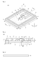
Fig. 1 is a perspective view of a light emitting device according to a first embodiment. -
Fig. 2 is a side sectional view taken along line A-A ofFig. 1 . -
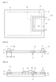
Figs. 3 to 10 are views illustrating a process of manufacturing the light emitting device ofFig. 1 . -
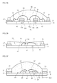
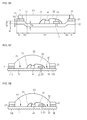
Figs. 11 and 12 are side sectional views of a light emitting device according to second and third embodiments. -
Figs. 13 and 14 are perspective and side sectional views of a light emitting device according to a fourth embodiment. -
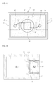
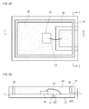
Figs. 15 and 16 are plan and side sectional views of a light emitting device according to a fifth embodiment. -
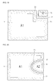
Fig. 17 is a view illustrating a modified example of the light emitting device ofFig. 15 . -
Figs. 18 to 27 are views illustrating modified examples of a metal layer and an insulation film according to an embodiment. -
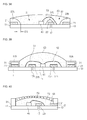
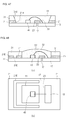
Figs. 28 to 51 are views illustrating modified examples of a light emitting device according to another embodiment. -
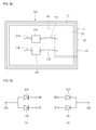
Figs. 52 and 53 are a side sectional view and a circuit diagram illustrating another example of a light emitting device according to an embodiment. -
Figs. 54 and 55 are a side sectional view and a circuit diagram illustrating another example of a light emitting device according to an embodiment. -
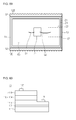
Fig. 56 is a side sectional view illustrating a modified example of a metal layer of a light emitting device according to an embodiment. -
Figs. 57 to 59 are views illustrating modified examples of a metal layer of a light emitting device according to an embodiment. -
Figs. 60 and61 are views illustrating an example of a light emitting chip according to an embodiment. -
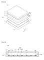
Fig. 62 is a perspective view illustrating an example of a display device according to an embodiment. -
Fig. 63 is a perspective view illustrating another example of the display device according to an embodiment. -
Fig. 64 is a view of a lighting unit according to an embodiment. - In the description of embodiments, it will be understood that when a layer (or film), region, pattern or structure is referred to as being 'on' or 'under' another layer (or film), region, pad or pattern, the terminology of 'on' and 'under' includes both the meanings of 'directly' and 'indirectly'. Further, the reference about 'on' and 'under' each layer will be made on the basis of drawings.
- In the drawings, the thickness or size of each layer is exaggerated, omitted, or schematically illustrated for convenience in description and clarity. In the drawings, the thickness or size of each layer is exaggerated, omitted, or schematically illustrated for convenience in description and clarity.
- Hereinafter, embodiments will be described with reference to the accompanying drawings.
-
Fig. 1 is a perspective view of a light emitting device according to a first embodiment.Fig. 2 is a side-sectional view taken along line A-A ofFIG. 1 . - Referring to
Figs. 1 and 2 , alight emitting device 100 includes a plurality ofmetal layers metal layers light emitting chip 41 on afirst metal layer 11 of the plurality ofmetal layers guide member 31 on theinsulation films 20, and aresin layer 61 covering thelight emitting chip 41 on themetal layers - The
metal layers metal layers metal layers metal layers - Lower surfaces S3 of the plurality of
metal layers metal layers metal layers - The plurality of
metal layers metal layers metal layers metal layers - When the
metal layers - Each of the metal layers 11 and 13 may have a thickness of about 15 µm to about 300 µm, and preferably, about 15 µm to about 50 µm. Also, the metal layers 11 and 13 may serve as a support frame for supporting the entire light emitting device and a heat-dissipating member for conducting heat generated from the
light emitting chip 41. In outer areas of the metal layers 11 and 13, a length Y1 of a first direction Y and a length X1 of a second direction X perpendicular to the first direction Y may vary according to a size of thelight emitting device 100. - The
light emitting device 100 may not include a separate body, e.g., a resin-based body formed of polyphthalamide (PPA). Thus, injection and molding processes for coupling the metal layers 11 and 13 to the body may be omitted. A portion of each of the metal layers 11 and 13 may have a flexibly curved shape or be bent at a predetermined angle, but is not limited thereto. - Hereinafter, for description of the first embodiment, the metal layers 11 and 13 including a
first metal layer 11 and asecond metal layer 13 will be described as an example. Lower surfaces S3 of thefirst metal layer 11 and thesecond metal layer 13 may be flush with each other. Also, the first and second metal layers 11 and 13 may be bonded to a printed circuit board (PCB) or a heatsink plate using soldering. - A
separation part 17 may be disposed between thefirst metal layer 11 and thesecond metal layer 18. Theseparation part 17 may physically space thefirst metal layer 11 from thesecond metal layer 13. Theseparation part 17 may have one of a straight line shape, a curved line shape, and a bent line shape. The line shape may have a width or shape varying according to shapes or sizes of the first and second metal layers 11 and 13. Theseparation part 17 divides one metal frame into the first and second metal layers 11 and 13. Also, each of the first and second metal layers 11 and 13 may have a shape or size varying according to a width and position of theseparation part 17. - The first and second metal layers 11 and 13 may be spaced an interval G1 of about 10 µm from each other. The interval G1 may be a width of the
separation part 17. Also, theseparation part 17 may prevent the twometal layers separation part 17 may be empty or filled with a material, but is not limited thereto. - The first or
second metal layer - An oxidation prevention layer may be disposed on surfaces of the first and second metal layers 11 and 13 and is formed of Au layer. The oxidation prevention layer may prevent the surfaces of the first and second metal layers 11 and 13 from being deformed.
-
Insulation films insulation films first metal layer 11 or/and thesecond metal layer 13. - The
insulation films insulation films metal layers insulation films - Each of the
insulation films insulation films - Adhesion layers may be disposed between the
insulation films insulation films insulation films - Each of the
insulation films insulation films light emitting device 100. - Also, each of the
insulation films insulation films insulation films insulation films insulation films light emitting chip 41 to emit light having a different wavelength. - Also, each of the
insulation films - A portion of a top, lower, or side surface of each of the
insulation films - Each of the
insulation films insulation films - The
insulation films first insulation film 21 disposed on a periphery portion of top surfaces of the twometal layers second insulation film 23 disposed on a top surface of a boundary area of the first and second metal layers 11 and 13. Thesecond insulation film 23 may be a portion of thefirst insulation film 21. Also, thesecond insulation film 23 may be integrally connected to thefirst insulation film 21. The first andsecond insulation films - The
first insulation film 21 may have a constant width W1. Alternatively, thefirst insulation film 21 may have widths different from each other. Thefirst insulation film 21 may have a width W1 of at least several ten µm or more. Thesecond insulation film 23 may have a constant width W2. Alternatively, thesecond insulation film 23 may have widths different from each other. Thesecond insulation film 23 may have a width W2 wider than the interval G1 between the metal layers 11 and 13. For example, thesecond insulation film 23 may have a width of about 20 µm or more. The width W1 of thefirst insulation film 21 may be equal to or different from the W2 of thesecond insulation film 23. Thesecond insulation film 23 may have a width of at least 20 µm or more to support the twometal layers - The
second insulation film 23 may correspond between thefirst metal layer 11 and thesecond metal layer 13. Also, thesecond insulation film 23 may be disposed on the top surfaces of the first and second metal layers 11 and 13 with a width wider than the interval between the metal layers 11 and 13. - Outer surfaces of the
insulation films insulation films - Also, the
first insulation film 21 may be continuously or discontinuously disposed. The continuous film may have a structure in which one film is provided, and the discontinuous film may have a structure in which plurality of films are provided. - The
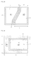
insulation films first metal layer 11 or/and thesecond metal layer 13 is(are) exposed through the inside of each of theinsulation films - The opened areas A1 and A2 may include a first opened area A1 through which a portion of the top surface of the
first metal layer 11 is exposed and a second opened area A2 through which a portion of the top surface of thesecond metal layer 13 is exposed. The first opened area A1 may have a size and shape equal to or different from those of the second opened area A2. In the current embodiment, although the two opened areas A1 and A2 are provided when the twometal layers more metal layers insulation films - One of the plurality of opened areas A1 and A2, e.g., the second opened area S2 may have a minimum width of about 60 µm. When the second opened area A2 has a narrow width, the bonding of a
second wire 52 may be interrupted. Thus, the second opened area A2 may have a width of at least 60 µm. The first opened area A1 may have a width enough to mount thelight emitting chip 41. Also, the first opened area A1 may have a width wider than that of the second opened area A2. Here, although the first opened area A1 is described as an area on which thelight emitting chip 41 is mounted and the second opened area A2 is described as an area to which asecond wire 52 is bonded, the present disclosure is not limited thereto. For example, the first opened area A1 may be an area to which asecond wire 52 is bonded and the second opened area A2 may be an area on which thelight emitting chip 41 is mounted. - The
guide member 31 may be disposed on thefirst insulation film 21. Theguide member 31 may be formed of a resin material, a non-metallic material, or a metallic material. Theguide member 31 may be defined as a reflective member or/and a dam member for preventing the resin material from overflowing. - The
guide member 31 may be formed of a resin material such as solder resist or a conductive material such as solder paste. The solder resist may have a white color. Thus, incident light may be effectively reflected by the white color. Also, theguide member 31 may be formed of a metallic material, e.g., Ag, Al, Cu, Au, Ag-alloy, Al-alloy, Cu-Alloy, or Au-alloy. The metal may be provided as a single or multi layer. Also, theguide member 31 may include a reflective layer on a metal seed layer, e.g., at least one of Ag, Al, and Ni layers through a plating process. - Also, the
guide member 31 may be formed of non-metallic material. The non-metallic material may include a resin having a white color, e.g., a resin material (e.g., PPA) having at least one of solder resist, titanium dioxide (TiO2) and glass fiber or a polymer material (e.g., silicon-based or epoxy-based material). Alternatively, the non-metallic material may include a material equal to that of the insulation film. - The
guide member 31 may be formed of a metal or non-metallic material having a reflection characteristic of about 50% or more, and preferably, a reflection characteristic of about 90% or more. - The
guide member 31 may have a thickness T2 of about 15 µm to about 500 µm. Also, theguide member 31 may have a thickness equal to or different from that of each of theinsulation films guide member 31 may have a thickness thicker than that of each of theinsulation films guide member 31 may have a thicker thickness in consideration of distribution of an orientation angle of light. Also, a top surface of theguide member 31 may be higher than that of thelight emitting chip 41 to reflect light. - The
guide member 31 may be disposed on thefirst insulation film 21 to correspond to a surrounding of the light emitting chip 14. Theguide member 31 may be a frame, ring, or loop shape when viewed from a top side thereof. Theguide member 31 may have a circular or polygonal shape when viewed from a top side thereof Also, theguide member 31 may prevent theresin layer 61 from overflowing. - The
guide member 31 may have a width equal to or different from that of thefirst insulation film 21. When theguide member 31 has a width equal to that of thefirst insulation film 21, the surface reflection efficiency may be improved. When theguide member 31 has a width less than that of thefirst insulation film 21, theguide member 31 may be stably disposed on thefirst insulation film 21. Since theguide member 31 is disposed along thefirst insulation film 21, theguide member 31 may have the opened area. - When the
guide member 31 has conductivity, theguide member 31 may be disposed on the top surface of thefirst insulation film 21. Also, a portion of theguide member 31 may contact one of the plurality ofmetal layers guide member 31 is formed of an insulation material, theguide member 31 may contact top surfaces of the metal layers 11 and 13. - The
light emitting chip 41 may be disposed on thefirst metal layer 11 and electrically connected to the first and second metal layers 11 and 13. - The
light emitting chip 41 may be a light emitting diode having a wavelength band of visible light and emitting red, green, blue, or white light or a light emitting diode having a wavelength band of ultraviolet light, but is not limited thereto. - The
light emitting chip 41 may be realized as a lateral type chip in which two electrodes are disposed in parallel to each other or a vertical type chip in which two electrodes are disposed on sides opposite to each other. The lateral type chip may be connected to at least twowires - The
light emitting chip 41 may adhere to thefirst metal layer 11 using a conductive or insulation adhesive. Here, when an electrode is disposed on a lower portion of thelight emitting chip 41, the conductive adhesive may be used. Also, when an insulation substrate is disposed on the lower portion, the conductive adhesive or the insulation adhesive may be used. - The
light emitting chip 41 may be connected to thefirst metal layer 11 using afirst wire 51 and thesecond metal layer 13 using asecond wire 52. Also, thelight emitting chip 41 may be electrically connected to the first and second metal layers 11 and 13 in a flip chip type. - Although the
light emitting chip 41 is disposed on thefirst metal layer 11, thelight emitting chip 41 may be disposed on thefirst metal layer 11 and/or thesecond metal layer 13, but is not limited thereto. - The
light emitting chip 41 may be connected to thefirst metal layer 11 using thefirst wire 51 and thesecond metal layer 13 using thesecond wire 52. Here, thelight emitting chip 41 may have a thickness of about 80 µm or more. The highest point of one of thewires light emitting chip 41. - A phosphor layer may be coated on the surface of the
light emitting chip 41. The phosphor layer may be disposed on the top surface of thelight emitting chip 41. - Also, a protective device such as a Zener diode or transient voltage suppressor (TVS) diode for protecting the
light emitting chip 41 may be disposed on or under at least one of the first and second metal layers 11 and 13. The protective device may be electrically connected to thelight emitting device 41. The protective device may be connected to the first and second metal layers 11 and 13 and connected to thelight emitting chip 41 in parallel. Thus, the protective device may protect thelight emitting chip 41 against an abnormal voltage applied into thelight emitting chip 41. The protective device may be omitted. - The
resin layer 61 may be disposed on the first and second metal layers 11 and 13. A portion of theresin layer 61 may be disposed on the top surface of thefirst insulation film 21. Theresin layer 61 is disposed on an opened area inside theguide member 31. The opened area of theguide member 31 may be greater than the first and second opened areas A1 and A2. Theresin layer 61 may cover the inner area of theguide member 31, e.g., the first opened area A1 and the second opened area A2. Theresin layer 61 may be physically separated from the first opened area A1 and the second opened area A2. - The
resin layer 61 may be formed of a transparent resin-based material, e.g., silicon or epoxy resin. - The
resin layer 61 may have a thickness T3 of about 80 µm to about 500 µm. Theresin layer 61 may be provided as a single or multi layer. When theresin layer 61 has the multi-layered structure, the lowermost layer may have a thickness less than that of about 80 µm. - When the
resin layer 61 has the multi-layered structure, theresin layer 61 may be stacked with the same material as or materials different from each other. Alternatively, the multi layers may be stacked in an order of from a layer having a low hardness to a layer having a high hardness or from a layer having a high reflective index to a layer having a low reflective index. - A portion of a top surface of the
resin layer 61 may be lower than that of theguide member 31 or higher than that of each of theinsulation films resin layer 61 may be disposed at a height enough to cover thewires - The
resin layer 61 may include a phosphor. The phosphor may include at least one of phosphors having a wavelength band of visible light such as yellow, green, or red light. Theresin layer 61 may be classified into a transparent resin layer and a phosphor layer. The transparent resin layer and the phosphor layer may be stacked to form theresin layer 61. A phosphor film, e.g., a photo luminescent film (PLF) may be disposed above/under theresin layer 61, but is not limited thereto. - A lens may be disposed on the
resin layer 61. The lens may have a convex lens shape, a concave lens shape, or a convex-concave lens shape. Also, the lens may contact or be spaced from a top surface of theresin layer 61, but is not limited thereto. -
Figs. 3 to 10 are views illustrating a process of manufacturing the light emitting device ofFig. 1 . - Referring to
Figs. 3 and4 , ametal layer 10 may have a size enough to manufacture one light emitting device as shown inFig. 1 . Alternatively, themetal layer 10 has a size having a bar shape and enough to manufacture a plurality of light emitting devices arrayed in a first direction (horizontal or vertical direction) or a size having a matrix form and enough to manufacture a plurality of light emitting devices arrayed in horizontal and vertical directions. The metal layer for manufacturing the plurality of light emitting devices may be cut into a unit of an individual light emitting device or two or more light emitting devices. Hereinafter, for description of the current embodiment, a metal layer for manufacturing one light emitting device will be described as an example. - For example, the
metal layer 10 may be realized as a metal plate such as a lead frame. Themetal layer 10 may be formed of Fe, Cu, an alloy containing Fe such as Fe-Ni, Al, an alloy containing Al, or an alloy containing Cu such as Cu-Ni and Cu-Mg-Sn. Themetal layer 10 may be formed as a single or multi layer. Also, a reflective layer formed of Al, Ag, Au, or solder resist or a bonding layer may be formed on top and/or lower surfaces of themetal layer 10. The plating process or costing process of the metal layer may be performed before or afterinsulation films - The
metal layer 10 may have a thickness of about 15 µm to about 300 µm. Thus, themetal layer 10 may serve as a support frame for supporting the light emitting device. - Since the
metal layer 10 is not provided as a separate body, e.g., is not injection-molded with a resin-based body formed of polyphthalamide (PPA), a portion of themetal layer 10 may have a flexibly curved shape or be bent at a predetermined angle. -
Fig. 4 is a sectional view of an insulation film on the metal layer, andFig. 5 is a plan view ofFig. 4 . - Referring to
Figs. 4 and 5 , insulation films 20 (21 and 23) is formed on themetal layer 10. Each of the insulation films 20 (21 and 23) may have a thickness T1 of about 30 µm to about 500 µm in a thickness direction of themetal layer 10. Also, each of the insulation films 20 (21 and 23) may be a thickness thicker than that of themetal layer 10. Here, although the insulation films 20 (21 and 23) are attached to a top surface of the metal layer, themetal layer 10 may be attached to top surfaces of the insulation films 20 (21 and 23). The processes may be changed in order. - The insulation films 20 (21 and 23) may be attached to the
metal layer 10 after an adhesion layer is coated on themetal layer 10. In the adhesion process of theinsulation films metal layer 10, and then, a lamination process is performed at a predetermined temperature to attach theinsulation films metal layer 10. - Each of the
insulation films insulation film insulation films - Each of the
insulation films - When each of the
insulation films insulation films insulation films insulation films - Each of the
insulation films - The
insulation films metal layer 10 after a plurality of opened areas A1 and A2 are formed. The opened areas A1 and A2 may be holes or opened areas formed in a single film. Also, the opened areas A1 and A2 may be areas in which a top surface of themetal layer 10 is exposed through the inside of each of each of theinsulation films insulation films first insulation film 21 formed around the first opened area A1 or themetal layer 10 and asecond insulation film 23 formed around the second opened area A2. Thesecond insulation film 23 may be a portion of thefirst insulation film 21. Also, thesecond insulation film 23 may be integrally formed with thefirst insulation film 21. The first andsecond insulation films - The
first insulation film 21 may have a constant width W1. Alternatively, thefirst insulation film 21 may have widths different from each other. Thefirst insulation film 21 may have a width W1 of several ten µm or more. Thesecond insulation film 23 may have a constant width W2. Alternatively, thefirst insulation film 23 may have widths different from each other. Thesecond insulation film 23 may have a width W2 greater than an interval G1 between the metal layers 11 and 13. For example, thesecond insulation film 23 may have a width of about 20 µm or more. The width W1 of thefirst insulation film 21 may be equal to or different from the W2 of thesecond insulation film 23. - One of the plurality of opened areas A1 and A2, e.g., the second opened area A2 may have a minimum width of about 60 µm. The second opened area A2 may have a width at which a bonding process of a wire is not interrupted. The first opened area A1 may have a width enough to mount a light emitting chip. Also, the first opened area A1 may have a width wider than that of the second opened area A2. Here, although the first opened area A1 is described as an area on which the light emitting chip is mounted and the second opened area A2 is described as an area to which the wire is bonded, the present disclosure is not limited thereto. For example, the first opened area A1 may be an area to which the wire is bonded and the second opened area A2 may be an area on which the light emitting chip is mounted.
- A punching process, a cutting process, or an etching process may be performed on a single insulation film to form the first opened area A1 and the second opened area A2. The first and second opened areas A1 and A2 may be changed in width or shape. The opened areas A1 and A2 may be formed before or after the insulation films 20 (21 and 23) are attached to the
metal layer 10. - A top surface of the
metal layer 10 may be exposed through the first and second opened areas A1 and A2 of theinsulation films - For example, each of the
insulation films insulation films - Each of the
insulation films insulation films - Referring to
Figs. 6 and7 , themetal layer 10 ofFig. 4 may be divided into a plurality ofmetal layers metal layers metal layers - Here, in a process for forming a circuit of the metal layer, for example, after a surface of the lead frame is activated, a photoresist may be coated, an exposure process may be performed, and a developing process may be performed. When the developing process is completed, an etching process may be performed to form a required circuit and exfoliate the photoresist. Thereafter, an Ag plating process may be performed on a surface of the metal layer to treat the surface of the metal layer to a bondable surface.
- The
first metal layer 11 may have a width equal to or different from that of thesecond metal layer 13. For example, thefirst metal layer 11 may have a size greater or less than that of thesecond metal layer 13. Alternatively, the first and second metal layers 11 and 13 may have the same area as each other or shapes symmetric to each other. - A
predetermined separation part 17 may be disposed between the first and second metal layers 11 and 13 to space thefirst metal layer 11 from thesecond metal layer 13. The first and second metal layers 11 and 13 may be spaced an interval G1 of about 10 µm or more from each other. The interval G1 may be less than a width W1 of thesecond insulation film 23. - The
second insulation film 23 may maintain the interval G1 between the first and second metal layers 11 and 13, and thefirst insulation film 21 may support the metal layers 11 and 13. - Here, the
second metal layer 13 may extend inward through one side surface of thefirst metal layer 11. Thesecond meal layer 13 may have left and right lengths D1 and D2 which vary according to the second opened area A2 and theinsulation films - Referring to
Figs. 6 and8 , aguide member 31 is formed on top surfaces of theinsulation films guide member 31. In the printing process, a masking process may be performed on an area except an area to be printed and a screen printing process may be performed to form theguide member 31. In the coating process, a reflective material may be coated to form theguide member 31. In the film adhesion process, a film such as a reflective sheet may adhere to form theguide member 31. Here, materials of theguide member 31 and theinsulation films - The
guide member 31 may be formed in the printing manner using solder resist or solder paste. The solder resist may have a white color to effectively reflect incident light. Also, theguide member 31 may be formed of a high-reflective material, e.g., Ag, Al, Cu, Au, Ag-alloy, Al-alloy, Cu-Alloy, or Au-alloy. The reflective material may be provided as a single or multi layer. Also, a plating process may be performed on a metal seed layer, e.g., on a material such as Ag, Al, or Ni to form theguide member 31. - Also, the
guide member 31 may be formed of a non-metallic material. The non-metallic material may include a white resin, for example, a resin (e.g., PPA) in which TiO2 and glass fiber are mixed. When theguide member 31 has insulating and reflective characteristics, a separate insulation film may be unnecessary, but is not limited thereto. - The
guide member 31 may be formed of a metal or non-metal material having a reflection characteristic of about 50% or more, and preferably, a reflection characteristic of about 90% or more. - The
guide member 31 may have a thickness T2 of about 15 µm to about 500 µm. Also, theguide member 31 may have a thickness equal to or different from that of each of theinsulation films guide member 31 may have a thickness T2 and an arrangement structure which vary in consideration of distribution of an orientation angle of light. - The
guide member 31 may be formed on thefirst insulation film 21 to cover a surrounding of the light emitting chip 14. Theguide member 31 may be a frame, ring, or loop shape when viewed from a top side. Theguide member 31 may be continuously or discontinuously formed on the top surface of thefirst insulation film 21 - The
guide member 31 may have a width W3 equal to or different from that of thefirst insulation film 21. When theguide member 31 has a width equal to that of thefirst insulation film 21, the surface reflection efficiency may be improved. When theguide member 31 has a width different from that of thefirst insulation film 21, theguide member 31 may be stably disposed on thefirst insulation film 21. - When the
guide member 31 has conductivity, theguide member 31 may be disposed on the top surface of thefirst insulation film 21. Also, a portion of theguide member 31 may contact one of the twolead frames guide member 31 is formed of an insulation material, theguide member 31 may extend from the top surface of thefirst insulation film 21 to the top surfaces of the metal layers 11 and 13. - Referring to
Figs. 8 and 9 , thelight emitting chip 41 may be disposed on thefirst metal layer 11 and electrically connected to the first and second metal layers 11 and 13. - The
light emitting chip 41 may be a light emitting diode having a wavelength band of visible light and emitting red, green, blue, or white light or a light emitting diode having a wavelength band of ultra violet ray, but is not limited thereto. - The
light emitting chip 41 may be realized as a lateral type chip in which two electrodes are disposed in parallel to each other or a vertical type chip in which two electrodes are disposed on sides opposite to each other. The lateral type chip may be connected to at least twowires - The
light emitting chip 41 may adhere to thefirst metal layer 11 using a conductive or insulation adhesive. Here, when an electrode is disposed on a lower portion of thelight emitting chip 41, the conductive adhesive may be used. Also, when an insulation substrate is disposed on the lower portion, the conductive adhesive or the insulation adhesive may be used. - The
light emitting chip 41 may be connected to thefirst metal layer 11 using afirst wire 51 and thesecond metal layer 13 using asecond wire 51. Also, thelight emitting chip 41 may be electrically connected to the first and second metal layers 11 and 13 in a flip chip type. - Although the
light emitting chip 41 is disposed on thefirst metal layer 11, thelight emitting chip 41 may be disposed on thefirst metal layer 11 and/or thesecond metal layer 13, but is not limited thereto. - The
light emitting chip 41 may be connected to thefirst metal layer 11 using thefirst wire 51 and thesecond metal layer 13 using thesecond wire 52. Here, thelight emitting chip 41 may have a thickness of about 80 µm or more. The highest point of one of thewires light emitting chip 41. - Referring to
Figs. 9 and10 , theresin layer 61 may be formed of a transparent resin-based material, e.g., silicon or epoxy resin. - The
resin layer 61 may have a thickness T3 of about 80 µm to about 500 µm. Theresin layer 61 may be provided as a single or multi layer. When theresin layer 61 has the multi-layered structure, the lowermost layer may have a thickness less than that of about 80 µm. - When the
resin layer 61 has the multi-layered structure, theresin layer 61 may be stacked with the same material as or materials different from each other. Alternatively, the multi layers may be stacked in an order of from a material having a low hardness to a material having a high hardness or from a material having a high reflective index to a material having a low reflective index. - A portion of a top surface of the
resin layer 61 may be lower than that of theguide member 31 or higher than that of each of theinsulation films resin layer 61 may be disposed at a height enough to cover thewires - The
resin layer 61 may include a phosphor. The phosphor may include at least one of phosphors having a wavelength band of visible light such as yellow, green, or red light. Theresin layer 61 may be classified into a transparent resin layer and a phosphor layer. The transparent resin layer and the phosphor layer may be stacked to form theresin layer 61. A phosphor film, e.g., a photo luminescent film (PLF) may be disposed above/under theresin layer 61, but is not limited thereto. - The
resin layer 61 may cover the inner area of theguide member 31, e.g., the first opened area A1 and the second opened area A2. Theresin layer 61 may be physically separated from the first opened area A1 and the second opened area A2. - A lens may be disposed on the
resin layer 61. The lens may have a convex lens shape, a concave lens shape, or a convex-concave lens shape, but is not limited thereto. Also, the lens may contact or be spaced from a top surface of theresin layer 61, but is not limited thereto. -
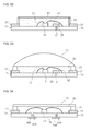
Fig. 11 is a side sectional view of a light emitting device according to a second embodiment. - Referring to
Fig. 11 , alight emitting chip 41 may be bonded on afirst metal layer 11. Also, thelight emitting chip 41 may be electrically connected to thefirst metal layer 11 and connected to asecond metal layer 13 through awire 52. - An
insulation film 24 may be attached to a lower side between thefirst metal layer 11 and thesecond metal layer 13. Theinsulation film 24 may maintain a predetermined interval between thefirst metal layer 11 and the second metal layer and support a portion between thefirst metal layer 11 and thesecond metal layer 13. - A
resin layer 61 is disposed on thefirst metal layer 11 and thesecond metal layer 13. Theresin layer 61 may be injection-molded in a predetermined shape through a transfer molding method. According to the transfer molding method, a liquid resin is filled into a frame having a predetermined shape and then cured so that theresin layer 61 having a desired shape may be formed. Theresin layer 61 may have a cylindrical shape, a polygonal column shape, or uneven surface shape, but is not limited thereto. - A
portion 61A of theresin layer 61 may be disposed between thefirst metal layer 11 and thesecond metal layer 13 and may contact a top surface of theinsulation film 24. - An outer surface of the
resin layer 61 may be spaced a predetermined interval T3 inward from an outer part of thefirst metal layer 11 or thesecond metal layer 13. Accordingly, the outer top surfaces of thefirst metal layer 11 and thesecond metal layer 13 may be exposed. The interval T3 may be about 1 µm or more. - Also, a reflective layer may be further disposed on a portion of a top surface or a side surface of the
resin layer 61, but is not limited thereto. -
Fig. 12 is a side sectional view of a light emitting device including a plurality of light emitting chips according to a third embodiment. - Referring to
Fig. 12 , a light emitting device includes three ormore metal layers light emitting chips light emitting chips - The metal layers 11A, 11B, and 11C are arrayed on the same plane. A
first insulation film 21 is disposed around the metal layers 11A, 11B, and 11C.Second insulation films metal layers metal layers third insulation layer 22 may be disposed at a center side of thesecond metal layer 11B and divided into two areas. - The first to
third insulation films - A first
light emitting chip 41A and a secondlight emitting chip 41B are spaced from and disposed on thesecond metal layer 11B. Athird insulation film 22 is disposed between the firstlight emitting chip 41A and the secondlight emitting chip 41B. - A
guide member 31 is disposed on thefirst insulation film 21 and thethird insulation film 22. Theguide member 31 is disposed at a position higher than a top surface of thelight emitting chip 41 to reflect light emitted from thelight emitting chips - Resin layers 62 and 63 are disposed on the first and second
light emitting chips guide member 31, but are not limited thereto. - The
second metal layer 11B may serve as common electrodes of the firstlight emitting chip 41A and the secondlight emitting chip 41B. Thefirst metal layer 11A may serve as an electrode for controlling the firstlight emitting chip 41A, and thethird metal layer 11C may serve as an electrode for controlling the secondlight emitting chip 41B. - According to the current embodiment, although it is described that the two
light emitting chips third insulation film 22 is cut, the light emitting device may be manufactured into two light emitting devices. -
Figs. 13 and 14 are perspective and side sectional views of a light emitting device according to a fourth embodiment. - Referring to
Figs. 13 and 14 , aninsulation film 25 adheres to a circumference on a top surface of asecond metal layer 13 to support afirst metal layer 11 and asecond metal layer 13. Theinsulation film 25 covers aseparation part 17 between thefirst metal layer 11 and thesecond metal layer 13 to support a portion between thefirst metal layer 11 and thesecond metal layer 13. - A
guide member 32 is disposed around a top surface of thefirst metal layer 11. A portion of theguide member 32 may be disposed on an outer top surface of theinsulation film 25. Theguide member 32 may be disposed around the top surface of thefirst metal layer 11 and on the outer top surface of theinsulation film 25. Theguide member 32 may be electrically connected on the top surface of thefirst metal layer 11 and electrically separated from the top surface of thesecond metal layer 13 by theinsulation film 25. Theguide member 32 may be disposed around thefirst metal layer 11 and theinsulation film 25 in a loop shape, a frame shape, or a ring shape. Theinsulation film 25 may be disposed around the top surface of thesecond metal layer 13 in a loop shape, a frame shape, or a ring shape. - The
insulation film 25 may prevent theguide member 32 from physically or electrically contacting thesecond metal layer 13 and prevent the first and second metal layers 11 I and 13 from being short-circuited. Theinsulation film 25 and theguide member 32 may support and fix the twometal layers guide member 31 may have a thickness equal to that of theresin layer 61. - According to the current embodiment, the
insulation film 25 may decrease in area and theguide member 32 may increase in area to improve optical reflection efficiency. -
Figs. 15 and 16 are plan and side sectional views of a light emitting device according to a fifth embodiment. - Referring to
Figs. 15 and 16 ,insulation films light emitting chip 41 is mounted on afirst metal layer 11, a second opened area A2 to which asecond wire 52 is bonded on asecond metal layer 12, and a third opened area A3 to which afirst wire 51 is bonded on thefirst metal layer 11. As another example, the third bonding area A3 may not be defined when thelight emitting chip 41 has a vertical type electrode structure. - Each of the first to third opened areas A1, A2, and A3 may have a circular shape or a polygonal shape. Here, the second opened area A2 may be formed with a size which is less by at least four times or less than a lower area of the
light emitting chip 41. Each of the first and third opened areas A1 and A3 may have width or diameter greater than a diameter (e.g., about 20 µm to about 50 µm) of a wire, for example, about 60 µm to about 120 µm. - Since an adhesion area of each of the
insulation films Fig. 1 , thefirst metal layer 11 and thesecond metal layer 13 may be more firmly supported. Aguide member 31 may be disposed around a top surface of each of theinsulation films resin layer 61 may be molded inside theguide member 31. -
Fig. 17 is a plan view illustrating another example ofFig. 15 . - Referring to
Fig. 17 , a light emitting device includes threemetal layers insulation film 21 attached on the metal layers 11, 13, and 15. A plurality of opened areas A1, A2, and A3 are defined on aninsulation film 21. The plurality of opened areas A1, A2, and A3 may open portions of top surfaces ofmetal layers - The
third metal layer 15 is disposed between thefirst metal layer 11 and thesecond metal layer 13. Alight emitting chip 41 is mounted on thethird metal layer 15. Thelight emitting chip 41 is disposed on a first opened area A1 of theinsulation film 21. Also, a second open area A2 and a third open area A3 may be wire bonding areas. - The
light emitting chip 41 is connected to thefirst metal layer 11 on the third open area A3 through afirst wire 51 and is connected to thesecond metal layer 13 on the second open area A2 through asecond wire 52. - The opened areas A1, A2, and A3 of the
insulation film 21 are areas in which thelight emitting chip 41 and thewires insulation film 21 may firmly support a portion between the metal layers 11, 13, and 15 and prevent a stepped portion between the metal layers 11, 13, and 15 from occurring to improve electrical reliability due to solder bonding and also improve thermal transfer efficiency. -
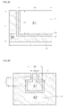
Figs. 18 to 27 are views illustrating modified examples of a metal layer and an insulation film according to an embodiment. - Referring to
Fig. 18 , asecond metal layer 13 may be disposed on at least portion of afirst metal layer 11 and may have a circular shape, a polygonal shape, or a random shape at a side of thefirst metal layer 11. Aseparation part 17 between thefirst metal layer 11 and thesecond metal layer 13 may have a uniform or irregular width. - The
first metal layer 11 and thesecond metal layer 13 may have surfaces mutually corresponding to each other and havingroughness structures 11D and 13D. Theroughness structures 11D and 13D may improve the adhesion efficiency of thesecond insulation film 23. - As shown in
Fig. 19 , thesecond metal layer 13 may be disposed in a predetermined shape, e.g., a circular or polygonal shape, on at least one edge of thefirst metal layer 11. - As shown in
Figs. 20 and21 , thesecond metal layer 13 may be have a hemispherical shape on at least portion of thefirst metal layer 11 or may have a polygonal shape on an edge of thefirst metal layer 11. - As shown in
Fig. 22 , the second andthird metal layers first metal layer 11. The second andthird metal layers first metal layer 11. The second andthird metal layers third metal layers insulation films metal layers insulation films metal layers - As shown in
Fig. 23 , thefirst metal layer 11 and thesecond metal layer 13 are divided by theseparation part 17 at a center side thereof. Also, the first and second metal layers 11 and 13 may have the same area as or symmetrical to each other. A length L1 of a first side of thesecond metal layer 13 may be less than that L2 of a second side opposite to the first side, but is not limited thereto. - Referring to
Fig. 24 , thesecond metal layer 13 may be disposed on a portion of thefirst metal layer 11. Thesecond metal layer 13 may have a first direction width X3 having a size of about 1/2 times than a second direction width X2 of thesecond metal layer 11. - The
second metal layer 13 may have a first direction width Y3 having a size of about 1/2 times than a second direction width Y1 of thefirst metal layer 11. - An
insulation film 21 is disposed on a boundary between the first and second metal layers 11 and 13. Theinsulation film 21 covers an area except the second opened area A2. An outer top surface of thesecond metal layer 13 may be exposed without providing theinsulation film 21. - A light emitting chip may be mounted on the opened area A1 of the
second metal layer 13. The light emitting chip may be electrically connected to the twometal layers - Referring to
Fig. 25 , thesecond metal layer 13 may be disposed on an edge portion of thefirst metal layer 11. A first direction width X4 and a second direction width Y4 of thesecond metal layer 13 may be about 1/2 times or more than the first direction width X1 and the second direction widths X1 and Y1 of thefirst metal layer 11. - Since a guide member is disposed without providing an insulation film on an outer top surface of the
second metal layer 13, an area covered by the guide member may be improved. - Referring to
Fig. 26 , thesecond metal layer 13 may extend up to the inside of thefirst metal layer 11 through one side surface of thefirst metal layer 11 or may be disposed inside thefirst metal layer 11. - A width W5 of an outer part 13-1 of the
second metal layer 13 may be narrower than a width W6 of an inner part 13-2. The light emitting chip may be disposed on the first opened area A1 of thesecond metal layer 13, but is not limited thereto. - Referring to
Fig. 27 , thesecond metal layer 13 may have a diameter as long as a width of thefirst metal layer 11 and have a hemispheric shape. Aninsulation film 21 may be disposed on the boundary between thefirst metal layer 11 and thesecond metal layer 13. A guide member may be disposed around the top surfaces of themetal layer - <Sixth embodiment>
- Referring to
Fig. 28 , afirst insulation film 21 is disposed around top surfaces of afirst metal layer 11 and asecond metal layer 13. Also, asecond insulation film 23 covering a portion between thefirst metal layer 11 and thesecond metal layer 13 is disposed. Thefirst insulation film 21 and thesecond insulation film 23 may be connected to each other. An opened area may be disposed between thefirst insulation film 21 and thesecond insulation film 23. - A
resin layer 63 is disposed on the opened area of thefirst insulation film 21 to cover alight emitting chip 41. A liquid resin-based insulation material may be dispensed and then cured to form theresin layer 63. Here, thefirst insulation film 21 may serve as a dam around theresin layer 63. Theresin layer 63 may have a surface having a convex lens shape. A center part of theresin layer 63 may have a thickness greater than those of thefirst insulation film 21 and thesecond insulation film 23. - A
guide member 31 or a reflective material may be further disposed around theresin layer 63, but is not limited thereto. - <Seventh embodiment>
- Referring to
Fig. 29 , alight emitting chip 45 is die-bonded to afirst metal layer 11 and is connected to asecond metal layer 13 through a wire. Aresin layer 63 is disposed on thefirst metal layer 11 and thesecond metal layer 13. - The
resin layer 63 is disposed on top surfaces of the metal layers 11 and 13. Aninsulation film 21 is disposed around theresin layer 63. Theresin layer 63 may have a convex lens shape. Aguide member 31 or a reflective material may be further disposed around theresin layer 63, but is not limited thereto. - A
spacer 18 is disposed on aseparation part 17 between thefirst metal layer 11 and thesecond metal layer 13. Thespacer 18 is disposed between thefirst metal layer 11 and thesecond metal layer 13 and is formed of an insulation material. Thespacer 18 adheres between thefirst metal layer 11 and thesecond metal layer 13. Thespacer 18 may space thefirst metal layer 11 from thesecond metal layer 13 to prevent the first and second metal layers 11 and 13 from being electrically short-circuited with each other. Thespacer 18 may be formed of at least one of SiO2, SiOx, SiOxNy, Si3N4, Al2O3, and TiO2. - The
resin layer 63 may have a lower surface contacting top sides of thefirst metal layer 11 and thesecond metal layer 13 and the a top surface of thespacer 18. - <Eighth embodiment>
- Referring to
Fig. 30 , aroughness 63A is disposed on a surface of aresin layer 63. Theroughness 63A may have a rough surface by performing an etching or injecting process on the surface of theresin layer 61. Theroughness 63A may change a critical angle of light traveling to the outside of theresin layer 63 to improve light extraction efficiency. - <Ninth embodiment>
- Referring to
Fig. 31 , alight emitting chip 41 may be mounted on afirst metal layer 11 and asecond metal layer 13 in a flip manner. Thelight emitting chip 41 is mounted on thefirst metal layer 11 and thesecond metal layer 13. Thefirst metal layer 11 and thesecond metal layer 13 may have the same width as each other. - A
second insulation film 24 is attached to lower surfaces of thefirst metal layer 11 and thesecond metal layer 13 to insulate the twometal layers metal layers - A
first insulation film 21 may be attached around top surfaces of thefirst metal layer 11 and thesecond metal layer 13 to fix the twometal layers - The
second insulation film 21 may serve as a dam to prevent theresin layer 63 from overflowing. A portion of theresin layer 63 may be filled between the first and second metal layers 11 and 13 to maintain an interval between thesecond insulation film 21 and the metal layers 11 and 13. - The
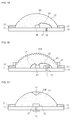
resin layer 63 may have a convex hemispherical shape. Also, aconcave part 63B having a predetermined depth is defined in a center of theresin layer 63. Theconcave part 63B may have a horn shape or a hemispherical shape. Areflective material 72 may be disposed within theconcave part 63B. Thereflective material 72 may include a metal oxide. For example, thereflective material 72 may form at least one layer formed of a material such as TiO2 or/and SiO2 to reflect incident light into a side direction. Theresin layer 63 and thereflective material 72 may have refractive indexes different from each other. For example, thereflective material 72 may have a refractive index greater than that of theresin layer 63. Theresin layer 63 may reflect light of a center direction toward the side direction to uniformly provide orientation angle distribution of the light. - Also, a scattering agent, but the reflective material may be disposed in the
concave part 63B, but is not limited thereto. - <Tenth embodiment>
- Referring to
Fig. 32 , aguide member 33 is formed on a side surface of theresin layer 61. After theresin layer 61 is formed, theguide member 33 may be deposited by performing a sputtering or deposition method on at least two side surfaces of theresin layer 61. Thus, a manufacturing process may be changed due to theguide member 33. A width and thickness of theguide member 33 may be adjusted according to a deposition time. Theguide member 33 may be formed of a reflective material such as A1 or Ag or a light transmitting material having a high refractive index. - <Eleventh embodiment>
- Referring to
Fig. 33 , a light emitting device has a structure in which alens 71 is disposed on aresin layer 61. Alens 71 on theresin layer 61 may have a convex hemispherical shape and may adhere to top surfaces of theresin layer 61 and aguide member 31. Theguide member 31 and thelens 71 may have uneven surfaces, respectively, but are not limited thereto. - <Twelfth Embodiment>
- Referring to
Fig. 34 , a light emitting device includes threemetal layers metal layers third metal layer 15 may be disposed between the first and second metal layers 11 and 13 and used as a heatsink plate. - A
first insulation film 21 is disposed around top surfaces of the first to third metal layers 11, 13, and 15 to serve as a barrier of theresin layer 61 and support the metal layers 11, 13, and 15. Second andthird insulation films third metal layers third metal layers third metal layers third metal layers third insulation films third insulation films - Also, a
portion 61A of theresin layer 61 is filled between the first andthird metal layers third metal layers third insulation films resin layer 61 is cured. The metal layers 11, 13, and 15 may be supported by theresin layer 61 and thefirst insulation film 21 and have a flat lower surface. - A
phosphor layer 73 is disposed above theresin layer 61. Thephosphor layer 73 may be a film including a phosphor or a resin layer to which a phosphor is added. Thephosphor layer 73 may extend from a top surface of theresin layer 61 up to a top side of theguide member 31. Thephosphor layer 73 may absorb a part of light emitted from thelight emitting chip 41 to emit light having a wavelength longer than that of the absorbed light, thereby moving in desired color coordinates in a color coordinate distribution. - <Thirteenth embodiment>
- Referring to
Fig. 35 , a light emitting device has a structure in which a second guide member 35 is further disposed on second andthird insulation films - The second and
third insulation films separation parts adjacent metal layers second guide member 34 is disposed on thesecond insulation films first guide member 31 is disposed on thefirst insulation film 21.Light emitting chips first guide member 31 and thesecond guide member 34. Thefirst guide member 31 and thesecond guide member 34 may be disposed around thelight emitting chips - The first
light emitting chip 41 is disposed on thefirst metal layer 11, the secondlight emitting chip 42 is disposed on thethird metal layer 15, and the thirdlight emitting chip 43 is disposed on thesecond metal layer 13. The firstlight emitting chip 41 is connected to thefirst metal layer 11 and a first electrode of the secondlight emitting chip 42 throughwires light emitting chip 42 is connected to a first electrode of the thirdlight emitting chip 43 through awire 54. A second electrode of the thirdlight emitting chip 43 is connected to thesecond metal layer 13 through awire 52. The secondlight emitting chip 42 is directly connected to other light emitting chips, but is not limited thereto. - The first
light emitting chip 41 may be connected to thefirst metal layer 11 through thewires light emitting chip 41 and the secondlight emitting chip 42 may be correspondingly connected to each other in chip-to-chip through thewires light emitting chip 42 may be connected to the third metal layer through thewires - <Fourteenth embodiment>
- Referring to
Fig. 36 , a light emitting device includes aresin layer 61 having a concave surface S5. For example, theresin layer 61 may have a lens shape in which a side part is high and a center part is low. A gap T6 between the side part and the center part of theresin layer 61 may be about 0.001 mm to about 1 mm. This gap T6 may prevent an optical guide plate from contacting. Thus, abnormal color distribution such as a chromatic blur phenomenon due to the contact of the optical guide plate may be prevented. - <Fifteenth embodiment>
- Referring to
Fig. 37 , afirst guide member 31 may be disposed on afirst insulation film 21 and asecond guide member 36 may be disposed around alight emitting chip 41. Thesecond guide member 36 may be disposed around thelight emitting chip 41. Thesecond guide member 36 may have a thickness thicker or less than that of thelight emitting chip 41. A portion of thesecond guide member 36 is disposed between the light emittingchip 41 and thesecond insulation film 23. Another portion of thesecond guide member 36 may be disposed between the light emittingchip 41 and afirst wire 51. - The
second guide member 36 may have a frame shape, a loop shape, or a ring shape. Thesecond guide member 36 may be disposed within a first opened area A1 of thefirst metal layer 11 to effectively reflect light emitted from thelight emitting chip 41. - The
first guide member 31 may have the same width as thefirst insulation film 21. Thus, after thefirst guide member 31 adheres to thefirst insulation film 21, a process such as punching may be performed. - According to the current embodiment, the
guide members light emitting chip 41 to improve light reflection efficiency and orientation angle distribution. - <Sixteenth embodiment>
- Referring to
Fig. 38 , a light emitting device includes first andthird guide member first insulation film 21. Thefirst guide member 37A may be disposed on top and inner surfaces of thefirst insulation film 21. A portion of thefirst guide member 37A is disposed closer to thelight emitting chip 45 than to thefirst insulation film 21. A lower portion of thefirst guide member 37A may contact the top surface of thefirst metal layer 11. Thethird guide member 37B may be disposed on the top and inner surfaces of thefirst insulation film 21. A portion of thethird guide member 37B is disposed closer to thelight emitting chip 45 than to thefirst insulation film 21. A lower portion of thethird guide member 37B may contact the top surface of thesecond metal layer 13. Thefirst guide member 37A may extend up to top surfaces of the metal layers 11 and 13 by a predetermined interval D3. The interval D3 may be about 0.1 mm or more. - The first and
third guide members third guide members - When each of the first and
third guide members third guide members third guide members first metal layer 11 and thesecond metal layer 13. Accordingly, theguide member 37A contacting the top surface of thefirst metal layer 11 and thethird guide member 37B contacting the top surface of thesecond metal layer 13 may be separated from each other to prevent the first andsecond guide members - Also, the
second guide member 37C may be disposed on top and inner surfaces of thesecond insulation film 23 to contact the top surface of thefirst metal layer 11. Thesecond guide member 37B may be connected to thefirst guide member 37A and may be separated from thethird guide member 37C. Thesecond guide member 37C may be physically spaced from thesecond metal layer 13. - The
first guide member 37A and thesecond guide member 37C may be disposed corresponding to a surrounding of thelight emitting chip 45 to effectively reflect the light emitted from thelight emitting chip 34. Each of thefirst guide member 37A and thesecond guide member 37C may be formed of a resin material, a non-metallic material, or a reflective metal. - Also, the inner surfaces of the
first guide member 37A and thesecond guide member 37C correspond to thelight emitting chip 45 and may have a curved or inclined shape with respect to the top side of thefirst metal layer 11. - The first to
third guide members third guide members - <Seventeenth embodiment>
- Referring to
Fig. 39 , a light emitting device further includesreflective layers guide member 31. - The
reflective layers reflective layers guide member 31 and thefirst insulation film 21. Thereflective layers - According to the above-mentioned embodiments, since the
insulation films insulation film 21, but is not limited thereto. - <Eighteenth embodiment>
- Referring to
Fig. 40 , in a light emitting device, alight emitting chip 45 is bonded to afirst metal layer 11 and asecond metal layer 13 is connected to thelight emitting chip 45 through awire 53. Asecond insulation film 23 may be attached on a top surface between thefirst metal layer 11 and thesecond metal layer 13. - A
guide member 31 is disposed on thefirst metal layer 11 and thefirst insulation film 21 in a continuous or discontinuous shape. For example, theguide member 31 may have a frame shape, a loop shape, and a ring shape. - A
resin layer 63 may be disposed within theguide member 31 and aphosphor layer 73 may be disposed on theresin layer 63. A phosphor of thephosphor layer 73 may be dispersed in an entire area. Also, since the phosphor is spaced from thelight emitting chip 45, discoloration may be prevented. - <Nineteenth embodiment>
- Referring to
Fig. 41 , in a light emitting device, a resin layer is removed and a photo luminescent film 74 is disposed on alight emitting chip 41. The photo luminescent film 74 is disposed spaced from the metal layers 11, 13, and 15 and is supported by theguide member 31. -
Second insulation films - <Twentieth embodiment>
-
Fig. 42 is a side sectional view of a light emitting device, andFig. 43 is a plane view ofFig. 43 . - Referring to
Figs. 42 and 43 , alight emitting chip 41 is mounted on afirst metal layer 11 and asecond metal layer 13 in a flip manner. Aninsulation film 21 is disposed around thefirst metal layer 11 and thesecond metal layer 13. Aspacer 18 formed of an insulation material may be disposed between thefirst metal layer 11 and thesecond metal layer 13. - The
spacer 18 prevents a resin layer from leaking. - The
resin layer 66 may be disposed around thelight emitting chip 41. A portion of theresin layer 66 may extend up to a top surface of theinsulation film 21. - <Twenty first embodiment>
- Referring to
Fig. 44 , in a light emitting device,insulation films first metal layer 11 and asecond metal layer 13. Alight emitting chip 45 is disposed on thefirst metal layer 11 and aresin layer 67 is molded to thelight emitting chip 45. - The
resin layer 67 may have the same side surface as those of thefirst metal layer 11 and thesecond metal layer 13. Theresin layer 67 may have a width corresponding to an interval between both side surfaces of the first and second metal layers 11 and 13. - Here, the
resin layer 67 may have the thickest thickness at acenter part 67A. Also, the thickness T4 of theresin layer 67 may gradually decrease from thecenter part 67A toward the outside. Thecenter part 67A has a convex lens shape. The thickness T4 may be greater or less than a height of thelight emitting chip 45. Thisresin layer 67 may be manufactured using an injection molding frame. Also, since the light emitting device is cut and separated by a size unit of each light emitting device after theresin layer 67 is cured. Therefore, thelight emitting chip 45 may be mounted on or theresin layer 67 may be disposed on the metal layers 11 and 13 during the manufacturing processes. Aseparation part 17 between the metal layers 11 and 13 may be formed through a laser or cutting process after the final resin layer is formed, but is not limited thereto. - <Twenty second embodiment>
- Referring to
Fig. 45 , in a light emitting device, anadhesion layer 29 is disposed betweeninsulation films metal layers adhesion layer 29 may use an insulation adhesive such as silicon or epoxy. Theadhesion layer 29 may have a thickness of about 12 µm or more. - Also, a top surface of the
resin layer 61 may be higher than that of afirst guide member 31 or asecond guide member 31C. - The
second guide member 31C may be disposed on theinsulation film 21 to efficiently reflect light emitted from thelight emitting chip 41. - <Twenty third embodiment>
- Referring to
Fig. 46 , top surfaces of the metal layers 11 and 13 haveuneven structures uneven structures first insulation film 21 and may extend up to opened areas A1 and A2 of each of the metal layers 11 and 13. - The
uneven structures insulation films - <Twenty fourth embodiment>
- Referring to
Fig. 47 , at least one of inner surfaces of an insulation film and aguide member 31 may haveinclined planes inclined planes first insulation film 21 to the inner surface of theguide member 31. Theinclined sides first insulation film 21 and theguide member 31. - Each of the inclined side surfaces 21 d and 31 d may have a tilting angle of about 15° to about 89° with respect to the top surfaces of the metal layers 11 and 13. These inclined side surfaces 21d and 31d may efficiently reflect light in a light emission direction. Also, a reflective material may be coated on the
inclined planes - The
resin layer 61 may have a flat top surface. Theresin layer 61 may have an upper width wider than a lower width thereof due to the inclined side surfaces 21 d and 31 d. - Also, the inner surface of the
second insulation film 23, i.e., a surface corresponding to thelight emitting chip 45 may be inclined, but is not limited thereto. Also, a second guide member may be disposed on thesecond insulation film 23. The second guide member may have an inclined inner surface. - <Twenty fifth embodiment>
-
Fig. 49A is a side sectional view of a light emitting device.Fig. 49B is a plan view of a case in which an insulation film is disposed on a metal layer ofFig. 49A . - Referring to
Fig. 48 , ahole 21E is defined in afirst insulation film 21 on afirst metal layer 11. Thehole 21E exposes a top surface of thefirst metal layer 11. Aguide member 31 may be formed on the first andsecond insulation films portion 31E of theguide member 31 may contact thefirst metal layer 11 through thehole 21E. A portion of theguide member 31 has a protrusion shape. Theguide member 31 has a width less than that of thefirst insulation film 21. - A
portion 31E of theguide member 31 may reflect incident light when thefirst insulation film 21 is formed of a light transmitting material. Also, when theguide member 31 1 and the first metal layer are formed of a metal, theguide member 31 and the first metal layer 11 I may adhere to each other to fix thefirst insulation film 21. - Here, when the
guide member 31 is formed of a non-metallic material or a resin series having non-conductivity, a throughhole 21E of thefirst insulation film 21 may be defined in each of thefirst metal layer 11 and thesecond metal layer 13, except the top surface of the boundary between twometal layers hole 21E may be provided in plurality in thefirst insulation film 21. - <Twenty sixth embodiment>
-
Fig. 49 is a plan view according to an embodiment.Fig. 50 is a sectional view taken along line B-B ofFig. 49 .Fig. 55 is a sectional view taken along line C-C ofFig. 51 . - Referring to
Figs. 49 to 51 , aresin layer 68 is disposed on an entire top surface of first and second metal layers 11 and 13 to mold alight emitting chip 45. Agroove 19 is defined around theresin layer 68. Thegroove 19 may have a ring shape, a frame shape, or a polygonal shape. A top surface of thefirst metal layer 11 may be exposed through thegroove 19 and may be spaced from thesecond metal layer 13. The etching process may include a wet or dry etching process, but is not limited thereto. - A
guide member 38 may be disposed in thegroove 19 and may be formed of a reflective material. Theguide member 38 may be disposed around thelight emitting chip 45 in a circular or polygonal ring shape. Theguide member 38 may contact thefirst metal layer 11 and be spaced a predetermined interval T5 from the second metal layer. Therefore, theguide member 38 may not contact alower portion 68A of theresin layer 68. Here, thelower portion 68A may be a resin layer or an insulating adhesion layer. - When the
guide member 38 is embedded within theresin layer 68, theguide member 38 may contact a top surface of thefirst metal layer 11 and be spaced from thesecond metal layer 13. Also, theguide member 38 may have heights which are different from each other at thefirst metal layer 11 and thesecond metal layer 13. Theguide member 38 may reflect light emitted from thelight emitting chip 45. Since this structure has a structure in which the insulation film is not separately attached, the manufacturing process may be simplified. - A
portion 68C of theresin layer 68 may be filled in aseparation part 17 between thefirst metal layer 11 and thesecond metal layer 13 or an insulation film may be attached to the top or/and lower surface(s) of the metal layers. - The
guide member 38 may have an upper width wider than a lower width. Also, theguide member 38 may have an inner surface inclined at a predetermined angle with respect to the top surfaces of the metal layers 11 and 13. - Features of each embodiment may be selectively applied to other embodiments, are not limited to each embodiment.
- Here, when the
guide member 38 is formed of a non-metallic material or insulation resin series, thegroove 19 of theresin layer 68 may extend to the top surfaces of the first and second metal layers 11 and 13 except a top surface of a boundary between the twometal layers guide member 38 is disposed in thegroove 19. -
Figs. 52 and 53 are a side sectional view and a circuit diagram of a light emitting device according to an embodiment. - Referring to
Fig. 52 , a light emitting device includes three ormore metal layers light emitting chips light emitting chips - The metal layers 12A, 12B, and 12C are arrayed on the same plane. A
first insulation film 21 is disposed around the metal layers 12A, 12B, and 12C.Second insulation films metal layers metal layers - The first
light emitting chip 41A is disposed on thefirst metal layer 12A. The secondlight emitting chip 41B is spaced from thesecond metal layer 12B. - The
second metal layer 12B may serve as common electrodes of the firstlight emitting chip 41A and the secondlight emitting chip 41B. Thefirst metal layer 12A may serve as an electrode for controlling the firstlight emitting chip 41A, and thethird metal layer 12C may serve as an electrode for controlling the secondlight emitting chip 41B. - When the first and second
light emitting chips light emitting chip 41A may be electrically connected to thefirst metal layer 12A and thesecond metal layer 12B through afirst wire 51A and asecond wire 51B, respectively. Also, the secondlight emitting chip 41B may be electrically connected to thesecond metal layer 12B and thethird metal layer 12C through athird wire 51C and afourth wire 51D, respectively. - When the first and second
light emitting chips third wires - A
guide member 31 is disposed on thefirst insulation film 21. Theguide member 31 is disposed at a position higher than those of thelight emitting chips light emitting chips - A
resin layer 61 is disposed on the first and secondlight emitting chips resin layer 61 may be disposed at the same height as or a height less than a top surface of theguide member 31, but are not limited thereto. - Referring to
Fig. 53 , thelight emitting chips first metal layer 12A serves as an anode and thethird metal layer 12B serves as a cathode. Referring toFig. 14 , unlike the circuit illustrated inFig. 14 , the first metal layer may serve as a cathode, and thethird metal layer 12B may serve as an anode. -
Figs. 54 and 55 are a side sectional view and a circuit diagram of a light emitting device according to an embodiment. - Referring to
Fig. 54 , a light emitting device includes three ormore metal layers light emitting chips light emitting chips - The metal layers 12A, 12B, and 12C are arrayed on the same plane. A
first insulation film 21 is disposed around the metal layers 12A, 12B, and 12C. Asecond insulation film 23 is disposed between themetal layers metal layers - The first
light emitting chip 41A and the secondlight emitting chip 41B, which are spaced from each other, are disposed on thefirst metal layer 12A. - The
first metal layer 12A may serve as common electrodes of the firstlight emitting chip 41A and the secondlight emitting chip 41B. Thesecond metal layer 12B may serve as an electrode for controlling the firstlight emitting chip 41A, and thethird metal layer 12C may serve as an electrode for controlling the secondlight emitting chip 41B. - When the first and second
light emitting chips light emitting chip 41A may be electrically connected to thefirst metal layer 12A and thesecond metal layer 12B through afirst wire 51A and athird wire 51C, respectively. Also, the secondlight emitting chip 41B may be electrically connected to thefirst metal layer 12A and thethird metal layer 12C through asecond wire 51B and afourth wire 51D, respectively. - When the first and second
light emitting chips second wires - A
guide member 31 is disposed on thefirst insulation film 21. Theguide member 31 is disposed at a position higher than those of thelight emitting chips light emitting chips - A
resin layer 61 is disposed on the first and secondlight emitting chips resin layer 61 may be disposed at the same height as or a height less than a top surface of theguide member 31, but are not limited thereto. - Referring to
Fig. 55A , thelight emitting chips first metal layer 12A serves as a positive common electrode and the second andthird 12C serve as cathodes. On the other hand, referring tometal layers 12BFig. 55B , thefirst metal layer 12A may serve as a negative common electrode, and the second andthird metal layers -
Fig. 56 is a side sectional view illustrating a modified example of a light emitting device according to a first embodiment. - Referring to
Fig. 56 , alight emitting device 100 includes a plurality ofmetal layers insulation films light emitting chip 41 on at leastmetal layer 11 of the plurality ofmetal layers guide member 31 on theinsulation film 21, and aresin layer 61 covering thelight emitting chip 41 on the metal layers 11 and 13. - Since the metal layers 11 and 13 are not provided as separate bodies, e.g., do not have a structure in which the metal layers 11 and 13 are fixed using a resin-based body formed of polyphthalamide (PPA), a portion of the metal layers 11 and 13 may have a flexibly curved shape, be bent at a predetermined angle, or be partially etched.
- That is, each of the metal layers 11 and 13 include an outer part B1, an inner part B2, and an inclined part B3. A height H2 of a top surface of the outer part B1 of each of the metal layers 11 and 13 may be greater than that H1 of a top surface of the inner part B2 of each of the metal layers 11 and 13.
- Here, the outer part B1 of the
metal layer metal layer - The metal layers 11 and 13 include the inner part B2 and the outer part B1. The outer part B1 may be disposed at a position higher than that of a top surface of the inner part B2. Each of the metal layers 11 and 13 may be bent to form the outer part of each of the metal layers 11 and 13. In the bending process, the inclined part B3 having an inclined plane may be disposed between the inner part B2 and the outer part B1 of the metal layers 11 and 13.
- The inclined part B3 of the plurality of
metal layers - Also, the
light emitting chip 41 and thesecond insulation film 23 may be disposed on the inner part B2 of the metal layers 11 and 13. - Also, the
first insulation film 21 may be disposed on the outer part B1 of the metal layers 11 and 13. Theguide member 31 may be disposed on thefirs insulation film 21. - Although not shown, an inner surface of at least one of the
first insulation film 21 disposed on the outer part B1 and theguide member 31 may be inclined at the inclined angle of the inclined part B3 of the metal layers 11 and 13. -
Figs. 57 to 59 are views illustrating modified examples of a metal layer of a light emitting device according to an embodiment. - Referring to
Fig. 57 , one surface of top, lower, and side surfaces of the metal layers 11 and 13 may have one or moreuneven structures uneven structures first insulation film 21 and may extend up to opened areas A1 and A2 of each of the metal layers 11 and 13. - Also, the
uneven structures light emitting chip 41 is disposed or an area to which thewires light emitting chip 41, and thewires - Each of the
uneven structures - The
uneven structures insulation films - Referring to
Fig. 58 , lower surfaces of the plurality ofmetal layers uneven structures uneven structures - Referring to
Fig. 59 , aheatsink frame 12 may be disposed on one side surface of onemetal layer 11 of the plurality of metal layers. Theheatsink frame 12 may be formed of the same material as themetal layer 11 or a material having conductivity superior than that of themetal layer 11. Theheatsink frame 12 may have a surface having one or moreuneven structures 12E including a concave portion and a convex portion. - Each of the
uneven structures - The thermal efficiency of the metal layers 11 and 13 may be improved through the
uneven structures 12E of theheatsink frame 12. - As another example, the uneven structures may be provided on side surfaces of the plurality of
metal layers - <Light emitting chip>
- A light emitting chip according to an embodiment will be described with reference to
Figs. 60 and61 . - Referring to
Fig. 60 , alight emitting chip 41 may include asubstrate 111, abuffer layer 112, a first conductivetype semiconductor layer 113, anactive layer 114, a second conductivetype semiconductor layer 115, afirst electrode 116, and asecond electrode 117. The first conductivetype semiconductor layer 113, theactive layer 114, and the second conductivetype semiconductor layer 115 may be defined as a light emitting structure. - The
substrate 111 may be formed of Al2O3, GaN, SiC, ZnO, Si, GaP, InP, Ga2O3, a conductive substrate, and GaAs. Thesubstrate 111 may be a growth substrate. A semiconductor having the compositional formula of InxAly Ga1-x-yN (0≤x≤1, 0 ≤y≤1, 0≤x+y≤1) may be grown on the growth substrate. - The
buffer layer 112 may a layer for reducing a lattice constant difference between thesubstrate 111 and the semiconductor and may be formed of a group II to VI compound semiconductor. An undoped Group III-V compound semiconductor layer may be further disposed on thebuffer layer 112, but is not limited thereto. - The first conductive
type semiconductor layer 113 is disposed on thebuffer layer 112, the active layer 124 is disposed on the first conductivetype semiconductor layer 113, and the secondconductive layer 115 is disposed on the active layer 124. - The first conductive
type semiconductor layer 113 may be formed of a group III-V compound semiconductor in which a first conductive type dopant is doped, e.g., one of GaN, AlN, AlGaN, InGaN, InN, InAlGaN, AlInN, AlGaAs, GaP, GaAs, GaAsP, and AlGaInP. When the first conductive type semiconductor layer is an N-type semiconductor layer, the first conductive type dopant may include an N-type dopant such as Si, Ge, Sn, Se, and Te. The second conductivetype semiconductor layer 114 may be formed as a single layer or a multi layer, but is not limited thereto. - The
active layer 114 may have one of a single quantum well structure, a multi quantum well (MQW) structure, a quantum wire structure, and a quantum dot structure. Theactive layer 114 may have a cycle of a well layer and a barrier layer, e.g., an InGaN well layer/GaN barrier layer or a cycle of an InGaN well layer/AlGaN barrier layer using the group III-V compound semiconductor material. - A conductive type clad layer may be disposed above or/and under the
active layer 114. The conductive type clad layer may be formed of an AlGaN-based semiconductor. - A second conductive type is formed on the
active layer 114. The secondconductive semiconductor layer 115 may be formed of a group III-V compound semiconductor in which a second conductive type dopant is doped, e.g., one of GaN, AlN, AlGaN, InGaN, InN, InAlGaN, AlInN, AlGaAs, GaP, GaAs, GaAsP, and AlGaInP. When the second conductive type semiconductor layer is a P-type semiconductor layer, the second conductive type dopant may include a P-type dopant such as Mg and Ze. The second conductivetype semiconductor layer 115 may have a single or multi-layered structure, but is not limited thereto. - A third conductive type semiconductor layer, e.g., an N-type semiconductor layer may be disposed on the second conductive
type semiconductor layer 115. Thus, the light emitting structure 135 may have at least one of an N-P junction structure, a P-N junction structure, an N-P-N junction structure, and a P-N-P junction structure. - A current spreading layer may be disposed on the second conductive
type semiconductor layer 115. The current spreading layer may be formed of one of indium tin oxide (ITO), indium zinc oxide (IZO), indium zinc tin oxide (IZTO), indium aluminum zinc oxide (IAZO), indium gallium zinc oxide (IGZO), indium gallium tin oxide (IGTO), aluminum zinc oxide (AZO), antimony tin oxide (ATO), and gallium zinc oxide (GZO). - A
first electrode 116 may be disposed on the first conductivetype semiconductor layer 113 and asecond electrode 117 may be disposed on the second conductivetype semiconductor layer 115. - The
first electrode 116 and thesecond electrode 117 may be connected to the metal layers ofFig. 1 or5 through a wire. -
Fig. 61 is a view of a vertical type chip structure. - Referring to
Fig. 61 , in alight emitting chip 45, anohmic layer 121 is disposed under alight emitting structure 110, a reflective layer 124 is disposed under theohmic layer 121, a conductive supporting member 125 is disposed under the reflective layer 124, and aprotective layer 123 is disposed around the reflective layer 124 and thelight emitting structure 110. - The
light emitting device 45 may be formed by forming anohmic layer 121, achannel layer 123, a reflective layer 124, and a conductive supporting member 125 on the second conductivetype semiconductor layer 115 and then removing thesubstrate 111 and thebuffer layer 112 without performing an etching process for exposing the first conductivetype semiconductor layer 113 in the structure ofFig. 52 . - The
ohmic layer 121 may ohmic-contact a lower layer of thelight emitting structure 110, for example, the second conductive type semiconductor layer. Theohmic layer 121 may be formed of one of indium tin oxide (ITO), indium zinc oxide (IZO), indium zinc tin oxide (IZTO), indium aluminum zinc oxide (IAZO), indium gallium zinc oxide (IGZO), indium gallium tin oxide (IGTO), aluminum zinc oxide (AZO), antimony tin oxide (ATO), gallium zinc oxide (GZO), Ag, Ni, Al, Rh, Pd, Ir, Ru, Mg, Zn, Pt, Au, Hf and combinations thereof. Also, theohmic layer 121 may be formed as a multi layer using the metal material and a light-transmitting conductive material such as IZO, IZTO, IAZO, IGZO, IGTO, AZO, and ATO. For example, the multi layer may include IZO/Ni, AZO/Ag, IZO/Ag/Ni, and AZO/Ag/Ni. A layer for blocking current corresponding to the electrode 16 may be further disposed within theohmic layer 121. - The
protective layer 123 may be formed of one of indium tin oxide (ITO), indium zinc oxide (IZO), indium zinc tin oxide (IZTO), indium aluminum zinc oxide (IAZO), indium gallium zinc oxide (IGZO), indium gallium tin oxide (IGTO), aluminum zinc oxide (AZO), antimony tin oxide (ATO), gallium zinc oxide (GZO), SiO2, SiOx, SiOxNy, Si3N4, Al2O3, and TiO2. Theprotective layer 123 may be formed through a sputtering method or a deposition method. Theprotective layer 123 may prevent the layers of thelight emitting structure 110 from being electrically short-circuited with each other. - The reflective layer 124 may be formed of one of Ag, Ni, Al, Rh, Pd, Ir, Ru, Mg, Zn, Pt, Au, Hf, and combinations thereof The reflective layer 124 may have a width wider than that of the
light emitting structure 110 to improve light reflection efficiency. - For example, the conductive support member 125 may serve as a base substrate. The conductive support member 125 may be formed of at least one of copper (Cu), gold (Au), nickel (Ni), molybdenum (Mo), copper-tungsten (Cu-W), and carrier wafers (e.g., Si, Ge, GaAs, ZnO, Sic, etc). An adhesion layer may be further disposed between the conductive support member 125 and the reflective layer 124. Thus, the two layers may adhere to each other by the adhesion layer.
- The above-disclosed light emitting chip is just one example and is not limited to the above features. The light emitting chip may be selectively applied to the embodiments of the light emitting device, but is not limited thereto.
- <Lighting system>
- The light emitting device of the above disclosed embodiments has a structure in which the light emitting chip is packaged. Also, a plurality of light emitting devices may be disposed on a board, and thus provided to a lighting system such as a light emitting module or a light unit. One of the light emitting devices according to the above embodiments may be applied to the lighting system.
- The light emitting device according to the embodiment may be applied to the light unit. The light unit may have a structure in which a plurality of light emitting devices are arrayed. The light unit may include the display device illustrated in
Figs. 62 and 63 and the lighting device illustrated inFig. 64 . Furthermore, the light unit may include illumination lamps, traffic lights, vehicle headlights, and signs. -
Fig. 62 is an exploded perspective view illustrating a display device according to an embodiment. - Referring to
Fig. 62 , adisplay unit 1000 may include alight guide plate 1041, alight emitting module 1031 providing light to thelight guide plate 1041, areflective member 1022 under thelight guide plate 1041, anoptical sheet 1051 above thelight guide plate 1041, adisplay panel 1061 above theoptical sheet 1051, and abottom cover 1011 receiving thelight guide plate 1031, thelight emitting module 1031, and thereflective member 1022, but is not limited thereto. - The
bottom cover 1011, thereflective member 1022, thelight guide plate 1041, and theoptical sheet 1051 may be defined as thelight unit 1050. - The
light guide plate 1041 diffuses light to produce planar light. For example, thelight guide plate 1041 may be formed of a transparent material, e.g., one of an acrylic resin-based material such as polymethylmethacrylate (PMMA), a polyethylene terephthalate (PET) resin, a poly carbonate (PC) resin, a cyclic olefin copolymer (COC) resin, and a polyethylene naphthalate (PEN) resin. - The
light emitting module 1031 is disposed to provide light to the at least one lateral surface of thelight guide plate 1041. Thus, thelight emitting module 1031 may be used as a light source of a display device. - At least one light emitting
module 1031 may be disposed on one lateral surface of thelight guide plate 1041 to directly or indirectly provide light. Thelight emitting module 1031 may include aboard 1033 and thelight emitting devices 100 according to the embodiment. Also, thelight emitting devices 100 may be arrayed on theboard 1033 with a predetermined interval. - The
board 1033 may be a printed circuit board (PCB) including a circuit pattern. Theboard 1033 may include a metal core PCB (MCPCB) or a flexible PCB (FPCB) as well as a general PCB, but is not limited thereto. When thelight emitting device 100 are mounted on a lateral surface of thebottom cover 1011 or on a heatsink plate, thesubstrate 1033 may be removed. Here, a portion of the heatsink plate may contact a top surface of thebottom cover 1011. - The plurality of light emitting
devices 100 may be mounted on thesubstrate 1033 to allow a light emission surface through which light is emitted to be spaced a predetermined interval from thelight guide plate 1041, but is not limited thereto. Thelight emitting device 100 may directly or indirectly provide light to a light incident surface that is a side surface of thelight guide plate 1041, but is not limited thereto. - The
reflective member 1022 may be disposed below thelight guide plate 1041. Since thereflective member 1022 reflects light incident onto an lower surface of thelight guide plate 1041 to supply the light upward, brightness of thelight unit 1050 may be improved. For example, thereflective member 1022 may be formed of one of PET, PC, and PVC, but is not limited thereto. Thereflective member 1022 may be the top surface of thebottom cover 1011, but is not limited thereto. - The
bottom cover 1011 may receive thelight guide plate 1041, thelight emitting module 1031, and thereflective member 1022. For this, thebottom cover 1011 may include a receivingpart 1012 having a box shape with an opened upper side, but is not limited thereto. Thebottom cover 1011 may be coupled to a top cover (not shown), but is not limited thereto. - The
bottom cover 1011 may be formed of a metal material or a resin material. Also, thebottom cover 1011 may be manufactured using a press molding process or an extrusion molding process. Thebottom cover 1011 may be formed of a metal or non-metal material having superior heat conductivity, but is not limited thereto. - For example, the
display panel 1061 may be a liquid crystal display (LCD) panel, and include first and second boards formed of a transparent material and a liquid crystal layer between the first and second boards. A polarizing plate may be attached to at least one surface of thedisplay panel 1061. The present disclosure is not limited to the attached structure of the polarizing plate. Thedisplay panel 1061 may display information using light emitted from thelight emitting module 1051. Thedisplay unit 1000 may be applied to various portable terminals, a monitor for a notebook computer, a monitor for a laptop computer, television, etc. - The
optical sheet 1051 is disposed between thedisplay panel 1061 and thelight guide plate 1041 and includes at least one transmission sheet. For example, theoptical sheet 1051 may include at least one of a diffusion sheet, a horizontal or vertical prism sheet, a brightness enhanced sheet, etc. The diffusion sheet diffuses incident light, and the horizontal or/and vertical prism sheet collects the incident light into a display region. In addition, the brightness enhanced sheet reuses lost light to improve the brightness. Also, a protective sheet may be disposed on thedisplay panel 1061, but is not limited thereto. - Here, optical members such as the
light guide plate 1041 and theoptical sheet 1051 may be disposed on an optical path of thelight emitting module 1031, but is not limited thereto. -
Fig. 63 is a view of a display device according to an embodiment. - Referring to
FIG. 63 , adisplay apparatus 1100 includes abottom cover 1152, a board 1120 on which thelight emitting devices 100 described above are arrayed, anoptical member 1154, and adisplay panel 1155. - The substrate 1120 and the
light emitting device 100 may be defined as alight emitting module 1060. Thebottom cover 1152, at least one light emittingmodule 1060, theoptical member 1154 may be defined as the light unit. - The
bottom cover 1152 may include a receivingpart 1153, but is not limited thereto. - Here, the
optical member 1154 may include at least one of a lens, a light guide plate, a diffusion sheet, horizontal and vertical prism sheets, and a bright enhancement sheet. The light guide plate may be formed of a PC material or PMMA material. In this case, the light guide plate may be removed. The diffusion sheet diffuses incident light, and the horizontal and vertical prism sheets collect the incident light into thedisplay panel 1155. The brightness enhanced sheet reuses lost light to improve brightness. - The
optical member 1154 is disposed on thelight emitting module 1060 to produce planar light using the light emitted from thelight emitting module 1060 or diffuse and collect the light emitted from thelight emitting module 1060. -
Fig. 64 is a perspective view of a lighting device according to an embodiment. - Referring to
Fig. 64 , thelighting unit 1500 may include acase 1510, alight emitting module 1530 disposed in thecase 1510, and aconnection terminal 1520 disposed in thecase 1510 to receive an electric power from an external power source. - The
case body 1510 may be formed of a material having good thermal dissipation properties, e.g., a metal material or a resin material. - The
light emitting module 1530 may include aboard 1532 and alight emitting device 100 mounted on theboard 1532. Thelight emitting device 100 may be provided in plurality, and the plurality of light emitting devices 200 may be arrayed in a matrix shape or spaced a predetermined interval from each other. - A circuit pattern may be printed on a dielectric to manufacture the
board 1532. For example, theboard 1532 may include a printed circuit board (PCB), a metal core PCB, a flexible PCB, a ceramic PCB, or a FR-4. - Also, the
board 1532 may be formed of a material which may effectively reflect light or be coated with a color by which light is effectively reflected, e.g., a white color or a silver color. - At least one light emitting
device 100 may be disposed on theboard 1532. Thelight emitting device 100 may include at least one light emitting diode (LED) chip. The LED may include color LEDs, which respectively emit light having a red color, a green color, a blue color, and a white color and an ultraviolet (UV) LED emitting UV rays. - The
light emitting module 1530 may have combinations of several light emittingdevices 100 to obtain desired color and luminance. For example, the white LED, the red LED, and the green LED may be combined with each other to secure a high color rendering index. - The
connection terminal 1520 may be electrically connected to thelight emitting module 1530 to supply a power. Theconnection terminal 1520 may be screwed and coupled to an external power source in a socket type, but is not limited thereto. For example, theconnection terminal 1520 may have a pin shape, and thus, be inserted into the external power source. Alternatively, the connection terminal 1220 may be connected to the external power source by a wire. - According to the embodiments the tape-type or film-type light emitting device may be provided to support the metal layer through the insulation film without using the package body.
- According to the embodiments the manufacturing process of the light emitting device may be improved. Furthermore, the light emitting device may be reduced in thickness. According to the embodiments the light extraction efficiency of the light emitting device may be improved.
- According to the embodiments the reliability of the light emitting device may be improved. Also, the miniaturization and integration of the light emitting device may be improved. According to the embodiments, the thermal efficiency may be improved in the light emitting device and a lighting system having the same.
- Features, structures, and effects described in the above embodiments are incorporated into at least one embodiment of the present disclosure, but are not limited to only one embodiment. Moreover, features, structures, and effects exemplified in one embodiment can easily be combined and modified for another embodiment by those skilled in the art. Therefore, these combinations and modifications should be construed as falling within the scope of the present disclosure.
- Although embodiments have been described with reference to illustrative embodiments thereof, it should be understood that numerous other modifications and embodiments can be devised by those skilled in the art that will fall within the spirit and scope of the principles of this disclosure. More particularly, various variations and modifications are possible in the component parts and/or arrangements of the subject combination arrangement within the scope of the disclosure, the drawings and the appended claims.
Claims (15)
- A light emitting device comprising:a plurality of metal layers spaced from each other;a first insulation film having an opened area in which a portion of top surface area of the plurality of metal layers is opened, the first insulation film being disposed on a periphery portion of top surfaces of the plurality of metal layers;a light emitting chip disposed on at least one of the plurality of metal layers, the light emitting chip being electrically connected to the other metal layer;a resin layer disposed on the plurality of metal layers and the light emitting chip; anda first guide member disposed on the first insulation film.
- The light emitting device according to claim 1, further comprising a second insulation film corresponding to between the plurality of metal layers and having a wider width than an interval between the plurality of metal layers, on at least one of a top surface and a lower surface of the plurality of metal layers.
- The light emitting device according to claim 2, further comprising an adhesive layer between the plurality of metal layers and the first insulation film and the second insulation film.
- The light emitting device according to 3, wherein the first guide member is formed of a metallic material, the first guide member is disposed on at least one of a top surface of the first insulation film and the plurality of metal layers.
- The light emitting device according to claim 2 or 5, further comprising a second guide member on the second insulation film, wherein the first guide member and the second guide member are connected to each other.
- The light emitting device according to any one of claims 2 to 5, wherein the first insulation film and the second insulation film comprise a light-transmitting film or a phosphor film.
- The light emitting device according to claim 6, wherein the first insulation film and the second insulation film comprise at least one selected from the group consisting of a polyimide (PI) film, a polyethylene terephthalate (PET) film, an ethylene vinyl acetate (EVA) film, a polyethylene naphthalate (PEN) film, a tree acetyl cellulose (TAC) film, a polyamide-imide (PAI) film, a polyether-ether-ketone (PEEK) film, a perfluoroalkoxy (PFA) film, a polyphenylene sulfide (PPS), and a resin film.
- The light emitting device according to claim 5, wherein widths of the first and second guide member are narrower than those of the first and second insulation films.
- The light emitting device according to claim 5, wherein the first and second guide members comprise at least one of a resin material, a non- metallic material and a reflective metal.
- The light emitting device according to claim 5, wherein the first and second guide members comprise at least one selected from the group consisting of a solder resist, a solder paste, Ag, Al, Cu, Au, Ag-alloy, Al-alloy, Cu-Alloy, and Au-Alloy.
- The light emitting device according to any one of claims 1 to 4, wherein a thickness of the plurality of metal layers is in a range of about 15 µm to about 300 µm.
- The light emitting device according to any one of claims 1 to 4, wherein the plurality of metal layers comprise a first metal layer, a second metal layer, and a third metal layer between the first metal layer and the second metal layer; and the light emitting chip is disposed on the third metal layer and is electrically connected to the first metal layer and the second metal layer.
- The light emitting device according to any one of claims 1 to 4, further comprising an insulating adhesion material between the plurality of metal layers.
- The light emitting device according to any one of claims 1 to 4, wherein at least one of side surfaces, lower surfaces, and top surfaces of the plurality of metal layers has an uneven structure.
- The light emitting device according to any one of claims 1 to 4, further comprising a third insulation film between the light emitting chip and the first insulation film and a third guide member between the light emitting chip and the first and second insulation films.
Applications Claiming Priority (4)
| Application Number | Priority Date | Filing Date | Title |
|---|---|---|---|
| KR1020100076422 | 2010-08-09 | ||
| KR1020100076425A KR101154656B1 (en) | 2010-08-09 | 2010-08-09 | Light emitting device and lighing system |
| KR1020100076423A KR101114151B1 (en) | 2010-08-09 | 2010-08-09 | Light emitting device and lighting system having same |
| KR1020100076462A KR101172177B1 (en) | 2010-08-09 | 2010-08-09 | Light emitting device and lighing system |
Publications (3)
| Publication Number | Publication Date |
|---|---|
| EP2418700A2 true EP2418700A2 (en) | 2012-02-15 |
| EP2418700A3 EP2418700A3 (en) | 2012-09-19 |
| EP2418700B1 EP2418700B1 (en) | 2017-11-01 |
Family
ID=44381718
Family Applications (1)
| Application Number | Title | Priority Date | Filing Date |
|---|---|---|---|
| EP11176899.0A Not-in-force EP2418700B1 (en) | 2010-08-09 | 2011-08-09 | Light emitting device |
Country Status (5)
| Country | Link |
|---|---|
| US (2) | US8519426B2 (en) |
| EP (1) | EP2418700B1 (en) |
| JP (2) | JP5676395B2 (en) |
| CN (1) | CN102376855B (en) |
| TW (1) | TWI533483B (en) |
Cited By (6)
| Publication number | Priority date | Publication date | Assignee | Title |
|---|---|---|---|---|
| EP2418701A3 (en) * | 2010-08-09 | 2012-09-05 | LG Innotek Co., Ltd. | Light emitting device and lighting system |
| DE102013202551A1 (en) | 2013-02-18 | 2014-08-21 | Heraeus Materials Technologies GmbH & Co. KG | Substrate manufacturing method for LED chip in LED module, involves providing metal layer with cavity, and allowing edge of cavity of substrate to be deformable frontward through deformation that is thicker than metal layer |
| DE102013202542A1 (en) | 2013-02-18 | 2014-09-18 | Heraeus Materials Technology Gmbh & Co. Kg | Substrate for producing an LED and method for its production |
| WO2015040107A1 (en) * | 2013-09-23 | 2015-03-26 | Osram Opto Semiconductors Gmbh | Optoelectronic component and method for producing same |
| CN105591007A (en) * | 2014-10-23 | 2016-05-18 | 展晶科技(深圳)有限公司 | Packaging structure of light-emitting diode |
| DE102020133755A1 (en) | 2020-12-16 | 2022-06-23 | OSRAM Opto Semiconductors Gesellschaft mit beschränkter Haftung | DEVICE WITH STRUCTURED LEAD FRAME AND METHOD OF MAKING DEVICE |
Families Citing this family (53)
| Publication number | Priority date | Publication date | Assignee | Title |
|---|---|---|---|---|
| US8878221B2 (en) | 2011-08-19 | 2014-11-04 | Lg Innotex Co., Ltd. | Light emitting module |
| KR20130096094A (en) * | 2012-02-21 | 2013-08-29 | 엘지이노텍 주식회사 | Light emitting device package, manufactueing method for light emitting device pacakge and lighting system having light emitting device package |
| JP2013206895A (en) * | 2012-03-27 | 2013-10-07 | Shin Etsu Chem Co Ltd | Substrate for optical semiconductor device, manufacturing method of substrate for optical semiconductor device, optical semiconductor device, and manufacturing method of optical semiconductor device |
| KR20130115840A (en) * | 2012-04-13 | 2013-10-22 | 이광희 | Iris identification camera system for mobile device |
| CN103489984B (en) * | 2012-06-13 | 2017-09-12 | 亿光电子工业股份有限公司 | Light emitting diode packaging structure and manufacturing method thereof |
| TWI500185B (en) * | 2012-06-13 | 2015-09-11 | 億光電子工業股份有限公司 | Light-emitting diode package structure and manufacturing method thereof |
| TW201403789A (en) * | 2012-07-06 | 2014-01-16 | 隆達電子股份有限公司 | Light-emitting diode array |
| US8927345B2 (en) * | 2012-07-09 | 2015-01-06 | Freescale Semiconductor, Inc. | Device package with rigid interconnect structure connecting die and substrate and method thereof |
| JP5995579B2 (en) * | 2012-07-24 | 2016-09-21 | シチズンホールディングス株式会社 | Semiconductor light emitting device and manufacturing method thereof |
| US8816507B2 (en) | 2012-07-26 | 2014-08-26 | Taiwan Semiconductor Manufacturing Company, Ltd. | Package-on-Package structures having buffer dams and method for forming the same |
| JP6093127B2 (en) * | 2012-08-29 | 2017-03-08 | シャープ株式会社 | Light emitting device and manufacturing method thereof |
| USD753612S1 (en) * | 2012-09-07 | 2016-04-12 | Cree, Inc. | Light emitter device |
| CN103682019B (en) * | 2012-09-21 | 2017-04-19 | 展晶科技(深圳)有限公司 | Light-emitting diode and manufacturing method thereof |
| CN103682018B (en) * | 2012-09-21 | 2017-04-26 | 展晶科技(深圳)有限公司 | Light-emitting diode and manufacturing method thereof |
| JP2014085653A (en) * | 2012-10-26 | 2014-05-12 | Funai Electric Co Ltd | Display device |
| DE102012110774A1 (en) | 2012-11-09 | 2014-05-15 | Osram Opto Semiconductors Gmbh | Optoelectronic semiconductor device |
| CN103887402B (en) * | 2012-12-21 | 2018-02-09 | 光宝电子(广州)有限公司 | The manufacture method of package structure for LED, its fence structure and fence structure |
| US9029905B2 (en) * | 2012-12-21 | 2015-05-12 | Lite-On Opto Technology (Changzhou) Co., Ltd. | Light emitting diode device |
| CN103972355A (en) * | 2013-01-29 | 2014-08-06 | 台达电子工业股份有限公司 | Light emitting element and method for manufacturing the same |
| DE102013207564A1 (en) * | 2013-04-25 | 2014-10-30 | Osram Opto Semiconductors Gmbh | Wavelength-converting element, optoelectronic component and printing template |
| KR102056832B1 (en) * | 2013-05-31 | 2019-12-17 | 엘지이노텍 주식회사 | Printed circuit board and lighting unit having the printed circuit board |
| CN105359284B (en) * | 2013-06-28 | 2019-05-14 | 西铁城时计株式会社 | LED device |
| KR102080778B1 (en) * | 2013-09-11 | 2020-04-14 | 엘지이노텍 주식회사 | Light emitting device package |
| DE102013225552A1 (en) * | 2013-12-11 | 2015-06-11 | Osram Opto Semiconductors Gmbh | Optoelectronic component |
| DE102014101556A1 (en) | 2014-02-07 | 2015-08-13 | Osram Opto Semiconductors Gmbh | Optoelectronic component and method for its production |
| TWI557955B (en) * | 2014-04-23 | 2016-11-11 | 光寶光電(常州)有限公司 | Led carrier and manufacturing method thereof |
| DE102014108282A1 (en) * | 2014-06-12 | 2015-12-17 | Osram Opto Semiconductors Gmbh | Optoelectronic semiconductor component, method for producing an optoelectronic semiconductor component and light source with an optoelectronic semiconductor component |
| US9423247B2 (en) * | 2014-06-18 | 2016-08-23 | Shenzhen China Star Optoelectronics Technology Co., Ltd. | Positioning graphic component for substrate detection and method of manufacturing the same |
| KR102237112B1 (en) * | 2014-07-30 | 2021-04-08 | 엘지이노텍 주식회사 | Light emitting device and light suource module |
| DE102014115375A1 (en) * | 2014-08-08 | 2016-02-11 | Epcos Ag | Carrier for an LED |
| JP6583764B2 (en) * | 2014-09-12 | 2019-10-02 | パナソニックIpマネジメント株式会社 | Light emitting device and lighting device |
| TW201628218A (en) * | 2015-01-26 | 2016-08-01 | 艾笛森光電股份有限公司 | Phosphor sheet and light-emitting device with phosphor sheet |
| EP3091822A1 (en) * | 2015-05-08 | 2016-11-09 | AT & S Austria Technologie & Systemtechnik Aktiengesellschaft | Method for the production of an electronic module as well as corresponding electronic module |
| KR102378761B1 (en) * | 2015-07-21 | 2022-03-25 | 엘지이노텍 주식회사 | Unified light emitting Package and automobile lamp using the same |
| JP6406711B2 (en) * | 2015-10-28 | 2018-10-17 | 大口マテリアル株式会社 | Lead frame manufacturing method |
| US10326066B2 (en) * | 2015-10-29 | 2019-06-18 | Kyocera Corporation | Light emitting element-mounting substrate and light emitting apparatus |
| DE112015007119B4 (en) | 2015-11-12 | 2026-04-02 | OSRAM Opto Semiconductors Gesellschaft mit beschränkter Haftung | Package for an electronic component, electronic component and electronic arrangement |
| JP6118437B1 (en) * | 2015-12-21 | 2017-04-19 | ルーメンス カンパニー リミテッド | LED module |
| US10211378B2 (en) | 2016-01-29 | 2019-02-19 | Nichia Corporation | Light emitting device and method for manufacturing same |
| JP6952945B2 (en) * | 2016-03-25 | 2021-10-27 | スージョウ レキン セミコンダクター カンパニー リミテッド | Light emitting element package and lighting device |
| JP2017188597A (en) * | 2016-04-07 | 2017-10-12 | アズビル株式会社 | Board unit and manufacturing method of board unit |
| JP6873157B2 (en) | 2016-05-02 | 2021-05-19 | ルミレッズ ホールディング ベーフェー | How to manufacture a thermal block assembly, an LED device with it, and a thermal block assembly |
| FR3051033B1 (en) * | 2016-05-05 | 2020-08-28 | Linxens Holding | LIGHT EMITTING DEVICE |
| JPWO2017209143A1 (en) * | 2016-05-31 | 2019-03-28 | シチズン電子株式会社 | Light emitting device and manufacturing method thereof |
| US10910540B2 (en) * | 2017-04-04 | 2021-02-02 | Signify Holding B.V. | Solid state light emitter die having a heat spreader between a plurality lead frame |
| JP7177327B2 (en) * | 2017-04-06 | 2022-11-24 | 日亜化学工業株式会社 | light emitting device |
| CN110959199B (en) * | 2017-08-28 | 2023-12-15 | 奥斯兰姆奥普托半导体有限责任公司 | Optoelectronic semiconductor devices and methods for forming optoelectronic semiconductor devices |
| TWI677976B (en) * | 2018-06-29 | 2019-11-21 | 相豐科技股份有限公司 | Composite layer structure of luminous imaging unit |
| CN111665640B (en) * | 2019-03-08 | 2022-07-26 | 三赢科技(深圳)有限公司 | Structured light projection module and electronic device thereof |
| JP7417031B2 (en) * | 2019-03-27 | 2024-01-18 | 日亜化学工業株式会社 | light emitting device |
| JP7117684B2 (en) * | 2020-01-31 | 2022-08-15 | 日亜化学工業株式会社 | Manufacturing method of planar light source |
| TWI719823B (en) * | 2020-02-05 | 2021-02-21 | 聚積科技股份有限公司 | On-board packaging display element and manufacturing method thereof |
| JP7494521B2 (en) * | 2020-03-30 | 2024-06-04 | 富士電機株式会社 | Semiconductor device and method for manufacturing the same |
Family Cites Families (57)
| Publication number | Priority date | Publication date | Assignee | Title |
|---|---|---|---|---|
| JPS6359356A (en) * | 1986-08-28 | 1988-03-15 | 株式会社 山本製作所 | Vertical type impact system gluten remover |
| FR2645680B1 (en) * | 1989-04-07 | 1994-04-29 | Thomson Microelectronics Sa Sg | ENCAPSULATION OF ELECTRONIC MODULES AND MANUFACTURING METHOD |
| JPH0796634A (en) | 1993-06-24 | 1995-04-11 | Ricoh Co Ltd | LED writing device and image forming device |
| JP3020787B2 (en) | 1993-12-20 | 2000-03-15 | 京セラ株式会社 | Imaging device |
| US6680569B2 (en) * | 1999-02-18 | 2004-01-20 | Lumileds Lighting U.S. Llc | Red-deficiency compensating phosphor light emitting device |
| KR100354823B1 (en) | 1999-09-10 | 2002-10-04 | 전자부품연구원 | Eld using a transparent isolate layer |
| MY145695A (en) * | 2001-01-24 | 2012-03-30 | Nichia Corp | Light emitting diode, optical semiconductor device, epoxy resin composition suited for optical semiconductor device, and method for manufacturing the same |
| JP3939177B2 (en) * | 2002-03-20 | 2007-07-04 | シャープ株式会社 | Method for manufacturing light emitting device |
| TW546799B (en) * | 2002-06-26 | 2003-08-11 | Lingsen Precision Ind Ltd | Packaged formation method of LED and product structure |
| DE10228634A1 (en) * | 2002-06-26 | 2004-01-22 | Osram Opto Semiconductors Gmbh | Surface-mountable miniature luminescence and / or photo diode and process for their production |
| CN100533723C (en) | 2002-08-05 | 2009-08-26 | 奥斯兰姆奥普托半导体有限责任公司 | Manufacturing method of electric lead frame, manufacturing method of surface mounted semiconductor device and lead frame tape |
| JP4633333B2 (en) * | 2003-01-23 | 2011-02-16 | 株式会社光波 | Light emitting device |
| JP3910171B2 (en) * | 2003-02-18 | 2007-04-25 | シャープ株式会社 | Semiconductor light emitting device, method for manufacturing the same, and electronic imaging device |
| JP4034241B2 (en) * | 2003-06-27 | 2008-01-16 | 日本ライツ株式会社 | LIGHT SOURCE DEVICE AND LIGHT SOURCE DEVICE MANUFACTURING METHOD |
| US7082640B2 (en) | 2003-07-18 | 2006-08-01 | Christy, Inc. | Ambient air backflushed filter vacuum |
| KR100533635B1 (en) * | 2003-11-20 | 2005-12-06 | 삼성전기주식회사 | Led package |
| US20050116235A1 (en) * | 2003-12-02 | 2005-06-02 | Schultz John C. | Illumination assembly |
| KR100623024B1 (en) * | 2004-06-10 | 2006-09-19 | 엘지전자 주식회사 | High Power LED Package |
| US7473933B2 (en) * | 2004-10-29 | 2009-01-06 | Ledengin, Inc. (Cayman) | High power LED package with universal bonding pads and interconnect arrangement |
| JP5262374B2 (en) * | 2004-11-30 | 2013-08-14 | 日亜化学工業株式会社 | RESIN MOLDED BODY, SURFACE MOUNTED LIGHT EMITTING DEVICE AND METHOD FOR PRODUCING THEM |
| US20060125716A1 (en) * | 2004-12-10 | 2006-06-15 | Wong Lye Y | Light-emitting diode display with compartment |
| JP2006186000A (en) * | 2004-12-27 | 2006-07-13 | Kyoei Opto Japan Kk | High-power semiconductor device and manufacturing method thereof |
| JP2006303458A (en) * | 2005-03-25 | 2006-11-02 | Naoya Yanase | Electronic component mounting board |
| TWI256737B (en) * | 2005-05-19 | 2006-06-11 | Pi-Fu Yang | One-block light-emitting device and manufacturing method thereof |
| KR100665219B1 (en) | 2005-07-14 | 2007-01-09 | 삼성전기주식회사 | Wavelength Converting LED Package |
| DE102005041064B4 (en) * | 2005-08-30 | 2023-01-19 | OSRAM Opto Semiconductors Gesellschaft mit beschränkter Haftung | Surface-mountable optoelectronic component and method for its production |
| KR100691441B1 (en) | 2005-11-15 | 2007-03-09 | 삼성전기주식회사 | Light emitting diode package |
| US20070126020A1 (en) * | 2005-12-03 | 2007-06-07 | Cheng Lin | High-power LED chip packaging structure and fabrication method thereof |
| JP2007194517A (en) | 2006-01-23 | 2007-08-02 | Matsushita Electric Ind Co Ltd | Light emitting module and manufacturing method thereof |
| JP4931628B2 (en) * | 2006-03-09 | 2012-05-16 | セイコーインスツル株式会社 | Illumination device and display device including the same |
| WO2007135707A1 (en) * | 2006-05-18 | 2007-11-29 | Nichia Corporation | Resin molded body and surface-mounted light emitting device, and manufacturing method thereof |
| KR20080028071A (en) | 2006-09-26 | 2008-03-31 | 서울옵토디바이스주식회사 | LED device having a light reflection pattern at the rear |
| JP2008108835A (en) * | 2006-10-24 | 2008-05-08 | Harison Toshiba Lighting Corp | Semiconductor light emitting device and manufacturing method thereof |
| KR100764449B1 (en) | 2006-10-24 | 2007-10-05 | 삼성전기주식회사 | Light emitting device package |
| TWM318795U (en) | 2006-12-18 | 2007-09-11 | Lighthouse Technology Co Ltd | Package structure |
| JP5168152B2 (en) | 2006-12-28 | 2013-03-21 | 日亜化学工業株式会社 | Light emitting device |
| JP2008198782A (en) | 2007-02-13 | 2008-08-28 | Toyoda Gosei Co Ltd | Light emitting device |
| JP2008226928A (en) * | 2007-03-08 | 2008-09-25 | Sharp Corp | LIGHT EMITTING DEVICE, ITS MANUFACTURING METHOD, AND LIGHTING DEVICE |
| JP4205135B2 (en) * | 2007-03-13 | 2009-01-07 | シャープ株式会社 | Semiconductor light emitting device, multiple lead frame for semiconductor light emitting device |
| KR100850666B1 (en) * | 2007-03-30 | 2008-08-07 | 서울반도체 주식회사 | LED package with metal PC |
| KR200442383Y1 (en) | 2007-07-18 | 2008-11-05 | 주식회사 파워라이텍 | Assembly structure of light emitting diode device |
| JP5062677B2 (en) * | 2007-09-18 | 2012-10-31 | 株式会社ジャパンディスプレイウェスト | Display device |
| KR20090039261A (en) | 2007-10-18 | 2009-04-22 | 삼성전기주식회사 | LED Package |
| KR101423723B1 (en) | 2007-10-29 | 2014-08-04 | 서울바이오시스 주식회사 | Light emitting diode package |
| TW200937667A (en) * | 2008-02-20 | 2009-09-01 | Advanced Optoelectronic Tech | Package structure of chemical compound semiconductor device and fabricating method thereof |
| US8258526B2 (en) | 2008-07-03 | 2012-09-04 | Samsung Led Co., Ltd. | Light emitting diode package including a lead frame with a cavity |
| KR20100028136A (en) | 2008-08-21 | 2010-03-12 | 삼성전기주식회사 | Led package module |
| KR100982994B1 (en) * | 2008-10-15 | 2010-09-17 | 삼성엘이디 주식회사 | LED Package Module |
| JP2010109119A (en) * | 2008-10-30 | 2010-05-13 | Sanyo Electric Co Ltd | Light emitting module, and method of manufacturing the same |
| JP2010114387A (en) * | 2008-11-10 | 2010-05-20 | Sanyo Electric Co Ltd | Light emitting device and method of manufacturing the same, and light emitting module |
| KR20100052978A (en) | 2008-11-11 | 2010-05-20 | 주식회사 동부하이텍 | Lighting apparatus |
| JP2010118528A (en) * | 2008-11-13 | 2010-05-27 | Sumitomo Metal Electronics Devices Inc | Reflector and package for mounting light-emitting device used for the same |
| KR101018153B1 (en) * | 2008-11-27 | 2011-02-28 | 삼성엘이디 주식회사 | LED Package |
| KR101161408B1 (en) | 2009-03-05 | 2012-07-02 | 삼성엘이디 주식회사 | Light emitting diode package and manufacturing method for the same |
| KR20100135496A (en) | 2009-06-17 | 2010-12-27 | 산요덴키가부시키가이샤 | Light emitting device and manufacturing method thereof |
| JP3158994U (en) | 2009-10-29 | 2010-05-06 | 株式会社Ks | Circuit board |
| KR101114197B1 (en) | 2010-08-09 | 2012-02-22 | 엘지이노텍 주식회사 | Light emitting device and lighting system having same |
-
2011
- 2011-08-09 TW TW100128371A patent/TWI533483B/en not_active IP Right Cessation
- 2011-08-09 EP EP11176899.0A patent/EP2418700B1/en not_active Not-in-force
- 2011-08-09 US US13/206,229 patent/US8519426B2/en not_active Expired - Fee Related
- 2011-08-09 CN CN201110228866.4A patent/CN102376855B/en not_active Expired - Fee Related
- 2011-08-09 JP JP2011174180A patent/JP5676395B2/en not_active Expired - Fee Related
-
2013
- 2013-08-16 US US13/969,296 patent/US9041013B2/en active Active
-
2014
- 2014-09-05 JP JP2014181513A patent/JP5869080B2/en not_active Expired - Fee Related
Non-Patent Citations (1)
| Title |
|---|
| None |
Cited By (11)
| Publication number | Priority date | Publication date | Assignee | Title |
|---|---|---|---|---|
| EP2418701A3 (en) * | 2010-08-09 | 2012-09-05 | LG Innotek Co., Ltd. | Light emitting device and lighting system |
| US8519427B2 (en) | 2010-08-09 | 2013-08-27 | Lg Innotek Co., Ltd. | Light emitting device and lighting system |
| DE102013202551A1 (en) | 2013-02-18 | 2014-08-21 | Heraeus Materials Technologies GmbH & Co. KG | Substrate manufacturing method for LED chip in LED module, involves providing metal layer with cavity, and allowing edge of cavity of substrate to be deformable frontward through deformation that is thicker than metal layer |
| DE102013202542A1 (en) | 2013-02-18 | 2014-09-18 | Heraeus Materials Technology Gmbh & Co. Kg | Substrate for producing an LED and method for its production |
| WO2015040107A1 (en) * | 2013-09-23 | 2015-03-26 | Osram Opto Semiconductors Gmbh | Optoelectronic component and method for producing same |
| US9853198B2 (en) | 2013-09-23 | 2017-12-26 | Osram Opto Semiconductors Gmbh | Optoelectronic component and method of producing same |
| CN105591007A (en) * | 2014-10-23 | 2016-05-18 | 展晶科技(深圳)有限公司 | Packaging structure of light-emitting diode |
| TWI550914B (en) * | 2014-10-23 | 2016-09-21 | 榮創能源科技股份有限公司 | Light emitting diode package structure |
| US9640742B2 (en) | 2014-10-23 | 2017-05-02 | Advanced Optoelectronic Technology, Inc. | LED package with reflecting cup |
| CN105591007B (en) * | 2014-10-23 | 2018-04-03 | 展晶科技(深圳)有限公司 | Package structure for LED |
| DE102020133755A1 (en) | 2020-12-16 | 2022-06-23 | OSRAM Opto Semiconductors Gesellschaft mit beschränkter Haftung | DEVICE WITH STRUCTURED LEAD FRAME AND METHOD OF MAKING DEVICE |
Also Published As
| Publication number | Publication date |
|---|---|
| US20110309404A1 (en) | 2011-12-22 |
| JP2012039121A (en) | 2012-02-23 |
| JP5676395B2 (en) | 2015-02-25 |
| US8519426B2 (en) | 2013-08-27 |
| EP2418700B1 (en) | 2017-11-01 |
| JP5869080B2 (en) | 2016-02-24 |
| CN102376855B (en) | 2015-08-19 |
| TWI533483B (en) | 2016-05-11 |
| EP2418700A3 (en) | 2012-09-19 |
| TW201216534A (en) | 2012-04-16 |
| JP2014241444A (en) | 2014-12-25 |
| US20130328094A1 (en) | 2013-12-12 |
| CN102376855A (en) | 2012-03-14 |
| US9041013B2 (en) | 2015-05-26 |
Similar Documents
| Publication | Publication Date | Title |
|---|---|---|
| EP2418700B1 (en) | Light emitting device | |
| US8519427B2 (en) | Light emitting device and lighting system | |
| US8399904B2 (en) | Light emitting device and lighting system having the same | |
| KR101163901B1 (en) | Light emitting device and lighing system | |
| KR101154671B1 (en) | Light emitting device and lighing system | |
| KR101125437B1 (en) | Light emitting device and lighing system | |
| KR101114151B1 (en) | Light emitting device and lighting system having same | |
| KR101154656B1 (en) | Light emitting device and lighing system | |
| KR101172177B1 (en) | Light emitting device and lighing system | |
| KR101114094B1 (en) | Light emitting device and lighting system having same | |
| KR101189329B1 (en) | Light emitting device and lighing system |
Legal Events
| Date | Code | Title | Description |
|---|---|---|---|
| 17P | Request for examination filed |
Effective date: 20110809 |
|
| AK | Designated contracting states |
Kind code of ref document: A2 Designated state(s): AL AT BE BG CH CY CZ DE DK EE ES FI FR GB GR HR HU IE IS IT LI LT LU LV MC MK MT NL NO PL PT RO RS SE SI SK SM TR |
|
| AX | Request for extension of the european patent |
Extension state: BA ME |
|
| PUAI | Public reference made under article 153(3) epc to a published international application that has entered the european phase |
Free format text: ORIGINAL CODE: 0009012 |
|
| RIC1 | Information provided on ipc code assigned before grant |
Ipc: H01L 33/48 20100101AFI20120426BHEP Ipc: H01L 33/50 20100101ALN20120426BHEP Ipc: H01L 33/62 20100101ALN20120426BHEP Ipc: H01L 33/64 20100101ALN20120426BHEP Ipc: H01L 33/60 20100101ALN20120426BHEP |
|
| PUAL | Search report despatched |
Free format text: ORIGINAL CODE: 0009013 |
|
| AK | Designated contracting states |
Kind code of ref document: A3 Designated state(s): AL AT BE BG CH CY CZ DE DK EE ES FI FR GB GR HR HU IE IS IT LI LT LU LV MC MK MT NL NO PL PT RO RS SE SI SK SM TR |
|
| AX | Request for extension of the european patent |
Extension state: BA ME |
|
| RIC1 | Information provided on ipc code assigned before grant |
Ipc: H01L 33/62 20100101ALN20120815BHEP Ipc: H01L 33/48 20100101AFI20120815BHEP Ipc: H01L 33/60 20100101ALN20120815BHEP Ipc: H01L 33/64 20100101ALN20120815BHEP Ipc: H01L 33/50 20100101ALN20120815BHEP |
|
| RIC1 | Information provided on ipc code assigned before grant |
Ipc: H01L 33/60 20100101ALN20120822BHEP Ipc: H01L 33/64 20100101ALN20120822BHEP Ipc: H01L 33/62 20100101ALN20120822BHEP Ipc: H01L 33/50 20100101ALN20120822BHEP Ipc: H01L 33/48 20100101AFI20120822BHEP |
|
| RIC1 | Information provided on ipc code assigned before grant |
Ipc: H01L 33/64 20100101ALN20120828BHEP Ipc: H01L 33/50 20100101ALN20120828BHEP Ipc: H01L 33/60 20100101ALN20120828BHEP Ipc: H01L 33/62 20100101ALN20120828BHEP Ipc: H01L 33/48 20100101AFI20120828BHEP |
|
| 17Q | First examination report despatched |
Effective date: 20150903 |
|
| RAP1 | Party data changed (applicant data changed or rights of an application transferred) |
Owner name: LG INNOTEK CO., LTD. |
|
| GRAP | Despatch of communication of intention to grant a patent |
Free format text: ORIGINAL CODE: EPIDOSNIGR1 |
|
| INTG | Intention to grant announced |
Effective date: 20170523 |
|
| GRAS | Grant fee paid |
Free format text: ORIGINAL CODE: EPIDOSNIGR3 |
|
| GRAA | (expected) grant |
Free format text: ORIGINAL CODE: 0009210 |
|
| AK | Designated contracting states |
Kind code of ref document: B1 Designated state(s): AL AT BE BG CH CY CZ DE DK EE ES FI FR GB GR HR HU IE IS IT LI LT LU LV MC MK MT NL NO PL PT RO RS SE SI SK SM TR |
|
| REG | Reference to a national code |
Ref country code: GB Ref legal event code: FG4D |
|
| REG | Reference to a national code |
Ref country code: CH Ref legal event code: EP Ref country code: AT Ref legal event code: REF Ref document number: 942841 Country of ref document: AT Kind code of ref document: T Effective date: 20171115 |
|
| REG | Reference to a national code |
Ref country code: IE Ref legal event code: FG4D |
|
| REG | Reference to a national code |
Ref country code: DE Ref legal event code: R096 Ref document number: 602011042850 Country of ref document: DE |
|
| REG | Reference to a national code |
Ref country code: NL Ref legal event code: MP Effective date: 20171101 |
|
| REG | Reference to a national code |
Ref country code: LT Ref legal event code: MG4D |
|
| REG | Reference to a national code |
Ref country code: AT Ref legal event code: MK05 Ref document number: 942841 Country of ref document: AT Kind code of ref document: T Effective date: 20171101 |
|
| PG25 | Lapsed in a contracting state [announced via postgrant information from national office to epo] |
Ref country code: NO Free format text: LAPSE BECAUSE OF FAILURE TO SUBMIT A TRANSLATION OF THE DESCRIPTION OR TO PAY THE FEE WITHIN THE PRESCRIBED TIME-LIMIT Effective date: 20180201 Ref country code: ES Free format text: LAPSE BECAUSE OF FAILURE TO SUBMIT A TRANSLATION OF THE DESCRIPTION OR TO PAY THE FEE WITHIN THE PRESCRIBED TIME-LIMIT Effective date: 20171101 Ref country code: LT Free format text: LAPSE BECAUSE OF FAILURE TO SUBMIT A TRANSLATION OF THE DESCRIPTION OR TO PAY THE FEE WITHIN THE PRESCRIBED TIME-LIMIT Effective date: 20171101 Ref country code: SE Free format text: LAPSE BECAUSE OF FAILURE TO SUBMIT A TRANSLATION OF THE DESCRIPTION OR TO PAY THE FEE WITHIN THE PRESCRIBED TIME-LIMIT Effective date: 20171101 Ref country code: NL Free format text: LAPSE BECAUSE OF FAILURE TO SUBMIT A TRANSLATION OF THE DESCRIPTION OR TO PAY THE FEE WITHIN THE PRESCRIBED TIME-LIMIT Effective date: 20171101 Ref country code: FI Free format text: LAPSE BECAUSE OF FAILURE TO SUBMIT A TRANSLATION OF THE DESCRIPTION OR TO PAY THE FEE WITHIN THE PRESCRIBED TIME-LIMIT Effective date: 20171101 |
|
| PG25 | Lapsed in a contracting state [announced via postgrant information from national office to epo] |
Ref country code: BG Free format text: LAPSE BECAUSE OF FAILURE TO SUBMIT A TRANSLATION OF THE DESCRIPTION OR TO PAY THE FEE WITHIN THE PRESCRIBED TIME-LIMIT Effective date: 20180201 Ref country code: HR Free format text: LAPSE BECAUSE OF FAILURE TO SUBMIT A TRANSLATION OF THE DESCRIPTION OR TO PAY THE FEE WITHIN THE PRESCRIBED TIME-LIMIT Effective date: 20171101 Ref country code: LV Free format text: LAPSE BECAUSE OF FAILURE TO SUBMIT A TRANSLATION OF THE DESCRIPTION OR TO PAY THE FEE WITHIN THE PRESCRIBED TIME-LIMIT Effective date: 20171101 Ref country code: RS Free format text: LAPSE BECAUSE OF FAILURE TO SUBMIT A TRANSLATION OF THE DESCRIPTION OR TO PAY THE FEE WITHIN THE PRESCRIBED TIME-LIMIT Effective date: 20171101 Ref country code: GR Free format text: LAPSE BECAUSE OF FAILURE TO SUBMIT A TRANSLATION OF THE DESCRIPTION OR TO PAY THE FEE WITHIN THE PRESCRIBED TIME-LIMIT Effective date: 20180202 Ref country code: IS Free format text: LAPSE BECAUSE OF FAILURE TO SUBMIT A TRANSLATION OF THE DESCRIPTION OR TO PAY THE FEE WITHIN THE PRESCRIBED TIME-LIMIT Effective date: 20180301 Ref country code: AT Free format text: LAPSE BECAUSE OF FAILURE TO SUBMIT A TRANSLATION OF THE DESCRIPTION OR TO PAY THE FEE WITHIN THE PRESCRIBED TIME-LIMIT Effective date: 20171101 |
|
| PG25 | Lapsed in a contracting state [announced via postgrant information from national office to epo] |
Ref country code: DK Free format text: LAPSE BECAUSE OF FAILURE TO SUBMIT A TRANSLATION OF THE DESCRIPTION OR TO PAY THE FEE WITHIN THE PRESCRIBED TIME-LIMIT Effective date: 20171101 Ref country code: SK Free format text: LAPSE BECAUSE OF FAILURE TO SUBMIT A TRANSLATION OF THE DESCRIPTION OR TO PAY THE FEE WITHIN THE PRESCRIBED TIME-LIMIT Effective date: 20171101 Ref country code: EE Free format text: LAPSE BECAUSE OF FAILURE TO SUBMIT A TRANSLATION OF THE DESCRIPTION OR TO PAY THE FEE WITHIN THE PRESCRIBED TIME-LIMIT Effective date: 20171101 Ref country code: CY Free format text: LAPSE BECAUSE OF FAILURE TO SUBMIT A TRANSLATION OF THE DESCRIPTION OR TO PAY THE FEE WITHIN THE PRESCRIBED TIME-LIMIT Effective date: 20171101 Ref country code: CZ Free format text: LAPSE BECAUSE OF FAILURE TO SUBMIT A TRANSLATION OF THE DESCRIPTION OR TO PAY THE FEE WITHIN THE PRESCRIBED TIME-LIMIT Effective date: 20171101 |
|
| REG | Reference to a national code |
Ref country code: DE Ref legal event code: R097 Ref document number: 602011042850 Country of ref document: DE |
|
| PG25 | Lapsed in a contracting state [announced via postgrant information from national office to epo] |
Ref country code: PL Free format text: LAPSE BECAUSE OF FAILURE TO SUBMIT A TRANSLATION OF THE DESCRIPTION OR TO PAY THE FEE WITHIN THE PRESCRIBED TIME-LIMIT Effective date: 20171101 Ref country code: SM Free format text: LAPSE BECAUSE OF FAILURE TO SUBMIT A TRANSLATION OF THE DESCRIPTION OR TO PAY THE FEE WITHIN THE PRESCRIBED TIME-LIMIT Effective date: 20171101 Ref country code: IT Free format text: LAPSE BECAUSE OF FAILURE TO SUBMIT A TRANSLATION OF THE DESCRIPTION OR TO PAY THE FEE WITHIN THE PRESCRIBED TIME-LIMIT Effective date: 20171101 Ref country code: RO Free format text: LAPSE BECAUSE OF FAILURE TO SUBMIT A TRANSLATION OF THE DESCRIPTION OR TO PAY THE FEE WITHIN THE PRESCRIBED TIME-LIMIT Effective date: 20171101 |
|
| PLBE | No opposition filed within time limit |
Free format text: ORIGINAL CODE: 0009261 |
|
| STAA | Information on the status of an ep patent application or granted ep patent |
Free format text: STATUS: NO OPPOSITION FILED WITHIN TIME LIMIT |
|
| 26N | No opposition filed |
Effective date: 20180802 |
|
| PG25 | Lapsed in a contracting state [announced via postgrant information from national office to epo] |
Ref country code: SI Free format text: LAPSE BECAUSE OF FAILURE TO SUBMIT A TRANSLATION OF THE DESCRIPTION OR TO PAY THE FEE WITHIN THE PRESCRIBED TIME-LIMIT Effective date: 20171101 |
|
| PG25 | Lapsed in a contracting state [announced via postgrant information from national office to epo] |
Ref country code: MC Free format text: LAPSE BECAUSE OF FAILURE TO SUBMIT A TRANSLATION OF THE DESCRIPTION OR TO PAY THE FEE WITHIN THE PRESCRIBED TIME-LIMIT Effective date: 20171101 |
|
| REG | Reference to a national code |
Ref country code: CH Ref legal event code: PL |
|
| GBPC | Gb: european patent ceased through non-payment of renewal fee |
Effective date: 20180809 |
|
| PG25 | Lapsed in a contracting state [announced via postgrant information from national office to epo] |
Ref country code: CH Free format text: LAPSE BECAUSE OF NON-PAYMENT OF DUE FEES Effective date: 20180831 Ref country code: LU Free format text: LAPSE BECAUSE OF NON-PAYMENT OF DUE FEES Effective date: 20180809 Ref country code: LI Free format text: LAPSE BECAUSE OF NON-PAYMENT OF DUE FEES Effective date: 20180831 |
|
| REG | Reference to a national code |
Ref country code: BE Ref legal event code: MM Effective date: 20180831 |
|
| REG | Reference to a national code |
Ref country code: IE Ref legal event code: MM4A |
|
| PG25 | Lapsed in a contracting state [announced via postgrant information from national office to epo] |
Ref country code: IE Free format text: LAPSE BECAUSE OF NON-PAYMENT OF DUE FEES Effective date: 20180809 |
|
| PG25 | Lapsed in a contracting state [announced via postgrant information from national office to epo] |
Ref country code: BE Free format text: LAPSE BECAUSE OF NON-PAYMENT OF DUE FEES Effective date: 20180831 Ref country code: FR Free format text: LAPSE BECAUSE OF NON-PAYMENT OF DUE FEES Effective date: 20180831 |
|
| PG25 | Lapsed in a contracting state [announced via postgrant information from national office to epo] |
Ref country code: GB Free format text: LAPSE BECAUSE OF NON-PAYMENT OF DUE FEES Effective date: 20180809 |
|
| PG25 | Lapsed in a contracting state [announced via postgrant information from national office to epo] |
Ref country code: MT Free format text: LAPSE BECAUSE OF NON-PAYMENT OF DUE FEES Effective date: 20180809 |
|
| PG25 | Lapsed in a contracting state [announced via postgrant information from national office to epo] |
Ref country code: TR Free format text: LAPSE BECAUSE OF FAILURE TO SUBMIT A TRANSLATION OF THE DESCRIPTION OR TO PAY THE FEE WITHIN THE PRESCRIBED TIME-LIMIT Effective date: 20171101 |
|
| PG25 | Lapsed in a contracting state [announced via postgrant information from national office to epo] |
Ref country code: HU Free format text: LAPSE BECAUSE OF FAILURE TO SUBMIT A TRANSLATION OF THE DESCRIPTION OR TO PAY THE FEE WITHIN THE PRESCRIBED TIME-LIMIT; INVALID AB INITIO Effective date: 20110809 Ref country code: PT Free format text: LAPSE BECAUSE OF FAILURE TO SUBMIT A TRANSLATION OF THE DESCRIPTION OR TO PAY THE FEE WITHIN THE PRESCRIBED TIME-LIMIT Effective date: 20171101 |
|
| PG25 | Lapsed in a contracting state [announced via postgrant information from national office to epo] |
Ref country code: MK Free format text: LAPSE BECAUSE OF NON-PAYMENT OF DUE FEES Effective date: 20171101 |
|
| PG25 | Lapsed in a contracting state [announced via postgrant information from national office to epo] |
Ref country code: AL Free format text: LAPSE BECAUSE OF FAILURE TO SUBMIT A TRANSLATION OF THE DESCRIPTION OR TO PAY THE FEE WITHIN THE PRESCRIBED TIME-LIMIT Effective date: 20171101 |
|
| REG | Reference to a national code |
Ref country code: DE Ref legal event code: R081 Ref document number: 602011042850 Country of ref document: DE Owner name: SUZHOU LEKIN SEMICONDUCTOR CO. LTD., TAICANG, CN Free format text: FORMER OWNER: LG INNOTEK CO., LTD., SEOUL, KR |
|
| PGFP | Annual fee paid to national office [announced via postgrant information from national office to epo] |
Ref country code: DE Payment date: 20230712 Year of fee payment: 13 |
|
| REG | Reference to a national code |
Ref country code: DE Ref legal event code: R079 Ref document number: 602011042850 Country of ref document: DE Free format text: PREVIOUS MAIN CLASS: H01L0033480000 Ipc: H10H0020850000 |
|
| REG | Reference to a national code |
Ref country code: DE Ref legal event code: R119 Ref document number: 602011042850 Country of ref document: DE |
|
| PG25 | Lapsed in a contracting state [announced via postgrant information from national office to epo] |
Ref country code: DE Free format text: LAPSE BECAUSE OF NON-PAYMENT OF DUE FEES Effective date: 20250301 |