EP2416373A1 - Solar cell - Google Patents
Solar cell Download PDFInfo
- Publication number
- EP2416373A1 EP2416373A1 EP10758523A EP10758523A EP2416373A1 EP 2416373 A1 EP2416373 A1 EP 2416373A1 EP 10758523 A EP10758523 A EP 10758523A EP 10758523 A EP10758523 A EP 10758523A EP 2416373 A1 EP2416373 A1 EP 2416373A1
- Authority
- EP
- European Patent Office
- Prior art keywords
- semiconductor layer
- solar cell
- layer
- type amorphous
- amorphous semiconductor
- Prior art date
- Legal status (The legal status is an assumption and is not a legal conclusion. Google has not performed a legal analysis and makes no representation as to the accuracy of the status listed.)
- Granted
Links
- 239000004065 semiconductor Substances 0.000 claims abstract description 270
- 239000000758 substrate Substances 0.000 claims abstract description 99
- 239000012535 impurity Substances 0.000 claims abstract description 49
- 239000000463 material Substances 0.000 claims description 9
- 239000012212 insulator Substances 0.000 claims description 8
- 230000003667 anti-reflective effect Effects 0.000 claims description 7
- 238000002161 passivation Methods 0.000 claims description 5
- 238000011109 contamination Methods 0.000 abstract description 9
- 239000010410 layer Substances 0.000 description 289
- 238000004519 manufacturing process Methods 0.000 description 19
- 229910021417 amorphous silicon Inorganic materials 0.000 description 18
- 239000010408 film Substances 0.000 description 15
- 230000000052 comparative effect Effects 0.000 description 9
- 239000000969 carrier Substances 0.000 description 7
- 239000007789 gas Substances 0.000 description 6
- 229910021419 crystalline silicon Inorganic materials 0.000 description 5
- 230000000694 effects Effects 0.000 description 5
- 239000002184 metal Substances 0.000 description 5
- 238000005268 plasma chemical vapour deposition Methods 0.000 description 5
- 229910052581 Si3N4 Inorganic materials 0.000 description 4
- 230000005684 electric field Effects 0.000 description 4
- 238000005530 etching Methods 0.000 description 4
- 229910044991 metal oxide Inorganic materials 0.000 description 4
- 150000004706 metal oxides Chemical class 0.000 description 4
- 238000000034 method Methods 0.000 description 4
- 150000004767 nitrides Chemical class 0.000 description 4
- 238000007639 printing Methods 0.000 description 4
- HQVNEWCFYHHQES-UHFFFAOYSA-N silicon nitride Chemical compound N12[Si]34N5[Si]62N3[Si]51N64 HQVNEWCFYHHQES-UHFFFAOYSA-N 0.000 description 4
- BLRPTPMANUNPDV-UHFFFAOYSA-N Silane Chemical compound [SiH4] BLRPTPMANUNPDV-UHFFFAOYSA-N 0.000 description 3
- 239000011810 insulating material Substances 0.000 description 3
- 238000004544 sputter deposition Methods 0.000 description 3
- VYPSYNLAJGMNEJ-UHFFFAOYSA-N Silicium dioxide Chemical compound O=[Si]=O VYPSYNLAJGMNEJ-UHFFFAOYSA-N 0.000 description 2
- XUIMIQQOPSSXEZ-UHFFFAOYSA-N Silicon Chemical compound [Si] XUIMIQQOPSSXEZ-UHFFFAOYSA-N 0.000 description 2
- 239000000470 constituent Substances 0.000 description 2
- 238000003795 desorption Methods 0.000 description 2
- 238000010586 diagram Methods 0.000 description 2
- 239000001257 hydrogen Substances 0.000 description 2
- 229910052739 hydrogen Inorganic materials 0.000 description 2
- 125000004435 hydrogen atom Chemical class [H]* 0.000 description 2
- 238000005215 recombination Methods 0.000 description 2
- 230000006798 recombination Effects 0.000 description 2
- 238000000926 separation method Methods 0.000 description 2
- 229910052710 silicon Inorganic materials 0.000 description 2
- 239000010703 silicon Substances 0.000 description 2
- 229910052814 silicon oxide Inorganic materials 0.000 description 2
- 239000002356 single layer Substances 0.000 description 2
- 238000002834 transmittance Methods 0.000 description 2
- 229910001218 Gallium arsenide Inorganic materials 0.000 description 1
- LEVVHYCKPQWKOP-UHFFFAOYSA-N [Si].[Ge] Chemical compound [Si].[Ge] LEVVHYCKPQWKOP-UHFFFAOYSA-N 0.000 description 1
- 230000015572 biosynthetic process Effects 0.000 description 1
- 150000001875 compounds Chemical class 0.000 description 1
- 239000007769 metal material Substances 0.000 description 1
- 238000012986 modification Methods 0.000 description 1
- 230000004048 modification Effects 0.000 description 1
- 239000005416 organic matter Substances 0.000 description 1
- 238000007747 plating Methods 0.000 description 1
- 229910021420 polycrystalline silicon Inorganic materials 0.000 description 1
- 238000010248 power generation Methods 0.000 description 1
- HBMJWWWQQXIZIP-UHFFFAOYSA-N silicon carbide Chemical compound [Si+]#[C-] HBMJWWWQQXIZIP-UHFFFAOYSA-N 0.000 description 1
- 239000010409 thin film Substances 0.000 description 1
- 238000007740 vapor deposition Methods 0.000 description 1
Images



Classifications
-
- H—ELECTRICITY
- H10—SEMICONDUCTOR DEVICES; ELECTRIC SOLID-STATE DEVICES NOT OTHERWISE PROVIDED FOR
- H10F—INORGANIC SEMICONDUCTOR DEVICES SENSITIVE TO INFRARED RADIATION, LIGHT, ELECTROMAGNETIC RADIATION OF SHORTER WAVELENGTH OR CORPUSCULAR RADIATION
- H10F10/00—Individual photovoltaic cells, e.g. solar cells
- H10F10/10—Individual photovoltaic cells, e.g. solar cells having potential barriers
-
- H—ELECTRICITY
- H10—SEMICONDUCTOR DEVICES; ELECTRIC SOLID-STATE DEVICES NOT OTHERWISE PROVIDED FOR
- H10F—INORGANIC SEMICONDUCTOR DEVICES SENSITIVE TO INFRARED RADIATION, LIGHT, ELECTROMAGNETIC RADIATION OF SHORTER WAVELENGTH OR CORPUSCULAR RADIATION
- H10F77/00—Constructional details of devices covered by this subclass
- H10F77/20—Electrodes
- H10F77/206—Electrodes for devices having potential barriers
- H10F77/211—Electrodes for devices having potential barriers for photovoltaic cells
- H10F77/219—Arrangements for electrodes of back-contact photovoltaic cells
-
- H—ELECTRICITY
- H10—SEMICONDUCTOR DEVICES; ELECTRIC SOLID-STATE DEVICES NOT OTHERWISE PROVIDED FOR
- H10F—INORGANIC SEMICONDUCTOR DEVICES SENSITIVE TO INFRARED RADIATION, LIGHT, ELECTROMAGNETIC RADIATION OF SHORTER WAVELENGTH OR CORPUSCULAR RADIATION
- H10F10/00—Individual photovoltaic cells, e.g. solar cells
- H10F10/10—Individual photovoltaic cells, e.g. solar cells having potential barriers
- H10F10/16—Photovoltaic cells having only PN heterojunction potential barriers
- H10F10/164—Photovoltaic cells having only PN heterojunction potential barriers comprising heterojunctions with Group IV materials, e.g. ITO/Si or GaAs/SiGe photovoltaic cells
- H10F10/165—Photovoltaic cells having only PN heterojunction potential barriers comprising heterojunctions with Group IV materials, e.g. ITO/Si or GaAs/SiGe photovoltaic cells the heterojunctions being Group IV-IV heterojunctions, e.g. Si/Ge, SiGe/Si or Si/SiC photovoltaic cells
- H10F10/166—Photovoltaic cells having only PN heterojunction potential barriers comprising heterojunctions with Group IV materials, e.g. ITO/Si or GaAs/SiGe photovoltaic cells the heterojunctions being Group IV-IV heterojunctions, e.g. Si/Ge, SiGe/Si or Si/SiC photovoltaic cells the Group IV-IV heterojunctions being heterojunctions of crystalline and amorphous materials, e.g. silicon heterojunction [SHJ] photovoltaic cells
-
- H—ELECTRICITY
- H10—SEMICONDUCTOR DEVICES; ELECTRIC SOLID-STATE DEVICES NOT OTHERWISE PROVIDED FOR
- H10F—INORGANIC SEMICONDUCTOR DEVICES SENSITIVE TO INFRARED RADIATION, LIGHT, ELECTROMAGNETIC RADIATION OF SHORTER WAVELENGTH OR CORPUSCULAR RADIATION
- H10F71/00—Manufacture or treatment of devices covered by this subclass
- H10F71/121—The active layers comprising only Group IV materials
-
- Y—GENERAL TAGGING OF NEW TECHNOLOGICAL DEVELOPMENTS; GENERAL TAGGING OF CROSS-SECTIONAL TECHNOLOGIES SPANNING OVER SEVERAL SECTIONS OF THE IPC; TECHNICAL SUBJECTS COVERED BY FORMER USPC CROSS-REFERENCE ART COLLECTIONS [XRACs] AND DIGESTS
- Y02—TECHNOLOGIES OR APPLICATIONS FOR MITIGATION OR ADAPTATION AGAINST CLIMATE CHANGE
- Y02E—REDUCTION OF GREENHOUSE GAS [GHG] EMISSIONS, RELATED TO ENERGY GENERATION, TRANSMISSION OR DISTRIBUTION
- Y02E10/00—Energy generation through renewable energy sources
- Y02E10/50—Photovoltaic [PV] energy
- Y02E10/547—Monocrystalline silicon PV cells
-
- Y—GENERAL TAGGING OF NEW TECHNOLOGICAL DEVELOPMENTS; GENERAL TAGGING OF CROSS-SECTIONAL TECHNOLOGIES SPANNING OVER SEVERAL SECTIONS OF THE IPC; TECHNICAL SUBJECTS COVERED BY FORMER USPC CROSS-REFERENCE ART COLLECTIONS [XRACs] AND DIGESTS
- Y02—TECHNOLOGIES OR APPLICATIONS FOR MITIGATION OR ADAPTATION AGAINST CLIMATE CHANGE
- Y02E—REDUCTION OF GREENHOUSE GAS [GHG] EMISSIONS, RELATED TO ENERGY GENERATION, TRANSMISSION OR DISTRIBUTION
- Y02E10/00—Energy generation through renewable energy sources
- Y02E10/50—Photovoltaic [PV] energy
- Y02E10/548—Amorphous silicon PV cells
-
- Y—GENERAL TAGGING OF NEW TECHNOLOGICAL DEVELOPMENTS; GENERAL TAGGING OF CROSS-SECTIONAL TECHNOLOGIES SPANNING OVER SEVERAL SECTIONS OF THE IPC; TECHNICAL SUBJECTS COVERED BY FORMER USPC CROSS-REFERENCE ART COLLECTIONS [XRACs] AND DIGESTS
- Y02—TECHNOLOGIES OR APPLICATIONS FOR MITIGATION OR ADAPTATION AGAINST CLIMATE CHANGE
- Y02P—CLIMATE CHANGE MITIGATION TECHNOLOGIES IN THE PRODUCTION OR PROCESSING OF GOODS
- Y02P70/00—Climate change mitigation technologies in the production process for final industrial or consumer products
- Y02P70/50—Manufacturing or production processes characterised by the final manufactured product
Definitions
- the present invention relates to a back-junction solar cell.
- the so-called back-junction solar cell including a semiconductor layer on a back surface of a substrate is proposed.
- a photovoltaic device including a semiconductor substrate having a photoreceiving surface and a back surface, an i-type semiconductor layer formed on the back surface of the semiconductor substrate, a p-type semiconductor layer formed on a prescribed region of the surface of the i-type semiconductor layer and an n-type semiconductor layer formed to extend over the surface of the i-type semiconductor layer and the surface of the p-type semiconductor layer.
- 2005-101151 is manufactured by plasma CVD through a step of forming the i-type semiconductor layer on the back surface of the semiconductor substrate, a step of forming the p-type semiconductor layer on the prescribed region of the surface of the i-type semiconductor layer and a step of forming the n-type semiconductor layer to extend over the surface of the i-type semiconductor layer and the surface of the p-type first semiconductor layer.
- a p-type impurity contained in the p-type semiconductor layer desorbs from the layer due to plasma generated in the step of forming the n-type semiconductor layer to extend over the surface of the i-type semiconductor layer and the surface of the p-type first semiconductor layer.
- the desorbing p-type impurity adheres to the surface of the p-type semiconductor layer and the surface of the i-type semiconductor layer.
- the present invention has been proposed in order to solve the aforementioned problem, and an object of the present invention aims at providing a solar cell having excellent solar cell characteristics by suppressing contamination with an undesired impurity.
- a solar cell includes a semiconductor substrate having a photoreceiving surface and a back surface, a first semiconductor layer of a first conductivity type formed on a prescribed region of the back surface of the semiconductor substrate, a second semiconductor layer of a second conductivity type formed to extend over the back surface of the semiconductor substrate and the surface of the first semiconductor layer, and a cap layer, formed between the first semiconductor layer and the second semiconductor layer, made of a semiconductor or an insulator substantially containing no impurity of the first conductivity type.
- a back-junction solar cell having excellent solar cell characteristics can be provided.
- the solar cell 100 is provided with a substrate 10 made of a semiconductor.
- the substrate 10 is a semiconductor substrate in the form of a thin plate, and has a p-type or n-type conductivity type.
- the substrate 10 is made of crystalline silicon such as single-crystalline silicon or polycrystalline silicon, a compound semiconductor such as GaAs or InP, or still another semiconductor which can be formed in a plate shape.
- the substrate 10 is an example of the "semiconductor substrate" in the present invention.
- the substrate 10 has a photoreceiving surface A and a back surface B.
- the photoreceiving surface A is a surface upon which light is incident.
- the back surface B is a surface opposite to the photoreceiving surface A . Both of the photoreceiving surface A and the back surface B are major surfaces of the substrate 10.
- the back surface B has a first region B1 and a second region B2.
- Carriers are formed in the substrate 10 due to the light incident upon the photoreceiving surface A .
- the carriers denote electrons and holes formed by the light absorbed by the substrate 10.
- a light incidence-side structure 15 is provided on the side of the photoreceiving surface A of the substrate 10 of the solar cell 100.
- an i-type amorphous semiconductor layer 11, a p-type amorphous semiconductor layer 12a, an n-type amorphous semiconductor layer 13a, a p-side electrode 20a and an n-side electrode 20b are provided on the side of the back surface B of the substrate 10 of the solar cell 100.
- the i-type amorphous semiconductor layer 11 is an example of the "third semiconductor layer” in the present invention
- the p-type amorphous semiconductor layer 12a is an example of the "first semiconductor layer” in the present invention
- the n-type amorphous semiconductor layer 13a is an example of the "second semiconductor layer” in the present invention.
- a junction for forming an electric field for carrier separation is formed between the substrate 10 and the p-type amorphous semiconductor layer 12a, while a junction for forming an electric field for preventing recombination of minority carriers is formed between the substrate 10 and the n-type amorphous semiconductor layer 13a.
- a junction for forming an electric field for carrier separation is formed between the substrate 10 and the n-type amorphous semiconductor layer 13a, while a junction for forming an electric field for preventing recombination of minority carriers is formed between the substrate 10 and the p-type amorphous semiconductor layer 12a.
- the light incidence-side structure 15 is formed to transmit part of the incident light to the side of the semiconductor substrate 10. Therefore, part of the incident light is transmitted through the light incidence-side structure 15 and incident upon the photoreceiving surface A of the semiconductor substrate 10.
- the light transmittance of the light incidence-side structure 15 is preferably large, in order to increase the quantity of the light incident upon the semiconductor substrate 10. Therefore, the light incidence-side structure 15 preferably includes no layer such as a metal layer, for example, having small light transmittance.
- the light incidence-side structure 15 is constituted of a passivation film 15a and an antireflective film 15b.
- the light incidence-side structure 15 is constituted of a single layer of an amorphous semiconductor layer, a silicon oxide layer or a silicon nitride layer, or a multilayer structure of such layers.
- the structure of the light incidence-side structure 15 is not restricted to this, but the light incidence-side structure 15 can take any structure.
- the i-type amorphous semiconductor layer 11 is formed substantially on the whole of the back surface B of the substrate 10. More specifically, the i-type amorphous semiconductor layer 11 is formed on the first region B1 of the back surface B of the substrate 10 on which the p-type amorphous semiconductor layer 12a is formed and the second region B2 adjacent to the first region B1. Further, the i-type amorphous semiconductor layer 11 is formed between the semiconductor substrate 10 and the p-type and n-type amorphous semiconductor layers 12a and 13a. In addition, the i-type amorphous semiconductor layer 11 is formed in an atmosphere into which no p-type and n-type impurities are positively introduced.
- the i-type amorphous semiconductor layer 11 has a substantially intrinsic conductivity type.
- the i-type amorphous semiconductor layer 11, substantially containing no p-type and n-type impurities, may contain a small quantity. Also in a case where source gas contains no impurity, contamination with an impurity desorbing from a film adhering to a substrate tray or a chamber wall may take place, and a small quantity of impurity is contained in the i-type amorphous semiconductor layer 11 in this case.
- the thickness of the i-type amorphous semiconductor layer 11 is at a degree substantially not contributing to power generation, and about several nm to 25 nm, for example.
- the p-type amorphous semiconductor layer 12a is formed on the first region B1 of the back surface B of the substrate 10. According to the first embodiment, the p-type amorphous semiconductor layer 12a is formed on the surface of the i-type amorphous semiconductor layer 11 on the first region B1 of the back surface B of the substrate 10.
- the thickness of the p-type amorphous semiconductor layer 12a is about 10 nm, for example.
- the n-type amorphous semiconductor layer 13a is formed substantially on the whole of the surface of the i-type amorphous semiconductor layer 11. More specifically, the n-type amorphous semiconductor layer 13a is formed to extend over the surface of the i-type amorphous semiconductor layer 11 and the surface of a cap layer 30 described later.
- Each of the i-type amorphous semiconductor layer 11, the p-type amorphous semiconductor layer 12a and the n-type amorphous semiconductor layer 13a is preferably made of a hydrogenated amorphous semiconductor containing silicon.
- amorphous semiconductor there is amorphous silicon, amorphous silicon carbide, or amorphous silicon germanium.
- the i-type amorphous semiconductor layer 11, the p-type amorphous semiconductor layer 12a and the n-type amorphous semiconductor layer 13a are not restricted to this material, but may be made of another amorphous semiconductor, and not restricted to the amorphous semiconductor, but may be made of another thin-film semiconductor.
- the i-type amorphous semiconductor layer 11, the p-type amorphous semiconductor layer 12a and the n-type amorphous semiconductor layer 13a are not restricted to such ones that the overall layers are in complete amorphous states, but may partially have crystalline regions.
- the layers may be those of the so-called microcrystalline states containing large numbers of small crystalline regions therein.
- the i-type amorphous semiconductor layer 11, the p-type amorphous semiconductor layer 12a and the n-type amorphous semiconductor layer 13a may be single layers, or multilayers.
- the p-side electrode 20a is an electrode collecting carriers.
- the p-side electrode 20a is formed on the p-type amorphous semiconductor layer 12a while holding the n-type amorphous semiconductor layer 13a therebetween. Therefore, the p-side electrode 20a is formed on the first region B1 of the back surface B of the substrate 10.
- the n-side electrode 20b is an electrode collecting carriers.
- the n-side electrode 20b is formed on the second region B2 of the back surface B of the substrate 10 while holding the n-type amorphous semiconductor layer 13a therebetween. Further, the n-side electrode 20b is formed on the surface of the n-type amorphous semiconductor layer 13a on the second region B2 of the back surface B of the substrate 10.
- the p-side electrode 20a and the n-side electrode 20b are made of a metallic material or a conductive paste material. Further, the p-side electrode 20a and the n-side electrode 20b are formed by any method such as sputtering, vapor deposition, plating or printing.
- the cap layer 30 is formed between the p-type amorphous semiconductor layer 12a and the n-type amorphous semiconductor layer 13a. More specifically, the cap layer 30 is formed between the upper surface of the p-type amorphous layer 12a and the n-type amorphous semiconductor layer 13a. The cap layer 30 is so formed that the thickness thereof is smaller than the thicknesses of the p-type amorphous semiconductor layer 12a and the n-type amorphous semiconductor layer 13a. Further, the cap layer 30 is formed to inhibit the p-type impurity from desorbing from the p-type amorphous semiconductor layer 12a serving as an underlayer.
- the cap layer 30 is made of a semiconductor or an insulator substantially containing no impurity for doping contained in the semiconductor layer serving as the underlayer.
- the cap layer 30, substantially containing no impurity may contain a small quantity of impurity. Also in a case where source gas contains no impurity, contamination with an impurity desorbing from a film adhering to a substrate tray or a chamber wall may take place, and a small quantity of impurity is contained in the cap layer 30 in this case.
- the cap layer 30 is made of the material containing no p-type impurity, whereby no p-type impurity desorbs from the cap layer 30 by plasma for forming the n-type amorphous semiconductor layer 13a.
- the cap layer 30 can inhibit the p-type impurity from desorbing from the p-type amorphous semiconductor layer 12a by the plasma for forming the n-type amorphous semiconductor layer 13a.
- the space between the substrate 10 and the n-type amorphous semiconductor layer 13a can be inhibited from contamination with an unintended p-type impurity, whereby solar cell characteristics can be improved.
- the cap layer 30 is preferably made of a material containing no n-type impurity.
- the cap layer 30 is preferably made of a material containing neither a p-type impurity nor an n-type impurity.
- a p-type impurity and an n-type impurity can be inhibited from desorbing from the cap layer 30 by the plasma for forming the n-type amorphous semiconductor layer 13a.
- the cap layer 30 can prevent the p-type impurity from desorbing from the p-type amorphous semiconductor layer 12a by the plasma for forming the n-type amorphous semiconductor layer 13a.
- the cap layer 30 preferably contains no impurity exerting a remarkable bad influence on the semiconductor layer serving as the underlayer.
- the cap layer 30 preferably contains neither organic matter nor an alkaline component. Even if part of the constituent element desorbs from the cap layer 30 by the plasma for forming the n-type amorphous semiconductor layer 13 in this case, the desorbing element can be inhibited from exerting a bad influence on the semiconductor layer serving as the underlayer. Thus, reduction of junction characteristics between the substrate 10 and the n-type amorphous semiconductor layer 13a can be suppressed, whereby the solar cell characteristics can be excellently maintained.
- the cap layer 30 is preferably made of the same semiconductor material as the semiconductor layer serving as the underlayer.
- the underlayer is the p-type amorphous semiconductor layer 12a in the first embodiment, and hence the cap layer 30 is preferably made of an amorphous semiconductor material.
- the cap layer 30 made of an amorphous semiconductor can be formed under conditions similar to those for the p-type amorphous semiconductor layer 12a.
- the p-type amorphous semiconductor layer 12a can be inhibited from being excessively influenced by an atmosphere at the time of forming the cap layer 30. Further, reduction of the characteristics of the p-type amorphous semiconductor layer 12a can be suppressed, whereby further improvement of the solar cell characteristics can be attained.
- the cap layer 30 is preferably made of an inorganic insulator such as a metal oxide such as silicon oxide or a metal nitride such as silicon nitride.
- an inorganic insulator such as a metal oxide such as silicon oxide or a metal nitride such as silicon nitride.
- a p-type impurity and an n-type impurity can be inhibited from desorbing from the cap layer 30 by the plasma for forming the n-type amorphous semiconductor layer 13a.
- the inorganic insulator has higher plasma resistance as compared with the semiconductor material, whereby desorption of the constituent element of the cap layer 30 can also be suppressed.
- the cap layer 30 can inhibit undesired impurities such as a p-type impurity and an n-type impurity from being contained in the space between the substrate 10 and the n-type amorphous semiconductor layer 13a.
- the junction between the substrate 10 and the n-type amorphous semiconductor layer 13a can be formed as designed, whereby the solar cell characteristics can be further improved.
- a method of manufacturing the solar cell 100 according to the first embodiment is now described with reference to Figs. 3 to 5 .
- an n-type single-crystalline silicon substrate in which a textured structure is previously formed on the photoreceiving surface A is prepared as the substrate 10.
- the passivation film 15a consisting of an i-type amorphous silicon layer having a thickness of 3 nm to 5 nm is formed substantially on the whole of the photoreceiving surface A of the substrate 10 by CVD, and the antireflective film 15b consisting of a layer of a silicon nitride having a thickness of 50 nm to 150 nm is further successively stacked by CVD, as shown in Fig. 3 .
- the light incidence-side structure 15 is constituted of the passivation film 15a and the antireflective film 15b.
- the passivation film 15a contains hydrogen, and hence the same has a function of passivating the substrate 10.
- the antireflective film 15b has an antireflective function.
- the multilayer structure of the i-type amorphous silicon layer and the silicon nitride layer is an example of the light incidence-side structure 15.
- the i-type amorphous semiconductor layer 11 made of i-type amorphous silicon having a thickness of 3 nm to 50 nm is formed substantially on the whole of the back surface B of the substrate 10 by CVD.
- the i-type amorphous semiconductor layer 11 contains hydrogen, and hence the same has a function of passivating the substrate 10.
- the p-type amorphous semiconductor layer 12a made of p-type amorphous silicon having a thickness of 2 nm to 50 nm and the cap layer 30 made of i-type amorphous silicon having a thickness of 0.5 nm to 5 nm are successively formed on the surface of the i-type amorphous semiconductor layer 11 in a prescribed pattern by CVD employing a mask, as shown in Fig. 4 .
- the prescribed pattern is a pattern corresponding to the first region B1 of the back surface B of the substrate 10.
- n-type amorphous semiconductor layer 13a made of n-type amorphous silicon having a thickness of 2 nm to 50 nm is formed by CVD to extend over the surface of the i-type amorphous semiconductor layer 11 and the surface of the cap layer 30, as shown in Fig. 5 .
- the p-side electrode 20a and the n-side electrode 20b are formed on the surface of the n-type amorphous semiconductor layer 13a in prescribed patterns by a method such as sputtering or printing.
- the solar cell 100 according to the first embodiment is manufactured.
- the space between the surface of the i-type amorphous semiconductor layer 11 and the surface of the n-type amorphous semiconductor layer 13a can be inhibited from contamination with the undesired p-type impurity on the second region B2 of the back surface B of the substrate 10.
- junction characteristics between the substrate 10 and the n-type amorphous semiconductor layer 13a can be excellently maintained, whereby a solar cell having excellent solar cell characteristics can be provided.
- a solar cell 150 according to a second embodiment of the present invention is now described with reference to Fig. 6 .
- a cap layer 31 is formed between the upper surface and the side surfaces of a p-type amorphous semiconductor layer 12a and an n-type amorphous semiconductor layer 13a in the solar cell 150 according to the second embodiment.
- the remaining structure of the second embodiment is similar to that of the aforementioned first embodiment.
- a light incidence-side structure 15 is formed substantially on the whole of a photoreceiving surface A of a substrate 10, similarly to the first embodiment. Further, an i-type amorphous semiconductor layer 11 is formed substantially on the whole of a back surface B of the substrate 10 by CVD. Then, the p-type amorphous semiconductor layer 12a is formed on the surface of the i-type amorphous semiconductor layer 11 in a prescribed pattern.
- the cap layer 31 made of i-type silicon is formed on the upper surface and the side surfaces of the p-type amorphous semiconductor layer 12a. Then, an n-type amorphous semiconductor layer 13a is formed to extend over the surface of the i-type amorphous semiconductor layer 11 and the surface of the cap layer 31.
- a p-side electrode 20a and an n-side electrode 20b are formed on the surface of the n-type amorphous semiconductor layer 13a in prescribed patterns, similarly to the first embodiment.
- the solar cell 150 according to the second embodiment is manufactured.
- the cap layer 31 containing no p-type impurity is formed not only between the upper surface of the p-type amorphous semiconductor layer 12a and the n-type amorphous semiconductor layer 13a but also between the side surfaces of the p-type amorphous semiconductor layer 12a and the n-type amorphous semiconductor layer 13a, whereby the space between the substrate 10 and the n-type amorphous semiconductor layer 13a can be further inhibited from contamination with an undesired p-type impurity.
- a solar cell 200 according to a third embodiment of the present invention is now described with reference to Figs. 7 to 11 .
- points different from those of the first embodiment are mainly described.
- Fig. 7 is a sectional view of the solar cell 200 according to the third embodiment of the present invention.
- an i-type amorphous semiconductor layer 12b and a p-type amorphous semiconductor layer 12a are successively stacked on the surface of a first region B1 of a back surface B of a substrate 10.
- the i-type amorphous semiconductor layer 12b is formed between the semiconductor substrate 10 and the p-type amorphous semiconductor layer 12a.
- a cap layer 30 is formed on the upper surface of the p-type amorphous semiconductor layer 12a.
- An i-type amorphous semiconductor layer 13b and a p-type amorphous semiconductor layer 13a are stacked to extend over the back surface B (a second region B2 adjacent to the first region B1 on which the p-type amorphous semiconductor layer 12a is formed) of the substrate 10 and the surface of the cap layer 30.
- the i-type amorphous semiconductor layer 12b is an example of the "fourth semiconductor layer” in the present invention
- the i-type amorphous semiconductor layer 13b is an example of the "fifth semiconductor layer” in the present invention.
- the "third semiconductor layer" in the present invention is constituted of the i-type amorphous semiconductor layer 12b and the i-type amorphous semiconductor layer 13b.
- a method of manufacturing the solar cell 200 according to the third embodiment is now described with reference to Figs. 8 to 11 .
- the i-type amorphous semiconductor layer 12b made of i-type amorphous silicon having a thickness of 3 nm to 50 nm, the p-type amorphous semiconductor layer 12a having a thickness of 2 nm to 50 nm and the cap layer 30 having a thickness of 0.5 nm to 5 nm are successively formed substantially on the whole of a back surface B of the substrate 10 by CVD.
- the cap layer 30 is formed without positively introducing p-type and n-type impurities for doping.
- a resist film 40 is formed on the surface of the cap layer 30 in a prescribed pattern, as shown in Fig. 9 .
- the prescribed pattern is a pattern corresponding to the pattern of the first region B1 on the back surface B of the substrate 10.
- FIG. 10 shows an example of removing the multilayer film of the i-type amorphous semiconductor layer 12b, the p-type amorphous semiconductor layer 12a and the cap layer 30 until the back surface B of the substrate 10 is exposed, the same may be removed by etching to expose the i-type amorphous semiconductor layer 12b. In this step, at least the p-type amorphous semiconductor layer 12 may be removed, and part of the i-type amorphous semiconductor layer 12b may remain on the back surface B of the substrate 10.
- the i-type amorphous semiconductor layer 13b made of i-type amorphous silicon having a thickness of 3 nm to 50 nm and the n-type amorphous semiconductor layer 13a having a thickness of 2 nm to 50 nm are successively formed by CVD to extend over the surface of the back surface B of the substrate 10 and the surface of the cap layer 30, as shown in Fig. 11 . More specifically, the i-type amorphous semiconductor layer 13b and the n-type amorphous semiconductor layer 13a are formed substantially on the whole of the back surface B of the substrate 10.
- an undesired doping impurity can be inhibited from being contained in the space between the substrate 10 and the n-type amorphous semiconductor layer 13a by the cap layer 30 similarly to the first embodiment, whereby solar cell characteristics can be improved.
- a cap layer 32 is made of an insulator, as shown in Fig. 12 . More specifically, the cap layer 32 is made of an insulating material such as a metal oxide or a metal nitride. Further, a contact hole 50 is formed in an n-type amorphous semiconductor layer 13a, an i-type amorphous semiconductor layer 13b and the cap layer 32. A p-side electrode layer 20c is formed to be in contact with a p-type amorphous semiconductor layer 12a through the contact hole 50. More specifically, the p-side electrode layer 20c is formed to fill up the contact hole 50.
- the remaining structure of the fourth embodiment is similar to that of the aforementioned third embodiment.
- a light incidence-side structure 15 is formed substantially on the whole of a photoreceiving surface A of a substrate 10, similarly to the third embodiment. Then, an i-type amorphous semiconductor layer 12b, the p-type amorphous semiconductor layer 12a, the cap layer 32, the i-type amorphous semiconductor layer 13b and the n-type amorphous semiconductor layer 13a are successively formed on a back surface B of the substrate 10.
- the cap layer 32 is made of the insulating material such as a metal oxide or a metal nitride, dissimilarly to the third embodiment.
- the contact hole 50 is formed in the n-type amorphous semiconductor layer 13a, the i-type amorphous semiconductor layer 13b and the cap layer 32 by etching, as shown in Fig. 13 . Then, the p-side electrode layer 20c is formed to be in contact with the p-type amorphous semiconductor layer 12a through the contact hole 50. More specifically, the p-side electrode layer 20c is formed to fill up the contact hole 50.
- an n-side electrode 20b is formed on the surface of the n-type amorphous semiconductor layer 13a in a prescribed pattern, similarly to the third embodiment.
- the solar cell 250 according to the fourth embodiment is manufactured.
- the cap layer 32 is made of the insulating material such as a metal oxide or a metal nitride.
- the contact hole 50 is formed in the n-type amorphous semiconductor layer 13a, the i-type amorphous semiconductor layer 13b and cap layer 32, and the p-side electrode layer 20c is formed to fill up the contact hole 50.
- the p-side electrode layer 20c can be brought into direct contact with the p-type amorphous semiconductor layer 12a, whereby collection efficiency for carriers can be improved.
- the arrangement relation between the p-type amorphous semiconductor layer 12a and the n-type amorphous semiconductor layer 13a may be reversed thereto.
- the n-type amorphous semiconductor layer 13a and the cap layer 30 may be formed on the first region B1 of the back surface B of the substrate 10, and the p-type amorphous semiconductor layer 12a may be formed to extend over the second region B2 of the back surface B of the substrate 10 and the surface of the cap layer 30.
- the space between the surface of the substrate 10 and the p-type amorphous semiconductor layer 12a can be inhibited from contamination with an undesired n-type impurity by the cap layer 30, whereby a solar cell having excellent solar cell characteristics can be provided.
- an i-type amorphous semiconductor layer 15a made of i-type amorphous silicon having a thickness of 10 nm was formed on the photoreceiving surface A of the substrate 10 by plasma CVD, by employing mixed gas of SiH 4 and H 2 as source gas.
- an i-type amorphous silicon layer 12b having a thickness of 20 nm, a p-type amorphous semiconductor layer 12a made of p-type amorphous silicon having a thickness of 10 nm and a cap layer 30 made of i-type amorphous silicon were successively formed on a first region B1 of the back surface B of the substrate 10 by plasma CVD, by employing SiH 4 , H 2 and B 2 H 6 as source gas.
- the i-type amorphous semiconductor layer 12b, the p-type amorphous semiconductor layer 12a and the cap layer 30 were formed in prescribed patterns by employing a mask.
- the thickness of the cap layer 30 was varied to 0.5 nm, 1 nm, 1.5 nm, 2 nm, 2.5 nm, 3 nm, 3.5 nm, 4 nm, 4.5 nm, 5 nm, 6 nm, 7 nm and 8 nm, for manufacturing 13 samples in which the thicknesses of cap layers 30 were different from each other.
- an i-type amorphous semiconductor layer 13b made of i-type amorphous silicon having a thickness of 3 nm and an n-type amorphous semiconductor layer 13a made of n-type amorphous silicon having a thickness of 20 nm were successively formed by plasma CVD to extend over the surface of a second region B2 of the back surface B of the substrate 10 and the surface of the cap layer 30, by employing SiH 4 , H 2 and PH 3 as source gas.
- the formation of the i-type amorphous semiconductor layer 13b was performed while setting the quantity of introduction of PH 3 to zero.
- a p-side electrode 20a and an n-side electrode 20b were pattern-formed by printing.
- Example samples were manufactured in the aforementioned manner.
- a comparative example sample was manufactured similarly to the aforementioned Example, except that no cap layer 30 was provided.
- Fig. 14 is a characteristic diagram showing the results of measuring the solar cell characteristics as to the Example samples and the comparative example sample.
- the axis of ordinates of the drawing shows relative values of outputs of the solar cells, which are values standardized on the assumption that the output of the comparative example sample in which the thickness of the cap layer 30 was 0 nm was 1.
- the axis of abscissas shows the thicknesses (nm) of the cap layers 30.
- the solar cell characteristics are improved by providing the cap layer 30. This is conceivably because it was possible to inhibit an undesired doping impurity from being contained in the space between the substrate 10 and the n-type amorphous semiconductor layer 13a by providing the cap layer 30.
- the output is improved as compared with the comparative example sample if the cap layer 30 simply has a slight thickness. Therefore, the thickness of the cap layer 30 may simply be at least several nm.
- the output is improved as compared with the comparative example sample by setting the thickness of the cap layer 30 to not more than 5 nm. If the thickness of the cap layer 30 is greater than 5 nm, the output lowers as compared with the comparative example sample. The reason why the output lowers in this manner is conceivably because resistance between the p-side electrode 20a and the p-type amorphous silicon layer 12 increased by increasing the thickness of the cap layer 30.
- the thickness of the cap layer is preferably in the range of at least several nm and not more than 5 nm, more preferably in the range of at least 0.5 nm and not more than 4 nm, and further preferably in the range of at least 1.5 nm and not more than 3.5 nm.
Landscapes
- Photovoltaic Devices (AREA)
- Life Sciences & Earth Sciences (AREA)
- Engineering & Computer Science (AREA)
- Sustainable Development (AREA)
- Sustainable Energy (AREA)
Abstract
Description
- The present invention relates to a back-junction solar cell.
- In general, the so-called back-junction solar cell including a semiconductor layer on a back surface of a substrate is proposed.
- In Japanese Patent Laying-Open No.
2005-101151 2005-101151 -
- Patent Document 1: Japanese Patent Laying-Open No.
2005-101151 - In the case of manufacturing the photovoltaic device described in Japanese Patent Laying-Open No.
2005-101151 - The present invention has been proposed in order to solve the aforementioned problem, and an object of the present invention aims at providing a solar cell having excellent solar cell characteristics by suppressing contamination with an undesired impurity.
- A solar cell according to an aspect of the present invention includes a semiconductor substrate having a photoreceiving surface and a back surface, a first semiconductor layer of a first conductivity type formed on a prescribed region of the back surface of the semiconductor substrate, a second semiconductor layer of a second conductivity type formed to extend over the back surface of the semiconductor substrate and the surface of the first semiconductor layer, and a cap layer, formed between the first semiconductor layer and the second semiconductor layer, made of a semiconductor or an insulator substantially containing no impurity of the first conductivity type.
- According to the present invention, a back-junction solar cell having excellent solar cell characteristics can be provided.
-
- [
Fig. 1 ] A plan view of a back surface of a solar cell according to a first embodiment of the present invention. - [
Fig. 2 ] An enlarged sectional view taken along the line 300-300 inFig. 1 . - [
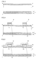
Fig. 3 ] A sectional view for illustrating a step of manufacturing the solar cell according to the first embodiment of the present invention. - [
Fig. 4 ] A sectional view for illustrating another step of manufacturing the solar cell according to the first embodiment of the present invention. - [
Fig. 5 ] A sectional view for illustrating still another step of manufacturing the solar cell according to the first embodiment of the present invention. - [
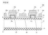
Fig. 6 ] A sectional view of a solar cell according to a second embodiment of the present invention. - [
Fig. 7 ] A sectional view of a solar cell according to a third embodiment of the present invention. - [
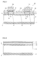
Fig. 8 ] A sectional view for illustrating a step of manufacturing the solar cell according to the third embodiment of the present invention. - [
Fig. 9 ] A sectional view for illustrating another step of manufacturing the solar cell according to the third embodiment of the present invention. - [
Fig. 10 ] A sectional view for illustrating still another step of manufacturing the solar cell according to the third embodiment of the present invention. - [
Fig. 11 ] A sectional view for illustrating a further step of manufacturing the solar cell according to the third embodiment of the present invention. - [
Fig. 12 ] A sectional view of a solar cell according to a fourth embodiment of the present invention. - [
Fig. 13 ] A sectional view for illustrating a step of manufacturing the solar cell according to the fourth embodiment of the present invention. - [
Fig. 14 ] A characteristic diagram showing the relation between an output of the solar cell according to the third embodiment and the thickness of a cap layer. - Embodiments of the present invention are now described with reference to the drawings. In the following description of the drawings, identical or similar reference numerals are assigned to identical or similar portions. However, it is to be noted that the drawings are schematic ones, and the ratios etc. of respective dimensions are different from the actual ones. Therefore, the specific dimensions etc. must be determined in consideration of the following description. Further, portions whose mutual dimensional relations and ratios are different from each other are also included in the drawings, as a matter of course.
- The structure of a
solar cell 100 according to a first embodiment of the present invention is described with reference toFigs. 1 and 2 . - As shown in
Figs. 1 and 2 , thesolar cell 100 is provided with asubstrate 10 made of a semiconductor. As shown inFig. 2 , thesubstrate 10 is a semiconductor substrate in the form of a thin plate, and has a p-type or n-type conductivity type. Thesubstrate 10 is made of crystalline silicon such as single-crystalline silicon or polycrystalline silicon, a compound semiconductor such as GaAs or InP, or still another semiconductor which can be formed in a plate shape. Thesubstrate 10 is an example of the "semiconductor substrate" in the present invention. - The
substrate 10 has a photoreceiving surface A and a back surface B. The photoreceiving surface A is a surface upon which light is incident. The back surface B is a surface opposite to the photoreceiving surface A. Both of the photoreceiving surface A and the back surface B are major surfaces of thesubstrate 10. The back surface B has a first region B1 and a second region B2. - Carriers are formed in the
substrate 10 due to the light incident upon the photoreceiving surface A. The carriers denote electrons and holes formed by the light absorbed by thesubstrate 10. - A light incidence-
side structure 15 is provided on the side of the photoreceiving surface A of thesubstrate 10 of thesolar cell 100. On the other hand, an i-typeamorphous semiconductor layer 11, a p-typeamorphous semiconductor layer 12a, an n-typeamorphous semiconductor layer 13a, a p-side electrode 20a and an n-side electrode 20b are provided on the side of the back surface B of thesubstrate 10 of thesolar cell 100. The i-typeamorphous semiconductor layer 11 is an example of the "third semiconductor layer" in the present invention, the p-typeamorphous semiconductor layer 12a is an example of the "first semiconductor layer" in the present invention, and the n-typeamorphous semiconductor layer 13a is an example of the "second semiconductor layer" in the present invention. - In a case where the
substrate 10 has n-type conductivity in the solar cell of this structure, a junction for forming an electric field for carrier separation is formed between thesubstrate 10 and the p-typeamorphous semiconductor layer 12a, while a junction for forming an electric field for preventing recombination of minority carriers is formed between thesubstrate 10 and the n-typeamorphous semiconductor layer 13a. In a case where thesubstrate 10 has p-type conductivity, a junction for forming an electric field for carrier separation is formed between thesubstrate 10 and the n-typeamorphous semiconductor layer 13a, while a junction for forming an electric field for preventing recombination of minority carriers is formed between thesubstrate 10 and the p-typeamorphous semiconductor layer 12a. - The light incidence-
side structure 15 is formed to transmit part of the incident light to the side of thesemiconductor substrate 10. Therefore, part of the incident light is transmitted through the light incidence-side structure 15 and incident upon the photoreceiving surface A of thesemiconductor substrate 10. The light transmittance of the light incidence-side structure 15 is preferably large, in order to increase the quantity of the light incident upon thesemiconductor substrate 10. Therefore, the light incidence-side structure 15 preferably includes no layer such as a metal layer, for example, having small light transmittance. - The light incidence-
side structure 15 is constituted of apassivation film 15a and anantireflective film 15b. The light incidence-side structure 15 is constituted of a single layer of an amorphous semiconductor layer, a silicon oxide layer or a silicon nitride layer, or a multilayer structure of such layers. The structure of the light incidence-side structure 15 is not restricted to this, but the light incidence-side structure 15 can take any structure. - The i-type
amorphous semiconductor layer 11 is formed substantially on the whole of the back surface B of thesubstrate 10. More specifically, the i-typeamorphous semiconductor layer 11 is formed on the first region B1 of the back surface B of thesubstrate 10 on which the p-typeamorphous semiconductor layer 12a is formed and the second region B2 adjacent to the first region B1. Further, the i-typeamorphous semiconductor layer 11 is formed between thesemiconductor substrate 10 and the p-type and n-typeamorphous semiconductor layers amorphous semiconductor layer 11 is formed in an atmosphere into which no p-type and n-type impurities are positively introduced. In other words, the i-typeamorphous semiconductor layer 11 has a substantially intrinsic conductivity type. The i-typeamorphous semiconductor layer 11, substantially containing no p-type and n-type impurities, may contain a small quantity. Also in a case where source gas contains no impurity, contamination with an impurity desorbing from a film adhering to a substrate tray or a chamber wall may take place, and a small quantity of impurity is contained in the i-typeamorphous semiconductor layer 11 in this case. The thickness of the i-typeamorphous semiconductor layer 11 is at a degree substantially not contributing to power generation, and about several nm to 25 nm, for example. - The p-type
amorphous semiconductor layer 12a is formed on the first region B1 of the back surface B of thesubstrate 10. According to the first embodiment, the p-typeamorphous semiconductor layer 12a is formed on the surface of the i-typeamorphous semiconductor layer 11 on the first region B1 of the back surface B of thesubstrate 10. The thickness of the p-typeamorphous semiconductor layer 12a is about 10 nm, for example. - The n-type
amorphous semiconductor layer 13a is formed substantially on the whole of the surface of the i-typeamorphous semiconductor layer 11. More specifically, the n-typeamorphous semiconductor layer 13a is formed to extend over the surface of the i-typeamorphous semiconductor layer 11 and the surface of acap layer 30 described later. - Each of the i-type
amorphous semiconductor layer 11, the p-typeamorphous semiconductor layer 12a and the n-typeamorphous semiconductor layer 13a is preferably made of a hydrogenated amorphous semiconductor containing silicon. As such an amorphous semiconductor, there is amorphous silicon, amorphous silicon carbide, or amorphous silicon germanium. The i-typeamorphous semiconductor layer 11, the p-typeamorphous semiconductor layer 12a and the n-typeamorphous semiconductor layer 13a are not restricted to this material, but may be made of another amorphous semiconductor, and not restricted to the amorphous semiconductor, but may be made of another thin-film semiconductor. - Further, the i-type
amorphous semiconductor layer 11, the p-typeamorphous semiconductor layer 12a and the n-typeamorphous semiconductor layer 13a are not restricted to such ones that the overall layers are in complete amorphous states, but may partially have crystalline regions. For example, the layers may be those of the so-called microcrystalline states containing large numbers of small crystalline regions therein. In addition, the i-typeamorphous semiconductor layer 11, the p-typeamorphous semiconductor layer 12a and the n-typeamorphous semiconductor layer 13a may be single layers, or multilayers. - The p-
side electrode 20a is an electrode collecting carriers. The p-side electrode 20a is formed on the p-typeamorphous semiconductor layer 12a while holding the n-typeamorphous semiconductor layer 13a therebetween. Therefore, the p-side electrode 20a is formed on the first region B1 of the back surface B of thesubstrate 10. - The n-
side electrode 20b is an electrode collecting carriers. The n-side electrode 20b is formed on the second region B2 of the back surface B of thesubstrate 10 while holding the n-typeamorphous semiconductor layer 13a therebetween. Further, the n-side electrode 20b is formed on the surface of the n-typeamorphous semiconductor layer 13a on the second region B2 of the back surface B of thesubstrate 10. - The p-
side electrode 20a and the n-side electrode 20b are made of a metallic material or a conductive paste material. Further, the p-side electrode 20a and the n-side electrode 20b are formed by any method such as sputtering, vapor deposition, plating or printing. - According to the first embodiment, the
cap layer 30 is formed between the p-typeamorphous semiconductor layer 12a and the n-typeamorphous semiconductor layer 13a. More specifically, thecap layer 30 is formed between the upper surface of the p-typeamorphous layer 12a and the n-typeamorphous semiconductor layer 13a. Thecap layer 30 is so formed that the thickness thereof is smaller than the thicknesses of the p-typeamorphous semiconductor layer 12a and the n-typeamorphous semiconductor layer 13a. Further, thecap layer 30 is formed to inhibit the p-type impurity from desorbing from the p-typeamorphous semiconductor layer 12a serving as an underlayer. - The
cap layer 30 is made of a semiconductor or an insulator substantially containing no impurity for doping contained in the semiconductor layer serving as the underlayer. Thecap layer 30, substantially containing no impurity, may contain a small quantity of impurity. Also in a case where source gas contains no impurity, contamination with an impurity desorbing from a film adhering to a substrate tray or a chamber wall may take place, and a small quantity of impurity is contained in thecap layer 30 in this case. According to the first embodiment, thecap layer 30 is made of the material containing no p-type impurity, whereby no p-type impurity desorbs from thecap layer 30 by plasma for forming the n-typeamorphous semiconductor layer 13a. Therefore, thecap layer 30 can inhibit the p-type impurity from desorbing from the p-typeamorphous semiconductor layer 12a by the plasma for forming the n-typeamorphous semiconductor layer 13a. Thus, the space between thesubstrate 10 and the n-typeamorphous semiconductor layer 13a can be inhibited from contamination with an unintended p-type impurity, whereby solar cell characteristics can be improved. - The
cap layer 30 is preferably made of a material containing no n-type impurity. In other words, thecap layer 30 is preferably made of a material containing neither a p-type impurity nor an n-type impurity. In this case, a p-type impurity and an n-type impurity can be inhibited from desorbing from thecap layer 30 by the plasma for forming the n-typeamorphous semiconductor layer 13a. Further, thecap layer 30 can prevent the p-type impurity from desorbing from the p-typeamorphous semiconductor layer 12a by the plasma for forming the n-typeamorphous semiconductor layer 13a. Therefore, thecap layer 30 can inhibit undesired p-type impurity and n-type impurity from being contained in the space between thesubstrate 10 and the n-typeamorphous semiconductor layer 13a. Thus, the junction between thesubstrate 10 and the n-typeamorphous semiconductor layer 13a can be formed as designed, whereby the solar cell characteristics can be further improved. - The
cap layer 30 preferably contains no impurity exerting a remarkable bad influence on the semiconductor layer serving as the underlayer. For example, thecap layer 30 preferably contains neither organic matter nor an alkaline component. Even if part of the constituent element desorbs from thecap layer 30 by the plasma for forming the n-type amorphous semiconductor layer 13 in this case, the desorbing element can be inhibited from exerting a bad influence on the semiconductor layer serving as the underlayer. Thus, reduction of junction characteristics between thesubstrate 10 and the n-typeamorphous semiconductor layer 13a can be suppressed, whereby the solar cell characteristics can be excellently maintained. - The
cap layer 30 is preferably made of the same semiconductor material as the semiconductor layer serving as the underlayer. For example, the underlayer is the p-typeamorphous semiconductor layer 12a in the first embodiment, and hence thecap layer 30 is preferably made of an amorphous semiconductor material. Thecap layer 30 made of an amorphous semiconductor can be formed under conditions similar to those for the p-typeamorphous semiconductor layer 12a. Thus, the p-typeamorphous semiconductor layer 12a can be inhibited from being excessively influenced by an atmosphere at the time of forming thecap layer 30. Further, reduction of the characteristics of the p-typeamorphous semiconductor layer 12a can be suppressed, whereby further improvement of the solar cell characteristics can be attained. - Further, the
cap layer 30 is preferably made of an inorganic insulator such as a metal oxide such as silicon oxide or a metal nitride such as silicon nitride. When thecap layer 30 is made of an inorganic insulator, a p-type impurity and an n-type impurity can be inhibited from desorbing from thecap layer 30 by the plasma for forming the n-typeamorphous semiconductor layer 13a. The inorganic insulator has higher plasma resistance as compared with the semiconductor material, whereby desorption of the constituent element of thecap layer 30 can also be suppressed. Therefore, thecap layer 30 can inhibit undesired impurities such as a p-type impurity and an n-type impurity from being contained in the space between thesubstrate 10 and the n-typeamorphous semiconductor layer 13a. Thus, the junction between thesubstrate 10 and the n-typeamorphous semiconductor layer 13a can be formed as designed, whereby the solar cell characteristics can be further improved. - A method of manufacturing the
solar cell 100 according to the first embodiment is now described with reference toFigs. 3 to 5 . - First, an n-type single-crystalline silicon substrate in which a textured structure is previously formed on the photoreceiving surface A is prepared as the
substrate 10. - Then, the
passivation film 15a consisting of an i-type amorphous silicon layer having a thickness of 3 nm to 5 nm is formed substantially on the whole of the photoreceiving surface A of thesubstrate 10 by CVD, and theantireflective film 15b consisting of a layer of a silicon nitride having a thickness of 50 nm to 150 nm is further successively stacked by CVD, as shown inFig. 3 . The light incidence-side structure 15 is constituted of thepassivation film 15a and theantireflective film 15b. Thepassivation film 15a contains hydrogen, and hence the same has a function of passivating thesubstrate 10. Theantireflective film 15b has an antireflective function. The multilayer structure of the i-type amorphous silicon layer and the silicon nitride layer is an example of the light incidence-side structure 15. - Then, the i-type
amorphous semiconductor layer 11 made of i-type amorphous silicon having a thickness of 3 nm to 50 nm is formed substantially on the whole of the back surface B of thesubstrate 10 by CVD. The i-typeamorphous semiconductor layer 11 contains hydrogen, and hence the same has a function of passivating thesubstrate 10. - Then, the p-type
amorphous semiconductor layer 12a made of p-type amorphous silicon having a thickness of 2 nm to 50 nm and thecap layer 30 made of i-type amorphous silicon having a thickness of 0.5 nm to 5 nm are successively formed on the surface of the i-typeamorphous semiconductor layer 11 in a prescribed pattern by CVD employing a mask, as shown inFig. 4 . The prescribed pattern is a pattern corresponding to the first region B1 of the back surface B of thesubstrate 10. - Further, the n-type
amorphous semiconductor layer 13a made of n-type amorphous silicon having a thickness of 2 nm to 50 nm is formed by CVD to extend over the surface of the i-typeamorphous semiconductor layer 11 and the surface of thecap layer 30, as shown inFig. 5 . - Finally, the p-
side electrode 20a and the n-side electrode 20b are formed on the surface of the n-typeamorphous semiconductor layer 13a in prescribed patterns by a method such as sputtering or printing. Thus, thesolar cell 100 according to the first embodiment is manufactured. - In the
solar cell 100 according to the first embodiment, thecap layer 30 is formed between the upper surface of the p-typeamorphous semiconductor layer 12a and the n-typeamorphous semiconductor layer 13a. Thecap layer 30 is formed to suppress desorption of the impurity for doping contained in the p-typeamorphous semiconductor layer 12a serving as the underlayer. Thus, the space between thesubstrate 10 and the n-typeamorphous semiconductor layer 13a can be inhibited from contamination with the undesired impurity for doping. More specifically, the space between the surface of the i-typeamorphous semiconductor layer 11 and the surface of the n-typeamorphous semiconductor layer 13a can be inhibited from contamination with the undesired p-type impurity on the second region B2 of the back surface B of thesubstrate 10. In other words, junction characteristics between thesubstrate 10 and the n-typeamorphous semiconductor layer 13a can be excellently maintained, whereby a solar cell having excellent solar cell characteristics can be provided. - A
solar cell 150 according to a second embodiment of the present invention is now described with reference toFig. 6 . - As shown in
Fig. 6 , acap layer 31 is formed between the upper surface and the side surfaces of a p-typeamorphous semiconductor layer 12a and an n-typeamorphous semiconductor layer 13a in thesolar cell 150 according to the second embodiment. The remaining structure of the second embodiment is similar to that of the aforementioned first embodiment. - A method of manufacturing the
solar cell 150 according to the second embodiment is now described. - First, a light incidence-
side structure 15 is formed substantially on the whole of a photoreceiving surface A of asubstrate 10, similarly to the first embodiment. Further, an i-typeamorphous semiconductor layer 11 is formed substantially on the whole of a back surface B of thesubstrate 10 by CVD. Then, the p-typeamorphous semiconductor layer 12a is formed on the surface of the i-typeamorphous semiconductor layer 11 in a prescribed pattern. - According to the second embodiment, the
cap layer 31 made of i-type silicon is formed on the upper surface and the side surfaces of the p-typeamorphous semiconductor layer 12a. Then, an n-typeamorphous semiconductor layer 13a is formed to extend over the surface of the i-typeamorphous semiconductor layer 11 and the surface of thecap layer 31. - Finally, a p-
side electrode 20a and an n-side electrode 20b are formed on the surface of the n-typeamorphous semiconductor layer 13a in prescribed patterns, similarly to the first embodiment. Thus, thesolar cell 150 according to the second embodiment is manufactured. - According to the second embodiment, the
cap layer 31 containing no p-type impurity is formed not only between the upper surface of the p-typeamorphous semiconductor layer 12a and the n-typeamorphous semiconductor layer 13a but also between the side surfaces of the p-typeamorphous semiconductor layer 12a and the n-typeamorphous semiconductor layer 13a, whereby the space between thesubstrate 10 and the n-typeamorphous semiconductor layer 13a can be further inhibited from contamination with an undesired p-type impurity. - A
solar cell 200 according to a third embodiment of the present invention is now described with reference toFigs. 7 to 11 . In the following, points different from those of the first embodiment are mainly described. -
Fig. 7 is a sectional view of thesolar cell 200 according to the third embodiment of the present invention. As shown inFig. 7 , an i-typeamorphous semiconductor layer 12b and a p-typeamorphous semiconductor layer 12a are successively stacked on the surface of a first region B1 of a back surface B of asubstrate 10. In other words, the i-typeamorphous semiconductor layer 12b is formed between thesemiconductor substrate 10 and the p-typeamorphous semiconductor layer 12a. Acap layer 30 is formed on the upper surface of the p-typeamorphous semiconductor layer 12a. An i-typeamorphous semiconductor layer 13b and a p-typeamorphous semiconductor layer 13a are stacked to extend over the back surface B (a second region B2 adjacent to the first region B1 on which the p-typeamorphous semiconductor layer 12a is formed) of thesubstrate 10 and the surface of thecap layer 30. The i-typeamorphous semiconductor layer 12b is an example of the "fourth semiconductor layer" in the present invention, and the i-typeamorphous semiconductor layer 13b is an example of the "fifth semiconductor layer" in the present invention. According to the third embodiment, the "third semiconductor layer" in the present invention is constituted of the i-typeamorphous semiconductor layer 12b and the i-typeamorphous semiconductor layer 13b. - A method of manufacturing the
solar cell 200 according to the third embodiment is now described with reference toFigs. 8 to 11 . - First, the
substrate 10 made of n-type single-crystalline silicon in which a textured structure is previously formed on the photoreceiving surface A is prepared, similarly to the first embodiment. Then, a light incidence-side structure 15 is formed substantially on the whole of the photoreceiving surface A of thesubstrate 10, as shown inFig. 8 . - Then, the i-type
amorphous semiconductor layer 12b made of i-type amorphous silicon having a thickness of 3 nm to 50 nm, the p-typeamorphous semiconductor layer 12a having a thickness of 2 nm to 50 nm and thecap layer 30 having a thickness of 0.5 nm to 5 nm are successively formed substantially on the whole of a back surface B of thesubstrate 10 by CVD. Thecap layer 30 is formed without positively introducing p-type and n-type impurities for doping. - Then, a resist
film 40 is formed on the surface of thecap layer 30 in a prescribed pattern, as shown inFig. 9 . The prescribed pattern is a pattern corresponding to the pattern of the first region B1 on the back surface B of thesubstrate 10. - Then, portions of the i-type
amorphous semiconductor layer 12b, the p-typeamorphous semiconductor layer 12a and thecap layer 30 exposed from the resistfilm 40 are removed by etching, and the resistfilm 40 is thereafter removed, as shown inFig. 10 . A multilayer film of the i-typeamorphous semiconductor layer 12b, the p-typeamorphous semiconductor layer 12a and thecap layer 30 is formed on the surface of the first region B1 on the back surface B of thesubstrate 10 through this step. - While
Fig. 10 shows an example of removing the multilayer film of the i-typeamorphous semiconductor layer 12b, the p-typeamorphous semiconductor layer 12a and thecap layer 30 until the back surface B of thesubstrate 10 is exposed, the same may be removed by etching to expose the i-typeamorphous semiconductor layer 12b. In this step, at least the p-type amorphous semiconductor layer 12 may be removed, and part of the i-typeamorphous semiconductor layer 12b may remain on the back surface B of thesubstrate 10. - Then, the i-type
amorphous semiconductor layer 13b made of i-type amorphous silicon having a thickness of 3 nm to 50 nm and the n-typeamorphous semiconductor layer 13a having a thickness of 2 nm to 50 nm are successively formed by CVD to extend over the surface of the back surface B of thesubstrate 10 and the surface of thecap layer 30, as shown inFig. 11 . More specifically, the i-typeamorphous semiconductor layer 13b and the n-typeamorphous semiconductor layer 13a are formed substantially on the whole of the back surface B of thesubstrate 10. - Finally, a p-
side electrode 20a and an n-side electrode 20b are formed on the surface of the n-typeamorphous semiconductor layer 13a in prescribed patterns by a method such as sputtering or printing. Thus, thesolar cell 200 according to the third embodiment is manufactured. - In the
solar cell 200 according to the third embodiment, an undesired doping impurity can be inhibited from being contained in the space between thesubstrate 10 and the n-typeamorphous semiconductor layer 13a by thecap layer 30 similarly to the first embodiment, whereby solar cell characteristics can be improved. - A
solar cell 250 according to a fourth embodiment of the present invention is now described with reference toFigs. 12 and13 . - In the
solar cell 250 according to the fourth embodiment, acap layer 32 is made of an insulator, as shown inFig. 12 . More specifically, thecap layer 32 is made of an insulating material such as a metal oxide or a metal nitride. Further, acontact hole 50 is formed in an n-typeamorphous semiconductor layer 13a, an i-typeamorphous semiconductor layer 13b and thecap layer 32. A p-side electrode layer 20c is formed to be in contact with a p-typeamorphous semiconductor layer 12a through thecontact hole 50. More specifically, the p-side electrode layer 20c is formed to fill up thecontact hole 50. The remaining structure of the fourth embodiment is similar to that of the aforementioned third embodiment. - A method of manufacturing the
solar cell 250 according to the fourth embodiment is now described with reference toFig. 13 . - First, a light incidence-
side structure 15 is formed substantially on the whole of a photoreceiving surface A of asubstrate 10, similarly to the third embodiment. Then, an i-typeamorphous semiconductor layer 12b, the p-typeamorphous semiconductor layer 12a, thecap layer 32, the i-typeamorphous semiconductor layer 13b and the n-typeamorphous semiconductor layer 13a are successively formed on a back surface B of thesubstrate 10. According to the fourth embodiment, thecap layer 32 is made of the insulating material such as a metal oxide or a metal nitride, dissimilarly to the third embodiment. - According to the fourth embodiment, the
contact hole 50 is formed in the n-typeamorphous semiconductor layer 13a, the i-typeamorphous semiconductor layer 13b and thecap layer 32 by etching, as shown inFig. 13 . Then, the p-side electrode layer 20c is formed to be in contact with the p-typeamorphous semiconductor layer 12a through thecontact hole 50. More specifically, the p-side electrode layer 20c is formed to fill up thecontact hole 50. - Then, an n-
side electrode 20b is formed on the surface of the n-typeamorphous semiconductor layer 13a in a prescribed pattern, similarly to the third embodiment. Thus, thesolar cell 250 according to the fourth embodiment is manufactured. - In the
solar cell 250 according to the fourth embodiment, thecap layer 32 is made of the insulating material such as a metal oxide or a metal nitride. In thesolar cell 250, further, thecontact hole 50 is formed in the n-typeamorphous semiconductor layer 13a, the i-typeamorphous semiconductor layer 13b andcap layer 32, and the p-side electrode layer 20c is formed to fill up thecontact hole 50. Thus, the p-side electrode layer 20c can be brought into direct contact with the p-typeamorphous semiconductor layer 12a, whereby collection efficiency for carriers can be improved. - The embodiments disclosed this time must be considered as illustrative in all points and not restrictive. The range of the present invention is shown not by the above description of the embodiments but by the scope of claims for patent, and all modifications within the meaning and range equivalent to the scope of claims for patent are included.
- For example, while the p-type
amorphous semiconductor layer 12a and thecap layer 30 have been formed on the first region B1 of the back surface B of thesubstrate 10 and the n-typeamorphous semiconductor layer 13a has been formed to extend over the second region B2 of the back surface B of thesubstrate 10 and the surface of thecap layer 30 in each of the first to third embodiments, the arrangement relation between the p-typeamorphous semiconductor layer 12a and the n-typeamorphous semiconductor layer 13a may be reversed thereto. In other words, the n-typeamorphous semiconductor layer 13a and thecap layer 30 may be formed on the first region B1 of the back surface B of thesubstrate 10, and the p-typeamorphous semiconductor layer 12a may be formed to extend over the second region B2 of the back surface B of thesubstrate 10 and the surface of thecap layer 30. Also in such a structure, the space between the surface of thesubstrate 10 and the p-typeamorphous semiconductor layer 12a can be inhibited from contamination with an undesired n-type impurity by thecap layer 30, whereby a solar cell having excellent solar cell characteristics can be provided. - Example of the present invention is now described. In this Example, the
solar cell 200 shown inFig. 7 was manufactured as follows: - First, anisotropic etching was performed on a
substrate 10 made of n-type single-crystalline silicon having a thickness of about 200 µm, and textured structures were formed on a photoreceiving surface A and a back surface B of thesubstrate 10. - Then, an i-type
amorphous semiconductor layer 15a made of i-type amorphous silicon having a thickness of 10 nm was formed on the photoreceiving surface A of thesubstrate 10 by plasma CVD, by employing mixed gas of SiH4 and H2 as source gas. - Then, an i-type
amorphous silicon layer 12b having a thickness of 20 nm, a p-typeamorphous semiconductor layer 12a made of p-type amorphous silicon having a thickness of 10 nm and acap layer 30 made of i-type amorphous silicon were successively formed on a first region B1 of the back surface B of thesubstrate 10 by plasma CVD, by employing SiH4, H2 and B2H6 as source gas. In this Example, the i-typeamorphous semiconductor layer 12b, the p-typeamorphous semiconductor layer 12a and thecap layer 30 were formed in prescribed patterns by employing a mask. When forming thecap layer 30, the thickness of thecap layer 30 was varied to 0.5 nm, 1 nm, 1.5 nm, 2 nm, 2.5 nm, 3 nm, 3.5 nm, 4 nm, 4.5 nm, 5 nm, 6 nm, 7 nm and 8 nm, for manufacturing 13 samples in which the thicknesses of cap layers 30 were different from each other. - Then, an i-type
amorphous semiconductor layer 13b made of i-type amorphous silicon having a thickness of 3 nm and an n-typeamorphous semiconductor layer 13a made of n-type amorphous silicon having a thickness of 20 nm were successively formed by plasma CVD to extend over the surface of a second region B2 of the back surface B of thesubstrate 10 and the surface of thecap layer 30, by employing SiH4, H2 and PH3 as source gas. The formation of the i-typeamorphous semiconductor layer 13b was performed while setting the quantity of introduction of PH3 to zero. - Finally, a p-
side electrode 20a and an n-side electrode 20b were pattern-formed by printing. - Example samples were manufactured in the aforementioned manner.
- As a comparative example sample, a comparative example sample was manufactured similarly to the aforementioned Example, except that no
cap layer 30 was provided. - Results of measuring solar cell characteristics are now described with reference to the Example samples and the comparative example sample.
-
Fig. 14 is a characteristic diagram showing the results of measuring the solar cell characteristics as to the Example samples and the comparative example sample. The axis of ordinates of the drawing shows relative values of outputs of the solar cells, which are values standardized on the assumption that the output of the comparative example sample in which the thickness of thecap layer 30 was 0 nm was 1. The axis of abscissas shows the thicknesses (nm) of the cap layers 30. - As shown in
Fig. 14 , it is understood that the solar cell characteristics are improved by providing thecap layer 30. This is conceivably because it was possible to inhibit an undesired doping impurity from being contained in the space between thesubstrate 10 and the n-typeamorphous semiconductor layer 13a by providing thecap layer 30. - Further, it is understood that the output is improved as compared with the comparative example sample if the
cap layer 30 simply has a slight thickness. Therefore, the thickness of thecap layer 30 may simply be at least several nm. - In addition, it was understood that the output is improved as compared with the comparative example sample by setting the thickness of the
cap layer 30 to not more than 5 nm. If the thickness of thecap layer 30 is greater than 5 nm, the output lowers as compared with the comparative example sample. The reason why the output lowers in this manner is conceivably because resistance between the p-side electrode 20a and the p-type amorphous silicon layer 12 increased by increasing the thickness of thecap layer 30. - Therefore, the thickness of the cap layer is preferably in the range of at least several nm and not more than 5 nm, more preferably in the range of at least 0.5 nm and not more than 4 nm, and further preferably in the range of at least 1.5 nm and not more than 3.5 nm.
Claims (20)
- A solar cell (100, 150, 200, 250) comprising:a semiconductor substrate (10) having a photoreceiving surface and a back surface;a first semiconductor layer (12a) of a first conductivity type formed on a prescribed region of the back surface of said semiconductor substrate;a second semiconductor layer (13a) of a second conductivity type formed to extend over the back surface of said semiconductor substrate and the surface of said first semiconductor layer; anda cap layer (30, 31, 32), formed between said first semiconductor layer and said second semiconductor layer, made of a semiconductor or an insulator substantially containing no impurity of said first conductivity type.
- The solar cell according to claim 1, wherein
said cap layer is formed between at least the upper surface of said first semiconductor layer and said second semiconductor layer. - The solar cell according to claim 2, wherein
said cap layer is formed between the upper surface and the side surface of said first semiconductor layer and said second semiconductor layer. - The solar cell according to claim 1, wherein
said cap layer is made of a semiconductor. - The solar cell according to claim 1, wherein
said cap layer is made of an insulator. - The solar cell according to claim 5, wherein
said second semiconductor layer and said cap layer include a contact hole (50), and
the solar cell further comprises an electrode layer (20c) formed to be in contact with the first semiconductor layer through said contact hole. - The solar cell according to claim 1, wherein
the thickness of said cap layer is smaller than the thicknesses of said first semiconductor layer and said second semiconductor layer. - The solar cell according to claim 1, further comprising a substantially intrinsic third semiconductor layer (11) formed between said semiconductor substrate and said first and second semiconductor layers.
- The solar cell according to claim 8, wherein
said third semiconductor layer is formed on said prescribed region of the back surface of said semiconductor substrate on which said first semiconductor layer is formed and a region adjacent to said prescribed region, and
said second semiconductor layer is formed to extend over the surface of said third semiconductor layer and the surface of said cap layer. - The solar cell according to claim 8, wherein
said third semiconductor layer includes a fourth semiconductor layer (12b) formed on said prescribed region of the back surface of said semiconductor substrate on which said first semiconductor layer is formed. - The solar cell according to claim 10, wherein
said third semiconductor layer further includes a fifth semiconductor layer (13b) formed to extend over a region adjacent to said prescribed region of the back surface of said semiconductor substrate on which said first semiconductor layer is formed and the surface of said cap layer. - The solar cell according to claim 8, wherein
said third semiconductor layer is an amorphous semiconductor layer. - The solar cell according to claim 1, wherein
said cap layer is made of the same semiconductor material as said first semiconductor layer. - The solar cell according to claim 1, wherein
said cap layer contains neither an impurity of said first conductivity type nor an impurity of said second conductivity type. - The solar cell according to claim 14, wherein
said cap layer is an intrinsic amorphous semiconductor layer. - The solar cell according to claim 1, wherein
said semiconductor substrate is a crystalline semiconductor substrate. - The solar cell according to claim 16, wherein
said semiconductor substrate is a single-crystalline semiconductor substrate of the second conductivity type. - The solar cell according to claim 1, further comprising a light incidence-side structure (15) formed on the photoreceiving surface of said semiconductor substrate.
- The solar cell according to claim 18, wherein
said light incidence-side structure includes at least an antireflective film (15b). - The solar cell according to claim 19, wherein
said light incidence-side structure includes a passivation film (15a), in addition to said antireflective film.
Applications Claiming Priority (2)
| Application Number | Priority Date | Filing Date | Title |
|---|---|---|---|
| JP2009081023 | 2009-03-30 | ||
| PCT/JP2010/055195 WO2010113750A1 (en) | 2009-03-30 | 2010-03-25 | Solar cell |
Publications (3)
| Publication Number | Publication Date |
|---|---|
| EP2416373A1 true EP2416373A1 (en) | 2012-02-08 |
| EP2416373A4 EP2416373A4 (en) | 2016-11-02 |
| EP2416373B1 EP2416373B1 (en) | 2019-12-25 |
Family
ID=42828043
Family Applications (1)
| Application Number | Title | Priority Date | Filing Date |
|---|---|---|---|
| EP10758523.4A Active EP2416373B1 (en) | 2009-03-30 | 2010-03-25 | Solar cell |
Country Status (9)
| Country | Link |
|---|---|
| US (1) | US8796539B2 (en) |
| EP (1) | EP2416373B1 (en) |
| JP (1) | JP5383792B2 (en) |
| KR (1) | KR101521326B1 (en) |
| CN (1) | CN102369601B (en) |
| BR (1) | BRPI1009416A2 (en) |
| MY (1) | MY152718A (en) |
| SG (1) | SG175041A1 (en) |
| WO (1) | WO2010113750A1 (en) |
Cited By (5)
| Publication number | Priority date | Publication date | Assignee | Title |
|---|---|---|---|---|
| WO2014001885A1 (en) * | 2012-06-29 | 2014-01-03 | Rec Cells Pte. Ltd. | Method for fabricating a rear contact heterojunction intrinsic thin layer silicon solar cell with only two masking steps and respective solar cell |
| NL2010496C2 (en) * | 2013-03-21 | 2014-09-24 | Stichting Energie | Solar cell and method for manufacturing such a solar cell. |
| US9761749B2 (en) | 2011-10-05 | 2017-09-12 | Semiconductor Energy Laboratory Co., Ltd. | Photoelectric conversion device |
| EP3223318A1 (en) * | 2016-03-23 | 2017-09-27 | Meyer Burger (Germany) AG | Hetero junction photovoltaic cell and method of manufacturing same |
| EP2660873A4 (en) * | 2010-12-29 | 2018-03-28 | Panasonic Intellectual Property Management Co., Ltd. | Method for manufacturing solar cell and solar cell |
Families Citing this family (86)
| Publication number | Priority date | Publication date | Assignee | Title |
|---|---|---|---|---|
| WO2010113750A1 (en) * | 2009-03-30 | 2010-10-07 | 三洋電機株式会社 | Solar cell |
| JP5485060B2 (en) * | 2010-07-28 | 2014-05-07 | 三洋電機株式会社 | Manufacturing method of solar cell |
| JP5334926B2 (en) * | 2010-08-02 | 2013-11-06 | 三洋電機株式会社 | Manufacturing method of solar cell |
| JP5388970B2 (en) * | 2010-08-24 | 2014-01-15 | 三洋電機株式会社 | Manufacturing method of solar cell |
| JP5595850B2 (en) * | 2010-09-27 | 2014-09-24 | 三洋電機株式会社 | Manufacturing method of solar cell |
| JPWO2012132835A1 (en) | 2011-03-25 | 2014-07-28 | 三洋電機株式会社 | Solar cell |
| WO2012132064A1 (en) * | 2011-03-25 | 2012-10-04 | 三洋電機株式会社 | Photovoltaic element |
| EP2690667A4 (en) * | 2011-03-25 | 2014-10-08 | Sanyo Electric Co | METHOD FOR PRODUCING PHOTOELECTRIC CONVERSION DEVICE |
| WO2012132613A1 (en) * | 2011-03-25 | 2012-10-04 | 三洋電機株式会社 | Method for producing photoelectric conversion element |
| WO2012132616A1 (en) * | 2011-03-25 | 2012-10-04 | 三洋電機株式会社 | Method for producing photoelectric conversion element |
| WO2012132655A1 (en) * | 2011-03-25 | 2012-10-04 | 三洋電機株式会社 | Back-junction photoelectric conversion element and method for manufacturing back-junction photoelectric conversion element |
| JP5879538B2 (en) * | 2011-03-25 | 2016-03-08 | パナソニックIpマネジメント株式会社 | Photoelectric conversion device and manufacturing method thereof |
| WO2012132654A1 (en) * | 2011-03-25 | 2012-10-04 | 三洋電機株式会社 | Back-junction photoelectric conversion element and method for manufacturing back-junction photoelectric conversion element |
| WO2012132961A1 (en) * | 2011-03-25 | 2012-10-04 | 三洋電機株式会社 | Method for producing photoelectric conversion element |
| JPWO2012132758A1 (en) * | 2011-03-28 | 2014-07-28 | 三洋電機株式会社 | Photoelectric conversion device and method of manufacturing photoelectric conversion device |
| WO2012132729A1 (en) * | 2011-03-28 | 2012-10-04 | 三洋電機株式会社 | Photoelectric conversion device and method for producing same |
| JP5842173B2 (en) * | 2011-03-28 | 2016-01-13 | パナソニックIpマネジメント株式会社 | Photoelectric conversion device and method of manufacturing photoelectric conversion device |
| JP2012204764A (en) * | 2011-03-28 | 2012-10-22 | Sanyo Electric Co Ltd | Solar cell and method for manufacturing the same |
| JPWO2012132766A1 (en) * | 2011-03-28 | 2014-07-28 | 三洋電機株式会社 | Photoelectric conversion device and method of manufacturing photoelectric conversion device |
| JPWO2012132834A1 (en) * | 2011-03-28 | 2014-07-28 | 三洋電機株式会社 | Solar cell and method for manufacturing solar cell |
| US9012769B2 (en) * | 2011-05-25 | 2015-04-21 | Semiconductor Energy Laboratory Co., Ltd. | Photoelectric conversion device |
| JP2013030615A (en) * | 2011-07-28 | 2013-02-07 | Sanyo Electric Co Ltd | Solar cell |
| JP5892584B2 (en) * | 2011-09-26 | 2016-03-23 | デクセリアルズ株式会社 | Solar cell module and method for manufacturing solar cell module |
| US8597970B2 (en) * | 2011-12-21 | 2013-12-03 | Sunpower Corporation | Hybrid polysilicon heterojunction back contact cell |
| JP6208682B2 (en) * | 2011-12-21 | 2017-10-04 | サンパワー コーポレイション | Hybrid polysilicon heterojunction back contact battery |
| FR2985608B1 (en) * | 2012-01-05 | 2016-11-18 | Commissariat Energie Atomique | PHOTOVOLTAIC CELL AND METHOD OF MAKING SAME |
| JP2013168605A (en) * | 2012-02-17 | 2013-08-29 | Sharp Corp | Manufacturing method of solar cell |
| WO2013133005A1 (en) * | 2012-03-08 | 2013-09-12 | 三洋電機株式会社 | Semiconductor device manufacturing method |
| KR20140019099A (en) * | 2012-08-02 | 2014-02-14 | 삼성에스디아이 주식회사 | Photoelectric device |
| JP6042679B2 (en) * | 2012-09-26 | 2016-12-14 | シャープ株式会社 | Photoelectric conversion element and method for producing photoelectric conversion element |
| WO2014136715A1 (en) * | 2013-03-04 | 2014-09-12 | シャープ株式会社 | Photoelectric conversion element |
| JP2014183073A (en) * | 2013-03-18 | 2014-09-29 | Sharp Corp | Photoelectric conversion element and method of manufacturing photoelectric conversion element |
| WO2014157525A1 (en) * | 2013-03-28 | 2014-10-02 | シャープ株式会社 | Photoelectric conversion element |
| JP6284522B2 (en) * | 2013-03-28 | 2018-02-28 | シャープ株式会社 | Photoelectric conversion element, photoelectric conversion module, and photovoltaic power generation system |
| CN104112789B (en) * | 2013-04-17 | 2016-04-27 | 茂迪股份有限公司 | Solar cell and manufacturing method thereof |
| JP6206843B2 (en) * | 2013-09-09 | 2017-10-04 | パナソニックIpマネジメント株式会社 | Solar cell |
| JP6404825B2 (en) * | 2013-10-25 | 2018-10-17 | シャープ株式会社 | Photoelectric conversion element |
| JPWO2015060013A1 (en) * | 2013-10-25 | 2017-03-09 | シャープ株式会社 | Photoelectric conversion element |
| JP2015109948A (en) * | 2013-10-31 | 2015-06-18 | キヤノン株式会社 | Subject information acquisition device |
| JP2015177175A (en) * | 2014-03-18 | 2015-10-05 | シャープ株式会社 | Photoelectric conversion element and method for producing photoelectric conversion element |
| JPWO2015189878A1 (en) * | 2014-06-13 | 2017-04-20 | 国立大学法人福島大学 | Solar cell and manufacturing method thereof |
| JP5957102B2 (en) * | 2015-01-21 | 2016-07-27 | シャープ株式会社 | Manufacturing method of solar cell |
| US10854767B2 (en) * | 2015-03-31 | 2020-12-01 | Kaneka Corporation | Solar cell and method for manufacturing same |
| US10505055B2 (en) * | 2015-08-31 | 2019-12-10 | Sharp Kabushiki Kaisha | Photoelectric conversion element |
| EP3365920B1 (en) * | 2015-10-25 | 2023-02-22 | Solaround Ltd. | Method of bifacial cell fabrication |
| EP3163632A1 (en) | 2015-11-02 | 2017-05-03 | CSEM Centre Suisse d'Electronique et de Microtechnique SA - Recherche et Développement | Photovoltaic device and method for manufacturing the same |
| CN109155342A (en) * | 2016-05-23 | 2019-01-04 | 株式会社钟化 | Solar cell, method for manufacturing the same, and solar cell panel |
| CN110047965A (en) * | 2018-01-16 | 2019-07-23 | 福建金石能源有限公司 | A kind of novel back contacts hetero-junction solar cell and preparation method thereof |
| US10824584B1 (en) | 2018-04-03 | 2020-11-03 | Xilinx, Inc. | Device with data processing engine array that enables partial reconfiguration |
| US10579559B1 (en) | 2018-04-03 | 2020-03-03 | Xilinx, Inc. | Stall logic for a data processing engine in an integrated circuit |
| US11016822B1 (en) | 2018-04-03 | 2021-05-25 | Xilinx, Inc. | Cascade streaming between data processing engines in an array |
| US11567881B1 (en) | 2018-04-03 | 2023-01-31 | Xilinx, Inc. | Event-based debug, trace, and profile in device with data processing engine array |
| US10990552B1 (en) | 2018-04-03 | 2021-04-27 | Xilinx, Inc. | Streaming interconnect architecture for data processing engine array |
| US11061673B1 (en) | 2018-04-03 | 2021-07-13 | Xilinx, Inc. | Data selection network for a data processing engine in an integrated circuit |
| US11113223B1 (en) | 2018-04-03 | 2021-09-07 | Xilinx, Inc. | Dual mode interconnect |
| US10747690B2 (en) | 2018-04-03 | 2020-08-18 | Xilinx, Inc. | Device with data processing engine array |
| US10866753B2 (en) | 2018-04-03 | 2020-12-15 | Xilinx, Inc. | Data processing engine arrangement in a device |
| US11372803B2 (en) | 2018-04-03 | 2022-06-28 | Xilinx, Inc. | Data processing engine tile architecture for an integrated circuit |
| US10635622B2 (en) | 2018-04-03 | 2020-04-28 | Xilinx, Inc. | System-on-chip interface architecture |
| US10747531B1 (en) | 2018-04-03 | 2020-08-18 | Xilinx, Inc. | Core for a data processing engine in an integrated circuit |
| US11379389B1 (en) | 2018-04-03 | 2022-07-05 | Xilinx, Inc. | Communicating between data processing engines using shared memory |
| KR102244132B1 (en) * | 2019-04-29 | 2021-04-23 | 홍익대학교 산학협력단 | Manufacturing method for dual-photodiode, dual-photodiode manufactured by the method, measuring method for wavelength and intensity using the same |
| US10891132B2 (en) | 2019-05-23 | 2021-01-12 | Xilinx, Inc. | Flow convergence during hardware-software design for heterogeneous and programmable devices |
| US10891414B2 (en) | 2019-05-23 | 2021-01-12 | Xilinx, Inc. | Hardware-software design flow for heterogeneous and programmable devices |
| US11188312B2 (en) | 2019-05-23 | 2021-11-30 | Xilinx, Inc. | Hardware-software design flow with high-level synthesis for heterogeneous and programmable devices |
| US11301295B1 (en) | 2019-05-23 | 2022-04-12 | Xilinx, Inc. | Implementing an application specified as a data flow graph in an array of data processing engines |
| US10977018B1 (en) | 2019-12-05 | 2021-04-13 | Xilinx, Inc. | Development environment for heterogeneous devices |
| CN111799348A (en) * | 2020-06-10 | 2020-10-20 | 中国科学院微电子研究所 | Heterojunction back-contact solar cell and method for forming the same |
| US11443091B1 (en) | 2020-07-31 | 2022-09-13 | Xilinx, Inc. | Data processing engines with cascade connected cores |
| US11496418B1 (en) | 2020-08-25 | 2022-11-08 | Xilinx, Inc. | Packet-based and time-multiplexed network-on-chip |
| US11288222B1 (en) | 2020-09-28 | 2022-03-29 | Xilinx, Inc. | Multi-die integrated circuit with data processing engine array |
| US11336287B1 (en) | 2021-03-09 | 2022-05-17 | Xilinx, Inc. | Data processing engine array architecture with memory tiles |
| US11520717B1 (en) | 2021-03-09 | 2022-12-06 | Xilinx, Inc. | Memory tiles in data processing engine array |
| US20230057903A1 (en) | 2021-08-20 | 2023-02-23 | Xilinx, Inc. | Controlling a data processing array using an array controller |
| CN113964216B (en) * | 2021-09-22 | 2023-10-27 | 泰州隆基乐叶光伏科技有限公司 | A back contact battery and its manufacturing method |
| CN113921625B (en) * | 2021-09-30 | 2023-10-27 | 泰州隆基乐叶光伏科技有限公司 | A back contact battery and its manufacturing method |
| US11848670B2 (en) | 2022-04-15 | 2023-12-19 | Xilinx, Inc. | Multiple partitions in a data processing array |
| US12244518B2 (en) | 2022-05-13 | 2025-03-04 | Xilinx, Inc. | Network-on-chip architecture for handling different data sizes |
| US12164451B2 (en) | 2022-05-17 | 2024-12-10 | Xilinx, Inc. | Data processing array interface having interface tiles with multiple direct memory access circuits |
| US12079158B2 (en) | 2022-07-25 | 2024-09-03 | Xilinx, Inc. | Reconfigurable neural engine with extensible instruction set architecture |
| US12248786B2 (en) | 2022-08-08 | 2025-03-11 | Xilinx, Inc. | Instruction set architecture for data processing array control |
| CN115763609A (en) * | 2022-12-01 | 2023-03-07 | 福建金石能源有限公司 | A kind of tunneling type back contact heterojunction solar cell and its manufacturing method |
| US12176896B2 (en) | 2022-12-07 | 2024-12-24 | Xilinx, Inc. | Programmable stream switches and functional safety circuits in integrated circuits |
| CN118156325A (en) * | 2022-12-07 | 2024-06-07 | 浙江晶科能源有限公司 | Solar cells and photovoltaic modules |
| US12625725B2 (en) | 2022-12-22 | 2026-05-12 | Xilinx, Inc. | Dynamic provisioning of portions of a data processing array for spatial and temporal sharing |
| US12353717B2 (en) | 2022-12-22 | 2025-07-08 | Xilnix, Inc. | Localized and relocatable software placement and NoC-based access to memory controllers |
Family Cites Families (11)
| Publication number | Priority date | Publication date | Assignee | Title |
|---|---|---|---|---|
| WO1995026571A1 (en) * | 1994-03-25 | 1995-10-05 | Amoco/Enron Solar | Stabilized amorphous silicon and devices containing same |
| JP2984537B2 (en) * | 1994-03-25 | 1999-11-29 | キヤノン株式会社 | Photovoltaic element |
| JP3753605B2 (en) * | 2000-11-01 | 2006-03-08 | シャープ株式会社 | Solar cell and method for manufacturing the same |
| ATE512467T1 (en) * | 2003-07-24 | 2011-06-15 | Kaneka Corp | METHOD FOR PRODUCING A THIN FILM SILICON SOLAR CELL |
| JP4155899B2 (en) * | 2003-09-24 | 2008-09-24 | 三洋電機株式会社 | Photovoltaic element manufacturing method |
| CN100431177C (en) * | 2003-09-24 | 2008-11-05 | 三洋电机株式会社 | Photovoltaic element and manufacturing method thereof |
| JP3998619B2 (en) | 2003-09-24 | 2007-10-31 | 三洋電機株式会社 | Photovoltaic element and manufacturing method thereof |
| JP2006324590A (en) * | 2005-05-20 | 2006-11-30 | Sharp Corp | Back electrode type solar cell and manufacturing method thereof |
| DE102005025125B4 (en) * | 2005-05-29 | 2008-05-08 | Hahn-Meitner-Institut Berlin Gmbh | Process for producing a solar cell contacted on one side and solar cell contacted on one side |
| EP2239788A4 (en) * | 2008-01-30 | 2017-07-12 | Kyocera Corporation | Solar battery element and solar battery element manufacturing method |
| WO2010113750A1 (en) * | 2009-03-30 | 2010-10-07 | 三洋電機株式会社 | Solar cell |
-
2010
- 2010-03-25 WO PCT/JP2010/055195 patent/WO2010113750A1/en not_active Ceased
- 2010-03-25 SG SG2011072071A patent/SG175041A1/en unknown
- 2010-03-25 BR BRPI1009416A patent/BRPI1009416A2/en not_active IP Right Cessation
- 2010-03-25 KR KR1020117022863A patent/KR101521326B1/en not_active Expired - Fee Related
- 2010-03-25 JP JP2011507126A patent/JP5383792B2/en not_active Expired - Fee Related
- 2010-03-25 CN CN201080014742.XA patent/CN102369601B/en not_active Expired - Fee Related
- 2010-03-25 EP EP10758523.4A patent/EP2416373B1/en active Active
- 2010-03-25 MY MYPI2011004312 patent/MY152718A/en unknown
-
2011
- 2011-09-27 US US13/246,021 patent/US8796539B2/en not_active Expired - Fee Related
Cited By (6)
| Publication number | Priority date | Publication date | Assignee | Title |
|---|---|---|---|---|
| EP2660873A4 (en) * | 2010-12-29 | 2018-03-28 | Panasonic Intellectual Property Management Co., Ltd. | Method for manufacturing solar cell and solar cell |
| US9761749B2 (en) | 2011-10-05 | 2017-09-12 | Semiconductor Energy Laboratory Co., Ltd. | Photoelectric conversion device |
| WO2014001885A1 (en) * | 2012-06-29 | 2014-01-03 | Rec Cells Pte. Ltd. | Method for fabricating a rear contact heterojunction intrinsic thin layer silicon solar cell with only two masking steps and respective solar cell |
| NL2010496C2 (en) * | 2013-03-21 | 2014-09-24 | Stichting Energie | Solar cell and method for manufacturing such a solar cell. |
| WO2014148905A1 (en) * | 2013-03-21 | 2014-09-25 | Stichting Energieonderzoek Centrum Nederland | Solar cell and method for manufacturing such a solar cell. |
| EP3223318A1 (en) * | 2016-03-23 | 2017-09-27 | Meyer Burger (Germany) AG | Hetero junction photovoltaic cell and method of manufacturing same |
Also Published As
| Publication number | Publication date |
|---|---|
| CN102369601B (en) | 2015-04-29 |
| KR101521326B1 (en) | 2015-05-18 |
| JPWO2010113750A1 (en) | 2012-10-11 |
| CN102369601A (en) | 2012-03-07 |
| MY152718A (en) | 2014-11-28 |
| US20120012179A1 (en) | 2012-01-19 |
| EP2416373A4 (en) | 2016-11-02 |
| JP5383792B2 (en) | 2014-01-08 |
| SG175041A1 (en) | 2011-11-28 |
| KR20120003871A (en) | 2012-01-11 |
| BRPI1009416A2 (en) | 2016-03-01 |
| WO2010113750A1 (en) | 2010-10-07 |
| US8796539B2 (en) | 2014-08-05 |
| EP2416373B1 (en) | 2019-12-25 |
Similar Documents
| Publication | Publication Date | Title |
|---|---|---|
| US8796539B2 (en) | Solar cell | |
| EP4391084A1 (en) | Back-contact cell and manufacturing method therefor | |
| US12490547B2 (en) | Solar cell and photovoltaic module | |
| US10991834B1 (en) | Photovoltaic module, solar cell, and method for producing solar cell | |
| EP2016627B1 (en) | Solar cell having doped semiconductor heterojunction contacts | |
| US9006564B2 (en) | Method of manufacturing solar cell and solar cell | |
| US8927853B2 (en) | Solar cell | |
| US20190386160A1 (en) | Solar cell | |
| US8664034B2 (en) | Method of manufacturing solar cell | |
| PH12014502088B1 (en) | Solar cell having an emitter region with wide bandgap semiconductor material | |
| US20170117433A1 (en) | A hybrid all-back-contact solar cell and method of fabricating the same | |
| EP1935034A1 (en) | Method of manufacturing n-type multicrystalline silicon solar cells | |
| US20120012176A1 (en) | Solar cell and method of manufacturing the same | |
| US20140373919A1 (en) | Photovoltaic cell and manufacturing process | |
| US8941005B2 (en) | Photoelectric conversion device | |
| CN117727822B (en) | Solar cell, method for manufacturing solar cell and photovoltaic module | |
| US20170012149A1 (en) | High efficiency single crystal silicon solar cell with epitaxially deposited silicon layers with deep junction(s) | |
| TWI705572B (en) | Solar cell having silicon oxynitride passivation layer and method for manufacturing the same | |
| CN120035265A (en) | Back contact battery and preparation method thereof | |
| KR20200057870A (en) | Silicon solar cell including a carrier seletive thin layer |
Legal Events
| Date | Code | Title | Description |
|---|---|---|---|
| PUAI | Public reference made under article 153(3) epc to a published international application that has entered the european phase |
Free format text: ORIGINAL CODE: 0009012 |
|
| 17P | Request for examination filed |
Effective date: 20110929 |
|
| AK | Designated contracting states |
Kind code of ref document: A1 Designated state(s): AT BE BG CH CY CZ DE DK EE ES FI FR GB GR HR HU IE IS IT LI LT LU LV MC MK MT NL NO PL PT RO SE SI SK SM TR |
|
| DAX | Request for extension of the european patent (deleted) | ||
| RAP1 | Party data changed (applicant data changed or rights of an application transferred) |
Owner name: PANASONIC INTELLECTUAL PROPERTY MANAGEMENT CO., LT |
|
| RA4 | Supplementary search report drawn up and despatched (corrected) |
Effective date: 20161006 |
|
| RIC1 | Information provided on ipc code assigned before grant |
Ipc: H01L 31/04 20060101AFI20160929BHEP |
|
| STAA | Information on the status of an ep patent application or granted ep patent |
Free format text: STATUS: EXAMINATION IS IN PROGRESS |
|
| 17Q | First examination report despatched |
Effective date: 20180926 |
|
| GRAP | Despatch of communication of intention to grant a patent |
Free format text: ORIGINAL CODE: EPIDOSNIGR1 |
|
| STAA | Information on the status of an ep patent application or granted ep patent |
Free format text: STATUS: GRANT OF PATENT IS INTENDED |
|
| INTG | Intention to grant announced |
Effective date: 20190919 |
|
| GRAS | Grant fee paid |
Free format text: ORIGINAL CODE: EPIDOSNIGR3 |
|
| GRAA | (expected) grant |
Free format text: ORIGINAL CODE: 0009210 |
|
| STAA | Information on the status of an ep patent application or granted ep patent |
Free format text: STATUS: THE PATENT HAS BEEN GRANTED |
|
| AK | Designated contracting states |
Kind code of ref document: B1 Designated state(s): AT BE BG CH CY CZ DE DK EE ES FI FR GB GR HR HU IE IS IT LI LT LU LV MC MK MT NL NO PL PT RO SE SI SK SM TR |
|
| REG | Reference to a national code |
Ref country code: GB Ref legal event code: FG4D |
|
| REG | Reference to a national code |
Ref country code: CH Ref legal event code: EP |
|
| REG | Reference to a national code |
Ref country code: AT Ref legal event code: REF Ref document number: 1218077 Country of ref document: AT Kind code of ref document: T Effective date: 20200115 |
|
| REG | Reference to a national code |
Ref country code: DE Ref legal event code: R096 Ref document number: 602010062512 Country of ref document: DE |
|
| REG | Reference to a national code |
Ref country code: IE Ref legal event code: FG4D |
|
| REG | Reference to a national code |
Ref country code: NL Ref legal event code: MP Effective date: 20191225 |
|
| PG25 | Lapsed in a contracting state [announced via postgrant information from national office to epo] |
Ref country code: SE Free format text: LAPSE BECAUSE OF FAILURE TO SUBMIT A TRANSLATION OF THE DESCRIPTION OR TO PAY THE FEE WITHIN THE PRESCRIBED TIME-LIMIT Effective date: 20191225 Ref country code: LT Free format text: LAPSE BECAUSE OF FAILURE TO SUBMIT A TRANSLATION OF THE DESCRIPTION OR TO PAY THE FEE WITHIN THE PRESCRIBED TIME-LIMIT Effective date: 20191225 Ref country code: NO Free format text: LAPSE BECAUSE OF FAILURE TO SUBMIT A TRANSLATION OF THE DESCRIPTION OR TO PAY THE FEE WITHIN THE PRESCRIBED TIME-LIMIT Effective date: 20200325 Ref country code: BG Free format text: LAPSE BECAUSE OF FAILURE TO SUBMIT A TRANSLATION OF THE DESCRIPTION OR TO PAY THE FEE WITHIN THE PRESCRIBED TIME-LIMIT Effective date: 20200325 Ref country code: GR Free format text: LAPSE BECAUSE OF FAILURE TO SUBMIT A TRANSLATION OF THE DESCRIPTION OR TO PAY THE FEE WITHIN THE PRESCRIBED TIME-LIMIT Effective date: 20200326 Ref country code: LV Free format text: LAPSE BECAUSE OF FAILURE TO SUBMIT A TRANSLATION OF THE DESCRIPTION OR TO PAY THE FEE WITHIN THE PRESCRIBED TIME-LIMIT Effective date: 20191225 Ref country code: FI Free format text: LAPSE BECAUSE OF FAILURE TO SUBMIT A TRANSLATION OF THE DESCRIPTION OR TO PAY THE FEE WITHIN THE PRESCRIBED TIME-LIMIT Effective date: 20191225 |
|
| REG | Reference to a national code |
Ref country code: LT Ref legal event code: MG4D |
|
| PG25 | Lapsed in a contracting state [announced via postgrant information from national office to epo] |
Ref country code: HR Free format text: LAPSE BECAUSE OF FAILURE TO SUBMIT A TRANSLATION OF THE DESCRIPTION OR TO PAY THE FEE WITHIN THE PRESCRIBED TIME-LIMIT Effective date: 20191225 |
|
| PG25 | Lapsed in a contracting state [announced via postgrant information from national office to epo] |
Ref country code: RO Free format text: LAPSE BECAUSE OF FAILURE TO SUBMIT A TRANSLATION OF THE DESCRIPTION OR TO PAY THE FEE WITHIN THE PRESCRIBED TIME-LIMIT Effective date: 20191225 Ref country code: CZ Free format text: LAPSE BECAUSE OF FAILURE TO SUBMIT A TRANSLATION OF THE DESCRIPTION OR TO PAY THE FEE WITHIN THE PRESCRIBED TIME-LIMIT Effective date: 20191225 Ref country code: PT Free format text: LAPSE BECAUSE OF FAILURE TO SUBMIT A TRANSLATION OF THE DESCRIPTION OR TO PAY THE FEE WITHIN THE PRESCRIBED TIME-LIMIT Effective date: 20200520 Ref country code: EE Free format text: LAPSE BECAUSE OF FAILURE TO SUBMIT A TRANSLATION OF THE DESCRIPTION OR TO PAY THE FEE WITHIN THE PRESCRIBED TIME-LIMIT Effective date: 20191225 Ref country code: NL Free format text: LAPSE BECAUSE OF FAILURE TO SUBMIT A TRANSLATION OF THE DESCRIPTION OR TO PAY THE FEE WITHIN THE PRESCRIBED TIME-LIMIT Effective date: 20191225 |
|
| PG25 | Lapsed in a contracting state [announced via postgrant information from national office to epo] |
Ref country code: IS Free format text: LAPSE BECAUSE OF FAILURE TO SUBMIT A TRANSLATION OF THE DESCRIPTION OR TO PAY THE FEE WITHIN THE PRESCRIBED TIME-LIMIT Effective date: 20200425 Ref country code: SK Free format text: LAPSE BECAUSE OF FAILURE TO SUBMIT A TRANSLATION OF THE DESCRIPTION OR TO PAY THE FEE WITHIN THE PRESCRIBED TIME-LIMIT Effective date: 20191225 Ref country code: SM Free format text: LAPSE BECAUSE OF FAILURE TO SUBMIT A TRANSLATION OF THE DESCRIPTION OR TO PAY THE FEE WITHIN THE PRESCRIBED TIME-LIMIT Effective date: 20191225 |
|
| REG | Reference to a national code |
Ref country code: DE Ref legal event code: R097 Ref document number: 602010062512 Country of ref document: DE |
|
| PG25 | Lapsed in a contracting state [announced via postgrant information from national office to epo] |
Ref country code: DK Free format text: LAPSE BECAUSE OF FAILURE TO SUBMIT A TRANSLATION OF THE DESCRIPTION OR TO PAY THE FEE WITHIN THE PRESCRIBED TIME-LIMIT Effective date: 20191225 Ref country code: MC Free format text: LAPSE BECAUSE OF FAILURE TO SUBMIT A TRANSLATION OF THE DESCRIPTION OR TO PAY THE FEE WITHIN THE PRESCRIBED TIME-LIMIT Effective date: 20191225 Ref country code: ES Free format text: LAPSE BECAUSE OF FAILURE TO SUBMIT A TRANSLATION OF THE DESCRIPTION OR TO PAY THE FEE WITHIN THE PRESCRIBED TIME-LIMIT Effective date: 20191225 |
|
| PLBE | No opposition filed within time limit |
Free format text: ORIGINAL CODE: 0009261 |
|
| REG | Reference to a national code |
Ref country code: CH Ref legal event code: PL |
|
| STAA | Information on the status of an ep patent application or granted ep patent |
Free format text: STATUS: NO OPPOSITION FILED WITHIN TIME LIMIT |
|
| REG | Reference to a national code |
Ref country code: AT Ref legal event code: MK05 Ref document number: 1218077 Country of ref document: AT Kind code of ref document: T Effective date: 20191225 |
|
| PG25 | Lapsed in a contracting state [announced via postgrant information from national office to epo] |
Ref country code: SI Free format text: LAPSE BECAUSE OF FAILURE TO SUBMIT A TRANSLATION OF THE DESCRIPTION OR TO PAY THE FEE WITHIN THE PRESCRIBED TIME-LIMIT Effective date: 20191225 |
|
| 26N | No opposition filed |
Effective date: 20200928 |
|
| REG | Reference to a national code |
Ref country code: BE Ref legal event code: MM Effective date: 20200331 |
|
| PG25 | Lapsed in a contracting state [announced via postgrant information from national office to epo] |
Ref country code: LU Free format text: LAPSE BECAUSE OF NON-PAYMENT OF DUE FEES Effective date: 20200325 |
|
| PG25 | Lapsed in a contracting state [announced via postgrant information from national office to epo] |
Ref country code: IE Free format text: LAPSE BECAUSE OF NON-PAYMENT OF DUE FEES Effective date: 20200325 Ref country code: AT Free format text: LAPSE BECAUSE OF FAILURE TO SUBMIT A TRANSLATION OF THE DESCRIPTION OR TO PAY THE FEE WITHIN THE PRESCRIBED TIME-LIMIT Effective date: 20191225 Ref country code: CH Free format text: LAPSE BECAUSE OF NON-PAYMENT OF DUE FEES Effective date: 20200331 Ref country code: LI Free format text: LAPSE BECAUSE OF NON-PAYMENT OF DUE FEES Effective date: 20200331 |
|
| PG25 | Lapsed in a contracting state [announced via postgrant information from national office to epo] |
Ref country code: BE Free format text: LAPSE BECAUSE OF NON-PAYMENT OF DUE FEES Effective date: 20200331 Ref country code: PL Free format text: LAPSE BECAUSE OF FAILURE TO SUBMIT A TRANSLATION OF THE DESCRIPTION OR TO PAY THE FEE WITHIN THE PRESCRIBED TIME-LIMIT Effective date: 20191225 |
|
| GBPC | Gb: european patent ceased through non-payment of renewal fee |
Effective date: 20200325 |
|
| PG25 | Lapsed in a contracting state [announced via postgrant information from national office to epo] |
Ref country code: GB Free format text: LAPSE BECAUSE OF NON-PAYMENT OF DUE FEES Effective date: 20200325 |
|
| PGFP | Annual fee paid to national office [announced via postgrant information from national office to epo] |
Ref country code: FR Payment date: 20210323 Year of fee payment: 12 Ref country code: IT Payment date: 20210329 Year of fee payment: 12 |
|
| PGFP | Annual fee paid to national office [announced via postgrant information from national office to epo] |
Ref country code: DE Payment date: 20210319 Year of fee payment: 12 |
|
| PG25 | Lapsed in a contracting state [announced via postgrant information from national office to epo] |
Ref country code: TR Free format text: LAPSE BECAUSE OF FAILURE TO SUBMIT A TRANSLATION OF THE DESCRIPTION OR TO PAY THE FEE WITHIN THE PRESCRIBED TIME-LIMIT Effective date: 20191225 Ref country code: MT Free format text: LAPSE BECAUSE OF FAILURE TO SUBMIT A TRANSLATION OF THE DESCRIPTION OR TO PAY THE FEE WITHIN THE PRESCRIBED TIME-LIMIT Effective date: 20191225 Ref country code: CY Free format text: LAPSE BECAUSE OF FAILURE TO SUBMIT A TRANSLATION OF THE DESCRIPTION OR TO PAY THE FEE WITHIN THE PRESCRIBED TIME-LIMIT Effective date: 20191225 |
|
| PG25 | Lapsed in a contracting state [announced via postgrant information from national office to epo] |
Ref country code: MK Free format text: LAPSE BECAUSE OF FAILURE TO SUBMIT A TRANSLATION OF THE DESCRIPTION OR TO PAY THE FEE WITHIN THE PRESCRIBED TIME-LIMIT Effective date: 20191225 |
|
| REG | Reference to a national code |
Ref country code: DE Ref legal event code: R119 Ref document number: 602010062512 Country of ref document: DE |
|
| PG25 | Lapsed in a contracting state [announced via postgrant information from national office to epo] |
Ref country code: FR Free format text: LAPSE BECAUSE OF NON-PAYMENT OF DUE FEES Effective date: 20220331 Ref country code: DE Free format text: LAPSE BECAUSE OF NON-PAYMENT OF DUE FEES Effective date: 20221001 |
|
| PG25 | Lapsed in a contracting state [announced via postgrant information from national office to epo] |
Ref country code: IT Free format text: LAPSE BECAUSE OF NON-PAYMENT OF DUE FEES Effective date: 20220325 |