EP2416134A1 - Infrared array sensor - Google Patents
Infrared array sensor Download PDFInfo
- Publication number
- EP2416134A1 EP2416134A1 EP10758709A EP10758709A EP2416134A1 EP 2416134 A1 EP2416134 A1 EP 2416134A1 EP 10758709 A EP10758709 A EP 10758709A EP 10758709 A EP10758709 A EP 10758709A EP 2416134 A1 EP2416134 A1 EP 2416134A1
- Authority
- EP
- European Patent Office
- Prior art keywords
- array sensor
- infrared array
- segmented
- base substrate
- infrared
- Prior art date
- Legal status (The legal status is an assumption and is not a legal conclusion. Google has not performed a legal analysis and makes no representation as to the accuracy of the status listed.)
- Withdrawn
Links
Images











Classifications
-
- G—PHYSICS
- G01—MEASURING; TESTING
- G01J—MEASUREMENT OF INTENSITY, VELOCITY, SPECTRAL CONTENT, POLARISATION, PHASE OR PULSE CHARACTERISTICS OF INFRARED, VISIBLE OR ULTRAVIOLET LIGHT; COLORIMETRY; RADIATION PYROMETRY
- G01J5/00—Radiation pyrometry, e.g. infrared or optical thermometry
- G01J5/02—Constructional details
- G01J5/0225—Shape of the cavity itself or of elements contained in or suspended over the cavity
-
- G—PHYSICS
- G01—MEASURING; TESTING
- G01J—MEASUREMENT OF INTENSITY, VELOCITY, SPECTRAL CONTENT, POLARISATION, PHASE OR PULSE CHARACTERISTICS OF INFRARED, VISIBLE OR ULTRAVIOLET LIGHT; COLORIMETRY; RADIATION PYROMETRY
- G01J5/00—Radiation pyrometry, e.g. infrared or optical thermometry
- G01J5/02—Constructional details
-
- G—PHYSICS
- G01—MEASURING; TESTING
- G01J—MEASUREMENT OF INTENSITY, VELOCITY, SPECTRAL CONTENT, POLARISATION, PHASE OR PULSE CHARACTERISTICS OF INFRARED, VISIBLE OR ULTRAVIOLET LIGHT; COLORIMETRY; RADIATION PYROMETRY
- G01J5/00—Radiation pyrometry, e.g. infrared or optical thermometry
- G01J5/02—Constructional details
- G01J5/0225—Shape of the cavity itself or of elements contained in or suspended over the cavity
- G01J5/023—Particular leg structure or construction or shape; Nanotubes
-
- G—PHYSICS
- G01—MEASURING; TESTING
- G01J—MEASUREMENT OF INTENSITY, VELOCITY, SPECTRAL CONTENT, POLARISATION, PHASE OR PULSE CHARACTERISTICS OF INFRARED, VISIBLE OR ULTRAVIOLET LIGHT; COLORIMETRY; RADIATION PYROMETRY
- G01J5/00—Radiation pyrometry, e.g. infrared or optical thermometry
- G01J5/02—Constructional details
- G01J5/0225—Shape of the cavity itself or of elements contained in or suspended over the cavity
- G01J5/024—Special manufacturing steps or sacrificial layers or layer structures
-
- G—PHYSICS
- G01—MEASURING; TESTING
- G01J—MEASUREMENT OF INTENSITY, VELOCITY, SPECTRAL CONTENT, POLARISATION, PHASE OR PULSE CHARACTERISTICS OF INFRARED, VISIBLE OR ULTRAVIOLET LIGHT; COLORIMETRY; RADIATION PYROMETRY
- G01J5/00—Radiation pyrometry, e.g. infrared or optical thermometry
- G01J5/02—Constructional details
- G01J5/06—Arrangements for eliminating effects of disturbing radiation; Arrangements for compensating changes in sensitivity
-
- G—PHYSICS
- G01—MEASURING; TESTING
- G01J—MEASUREMENT OF INTENSITY, VELOCITY, SPECTRAL CONTENT, POLARISATION, PHASE OR PULSE CHARACTERISTICS OF INFRARED, VISIBLE OR ULTRAVIOLET LIGHT; COLORIMETRY; RADIATION PYROMETRY
- G01J5/00—Radiation pyrometry, e.g. infrared or optical thermometry
- G01J5/10—Radiation pyrometry, e.g. infrared or optical thermometry using electric radiation detectors
- G01J5/20—Radiation pyrometry, e.g. infrared or optical thermometry using electric radiation detectors using resistors, thermistors or semiconductors sensitive to radiation, e.g. photoconductive devices
-
- H—ELECTRICITY
- H04—ELECTRIC COMMUNICATION TECHNIQUE
- H04N—PICTORIAL COMMUNICATION, e.g. TELEVISION
- H04N25/00—Circuitry of solid-state image sensors [SSIS]; Control thereof
- H04N25/20—Circuitry of solid-state image sensors [SSIS]; Control thereof for transforming only infrared radiation into image signals
-
- H—ELECTRICITY
- H10—SEMICONDUCTOR DEVICES; ELECTRIC SOLID-STATE DEVICES NOT OTHERWISE PROVIDED FOR
- H10F—INORGANIC SEMICONDUCTOR DEVICES SENSITIVE TO INFRARED RADIATION, LIGHT, ELECTROMAGNETIC RADIATION OF SHORTER WAVELENGTH OR CORPUSCULAR RADIATION
- H10F39/00—Integrated devices, or assemblies of multiple devices, comprising at least one element covered by group H10F30/00, e.g. radiation detectors comprising photodiode arrays
- H10F39/10—Integrated devices
- H10F39/12—Image sensors
- H10F39/191—Photoconductor image sensors
- H10F39/193—Infrared image sensors
-
- H—ELECTRICITY
- H10—SEMICONDUCTOR DEVICES; ELECTRIC SOLID-STATE DEVICES NOT OTHERWISE PROVIDED FOR
- H10W—GENERIC PACKAGES, INTERCONNECTIONS, CONNECTORS OR OTHER CONSTRUCTIONAL DETAILS OF DEVICES COVERED BY CLASS H10
- H10W72/00—Interconnections or connectors in packages
- H10W72/851—Dispositions of multiple connectors or interconnections
- H10W72/874—On different surfaces
- H10W72/884—Die-attach connectors and bond wires
-
- H—ELECTRICITY
- H10—SEMICONDUCTOR DEVICES; ELECTRIC SOLID-STATE DEVICES NOT OTHERWISE PROVIDED FOR
- H10W—GENERIC PACKAGES, INTERCONNECTIONS, CONNECTORS OR OTHER CONSTRUCTIONAL DETAILS OF DEVICES COVERED BY CLASS H10
- H10W90/00—Package configurations
- H10W90/701—Package configurations characterised by the relative positions of pads or connectors relative to package parts
- H10W90/751—Package configurations characterised by the relative positions of pads or connectors relative to package parts of bond wires
- H10W90/753—Package configurations characterised by the relative positions of pads or connectors relative to package parts of bond wires between laterally-adjacent chips
Definitions
- the invention relates generally to infrared array sensors and, more particularly, to an infrared array sensor comprising a plurality of pixels.
- An infrared image sensor disclosed in the patent document includes a silicon substrate, and pixel forming regions are formed on a surface of the substrate. Sensor elements (e.g., bolometer sensor elements) are also placed on the pixel forming regions, respectively.
- each bolometer sensor element can be replaced with a pyroelectric sensor element or a thermopile sensor element.
- each of the pixel forming regions is divided into four regions (hereinafter referred to as “segmented regions"), and four sensor elements are placed in the four segmented regions, respectively.
- Each of the four sensor elements is a membrane structure arranged so as to cover an opening of a depressed portion formed on a surface of the silicon substrate.
- the structure includes a SiO 2 thin film, metallic thin film resistors (resistive bolometers) located on the thin film, a SiO 2 thin film (second SiO 2 thin film) located on the resistors, and an absorbing film located on the second SiO 2 thin film.
- each sensor element formed in the four segmented regions are extended in a direction along a diagonal line of its own segmented region.
- the four sensor elements are connected in series by three conductive patterns on a surface of the silicon substrate (end face between depressed portions). Thereby, one pixel output is given by a sum of outputs of four sensor elements, and accordingly each pixel output can be increased.
- a time constant a thermal time constant
- each of the pixel forming regions is divided into four segmented regions by a cross-shaped slit, and accordingly an area of a membrane structure per pixel is decreased by the slit. It is therefore difficult to increase the sensitivity of the sensor.
- each thickness dimension of the membrane structures is increased, the sensitivity can be increased, but the response speed is reduced because each heat capacity of the membrane structures is increased. Conversely, if each thickness dimension of the membrane structures is decreased, the response speed is increased, but each membrane structure may warp in addition to an increase of the sensitivity, which thereby causes a decrease in yield by breakage in production. The decrease of structure stability may also cause reduction in sensitivity.
- each of the sensor elements formed in the four segmented regions is supported by the silicon substrate through two linear arms extended in a direction along a diagonal line of its own segmented region. Accordingly, each membrane structure may be deformed by external force such as vibration or the like.
- An infrared array sensor of the present invention comprises: a base substrate (1) comprising first and second surfaces; cavities (11) which have array structure and are formed on the first surface side of the base substrate (1); and pixel parts (2) which are supported by the base substrate (1) to cover the cavities (11), respectively, each of the pixel parts comprising a membrane structure (3a).
- Each membrane structure (3a) of the pixel parts (2) comprises segmented membrane structures (3aa) divided by slits (13).
- Each of the segmented membrane structures (3aa) comprises a thermosensor (30a).
- each membrane structure (3a) of the pixel parts (2) comprises a coupling piece (3c) for coupling its own segmented membrane structures (3aa) to each other.
- structure stability can be improved and sensitivity stability can be enhanced.
- each membrane structure (3a) of the pixel parts (2) comprises thermosensors (30a) that are electrically connected to each other so that a sum of each absolute value output of the thermosensors (30a) is obtained.
- response speed and sensitivity can be improved.
- each thermosensor (30a) of the pixel parts (2) is a thermopile.
- Thermosensors (30a) of each membrane structure (3a) of the pixel parts (2) are electrically connected in series to each other so that a sum of each absolute value output of the thermosensors (30a) is obtained.
- the embodiment also has advantages such as electric power saving, and high-precision sensitivity free of the influence of temperature.
- each of said segmented membrane structures (3aa) is supported by the base substrate (1) through a bridge part (3bb).
- Said bridge part (3bb) and the segmented membrane structure (3aa) supported by the base substrate (1) therethrough are in the shape of a rectangle surrounded by two or three slits (13). Said two or three slits are divided by one or two coupling pieces (3c).
- each inner circumference of the cavities (11) is in the shape of a rectangle.
- Said segmented membrane structures (3aa) comprise two segmented membrane structures (3aa) arranged so as to approach to each other from both sides of an opening of a corresponding cavity (11).
- Said two segmented membrane structures (3aa) are coupled to each other by said one or two coupling pieces (3c).
- each inner circumference of the cavities (11) is in the shape of a rectangle.
- Said segmented membrane structures (3aa) comprise two segmented membrane structures (3aa) laying next to each other along one side of an opening of a corresponding cavity (11).
- Said two segmented membrane structures (3aa) are coupled to each other by said one coupling piece (3c).
- each torsional stiffness of the two segmented membrane structures (3aa) is increased. Thereby, each torsional deformation of the two segmented membrane structures (3aa) can be reduced and the sensitivity is stabilized and fabrication yield is improved.
- chamfer parts (3d) are formed between both side edges of said coupling piece (3c) and a side edge of the segmented membrane structure (3aa), respectively.
- the remaining stress and breakage generated in production can be reduced, and fabrication yield is improved. It is also possible to prevent breakage caused by stress generated by impact or external temperature change in use.
- the coupling piece (3c) comprises a reinforced layer (39b) for reinforcing the coupling piece (3c).
- a reinforced layer (39b) for reinforcing the coupling piece (3c).
- each of the cavities (11) is in the shape of a four-sided pyramid.
- each cavity 11 can be easily formed by anisotropic etching using alkaline solution.
- each of the cavities (11) comprises an opening at the second surface side of the base substrate (1). In this embodiment, it is possible to suppress heat transfer from each membrane structure to the base substrate, and sensitivity is more increased.
- the base substrate (1) comprises an opening (12) including the cavities (11) at the second surface side of the base substrate (1). In this embodiment, it is possible to more suppress heat transfer from each membrane structure to the base substrate, and sensitivity is more increased.
- each inner face of the cavities (11) is a concave curve.
- Absorbed amount of infrared rays can be increased and sensitivity is improved.
- An infrared array sensor of the present invention comprises: a base substrate (1); cavities (11) which have array structure and are formed on a surface side of the base substrate (1); and pixel parts (2) which are supported by the base substrate (1) to cover the cavities (11), respectively, each of the pixel parts comprising a membrane structure (3a).
- Each membrane structure (3a) of the pixel parts (2) comprises segmented membrane structures (3aa) divided by slits (13).
- Each of the segmented membrane structures (3aa) comprises thermosensors (30a).
- the thermosensors (30a) are electrically connected to each other so that a sum of each absolute value output of the thermosensors (30a) is obtained.
- thermosensors (30a) is a thermopile each, and are electrically connected in series to each other so that a sum of each absolute value output of the thermosensors (30a) is obtained.
- the response speed and sensitivity can be further improved.
- the embodiment may comprise a coupling piece (3c).
- An infrared array sensor of the present invention comprises: a base substrate (1); cavities (11) which have array structure and are formed on a surface side of the base substrate (1); and pixel parts (2) which are supported by the base substrate (1) to cover the cavities (11), respectively, each of the pixel parts comprising a membrane structure (3a).
- Each membrane structure (3a) of the pixel parts (2) comprises segmented membrane structures (3aa) divided by slits (13).
- Each of the segmented membrane structures (3aa) comprises a thermosensor (30a).
- Each of said segmented membrane structures (3aa) is supported by the base substrate (1) through a bridge part (3bb).
- thermosensor (30a) comprised of first and second thermosensor halves which are electrically connected to each other at a connecting point as a hot junction.
- the hot junction is placed in the segmented membrane structure (3aa), while both ends of the thermosensor (30a) is placed at the base substrate side.
- the hot junctions in the segmented membrane structures (3aa) are placed at the central part of the segmented membrane structures (3aa). In this embodiment, each temperature change in hot junctions can be increased, and accordingly the sensitivity can be improved.
- the embodiment may comprise a coupling piece (3c).
- An infrared array sensor A of the embodiment is explained with reference to FIGS. 1-13 .
- the infrared array sensor A of the embodiment includes a base substrate 1 having a first surface (a front surface) and a second surface (a back surface).
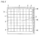
- the base substrate 1 is provided at the first surface side with an array (in this instance, two-dimensional array) of pixel parts 2 (see FIG. 3 ) each of which has a thermal-type infrared sensing part 3 and a MOS transistor 4 that is an pixel selecting switching element.
- the base substrate 1 is formed of a silicon substrate 1a.
- m x n in the example of FIGS. 3 and 13 , but not limited to, 8 x 8) pixel parts 2 are formed on the first surface side of one base substrate 1.
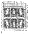
- a temperature sensor 30 of the thermal-type infrared sensing part 3 is formed of a plurality of (e.g., six) thermosensors 30a (see FIG. 1 ) each of which is formed of a thermopile and which are connected in series so that a sum of each absolute value output of the thermosensors 30a is obtained.
- an equivalent circuit of a temperature sensor 30 in the thermal-type infrared sensing part 3 is represented by a voltage source Vs corresponding to thermal electromotive force of the temperature sensor 30.
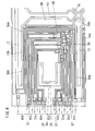
- the infrared array sensor A of the embodiment includes vertical read lines 7, horizontal signal lines 6, ground lines 8, a common ground line 9 and reference bias lines 5.
- Each of the vertical read lines 7 is commonly connected with first ends of a column of temperature sensors 30 in the thermal-type infrared sensing parts 3 through a column of MOS transistors 4.
- Each of the horizontal signal lines 6 is commonly connected with gate electrodes 46 of MOS transistors 4 corresponding to a row of temperature sensors 30 in the thermal-type infrared sensing parts 3.
- Each of the ground lines 8 is commonly connected with p + well regions 41 of a column of MOS transistors 4.
- the common ground line 9 is commonly connected with the ground lines 8.
- Each of the reference bias lines 5 is commonly connected with second ends of a column of temperature sensors 30 in the thermal-type infrared sensing parts 3.
- the sensor is adapted to provide, as time-series data, outputs of all the temperature sensors 30 in the thermal-type infrared sensing parts 3.
- the infrared array sensor A of the embodiment is formed with pixel parts 2 having, at the first surface side of the base substrate 1, thermal-type infrared sensing parts 3 and MOS transistors 4 which are laid side by side with the infrared sensing parts 3 and adapted to read out the outputs of the infrared sensing parts 3.
- the gate electrode 46 of a MOS transistor 4 is connected to a horizontal signal line 6, and its source electrode 48 is connected to a reference bias line 5 through a temperature sensor 30, and its drain electrode 47 is connected to a vertical read line 7.
- Each reference bias line 5 is commonly connected to a common reference bias line 5a.
- the horizontal signal lines 6 are electrically connected to discrete pixel selecting pads Vsel, respectively.
- the vertical read lines 7 are electrically connected to discrete output pads Vout, respectively.
- the common ground line 9 is electrically connected to a ground pad Gnd.
- the common reference bias line 5a is electrically connected to a reference bias pad Vref.
- the silicon substrate 1a is electrically connected to a substrate pad Vdd.
- each output voltage of the pixel parts 2 by controlling each electric potential of the pixel selecting pads Vsel so that the MOS transistors 4 are turned on sequentially.
- electric potential of the reference bias pad Vref electric potential of the ground pad Gnd and electric potential of the substrate pad Vdd are set to 1.65, 0V and 5V, respectively
- electric potential of a pixel selecting pad Vsel is set to 5V
- MOS transistors 4 are turned on and each output voltage of pixel parts 2 (1.65V + "output voltage of temperature sensor 30" is read out from the output pads Vout.
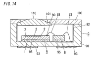
- an infrared array sensor module may include an infrared array sensor A, a signal processing IC chip B configured to perform the signal processing of output voltages as output signals of the infrared array sensor A, and a package C in which the infrared array sensor A and the signal processing IC chip B are put.
- a thermal imaging can be obtained if the signal processing IC chip B is provided with: pads (not shown) which are electrically connected to the pads 80 of the infrared array sensor A through wires 81 formed of bonding wires, respectively; an amplifier circuit configured to amplify each output voltage of pads (hereinafter referred to as "input pads") of the pads, connected to the output pads Vout of the infrared array sensor A; and a multiplexer configured to alternatively supply output voltages of the input pads to the amplifier circuit.
- the package C is composed of a package body 90 and a package lid 100.
- the package body 90 is formed of a multilayer ceramic substrate (a ceramic package) which is in the shape of a rectangular case having an opening at its one face, and the infrared array sensor A and the signal processing IC chip B are mounted on its inner bottom face.
- the package lid 100 is a metal lid which is attached to the one face side of the package body 90, and includes a lens 110 configured to focus infrared rays on the infrared array sensor A.
- a airtight space enclosed by the package body 90 and the package lid 100 is a dry nitrogen atmosphere.
- the periphery of the package lid 100 is fixed, by seam welding, to a rectangular frame shaped metal pattern (not shown) formed on the one face of the package body 90.
- the package body 90 is not limited to the multilayer ceramic substrate.
- the body may be formed of laminated glass epoxy resin substrates.
- a shield conductive pattern 92 is formed over the inner face of the package body 90.
- the infrared array sensor A and the signal processing IC chip are joined to the shield conductive pattern 92 of the package body 90 through joining layers 95, 95 formed of conductive junction material (e.g., solder, silver paste or the like).
- the joining method of the infrared array sensor A and the signal processing IC chip B to the package body 90 is not limited to the method using the conductive junction material such as solder or silver paste.
- a room-temperature bonding method a joining method using, e.g., Au-Sn eutectic or Au-Si eutectic may be employed.
- a joining method capable of direct joining such as a room-temperature bonding method is of advantage to improvement of distance accuracy between the infrared array sensor 5 and the lens 110 in comparison with a joining method using conductive junction material.
- the material of the lens 110 in the instance is Si as a kind of infrared-transparent material, and may be formed by a LIGA process, a method for manufacturing a semiconductor lens based on anodic oxidation technology (e.g., Japanese Patent Nos. 3897055 , 3897056 ), or the like.
- the lens 110 is adhered, by electrically conductive adhesive (e.g., solder, silver paste or the like), to the periphery of an open window 101 of the package lid 100 so that the open window 101 is shut.
- the lens 110 is also electrically connected to the shield conductive pattern 92 of the package body 90. Therefore, in the infrared array sensor module, it is possible to prevent the decrease of an S/N ratio caused by exogenous electromagnetic noise.
- the lens 110 may be provided with a necessary, appropriate infrared optical filter (a band-pass filter, a broadband cutoff filter, etc.) formed by alternately laminating films different in refractive index.
- the base substrate 1 of the infrared array sensor A has a peripheral shape of a rectangle. All of the pads 80 in the infrared array sensor A are arranged side by side along a side of peripheral edges of the base substrate 1.
- the signal processing IC chip B has a peripheral shape of a rectangle.
- the signal processing IC chip B is provided, along a side of its peripheral edges, with the aforementioned pads which are electrically connected to the pads 80 of the infrared array sensor A, respectively.
- the infrared array sensor A and the signal processing IC chip B are arranged so that the aforementioned their sides become nearer to each other than their other sides. Accordingly, it is possible to shorten the wires 81 connecting between the pads 80 of the infrared array sensor A and the pads of the signal processing IC chip B. Therefore, exogenous noise can be reduced and the noise resistance is improved.
- a single-crystal silicon substrate of which conduction type and first surface are n-type and (100) surface, respectively is employed as the silicon substrate 1a.
- a thermal-type infrared sensing part 3 is formed in the forming regions A1 of a thermal-type infrared sensing part 3.
- a MOS transistor 4 is formed in the forming region A2 of a MOS transistor 4.
- each pixel part 2 includes: an infrared absorption part 33 for absorbing infrared rays; a cavity 11 which is formed in the base substrate 1 and thermally insulates the infrared absorption part 33 from the base substrate 1; and a membrane structure (a thin film structure) 3a which covers the cavity 11 and has the infrared absorption part 33 within the cavity 11 in plane view from the first surface side of the base substrate 1.
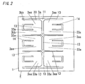
- Each membrane structure 3a in the pixel parts 2 is divided, by linear slits 13, into a plurality of (in the example of FIG.
- each of the segmented membrane structures 3aa is provided with a thermosensor 30a, and all of the thermosensors 30a are electrically connected at a relation of connection that an output change in response to temperature change becomes larger than that of the case where each output is separately obtained from each thermosensor 30a.
- Each pixel part 2 is formed with a coupling piece 3c for coupling adjoining segmented membrane structures 3aa, 3aa.
- each of parts, of each infrared absorption part 33, corresponding to segmented membrane structures 3aa, respectively is referred to as a segmented infrared absorption part 33a.
- thermosensors 30a formed on a membrane structure 3a in the example above, all of six thermosensors 30a may not always be connected in series.
- a series circuit of three thermosensors 30a and another series circuit of three thermosensors 30a may be connected in parallel.
- the sensitivity can be increased in comparison with the case that all of the six thermosensors 30a are connected in parallel or each output is separately obtained from each thermosensor 30a.
- the electric resistance of a temperature sensor 30 can be decreased and its thermal noise is decreased, and accordingly the S/N ratio is improved.
- each segmented membrane structure 3aa in a pixel part 2 is formed with two bridge parts 3bb, 3bb in the shape of a rectangle in plane view, which are formed and spaced in a circumferential direction of the cavity 11 and couple the base substrate 1 and the segmented infrared absorption part 33a.
- Each segmented membrane structure 3aa is formed with a slit 14 in the shape of a horseshoe in plane view, which spatially separates the two bridge parts 3bb, 3bb and the segmented infrared absorption part 33a and communicates with the cavity 11.
- a part of the base substrate 1, surrounding the membrane structure 3a in plane view is in the shape of a rectangular frame.
- a part, except for parts connected with the infrared absorption part 33 and the base substrate 1, of a bridge part 33b is spatially separated from the segmented infrared absorption part 33a and the base substrate 1 by slits 13 and 14.
- the dimension in an extended direction of a segmented membrane structure 3aa from the base substrate 1 is set to 93 ⁇ m
- the dimension in a width direction perpendicular to the extended direction of the segmented membrane structure 3aa is set to 75 ⁇ m
- a width dimension of each bridge part 33b is set to 23 ⁇ m
- each width of slits 13 and 14 is set to 5 ⁇ m.
- the membrane structure 3a is formed by patterning a laminated structure including: a silicon dioxide film 1b formed on the first surface side of the silicon substrate 1a; a silicon nitride film 32 formed on the silicon dioxide film 1b; a temperature sensor 30 formed on the silicon nitride film 32; an interlayer dielectric film 50 formed of a BPSG film covering the temperature sensor 30 at the surface side of the silicon nitride film 32; and a passivation film 60 formed of laminated films of a PSG film formed on the interlayer dielectric film 50 and an NSG film formed on the PSG film.
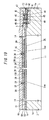
- the aforementioned infrared absorption part 33 is formed of a part of the silicon nitride film 32, except for the bridge parts 3bb, 3bb of the membrane structure 3a.
- the base substrate 1 is composed of the silicon substrate 1a, the silicon dioxide film 1b, the silicon nitride film 32, the interlayer dielectric film 50 and the passivation film 60.
- laminated films of the interlayer dielectric film 50 and the passivation film 60 are formed astride a forming region A1 of the thermal-type infrared sensing part 3 and a forming region A2 of the MOS transistor 4, and a part formed at the forming region A1 of the thermal-type infrared sensing part 3 also functions as the infrared absorbing film 70 (see FIG. 4B ).
- a refractive index of the infrared absorbing film 70 and a central wavelength of infrared rays from a detection object are n 2 and ⁇ , respectively, a thickness of the infrared absorbing film 70 (t2) is set to ⁇ /4n 2 .
- a thickness of the interlayer dielectric film 50 is 0.8 ⁇ m and a thickness of the passivation film 60 is 1 ⁇ m (a thickness of the PSG film is 0.5 ⁇ m and a thickness of the NSG film is 0.5 ⁇ m).
- the infrared absorbing film 70 is not limited to the aforementioned structure.
- the film may be formed of a silicon nitride film.
- Each thermosensor 30a in the pixel parts 2 is also a thermopile and the aforementioned relation of connection is a serial connection.
- each inner circumference of the cavities 11 is in the shape of a rectangle.
- Each coupling piece 3c is in the shape of a cross in plane view, and couples: segmented membrane structures 3aa, 3aa adjoined in a diagonal direction intersecting with an extension direction of the segmented membrane structures 3aa; segmented membrane structures 3aa, 3aa adjoined in an extension direction of the segmented membrane structures 3aa; and segmented membrane structures 3aa, 3aa adjoined in an orthogonal direction to an extension direction of the segmented membrane structures 3aa.
- thermosensor 30a formed of a thermopile has a plurality of (in the example of FIG. 1 , nine) thermocouples each of which electrically connects between a first end of n-type polysilicon layer 34 (one of first and second thermosensor halves) and a first end of p-type polysilicon layer 35 (the other of first and second thermosensor halves) by a connection part (hot junction) 36 formed of metal material (e.g., Al-Si, etc.) at the side of infrared entrance of the segmented infrared absorption part 33a, wherein the n-type polysilicon layer 34 and the p-type polysilicon layer 35 are formed on the silicon nitride film 32 and formed astride the segmented membrane structure 3aa and the base substrate 1.
- a connection part (hot junction) 36 formed of metal material (e.g., Al-Si, etc.)
- connection part 37 formed of metal material (e.g., Al-Si, etc.).
- thermosensor 30a the first ends of the n-type polysilicon layer 34 and the p-type polysilicon layer 35 and a connection part 36 constitute a hot junction at the side of a segmented infrared absorption part 33a, while the second ends of the n-type polysilicon layer 34 and the p-type polysilicon layer 35 and a connection part 37 constitute a cold junction at the side of the base substrate 1.
- each of the segmented membrane structure (3aa) includes a plurality of (first to ninth) thermosensors (30a) that constitute a combinational circuit and are electrically connected to each other so that a sum of each absolute value output of the thermosensors (30a) is obtained.
- the thermosensors thermoopiles
- the thermosensors constitute a series circuit and are connected in series to each other so that a sum of each absolute value output of the thermosensors (30a) is obtained.
- a plurality of (six) combinational circuits in a plurality of (six) membrane structures 3a are electrically connected to each other so that a sum of each absolute value output of the combinational circuits is obtained.
- the series circuits are connected in series to each other so that a sum of each absolute value output of the series circuits is obtained.
- the aforementioned cavity 11 is in the shape of a four-sided pyramid and has a depth deeper at its central part than its circumference in plane view. Accordingly, a planar layout of the thermosensors 30a in each pixel part 2 is designed so that the hot junctions are gathered at the central part of the membrane structure 3a. That is, in two segmented membrane structures 3aa at the middle of a vertical direction of FIG. 1 , the connection parts 36 are arranged side by side along an arrangement direction of three segmented membrane structures 3aa as shown in FIGS. 1 and 5 .
- connection parts 36 are arranged and gathered at a place near to the segmented membrane structures 3aa at the middle of the arrangement direction of three segmented membrane structures 3aa as shown in FIGS. 1 and 6 .
- connection parts 36 are arranged and gathered at a place near to the segmented membrane structures 3aa at the middle of the arrangement direction of three segmented membrane structures 3aa as shown in FIG. 1 .
- connection parts 36 of the segmented membrane structures 3aa at the upper and lower sides of the vertical direction of FIG. 1 is the same as that of the connection parts 36 of the segmented membrane structures 3aa at the middle.
- an infrared absorption layer 39 (see FIGS. 1 , 4 and 10 ) is formed at a region at the side of infrared entrance of the silicon nitride film 32 where no thermosensor 30a is formed.
- the infrared absorption layer is formed of an n-type polysilicon layer, and absorbs infrared rays and prevents warping of the segmented membrane structure 3aa.
- a coupling piece 3C coupling adjoining segmented membrane structures 3aa, 3aa is provided with a reinforced layer 39b (see FIG. 7 ) which is formed of an n-type polysilicon layer and reinforces the coupling piece 3C.
- the reinforced layer 39b and the infrared absorption layer 39 have a continuous integrated structure.
- the coupling piece 3C is reinforced by the reinforced layer 39b, and accordingly it is possible to prevent breakage caused by stress generated by impact or external temperature change in use, and also to decrease breakage in production to improve fabrication yield.
- a length dimension L1 and a width dimension L2 of the coupling piece 3c and a width dimension L3 of the reinforced layer 39b are set to, but are not limited to, for example, 24 ⁇ m and 5 ⁇ m and 1 ⁇ m, respectively.
- each reinforced layer 39b are formed of the silicon substrate 1a and an n-type polysilicon layer, respectively as the aforementioned embodiment, it is necessary to make the width dimension of the reinforced layer 39b smaller than that of the coupling piece 3c and to locate both side edges of the reinforced layer 39b within both side edges of the coupling piece 3c in plane view in order to prevent etching of the reinforced layer 39b while the cavity 11 is formed.
- chamfer parts 3d, 3d are formed between both side edges of the coupling piece 3c and a side edge of the segmented membrane structure 3aa, respectively.
- a chamfer part 3e is also formed between orthogonal side edges of the cross-shaped coupling piece 3c. Therefore, in the infrared array sensor A of the embodiment, it is possible to reduce stress concentration at a connecting region of a coupling piece 3c and a segmented membrane structure 3aa in comparison with the case that no chamfer parts are formed as shown in FIG. 12A . Thereby, it is possible to reduce remaining stress and breakage generated in production to improve fabrication yield.
- each chamfer part 3d, 3e is R-chamfering of 3 ⁇ m but is not limited to the R-chamfering.
- each of them may be C-chamfering.
- each pixel part 2 is provided with a fault diagnosis wiring 139 formed of an n-type polysilicon layer drawn astride the base substrate 1 and one bridge part 3bb and a segmented membrane structure 33a and another bridge part 3bb. All of the fault diagnosis wirings 139 are connected in series. Therefore, by energizing a series circuit of m x n fault diagnosis wirings 139, it is possible to detect the presence of breakage such as a broken bridge 3bb.
- the infrared absorption layer 39, the reinforced layer 39b and the fault diagnosis wirings 139 contain the same n-type impurities (e.g., phosphorus) as the n-type polysilicon layer 34 at the same impurity concentration (e.g., 10 18 -10 20 cm -3 ), and are formed at the same time as the n-type polysilicon layer 34. It just needs to employ, for example, boron as p-type impurities of the p-type polysilicon layer 35 and to set its impurity concentration in an appropriate range of, for example, 10 18 -10 20 cm -3 .
- n-type impurities e.g., phosphorus
- impurity concentration e.g. 10 18 -10 20 cm -3
- each impurity concentration of the n-type polysilicon layer 34 and the p-type polysilicon layer 35 is 10 18 -10 20 cm -3 , and each resistance value of the thermocouples can be reduced and the S/N ratio can be improved.
- the infrared absorption layer 39, the reinforced layer 39b and the fault diagnosis wirings 139 are doped with the same n-type impurities as the n-type polysilicon layer 34 at the same impurity concentration, but they are not limited to the impurities. For example, they may be doped with the same impurities as the p-type polysilicon layer 35 at the same impurity concentration.
- each impurity concentration of the n-type polysilicon layer34, the p-type polysilicon layer 35, the infrared absorption layer 39, the reinforced layer 39b and the fault diagnosis wirings 139 is 10 18 -10 20 cm -3 . Accordingly, it is possible to increase the reflection of infrared rays while increasing the absorbed fraction of infrared rays, and to increase an S/N ratio of each output of the temperature sensors 30. It is also possible to form the infrared absorption layer 39, the reinforced layer 39b and the fault diagnosis wirings 139 at the same process as the n-type polysilicon layer34, and accordingly the cost can be decreased.
- connection part 36 and the connection part 37 in the temperature sensor 30 are separated and insulated by the interlayer dielectric film 50 at the first surface side of the base substrate 1 (see FIGS. 8 and 9 ). That is, the hot junction 36 is electrically connected to each first end of the polysilicon layers 34, 35 through contact holes 50a 1 , 50a 2 formed in the interlayer dielectric film 50.
- the connection part 37 at the cold junction side is electrically connected to each second end of the polysilicon layers 34, 35 through contact holes 50a 3 , 50a 4 formed in the interlayer dielectric film 50.
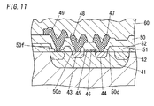
- a MOS transistor 4 is formed in a forming region A2 for MOS transistor 4 of each pixel part 2 in the first surface side of the silicon substrate 1a.
- a p + well region 41 is formed on the first surface side of the silicon substrate 1a, and an n + drain region 43 and an n + source region 44 are spaced and formed within the p + well region 41.
- a p ++ channel stopper region 42 surrounding the n + drain region 43 and the n + source region 44 is also formed within the p + well region 41.
- a gate electrode 46 of an n-type polysilicon layer is formed, through a gate insulating film 46 of a silicon dioxide film (thermally-oxidized film), on a part between the n + drain region 43 and the n + source region 44 within the p + well region 41.
- a drain electrode 47 is formed of metal material (e.g., Al-Si, etc.) and formed on the n + drain region 43.
- a source electrode 48 is formed of metal material (e.g., Al-Si, etc.) and formed on the n + source region 44. In this instance, the gate electrode 46, the drain electrode 47 and the source electrode 48 are separated and insulated by the interlayer dielectric film 50.
- the drain electrode 47 is electrically connected to the n + drain region 43 through a contact hole 50d formed in the interlayer dielectric film 50.
- the source electrode 48 is electrically connected to the n + source region 44 through the contact hole 50e formed in the interlayer dielectric film 50.
- thermosensor 30 is electrically connected to the source electrode 48 of a MOS transistor 4, and the second end of the thermosensor 30 is electrically connected to a reference bias line 5.
- drain electrode 47 of a MOS transistor 4 is electrically connected to a vertical read line 7, and its gate electrode 46 is electrically connected to a horizontal signal line 6 formed of an n-type polysilicon wire continuously integrated with the gate electrode 46.
- a ground electrode 49 formed of metal material is formed on the p ++ channel stopper region 42 of a MOS transistor 4, and the ground electrode 49 is electrically connected to a common ground line 8 for element isolation by biasing the p ++ channel stopper region 42 to make it lower potential than the n + drain region 43 and the n + source region 44.
- the ground electrode 49 is electrically connected to the p ++ channel stopper region 42 through a contact hole 50f formed in the interlayer dielectric film 50.
- an insulating layer forming process is performed, and an insulating layer is formed on the first surface side of a silicon substrate 1a, wherein the insulating layer is composed of laminated films of a first silicon dioxide film 31 having a first film thickness (e.g., 0.3 ⁇ m) and a silicon nitride film 32 having a second film thickness (e.g., 0.1 ⁇ m).
- An insulating layer patterning process is then performed by photolithography and etching technologies, and a part of the insulating layer, corresponding to a forming region A2 of a MOS transistor 4 is removed by etching so that a part corresponding to a forming region A1 of a thermal-type infrared sensing part 3 is remained.
- the silicon dioxide film 31 is formed by thermal oxidation of the silicon substrate 1a at a predetermined temperature (e.g., 1100°C), and the silicon nitride film 32 is formed by an LPCVD technique.
- a well region forming process is performed, and a p + well region 41 is formed on the first surface side of the silicon substrate 1a.
- a channel stopper region forming process is then performed, and a p ++ channel stopper region 42 is formed within the p + well region 41 at the first surface side of the silicon substrate 1.
- a second silicon dioxide film (thermally-oxidized film) 51 is selectively formed by thermal oxidation of an exposed area at the first surface side of the silicon substrate 1a at a predetermined temperature. Patterning of the silicon dioxide film 51 is then performed by using a mask for forming the p + well region 41 and photolithography and etching technologies.
- a third silicon dioxide film (thermally-oxidized film) 52 is selectively formed by thermal oxidation of the first surface side of the silicon substrate 1a at a predetermined temperature. Patterning of the third silicon dioxide film 52 is then performed by using a mask for forming the p ++ channel stopper region 42 and photolithography and etching technologies. Drive-in is then performed after ion implant of p-type impurities (e.g., boron, etc.), and thereby the p ++ channel stopper region 42 is formed.
- the first silicon dioxide film 31, the second silicon dioxide film 51 and the third silicon dioxide film 52 constitute a silicon dioxide film 1b on the first surface side of the silicon substrate 1a.
- a source and drain forming process is performed, and an n + drain region 43 and an n + source region 44 are formed by performing drive after ion implant of n-type impurities (e.g., phosphorus, etc.) into each forming region of the n + drain region 43 and the n + source region 44 in the p + well region 41.
- n-type impurities e.g., phosphorus, etc.
- a gate insulating film forming process is performed, and a gate insulating film 45 of a silicon dioxide film (thermally-oxidized film) having a given film thickness (e.g., 600 ⁇ ) is formed on the first surface side of the silicon substrate 1a by thermal oxidation.
- a polysilicon layer forming process is then performed, and a non-doped polysilicon layer having a given film thickness (e.g., 0.69 ⁇ m) is formed on the whole first surface side of the silicon substrate 1a by an LPCVD technique, wherein the non-doped polysilicon layer is the basis of gate electrodes 46, horizontal signal lines 6 (see FIG. 1 ), an n-type polysilicon layer 34, an p-type polysilicon layer 35, an infrared absorption layer 39, a reinforced layer 39b and fault diagnosis wirings 139.
- a given film thickness e.g. 0.69 ⁇ m
- a polysilicon layer patterning process is then performed by using photolithography and etching technologies, and the patterning is performed so that each part, of the non-doped polysilicon layer, corresponding to the gate electrodes 46, the horizontal signal lines 6, the n-type polysilicon layer 34, the p-type polysilicon layer 35, the infrared absorption layer 39, the reinforced layer 39b and the fault diagnosis wirings 139 is remained.
- a p-type polysilicon layer forming process is then performed, and a p-type polysilicon layer 35 is formed by performing drive after ion implant of p-type impurities (e.g., boron, etc.) into part corresponding to a p-type polysilicon layer 35 of the non-doped polysilicon layer.
- p-type impurities e.g., boron, etc.
- n-type polysilicon layer forming process is then performed, and the n-type polysilicon layer 34, the infrared absorption layer 39, the reinforced layer 39b, the fault diagnosis wirings 139, the gate electrodes 46 and the horizontal signal lines 6 are formed by performing drive after ion implant of n-type impurities (e.g., phosphorus, etc.) into each part, of the non-doped polysilicon layer, corresponding to the n-type polysilicon layer 34, the infrared absorption layer 39, the reinforced layer 39b, the fault diagnosis wiring 139, the gate electrodes 46 and the horizontal signal lines 6.
- n-type impurities e.g., phosphorus, etc.
- an interlayer dielectric film forming process is performed, and an interlayer dielectric film 50 is formed on the first surface side of the silicon substrate 1a.
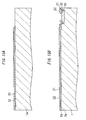
- a contact hole forming process is then performed by using photolithography and etching technologies, and contact holes 50a 1 , 50a 2 , 50a 3 , 50a 4 , 50d, 50e, 50f (see FIGS. 8 , 9 and 11 ) are in the interlayer dielectric film 50. Thereby, the structure shown in FIG. 16B is obtained.
- a BPSG film having a given film thickness (e.g., 0.8 ⁇ m) is deposited on the first surface side of the silicon substrate 1a by a CVD technique, and the interlayer dielectric film 50 is then formed by performing reflow at a predetermined temperature (e.g., 800°C).
- a metal film forming process is performed, and a metal film (e.g., Al-Si film, etc.) having a given film thickness (e.g., 2 ⁇ m) is formed on the whole first surface side of the silicon substrate 1a by a sputter technique, wherein the metal film is the basis of connection parts 36, 37, drain electrodes 47, source electrodes 48, reference bias lines 5, vertical read lines 7, ground lines 8, a common ground line 9, pads Vout, Vsel, Vref, Vdd, Gnd, and the like (see FIG. 13 ).
- a metal film e.g., Al-Si film, etc.
- a given film thickness e.g., 2 ⁇ m
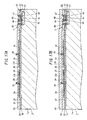
- a metal film patterning process for patterning the metal film is performed by photolithography and etching technologies, and connection parts 36, 37, drain electrodes 47, source electrodes 48, reference bias lines 5, vertical read lines 7, ground lines 8, a common ground line 9, pads Vout, Vsel, Vref, Vdd, Gnd, and the like are obtained. Thereby, the structure shown in FIG. 17A is obtained. In this instance, etching in the metal film patterning process is performed by RIE.
- a passivation film forming process is performed, and a passivation film 60 is formed on the first surface side of the silicon substrate 1a (i.e., on the surface side of the interlayer dielectric film 50) by a CVD technique, wherein the passivation film is formed of laminated films of a PSG film having a given film thickness (e.g., 0.5 ⁇ m) and an NSG film having a given film thickness (e.g., 0.5 ⁇ m).
- the passivation film 60 is not limited to the laminated films of the PSG film and the NSG film.
- the passivation film may be a silicon nitride film.
- a laminated structure patterning process is performed, and the segmented membrane structures 3aa are formed by patterning a laminated structure, wherein the laminated structure is composed of a thermal insulating layer formed of laminated films of the silicon dioxide film 31 and the silicon nitride film 32; the temperature sensors 30 formed on the thermal insulating layer; the interlayer dielectric film 50 covering the temperature sensors 30 from the surface side of the thermal insulating layer; and the passivation film 60 formed on the interlayer dielectric film 50.
- the laminated structure patterning process the aforementioned slits 13, 14 are formed.
- an opening forming process is formed by using photolithography and etching technologies, and openings (not shown) for exposing the pads Vout, Vsel, Vref, Vdd, Gnd are formed.
- a cavity forming process is then performed, and cavities 11 are formed in the silicon substrate 1a through anisotropic etching of the silicon substrate 1a by injecting etching solution through the slits 13, 14 as injection holes of etching solution.
- infrared array sensors A as shown in FIG. 18B are obtained, wherein each infrared array sensor A has a two-dimensional array of pixel parts 2.
- etching in the opening forming process is performed by RIE.
- TMAH solution heated at predetermined temperature e.g. 85°C
- the etching solution is not limited to the TMAH solution.
- the etching solution may be another alkaline solution (e.g., KOH solution, etc.). All processes are performed at wafer level until the cavity forming process is completed, and after the cavity forming process, a separation process for separating individual infrared array sensors A is performed.
- a commonly known method for producing MOS transistors is employed as a method for producing the MOS transistors 4, where p + well regions 41, p ++ channel stopper regions 42, n + drain regions 43 and n + source regions 44 are formed by repeating basic processes of: formation of a thermally-oxidized film by thermal oxidation; patterning of the thermally-oxidized film by photolithography and etching technologies; ion implantation of impurities; and drive-in (impurity diffusion).
- each pixel part 2 is formed with a cavity 11 in the base substrate 1 in order to thermally insulate an infrared absorption part 33 from the base substrate 1.
- a membrane structure 3a covering the cavity 11 is also formed, and has an infrared absorption part 33 within the cavity 11 in plane view at the first surface side of the base substrate 1.
- the membrane structure 3a is divided, by linear slits 13, into segmented membrane structures 3aa which are arranged along a circumferential direction of the cavity 11 and extended inwards from the periphery of the cavity 11 in the base substrate 1.
- Each segmented membrane structure 3aa is provided with a thermosensor 30a, and all of the thermosensors 30a are electrically connected at a relation of connection that output change in response to temperature change becomes large in comparison with the case that each output is separately obtained from each thermosensor 30a. Thereby, the response speed and sensitivity are improved. Moreover, coupling pieces 3c are formed and adjoining segmented membrane structures 3aa, 3aa are coupled, and thereby it is possible to reduce warping of each segmented membrane structure 3aa to improve the structural safety and stability of sensitivity.
- the sensor element (thermosensor) is formed of a resistive bolometer. Accordingly, there is a fear that the membrane structure warps by heat stress. Because, when detecting a change in resistance value, applying an electric current is required, which increases electric power consumption and produces self-heating.
- the resistor temperature coefficient also changes owing to a change in temperature by the self-heating or a change in ambient temperature, and accordingly it is difficult to attain high accuracy if a temperature compensation means is not provided. If the temperature compensation means is provided, the size and cost of the sensor are increased.
- thermosensors 30a of each pixel part 2 are thermopiles and the aforementioned relation of connection is a series connection. Therefore, in comparison with the case that each thermosensor 30a is formed of a resistive bolometer, there are advantages that prevents warping of each segmented membrane structure 3aa by self-heating, that decreases electric power consumption, and that provides high accuracy and a stable sensitivity regardless of temperature. Because applying an electric current to each thermosensor 30a is not required, and self-heating is not produced. When thermopiles are employed as the thermosensors 30a, if all of the thermosensors 30a are connected in series, each thermal electromotive force of the thermosensors 30a is added.
- thermosensor 30a just needs to be a thermal-type infrared sensing element, and is not limited to a thermopile or a resistive bolometer. Pyroelectric elements may be employed as the thermosensors. When each thermosensor 30a is a pyroelectric element, if pyroelectric elements are connected in parallel, each electric charge generated by a pyroelectric effect is added, and accordingly the aforementioned relation of connection can be satisfied and the sensitivity is increased.
- each cavity 11 is in the shape of a four-sided pyramid. Accordingly, when a silicon substrate is used as the base substrate 1, each cavity 11 can be easily formed though anisotropic etching by alkaline solution.
- the infrared absorption layer 39, the reinforced layer 39b and the fault diagnosis wirings 19 besides the n-type polysilicon layer 34 and the p-type polysilicon layer 35 are formed on the infrared entrance side of the silicon nitride film 32.
- the n-type polysilicon layer 34 and the p-type polysilicon layer 35 are formed, it is possible to prevent the silicon nitride film 32 from being thinned by etching (in this instance, to prevent the silicon nitride film 32 from being thinned by over-etching when the non-doped polysilicon layer is etched at the polysilicon layer patterning process, wherein the non-doped polysilicon layer is the basis of the n-type polysilicon layer 34 and the p-type polysilicon layer 35).
- the uniformity of stress balance of each membrane structure 3a can be increased.
- the n-type polysilicon layer 34, the p-type polysilicon layer 35, the infrared absorption layer 39, the reinforced layer 39b and the fault diagnosis wirings 19 are set to the same thickness. Accordingly, the uniformity of stress balance of each segmented membrane structure 3aa is improved, and it is possible to prevent warping of each segmented membrane structure 3aa.
- each pixel part 2 is provided with a MOS transistor 4 for reading out the output of the temperature sensor 30.
- the number of the output pads Vout can be reduced, and the size and cost can be decreased.
- the basic structure of an infrared array sensor A in the present embodiment is substantially the same as the embodiment 1, but differs in that each cavity 11 in a base substrate 1 is formed from the second surface side of the base substrate 1 as shown in FIG. 19 .
- Like kind elements are assigned the same reference numerals as depicted in the embodiment 1 and are not described in detail herein.
- each cavity 11 is formed through anisotropic etching of the silicon substrate 1a by utilizing crystal-face dependence of etching speed.
- an anisotropic etching technique using, for example, an ICP (Induction-Coupled Plasma) dry etching apparatus is used for each forming region of cavities 11 in a silicon substrate 1a from the second surface side of the base substrate 1.
- ICP Induction-Coupled Plasma
- the infrared array sensor of the embodiment it is possible to suppress heat transfer from each segmented membrane structure 3aa of a membrane structure 3a to the base substrate 1, and the sensitivity is more increased.
- the basic structure of an infrared array sensor A in the present embodiment is substantially the same as the embodiment 1, but differs in that each inner face of cavities 11 is a concave curve as shown in FIG. 20 .
- Like kind elements are assigned the same reference numerals as depicted in the embodiment 1 and are not described in detail herein.
- each cavity 11 is formed through anisotropic etching by utilizing crystal-face dependence of etching speed.
- each cavity 11 is formed through isotropic etching.
- infrared array sensor A of the embodiment it is possible to reflect infrared rays penetrating a membrane structure 3a into the membrane structure 3a by the inner face of a cavity 11. Absorbed amount of infrared rays at an infrared absorption part 33 can be increased and sensitivity is improved.
- the basic structure of an infrared array sensor A in the present embodiment is substantially the same as the embodiments 1-3, but differs in that an opening 12 communicating with cavities 11 is formed at the second surface side of a base substrate 1 as shown in FIG. 21 . That is, each of the cavities 11 includes an opening at the second surface side of the base substrate 1, and the base substrate 1 has, at he second surface side of the base substrate 1, one opening 12 including the cavities 11.
- Like kind elements are assigned the same reference numerals as depicted in the embodiments 1-3 and are not described in detail herein.
- the opening 12 of the base substrate 1 it just needs to utilize an anisotropic etching technique using, for example, an ICP dry etching apparatus for a forming region of the opening 12 in a silicon substrate 1a from the second surface side of the base substrate 1.
- the infrared array sensor A of the embodiment it is possible to more suppress heat transfer from each segmented membrane structure 3aa of a membrane structure 3a to the base substrate 1, and the sensitivity is more increased.
- the basic structure of an infrared array sensor A in the present embodiment is substantially the same as the embodiments 1-4, but differs in that as shown in FIG. 22 , segmented membrane structures 33a, 33a adjoined in an extended direction of segmented membrane structures 33a are coupled by coupling pieces 3c.
- segmented membrane structures 33a, 33a adjoined in an extended direction of segmented membrane structures 33a are coupled by coupling pieces 3c.
- Like kind elements are assigned the same reference numerals as depicted in the embodiments 1-4 and are not described in detail herein.
- segmented membrane structures 33a, 33a adjoined in the extended direction are coupled by two coupling pieces 3c which are spaced in a direction intersecting with the extended direction (i.e., in a width direction of each segmented membrane structure 3aa).
- segmented membrane structures 3aa, 3aa adjoined in an extended direction of the segmented membrane structures 3aa are coupled by coupling pieces 3c. Accordingly, first end sides of the segmented membrane structures 3aa, 3aa are directly supported by the periphery of a cavity 11 in a base substrate 1, while second end sides are supported by the periphery of the cavity 11 through the coupling pieces 3c and another segmented membrane structure 3aa. As a result, each segmented membrane structure 3aa is supported at both ends by the base substrate 1. Therefore, it is possible to reduce warping of each segmented membrane structure 3aa. The sensitivity is stabilized and fabrication yield is improved.
- segmented membrane structures 33a, 33a adjoined in the extended direction may be coupled by one coupling piece 3c at the middle of a width direction of each segmented membrane structure 3aa.
- the basic structure of an infrared array sensor A in the present embodiment is substantially the same as the embodiments 1-4, but differs in that as shown in FIG. 23 , adjoining segmented membrane structures 3aa, 3aa adjoined in a direction perpendicular to an extended direction of segmented membrane structures 3aa (in a width direction of each segmented membrane structure 3aa, namely in a vertical direction of FIG. 23 ) are coupled by a coupling piece 3c.
- Like kind elements are assigned the same reference numerals as depicted in the embodiments 1-4 and are not described in detail herein.
- segmented membrane structures 33a, 33a adjoined in the direction perpendicular to the extended direction are coupled by one coupling piece 3c at a part except for bridge parts 3bb. It is preferable that each coupling piece 3c is placed at a point distant from each bridge part 3bb.
- segmented membrane structures 3aa, 3aa adjoined in the direction perpendicular to the extended direction of the segmented membrane structures 3aa are coupled by a coupling piece 3c. Accordingly, torsional stiffness of each segmented membrane structure 3aa is increased, and deformation of each segmented membrane structure 3aa can be reduced. The sensitivity is stabilized and fabrication yield is improved.
- each pixel part 2 is a hexagonal shape in plane view and arranged in a honeycomb structure.
- Like kind elements are assigned the same reference numerals as depicted in the embodiments 1-6 and are not described in detail herein.
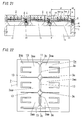
- a membrane structure 3a in the embodiment is divided, by six slits 13, into six segmented membrane structures 3aa which are coupled together by a coupling piece 3c.
- the infrared array sensor A of the embodiment can prevent deformation of each segmented membrane structure 3aa and increase configuration density of pixel parts 2.
- each pixel part 2 is provided with a MOS transistor 4, but need not necessarily include a MOS transistor 4.
Landscapes
- Physics & Mathematics (AREA)
- General Physics & Mathematics (AREA)
- Spectroscopy & Molecular Physics (AREA)
- Engineering & Computer Science (AREA)
- Chemical & Material Sciences (AREA)
- Nanotechnology (AREA)
- Manufacturing & Machinery (AREA)
- Multimedia (AREA)
- Signal Processing (AREA)
- Photometry And Measurement Of Optical Pulse Characteristics (AREA)
- Transforming Light Signals Into Electric Signals (AREA)
Abstract
Description
- The invention relates generally to infrared array sensors and, more particularly, to an infrared array sensor comprising a plurality of pixels.
- There is a conventional infrared array sensor researched and developed in various places, which are formed by using micromachining technologies and includes a base substrate and an array of pixel parts, having an infrared absorption part, located at one surface side of the base substrate (see Japanese Patent Application Publication No.
P2001-309122A - An infrared image sensor disclosed in the patent document includes a silicon substrate, and pixel forming regions are formed on a surface of the substrate. Sensor elements (e.g., bolometer sensor elements) are also placed on the pixel forming regions, respectively. The patent document also describes that each bolometer sensor element can be replaced with a pyroelectric sensor element or a thermopile sensor element.
- Specifically, each of the pixel forming regions is divided into four regions (hereinafter referred to as "segmented regions"), and four sensor elements are placed in the four segmented regions, respectively. Each of the four sensor elements is a membrane structure arranged so as to cover an opening of a depressed portion formed on a surface of the silicon substrate. The structure includes a SiO2 thin film, metallic thin film resistors (resistive bolometers) located on the thin film, a SiO2 thin film (second SiO2 thin film) located on the resistors, and an absorbing film located on the second SiO2 thin film.
- Thus, both ends of each sensor element formed in the four segmented regions are extended in a direction along a diagonal line of its own segmented region. The four sensor elements are connected in series by three conductive patterns on a surface of the silicon substrate (end face between depressed portions). Thereby, one pixel output is given by a sum of outputs of four sensor elements, and accordingly each pixel output can be increased. In comparison with a sensor of which each pixel forming region is provided with one sensor element, it is possible to reduce each heat capacity of the four segmented regions and a time constant (a thermal time constant). Therefore, the response speed can be increased.
- However, in the infrared image sensor, each of the pixel forming regions is divided into four segmented regions by a cross-shaped slit, and accordingly an area of a membrane structure per pixel is decreased by the slit. It is therefore difficult to increase the sensitivity of the sensor.
- If each thickness dimension of the membrane structures is increased, the sensitivity can be increased, but the response speed is reduced because each heat capacity of the membrane structures is increased. Conversely, if each thickness dimension of the membrane structures is decreased, the response speed is increased, but each membrane structure may warp in addition to an increase of the sensitivity, which thereby causes a decrease in yield by breakage in production. The decrease of structure stability may also cause reduction in sensitivity.
- Each of the sensor elements formed in the four segmented regions is supported by the silicon substrate through two linear arms extended in a direction along a diagonal line of its own segmented region. Accordingly, each membrane structure may be deformed by external force such as vibration or the like.
- It is an object of the present invention to improve the structure stability in addition to improvement of the response speed and sensitivity.
- An infrared array sensor of the present invention comprises: a base substrate (1) comprising first and second surfaces; cavities (11) which have array structure and are formed on the first surface side of the base substrate (1); and pixel parts (2) which are supported by the base substrate (1) to cover the cavities (11), respectively, each of the pixel parts comprising a membrane structure (3a). Each membrane structure (3a) of the pixel parts (2) comprises segmented membrane structures (3aa) divided by slits (13). Each of the segmented membrane structures (3aa) comprises a thermosensor (30a). Preferably, each membrane structure (3a) of the pixel parts (2) comprises a coupling piece (3c) for coupling its own segmented membrane structures (3aa) to each other.
- In this invention, structure stability can be improved and sensitivity stability can be enhanced.
- In an embodiment, each membrane structure (3a) of the pixel parts (2) comprises thermosensors (30a) that are electrically connected to each other so that a sum of each absolute value output of the thermosensors (30a) is obtained. In this embodiment, response speed and sensitivity can be improved.
- In an embodiment, each thermosensor (30a) of the pixel parts (2) is a thermopile. Thermosensors (30a) of each membrane structure (3a) of the pixel parts (2) are electrically connected in series to each other so that a sum of each absolute value output of the thermosensors (30a) is obtained. In this embodiment, it is unnecessary to apply an electric current to each thermosensor, and accordingly self-heating is not produced. Therefore, it is possible to prevent each segmented membrane structure (3aa) from warping owing to self-heating. The embodiment also has advantages such as electric power saving, and high-precision sensitivity free of the influence of temperature.
- In an embodiment, each of said segmented membrane structures (3aa) is supported by the base substrate (1) through a bridge part (3bb). Said bridge part (3bb) and the segmented membrane structure (3aa) supported by the base substrate (1) therethrough are in the shape of a rectangle surrounded by two or three slits (13). Said two or three slits are divided by one or two coupling pieces (3c).
- In an embodiment, each inner circumference of the cavities (11) is in the shape of a rectangle. Said segmented membrane structures (3aa) comprise two segmented membrane structures (3aa) arranged so as to approach to each other from both sides of an opening of a corresponding cavity (11). Said two segmented membrane structures (3aa) are coupled to each other by said one or two coupling pieces (3c). In this embodiment, it is possible to reduce warping of each of the two segmented membrane structures (3aa). The sensitivity is stabilized and fabrication yield is improved.
- In an embodiment, each inner circumference of the cavities (11) is in the shape of a rectangle. Said segmented membrane structures (3aa) comprise two segmented membrane structures (3aa) laying next to each other along one side of an opening of a corresponding cavity (11). Said two segmented membrane structures (3aa) are coupled to each other by said one coupling piece (3c). In this embodiment, each torsional stiffness of the two segmented membrane structures (3aa) is increased. Thereby, each torsional deformation of the two segmented membrane structures (3aa) can be reduced and the sensitivity is stabilized and fabrication yield is improved.
- In an embodiment, chamfer parts (3d) are formed between both side edges of said coupling piece (3c) and a side edge of the segmented membrane structure (3aa), respectively. In this embodiment, it is possible to absorb stress concentration at the coupling region of said coupling piece and said segmented membrane structure in comparison with the case that no chamfer parts are formed. The remaining stress and breakage generated in production can be reduced, and fabrication yield is improved. It is also possible to prevent breakage caused by stress generated by impact or external temperature change in use.
- In an embodiment, the coupling piece (3c) comprises a reinforced layer (39b) for reinforcing the coupling piece (3c). In this embodiment, it is also possible to prevent breakage caused by stress generated by impact or external temperature change in use. The breakage in production can be reduced, and fabrication yield is improved.
- In an embodiment, each of the cavities (11) is in the shape of a four-sided pyramid. In this embodiment, when a silicon substrate is used as the base substrate (1), each
cavity 11 can be easily formed by anisotropic etching using alkaline solution. - In an embodiment, each of the cavities (11) comprises an opening at the second surface side of the base substrate (1). In this embodiment, it is possible to suppress heat transfer from each membrane structure to the base substrate, and sensitivity is more increased.
- In an embodiment, the base substrate (1) comprises an opening (12) including the cavities (11) at the second surface side of the base substrate (1). In this embodiment, it is possible to more suppress heat transfer from each membrane structure to the base substrate, and sensitivity is more increased.
- In an embodiment, each inner face of the cavities (11) is a concave curve. In this embodiment, it is possible to reflect infrared rays penetrating a membrane structure into the membrane structure by the inner face of a cavity Absorbed amount of infrared rays can be increased and sensitivity is improved.
- An infrared array sensor of the present invention comprises: a base substrate (1); cavities (11) which have array structure and are formed on a surface side of the base substrate (1); and pixel parts (2) which are supported by the base substrate (1) to cover the cavities (11), respectively, each of the pixel parts comprising a membrane structure (3a). Each membrane structure (3a) of the pixel parts (2) comprises segmented membrane structures (3aa) divided by slits (13). Each of the segmented membrane structures (3aa) comprises thermosensors (30a). The thermosensors (30a) are electrically connected to each other so that a sum of each absolute value output of the thermosensors (30a) is obtained. Preferably, the thermosensors (30a) is a thermopile each, and are electrically connected in series to each other so that a sum of each absolute value output of the thermosensors (30a) is obtained. In this embodiment, the response speed and sensitivity can be further improved. The embodiment may comprise a coupling piece (3c).
- An infrared array sensor of the present invention comprises: a base substrate (1); cavities (11) which have array structure and are formed on a surface side of the base substrate (1); and pixel parts (2) which are supported by the base substrate (1) to cover the cavities (11), respectively, each of the pixel parts comprising a membrane structure (3a). Each membrane structure (3a) of the pixel parts (2) comprises segmented membrane structures (3aa) divided by slits (13). Each of the segmented membrane structures (3aa) comprises a thermosensor (30a). Each of said segmented membrane structures (3aa) is supported by the base substrate (1) through a bridge part (3bb). Said bridge part (3bb) and the segmented membrane structure (3aa) supported by the base substrate (1) therethrough comprises a thermosensor (30a) comprised of first and second thermosensor halves which are electrically connected to each other at a connecting point as a hot junction. The hot junction is placed in the segmented membrane structure (3aa), while both ends of the thermosensor (30a) is placed at the base substrate side. In addition, the hot junctions in the segmented membrane structures (3aa) are placed at the central part of the segmented membrane structures (3aa). In this embodiment, each temperature change in hot junctions can be increased, and accordingly the sensitivity can be improved. The embodiment may comprise a coupling piece (3c).
- Preferred embodiments of the invention will now be described in further details. Other features and advantages of the present invention will become better understood with regard to the following detailed description and accompanying drawings where:
-
FIG. 1 is a plane layout chart of a pixel part in an infrared array sensor of anembodiment 1; -
FIG. 2 is a plane layout chart of the pixel part in the infrared array sensor; -
FIG. 3 is a plane layout chart of the infrared array sensor; -
FIG. 4A and 4B show an essential part of the pixel part in the infrared array sensor, and are a plane layout chart and a schematic cross sectional view along line D-D' ofFIG. 4A , respectively; -
FIG. 5 is a plane layout chart of an essential part of the pixel part in the infrared array; -
FIG. 6 is a plane layout chart of an essential part of the pixel part in the infrared array; -
FIG. 7A and 7B show an essential part of the pixel part in the infrared array sensor, and are a plane layout chart and a schematic cross sectional view along line D-D' ofFIG. 7A , respectively; -
FIG. 8A and 8B show an essential part of the pixel part in the infrared array sensor, and are a plane layout chart and a schematic cross sectional view, respectively; -
FIG. 9A and 9B show an essential part of the pixel part in the infrared array sensor, and are a plane layout chart and a schematic cross sectional view, respectively; -
FIG. 10 is a schematic cross sectional view of an essential part of the pixel part in the infrared array sensor; -
FIG. 11 is a schematic cross sectional view of an essential part of the pixel part in the infrared array sensor; -
FIG. 12 is an explanatory diagram of an essential part of the infrared array sensor; -
FIG. 13 is an equivalent circuit schematic of the infrared array sensor; -
FIG. 14 is a schematic cross sectional view of an infrared module having the infrared array sensor; -
FIG. 15 is, as an explanatory diagram of a method for manufacturing the infrared array sensor, its cross sectional view in a principal process; -
FIG. 16 is a cross sectional view in a principal process, as an explanatory diagram, of a method for manufacturing the infrared array sensor; -
FIG. 17 is a cross sectional view in a principal process, as an explanatory diagram, of a method for manufacturing the infrared array sensor; -
FIG. 18 is a cross sectional view in a principal process, as an explanatory diagram, of a method for manufacturing the infrared array sensor; -
FIG. 19 is a schematic cross sectional view of a pixel part in an infrared array sensor of anembodiment 2; -
FIG. 20 is a schematic cross sectional view of a pixel part in an infrared array sensor of anembodiment 3; -
FIG. 21 is a schematic cross sectional view of a pixel part in an infrared array sensor of anembodiment 4; -
FIG. 22 is a plane layout chart of a pixel part in an infrared array sensor of anembodiment 5; -
FIG. 23 is a plane layout chart of a pixel part in an infrared array sensor of anembodiment 6; -
FIG. 24 is a plane layout chart of a pixel part in an infrared array sensor of anembodiment 7; and -
FIG. 25 is an enlarged view of an essential part in the plane layout chart of the pixel part. - An infrared array sensor A of the embodiment is explained with reference to
FIGS. 1-13 . - The infrared array sensor A of the embodiment includes a
base substrate 1 having a first surface (a front surface) and a second surface (a back surface). Thebase substrate 1 is provided at the first surface side with an array (in this instance, two-dimensional array) of pixel parts 2 (seeFIG. 3 ) each of which has a thermal-typeinfrared sensing part 3 and aMOS transistor 4 that is an pixel selecting switching element. Thebase substrate 1 is formed of asilicon substrate 1a. In the embodiment, m x n (in the example ofFIGS. 3 and13 , but not limited to, 8 x 8)pixel parts 2 are formed on the first surface side of onebase substrate 1. In the embodiment, atemperature sensor 30 of the thermal-typeinfrared sensing part 3 is formed of a plurality of (e.g., six) thermosensors 30a (seeFIG. 1 ) each of which is formed of a thermopile and which are connected in series so that a sum of each absolute value output of thethermosensors 30a is obtained. InFIG. 13 , an equivalent circuit of atemperature sensor 30 in the thermal-typeinfrared sensing part 3 is represented by a voltage source Vs corresponding to thermal electromotive force of thetemperature sensor 30. - As shown in
FIGS. 1 ,4 and13 , the infrared array sensor A of the embodiment includesvertical read lines 7,horizontal signal lines 6,ground lines 8, a common ground line 9 and reference bias lines 5. Each of thevertical read lines 7 is commonly connected with first ends of a column oftemperature sensors 30 in the thermal-typeinfrared sensing parts 3 through a column ofMOS transistors 4. Each of thehorizontal signal lines 6 is commonly connected withgate electrodes 46 ofMOS transistors 4 corresponding to a row oftemperature sensors 30 in the thermal-typeinfrared sensing parts 3. Each of theground lines 8 is commonly connected with p+ wellregions 41 of a column ofMOS transistors 4. The common ground line 9 is commonly connected with the ground lines 8. Each of thereference bias lines 5 is commonly connected with second ends of a column oftemperature sensors 30 in the thermal-typeinfrared sensing parts 3. The sensor is adapted to provide, as time-series data, outputs of all thetemperature sensors 30 in the thermal-typeinfrared sensing parts 3. In short, the infrared array sensor A of the embodiment is formed withpixel parts 2 having, at the first surface side of thebase substrate 1, thermal-typeinfrared sensing parts 3 andMOS transistors 4 which are laid side by side with theinfrared sensing parts 3 and adapted to read out the outputs of theinfrared sensing parts 3. - In this instance, the
gate electrode 46 of aMOS transistor 4 is connected to ahorizontal signal line 6, and itssource electrode 48 is connected to areference bias line 5 through atemperature sensor 30, and itsdrain electrode 47 is connected to avertical read line 7. Eachreference bias line 5 is commonly connected to a commonreference bias line 5a. Thehorizontal signal lines 6 are electrically connected to discrete pixel selecting pads Vsel, respectively. Thevertical read lines 7 are electrically connected to discrete output pads Vout, respectively. The common ground line 9 is electrically connected to a ground pad Gnd. The commonreference bias line 5a is electrically connected to a reference bias pad Vref. Thesilicon substrate 1a is electrically connected to a substrate pad Vdd. - Therefore, it is possible to sequentially read out each output voltage of the
pixel parts 2 by controlling each electric potential of the pixel selecting pads Vsel so that theMOS transistors 4 are turned on sequentially. For example, when electric potential of the reference bias pad Vref, electric potential of the ground pad Gnd and electric potential of the substrate pad Vdd are set to 1.65, 0V and 5V, respectively, if electric potential of a pixel selecting pad Vsel is set to 5V,MOS transistors 4 are turned on and each output voltage of pixel parts 2 (1.65V + "output voltage oftemperature sensor 30") is read out from the output pads Vout. If electric potential of a pixel selecting pad Vsel is set to 0V,MOS transistors 4 are turned off and no output voltage ofpixel parts 2 is read out from the output pads Vout. Incidentally, inFIG. 3 , all of the pixel selecting pads Vsel, the reference bias pad Vref, the ground pad Gnd, the output pads Vout and the like are depicted by 80 with no distinction. - As shown in
FIG. 14 , an infrared array sensor module may include an infrared array sensor A, a signal processing IC chip B configured to perform the signal processing of output voltages as output signals of the infrared array sensor A, and a package C in which the infrared array sensor A and the signal processing IC chip B are put. In this instance, a thermal imaging can be obtained if the signal processing IC chip B is provided with: pads (not shown) which are electrically connected to thepads 80 of the infrared array sensor A throughwires 81 formed of bonding wires, respectively; an amplifier circuit configured to amplify each output voltage of pads (hereinafter referred to as "input pads") of the pads, connected to the output pads Vout of the infrared array sensor A; and a multiplexer configured to alternatively supply output voltages of the input pads to the amplifier circuit. - The package C is composed of a
package body 90 and apackage lid 100. Thepackage body 90 is formed of a multilayer ceramic substrate (a ceramic package) which is in the shape of a rectangular case having an opening at its one face, and the infrared array sensor A and the signal processing IC chip B are mounted on its inner bottom face. Thepackage lid 100 is a metal lid which is attached to the one face side of thepackage body 90, and includes alens 110 configured to focus infrared rays on the infrared array sensor A. A airtight space enclosed by thepackage body 90 and thepackage lid 100 is a dry nitrogen atmosphere. In this example, the periphery of thepackage lid 100 is fixed, by seam welding, to a rectangular frame shaped metal pattern (not shown) formed on the one face of thepackage body 90. Thepackage body 90 is not limited to the multilayer ceramic substrate. For example, the body may be formed of laminated glass epoxy resin substrates. - In this instance, a shield
conductive pattern 92 is formed over the inner face of thepackage body 90. The infrared array sensor A and the signal processing IC chip are joined to the shieldconductive pattern 92 of thepackage body 90 through joininglayers package body 90 is not limited to the method using the conductive junction material such as solder or silver paste. For example, a room-temperature bonding method, a joining method using, e.g., Au-Sn eutectic or Au-Si eutectic may be employed. In this regard, a joining method capable of direct joining such as a room-temperature bonding method is of advantage to improvement of distance accuracy between theinfrared array sensor 5 and thelens 110 in comparison with a joining method using conductive junction material. - The material of the
lens 110 in the instance is Si as a kind of infrared-transparent material, and may be formed by a LIGA process, a method for manufacturing a semiconductor lens based on anodic oxidation technology (e.g., Japanese Patent Nos.3897055 3897056 lens 110 is adhered, by electrically conductive adhesive (e.g., solder, silver paste or the like), to the periphery of anopen window 101 of thepackage lid 100 so that theopen window 101 is shut. Thelens 110 is also electrically connected to the shieldconductive pattern 92 of thepackage body 90. Therefore, in the infrared array sensor module, it is possible to prevent the decrease of an S/N ratio caused by exogenous electromagnetic noise. Incidentally, thelens 110 may be provided with a necessary, appropriate infrared optical filter (a band-pass filter, a broadband cutoff filter, etc.) formed by alternately laminating films different in refractive index. - In the infrared array sensor module, the
base substrate 1 of the infrared array sensor A has a peripheral shape of a rectangle. All of thepads 80 in the infrared array sensor A are arranged side by side along a side of peripheral edges of thebase substrate 1. The signal processing IC chip B has a peripheral shape of a rectangle. The signal processing IC chip B is provided, along a side of its peripheral edges, with the aforementioned pads which are electrically connected to thepads 80 of the infrared array sensor A, respectively. The infrared array sensor A and the signal processing IC chip B are arranged so that the aforementioned their sides become nearer to each other than their other sides. Accordingly, it is possible to shorten thewires 81 connecting between thepads 80 of the infrared array sensor A and the pads of the signal processing IC chip B. Therefore, exogenous noise can be reduced and the noise resistance is improved. - Each configuration of the thermal-type
infrared sensing part 3 and theMOS transistor 4 is now explained. In the present embodiment, a single-crystal silicon substrate of which conduction type and first surface are n-type and (100) surface, respectively is employed as thesilicon substrate 1a. - In each
pixel part 2 on the first surface side of thesilicon substrate 1a, a thermal-typeinfrared sensing part 3 is formed in the forming regions A1 of a thermal-typeinfrared sensing part 3. In eachpixel part 2 on the first surface side of thesilicon substrate 1a, aMOS transistor 4 is formed in the forming region A2 of aMOS transistor 4. - By the way, each
pixel part 2 includes: aninfrared absorption part 33 for absorbing infrared rays; acavity 11 which is formed in thebase substrate 1 and thermally insulates theinfrared absorption part 33 from thebase substrate 1; and a membrane structure (a thin film structure) 3a which covers thecavity 11 and has theinfrared absorption part 33 within thecavity 11 in plane view from the first surface side of thebase substrate 1. Eachmembrane structure 3a in thepixel parts 2 is divided, bylinear slits 13, into a plurality of (in the example ofFIG. 1 , six) segmented membrane structures (small tin film structures) 3aa which are arranged side by side along a circumferential direction of the cavity and extended inwards from the periphery of thecavity 11 in thebase substrate 1. Each of the segmented membrane structures 3aa is provided with athermosensor 30a, and all of thethermosensors 30a are electrically connected at a relation of connection that an output change in response to temperature change becomes larger than that of the case where each output is separately obtained from eachthermosensor 30a. Eachpixel part 2 is formed with acoupling piece 3c for coupling adjoining segmented membrane structures 3aa, 3aa. Hereinafter, each of parts, of eachinfrared absorption part 33, corresponding to segmented membrane structures 3aa, respectively is referred to as a segmentedinfrared absorption part 33a. - Incidentally, all of
thermosensors 30a formed on amembrane structure 3a, in the example above, all of sixthermosensors 30a may not always be connected in series. For example, a series circuit of threethermosensors 30a and another series circuit of threethermosensors 30a may be connected in parallel. In this instance, the sensitivity can be increased in comparison with the case that all of the sixthermosensors 30a are connected in parallel or each output is separately obtained from eachthermosensor 30a. In addition, in comparison with the case that all of sixthermosensors 30a are connected in series, the electric resistance of atemperature sensor 30 can be decreased and its thermal noise is decreased, and accordingly the S/N ratio is improved. - In this instance, each segmented membrane structure 3aa in a
pixel part 2 is formed with two bridge parts 3bb, 3bb in the shape of a rectangle in plane view, which are formed and spaced in a circumferential direction of thecavity 11 and couple thebase substrate 1 and the segmentedinfrared absorption part 33a. Each segmented membrane structure 3aa is formed with aslit 14 in the shape of a horseshoe in plane view, which spatially separates the two bridge parts 3bb, 3bb and the segmentedinfrared absorption part 33a and communicates with thecavity 11. In this instance, a part of thebase substrate 1, surrounding themembrane structure 3a in plane view is in the shape of a rectangular frame. A part, except for parts connected with theinfrared absorption part 33 and thebase substrate 1, of a bridge part 33b is spatially separated from the segmentedinfrared absorption part 33a and thebase substrate 1 byslits base substrate 1 is set to 93µm, the dimension in a width direction perpendicular to the extended direction of the segmented membrane structure 3aa is set to 75µm, a width dimension of each bridge part 33b is set to 23µm, and each width ofslits - The
membrane structure 3a is formed by patterning a laminated structure including: asilicon dioxide film 1b formed on the first surface side of thesilicon substrate 1a; asilicon nitride film 32 formed on thesilicon dioxide film 1b; atemperature sensor 30 formed on thesilicon nitride film 32; aninterlayer dielectric film 50 formed of a BPSG film covering thetemperature sensor 30 at the surface side of thesilicon nitride film 32; and apassivation film 60 formed of laminated films of a PSG film formed on theinterlayer dielectric film 50 and an NSG film formed on the PSG film. - In the embodiment, the aforementioned
infrared absorption part 33 is formed of a part of thesilicon nitride film 32, except for the bridge parts 3bb, 3bb of themembrane structure 3a. Thebase substrate 1 is composed of thesilicon substrate 1a, thesilicon dioxide film 1b, thesilicon nitride film 32, theinterlayer dielectric film 50 and thepassivation film 60. In the embodiment, laminated films of theinterlayer dielectric film 50 and thepassivation film 60 are formed astride a forming region A1 of the thermal-typeinfrared sensing part 3 and a forming region A2 of theMOS transistor 4, and a part formed at the forming region A1 of the thermal-typeinfrared sensing part 3 also functions as the infrared absorbing film 70 (seeFIG. 4B ). In this instance, when a refractive index of the infrared absorbingfilm 70 and a central wavelength of infrared rays from a detection object are n2 and λ, respectively, a thickness of the infrared absorbing film 70 (t2) is set to λ/4n2. Accordingly, it is possible to increase absorption efficiency of infrared rays of a wavelength (e.g., 8-12µm) from the detection object, and the sensitivity is increased. For example, in the case of n2=1.4 and λ=10µm, it just needs to set t2≈1.8µm. Incidentally, in the embodiment, a thickness of theinterlayer dielectric film 50 is 0.8µm and a thickness of thepassivation film 60 is 1µm (a thickness of the PSG film is 0.5µm and a thickness of the NSG film is 0.5µm). The infrared absorbingfilm 70 is not limited to the aforementioned structure. For example, the film may be formed of a silicon nitride film. - Each
thermosensor 30a in thepixel parts 2 is also a thermopile and the aforementioned relation of connection is a serial connection. In eachpixel part 2, each inner circumference of thecavities 11 is in the shape of a rectangle. Eachcoupling piece 3c is in the shape of a cross in plane view, and couples: segmented membrane structures 3aa, 3aa adjoined in a diagonal direction intersecting with an extension direction of the segmented membrane structures 3aa; segmented membrane structures 3aa, 3aa adjoined in an extension direction of the segmented membrane structures 3aa; and segmented membrane structures 3aa, 3aa adjoined in an orthogonal direction to an extension direction of the segmented membrane structures 3aa. - A
thermosensor 30a formed of a thermopile has a plurality of (in the example ofFIG. 1 , nine) thermocouples each of which electrically connects between a first end of n-type polysilicon layer 34 (one of first and second thermosensor halves) and a first end of p-type polysilicon layer 35 (the other of first and second thermosensor halves) by a connection part (hot junction) 36 formed of metal material (e.g., Al-Si, etc.) at the side of infrared entrance of the segmentedinfrared absorption part 33a, wherein the n-type polysilicon layer 34 and the p-type polysilicon layer 35 are formed on thesilicon nitride film 32 and formed astride the segmented membrane structure 3aa and thebase substrate 1. Second ends (output terminals as cold junctions) of n-type polysilicon layer 34 and p-type polysilicon layer 35, as a thermocouple, adjoined at the first surface side of thebase substrate 1 are joined and electrically connected by aconnection part 37 formed of metal material (e.g., Al-Si, etc.). In the thermopile forming thethermosensor 30a in this instance, the first ends of the n-type polysilicon layer 34 and the p-type polysilicon layer 35 and aconnection part 36 constitute a hot junction at the side of a segmentedinfrared absorption part 33a, while the second ends of the n-type polysilicon layer 34 and the p-type polysilicon layer 35 and aconnection part 37 constitute a cold junction at the side of thebase substrate 1. - In short, as shown in
FIGS. 5 and6 , each of the segmented membrane structure (3aa) includes a plurality of (first to ninth) thermosensors (30a) that constitute a combinational circuit and are electrically connected to each other so that a sum of each absolute value output of the thermosensors (30a) is obtained. For example, the thermosensors (thermopiles) constitute a series circuit and are connected in series to each other so that a sum of each absolute value output of the thermosensors (30a) is obtained. In addition, a plurality of (six) combinational circuits in a plurality of (six)membrane structures 3a are electrically connected to each other so that a sum of each absolute value output of the combinational circuits is obtained. For example, the series circuits are connected in series to each other so that a sum of each absolute value output of the series circuits is obtained. - In the infrared array sensor A of the embodiment, the
aforementioned cavity 11 is in the shape of a four-sided pyramid and has a depth deeper at its central part than its circumference in plane view. Accordingly, a planar layout of thethermosensors 30a in eachpixel part 2 is designed so that the hot junctions are gathered at the central part of themembrane structure 3a. That is, in two segmented membrane structures 3aa at the middle of a vertical direction ofFIG. 1 , theconnection parts 36 are arranged side by side along an arrangement direction of three segmented membrane structures 3aa as shown inFIGS. 1 and5 . In two segmented membrane structures 3aa at the upper side of the vertical direction, theconnection parts 36 are arranged and gathered at a place near to the segmented membrane structures 3aa at the middle of the arrangement direction of three segmented membrane structures 3aa as shown inFIGS. 1 and6 . In two segmented membrane structures 3aa at the lower side of the vertical direction, theconnection parts 36 are arranged and gathered at a place near to the segmented membrane structures 3aa at the middle of the arrangement direction of three segmented membrane structures 3aa as shown inFIG. 1 . Therefore, in the infrared array sensor A of the embodiment, it is possible to increase temperature change in each hot junction to improve sensitivity in comparison with the case that the arrangement of theconnection parts 36 of the segmented membrane structures 3aa at the upper and lower sides of the vertical direction ofFIG. 1 is the same as that of theconnection parts 36 of the segmented membrane structures 3aa at the middle. - In a segmented membrane structure 3aa, an infrared absorption layer 39 (see
FIGS. 1 ,4 and10 ) is formed at a region at the side of infrared entrance of thesilicon nitride film 32 where nothermosensor 30a is formed. The infrared absorption layer is formed of an n-type polysilicon layer, and absorbs infrared rays and prevents warping of the segmented membrane structure 3aa. A coupling piece 3C coupling adjoining segmented membrane structures 3aa, 3aa is provided with a reinforcedlayer 39b (seeFIG. 7 ) which is formed of an n-type polysilicon layer and reinforces the coupling piece 3C. In this instance, the reinforcedlayer 39b and theinfrared absorption layer 39 have a continuous integrated structure. Thus, in the infrared array sensor A of the embodiment, the coupling piece 3C is reinforced by the reinforcedlayer 39b, and accordingly it is possible to prevent breakage caused by stress generated by impact or external temperature change in use, and also to decrease breakage in production to improve fabrication yield. In the embodiment, as shown inFIG. 7 , a length dimension L1 and a width dimension L2 of thecoupling piece 3c and a width dimension L3 of the reinforcedlayer 39b are set to, but are not limited to, for example, 24µm and 5µm and 1µm, respectively. When thebase substrate 1 and each reinforcedlayer 39b are formed of thesilicon substrate 1a and an n-type polysilicon layer, respectively as the aforementioned embodiment, it is necessary to make the width dimension of the reinforcedlayer 39b smaller than that of thecoupling piece 3c and to locate both side edges of the reinforcedlayer 39b within both side edges of thecoupling piece 3c in plane view in order to prevent etching of the reinforcedlayer 39b while thecavity 11 is formed. - In the infrared array sensor A of the embodiment, as shown in
FIGS. 7 and12B ,chamfer parts coupling piece 3c and a side edge of the segmented membrane structure 3aa, respectively. Achamfer part 3e is also formed between orthogonal side edges of thecross-shaped coupling piece 3c. Therefore, in the infrared array sensor A of the embodiment, it is possible to reduce stress concentration at a connecting region of acoupling piece 3c and a segmented membrane structure 3aa in comparison with the case that no chamfer parts are formed as shown inFIG. 12A . Thereby, it is possible to reduce remaining stress and breakage generated in production to improve fabrication yield. It is also possible to prevent breakage caused by stress generated by impact or external temperature change in use. In the example shown inFIG. 7 , eachchamfer part - In the infrared array sensor A of the embodiment, each
pixel part 2 is provided with afault diagnosis wiring 139 formed of an n-type polysilicon layer drawn astride thebase substrate 1 and one bridge part 3bb and asegmented membrane structure 33a and another bridge part 3bb. All of thefault diagnosis wirings 139 are connected in series. Therefore, by energizing a series circuit of m x n fault diagnosis wirings 139, it is possible to detect the presence of breakage such as a broken bridge 3bb. - The
infrared absorption layer 39, the reinforcedlayer 39b and thefault diagnosis wirings 139 contain the same n-type impurities (e.g., phosphorus) as the n-type polysilicon layer 34 at the same impurity concentration (e.g., 1018-1020cm-3), and are formed at the same time as the n-type polysilicon layer 34. It just needs to employ, for example, boron as p-type impurities of the p-type polysilicon layer 35 and to set its impurity concentration in an appropriate range of, for example, 1018-1020cm-3. In the embodiment, each impurity concentration of the n-type polysilicon layer 34 and the p-type polysilicon layer 35 is 1018-1020cm-3, and each resistance value of the thermocouples can be reduced and the S/N ratio can be improved. In this instance, theinfrared absorption layer 39, the reinforcedlayer 39b and thefault diagnosis wirings 139 are doped with the same n-type impurities as the n-type polysilicon layer 34 at the same impurity concentration, but they are not limited to the impurities. For example, they may be doped with the same impurities as the p-type polysilicon layer 35 at the same impurity concentration. - In the embodiment, each thickness t1 of the n-type polysilicon layer34, the p-
type polysilicon layer 35, theinfrared absorption layer 39, the reinforcedlayer 39b and the fault diagnosis wirings 139 is set to λ/4n1, where each refractive index of the n-type polysilicon layer34, the p-type polysilicon layer 35, theinfrared absorption layer 39, the reinforcedlayer 39b and the fault diagnosis wirings 139 is n1, and a central wavelength of infrared rays from a detection object is λ. Accordingly, an absorption efficiency of infrared rays of a wavelength (e.g., 8-12µm) from the detection object can be increased, and the sensitivity can be increased. For example, in the case of n1=3.6, λ=10µm, it just needs to set t1≈0.69µm. - In the embodiment, each impurity concentration of the n-type polysilicon layer34, the p-
type polysilicon layer 35, theinfrared absorption layer 39, the reinforcedlayer 39b and the fault diagnosis wirings 139 is 1018-1020cm-3. Accordingly, it is possible to increase the reflection of infrared rays while increasing the absorbed fraction of infrared rays, and to increase an S/N ratio of each output of thetemperature sensors 30. It is also possible to form theinfrared absorption layer 39, the reinforcedlayer 39b and thefault diagnosis wirings 139 at the same process as the n-type polysilicon layer34, and accordingly the cost can be decreased. - In this instance, the
connection part 36 and theconnection part 37 in thetemperature sensor 30 are separated and insulated by theinterlayer dielectric film 50 at the first surface side of the base substrate 1 (seeFIGS. 8 and9 ). That is, thehot junction 36 is electrically connected to each first end of the polysilicon layers 34, 35 through contact holes 50a1, 50a2 formed in theinterlayer dielectric film 50. Theconnection part 37 at the cold junction side is electrically connected to each second end of the polysilicon layers 34, 35 through contact holes 50a3, 50a4 formed in theinterlayer dielectric film 50. - A
MOS transistor 4 is formed in a forming region A2 forMOS transistor 4 of eachpixel part 2 in the first surface side of thesilicon substrate 1a. As shown inFIGS. 4 and11 , in theMOS transistor 4, a p+ well region 41 is formed on the first surface side of thesilicon substrate 1a, and an n+ drain region 43 and an n+ source region 44 are spaced and formed within the p+ well region 41. A p++channel stopper region 42 surrounding the n+ drain region 43 and the n+ source region 44 is also formed within the p+ well region 41. Agate electrode 46 of an n-type polysilicon layer is formed, through agate insulating film 46 of a silicon dioxide film (thermally-oxidized film), on a part between the n+ drain region 43 and the n+ source region 44 within the p+ well region 41. Adrain electrode 47 is formed of metal material (e.g., Al-Si, etc.) and formed on the n+ drain region 43. Asource electrode 48 is formed of metal material (e.g., Al-Si, etc.) and formed on the n+ source region 44. In this instance, thegate electrode 46, thedrain electrode 47 and thesource electrode 48 are separated and insulated by theinterlayer dielectric film 50. That is, thedrain electrode 47 is electrically connected to the n+ drain region 43 through acontact hole 50d formed in theinterlayer dielectric film 50. Thesource electrode 48 is electrically connected to the n+ source region 44 through thecontact hole 50e formed in theinterlayer dielectric film 50. - By the way, in each
pixel part 2 of the infrared array sensor A in the embodiment, the first end of athermosensor 30 is electrically connected to thesource electrode 48 of aMOS transistor 4, and the second end of thethermosensor 30 is electrically connected to areference bias line 5. Also, in eachpixel part 2 of the infrared array sensor A in the embodiment, thedrain electrode 47 of aMOS transistor 4 is electrically connected to avertical read line 7, and itsgate electrode 46 is electrically connected to ahorizontal signal line 6 formed of an n-type polysilicon wire continuously integrated with thegate electrode 46. Also, in eachpixel part 2, aground electrode 49 formed of metal material (e.g., Al-Si, etc.) is formed on the p++channel stopper region 42 of aMOS transistor 4, and theground electrode 49 is electrically connected to acommon ground line 8 for element isolation by biasing the p++channel stopper region 42 to make it lower potential than the n+ drain region 43 and the n+ source region 44. Theground electrode 49 is electrically connected to the p++channel stopper region 42 through acontact hole 50f formed in theinterlayer dielectric film 50. - A method for manufacturing the infrared array sensor A of the embodiment is now explained with reference to
FIGS. 15-18 . - First, an insulating layer forming process is performed, and an insulating layer is formed on the first surface side of a
silicon substrate 1a, wherein the insulating layer is composed of laminated films of a firstsilicon dioxide film 31 having a first film thickness (e.g., 0.3µm) and asilicon nitride film 32 having a second film thickness (e.g., 0.1µm). An insulating layer patterning process is then performed by photolithography and etching technologies, and a part of the insulating layer, corresponding to a forming region A2 of aMOS transistor 4 is removed by etching so that a part corresponding to a forming region A1 of a thermal-typeinfrared sensing part 3 is remained. Thereby, the structure shown inFIG. 15A is obtained. In this instance, thesilicon dioxide film 31 is formed by thermal oxidation of thesilicon substrate 1a at a predetermined temperature (e.g., 1100°C), and thesilicon nitride film 32 is formed by an LPCVD technique. - After the insulating layer patterning process, a well region forming process is performed, and a p+ well region 41 is formed on the first surface side of the
silicon substrate 1a. A channel stopper region forming process is then performed, and a p++channel stopper region 42 is formed within the p+ well region 41 at the first surface side of thesilicon substrate 1. Thereby, the structure shown inFIG. 15B is obtained. At the well region forming process, a second silicon dioxide film (thermally-oxidized film) 51 is selectively formed by thermal oxidation of an exposed area at the first surface side of thesilicon substrate 1a at a predetermined temperature. Patterning of thesilicon dioxide film 51 is then performed by using a mask for forming the p+ well region 41 and photolithography and etching technologies. Drive-in is then performed after ion implant of p-type impurities (e.g., boron, etc.), and thereby the p+ well region 41 is formed. At the channel stopper region forming process, a third silicon dioxide film (thermally-oxidized film) 52 is selectively formed by thermal oxidation of the first surface side of thesilicon substrate 1a at a predetermined temperature. Patterning of the thirdsilicon dioxide film 52 is then performed by using a mask for forming the p++channel stopper region 42 and photolithography and etching technologies. Drive-in is then performed after ion implant of p-type impurities (e.g., boron, etc.), and thereby the p++channel stopper region 42 is formed. Incidentally, the firstsilicon dioxide film 31, the secondsilicon dioxide film 51 and the thirdsilicon dioxide film 52 constitute asilicon dioxide film 1b on the first surface side of thesilicon substrate 1a. - After the channel stopper region forming process, a source and drain forming process is performed, and an n+ drain region 43 and an n+ source region 44 are formed by performing drive after ion implant of n-type impurities (e.g., phosphorus, etc.) into each forming region of the n+ drain region 43 and the n+ source region 44 in the p+ well region 41. After the source and drain forming process, a gate insulating film forming process is performed, and a
gate insulating film 45 of a silicon dioxide film (thermally-oxidized film) having a given film thickness (e.g., 600Å) is formed on the first surface side of thesilicon substrate 1a by thermal oxidation. A polysilicon layer forming process is then performed, and a non-doped polysilicon layer having a given film thickness (e.g., 0.69µm) is formed on the whole first surface side of thesilicon substrate 1a by an LPCVD technique, wherein the non-doped polysilicon layer is the basis ofgate electrodes 46, horizontal signal lines 6 (seeFIG. 1 ), an n-type polysilicon layer 34, an p-type polysilicon layer 35, aninfrared absorption layer 39, a reinforcedlayer 39b andfault diagnosis wirings 139. A polysilicon layer patterning process is then performed by using photolithography and etching technologies, and the patterning is performed so that each part, of the non-doped polysilicon layer, corresponding to thegate electrodes 46, thehorizontal signal lines 6, the n-type polysilicon layer 34, the p-type polysilicon layer 35, theinfrared absorption layer 39, the reinforcedlayer 39b and the fault diagnosis wirings 139 is remained. A p-type polysilicon layer forming process is then performed, and a p-type polysilicon layer 35 is formed by performing drive after ion implant of p-type impurities (e.g., boron, etc.) into part corresponding to a p-type polysilicon layer 35 of the non-doped polysilicon layer. An n-type polysilicon layer forming process is then performed, and the n-type polysilicon layer 34, theinfrared absorption layer 39, the reinforcedlayer 39b, the fault diagnosis wirings 139, thegate electrodes 46 and thehorizontal signal lines 6 are formed by performing drive after ion implant of n-type impurities (e.g., phosphorus, etc.) into each part, of the non-doped polysilicon layer, corresponding to the n-type polysilicon layer 34, theinfrared absorption layer 39, the reinforcedlayer 39b, thefault diagnosis wiring 139, thegate electrodes 46 and the horizontal signal lines 6. Thereby, the structure shown inFIG. 16A is obtained. The p-type polysilicon layer forming process and the n-type polysilicon layer forming process may be reverse order. - After completion of the p-type and n-type polysilicon layer forming processes, an interlayer dielectric film forming process is performed, and an
interlayer dielectric film 50 is formed on the first surface side of thesilicon substrate 1a. A contact hole forming process is then performed by using photolithography and etching technologies, andcontact holes FIGS. 8 ,9 and11 ) are in theinterlayer dielectric film 50. Thereby, the structure shown inFIG. 16B is obtained. In the interlayer dielectric film forming process, a BPSG film having a given film thickness (e.g., 0.8µm) is deposited on the first surface side of thesilicon substrate 1a by a CVD technique, and theinterlayer dielectric film 50 is then formed by performing reflow at a predetermined temperature (e.g., 800°C). - After the contact hole forming process, a metal film forming process is performed, and a metal film (e.g., Al-Si film, etc.) having a given film thickness (e.g., 2µm) is formed on the whole first surface side of the
silicon substrate 1a by a sputter technique, wherein the metal film is the basis ofconnection parts drain electrodes 47,source electrodes 48,reference bias lines 5,vertical read lines 7,ground lines 8, a common ground line 9, pads Vout, Vsel, Vref, Vdd, Gnd, and the like (seeFIG. 13 ). A metal film patterning process for patterning the metal film is performed by photolithography and etching technologies, andconnection parts drain electrodes 47,source electrodes 48,reference bias lines 5,vertical read lines 7,ground lines 8, a common ground line 9, pads Vout, Vsel, Vref, Vdd, Gnd, and the like are obtained. Thereby, the structure shown inFIG. 17A is obtained. In this instance, etching in the metal film patterning process is performed by RIE. - After the metal film patterning process, a passivation film forming process is performed, and a
passivation film 60 is formed on the first surface side of thesilicon substrate 1a (i.e., on the surface side of the interlayer dielectric film 50) by a CVD technique, wherein the passivation film is formed of laminated films of a PSG film having a given film thickness (e.g., 0.5µm) and an NSG film having a given film thickness (e.g., 0.5µm). Thereby, the structure shown inFIG. 17B is obtained. However, thepassivation film 60 is not limited to the laminated films of the PSG film and the NSG film. For example, the passivation film may be a silicon nitride film. - After the passivation film forming process, a laminated structure patterning process is performed, and the segmented membrane structures 3aa are formed by patterning a laminated structure, wherein the laminated structure is composed of a thermal insulating layer formed of laminated films of the
silicon dioxide film 31 and thesilicon nitride film 32; thetemperature sensors 30 formed on the thermal insulating layer; theinterlayer dielectric film 50 covering thetemperature sensors 30 from the surface side of the thermal insulating layer; and thepassivation film 60 formed on theinterlayer dielectric film 50. Thereby, the structure shown inFIG. 18A is obtained. In the laminated structure patterning process, theaforementioned slits - After the laminated structure patterning process, an opening forming process is formed by using photolithography and etching technologies, and openings (not shown) for exposing the pads Vout, Vsel, Vref, Vdd, Gnd are formed. A cavity forming process is then performed, and
cavities 11 are formed in thesilicon substrate 1a through anisotropic etching of thesilicon substrate 1a by injecting etching solution through theslits FIG. 18B are obtained, wherein each infrared array sensor A has a two-dimensional array ofpixel parts 2. In this instance, etching in the opening forming process is performed by RIE. In the cavity forming process, TMAH solution heated at predetermined temperature (e.g., 85°C) is employed as etching solution, but the etching solution is not limited to the TMAH solution. The etching solution may be another alkaline solution (e.g., KOH solution, etc.). All processes are performed at wafer level until the cavity forming process is completed, and after the cavity forming process, a separation process for separating individual infrared array sensors A is performed. As can be seen from the above explanation, a commonly known method for producing MOS transistors is employed as a method for producing theMOS transistors 4, where p+ wellregions 41, p++channel stopper regions 42, n+ drain regions 43 and n+ source regions 44 are formed by repeating basic processes of: formation of a thermally-oxidized film by thermal oxidation; patterning of the thermally-oxidized film by photolithography and etching technologies; ion implantation of impurities; and drive-in (impurity diffusion). - In the infrared array sensor A of the embodiment, each
pixel part 2 is formed with acavity 11 in thebase substrate 1 in order to thermally insulate aninfrared absorption part 33 from thebase substrate 1. Amembrane structure 3a covering thecavity 11 is also formed, and has aninfrared absorption part 33 within thecavity 11 in plane view at the first surface side of thebase substrate 1. Themembrane structure 3a is divided, bylinear slits 13, into segmented membrane structures 3aa which are arranged along a circumferential direction of thecavity 11 and extended inwards from the periphery of thecavity 11 in thebase substrate 1. Each segmented membrane structure 3aa is provided with athermosensor 30a, and all of thethermosensors 30a are electrically connected at a relation of connection that output change in response to temperature change becomes large in comparison with the case that each output is separately obtained from eachthermosensor 30a. Thereby, the response speed and sensitivity are improved. Moreover,coupling pieces 3c are formed and adjoining segmented membrane structures 3aa, 3aa are coupled, and thereby it is possible to reduce warping of each segmented membrane structure 3aa to improve the structural safety and stability of sensitivity. - Incidentally, in the infrared image sensor of the aforementioned patent document, the sensor element (thermosensor) is formed of a resistive bolometer. Accordingly, there is a fear that the membrane structure warps by heat stress. Because, when detecting a change in resistance value, applying an electric current is required, which increases electric power consumption and produces self-heating. The resistor temperature coefficient also changes owing to a change in temperature by the self-heating or a change in ambient temperature, and accordingly it is difficult to attain high accuracy if a temperature compensation means is not provided. If the temperature compensation means is provided, the size and cost of the sensor are increased.
- In the infrared array sensor A of the embodiment,
thermosensors 30a of eachpixel part 2 are thermopiles and the aforementioned relation of connection is a series connection. Therefore, in comparison with the case that eachthermosensor 30a is formed of a resistive bolometer, there are advantages that prevents warping of each segmented membrane structure 3aa by self-heating, that decreases electric power consumption, and that provides high accuracy and a stable sensitivity regardless of temperature. Because applying an electric current to eachthermosensor 30a is not required, and self-heating is not produced. When thermopiles are employed as thethermosensors 30a, if all of thethermosensors 30a are connected in series, each thermal electromotive force of thethermosensors 30a is added. Accordingly, the aforementioned relation of connection can be satisfied and the sensitivity is increased. Eachthermosensor 30a just needs to be a thermal-type infrared sensing element, and is not limited to a thermopile or a resistive bolometer. Pyroelectric elements may be employed as the thermosensors. When each thermosensor 30a is a pyroelectric element, if pyroelectric elements are connected in parallel, each electric charge generated by a pyroelectric effect is added, and accordingly the aforementioned relation of connection can be satisfied and the sensitivity is increased. - In the infrared array sensor A of the embodiment, each
cavity 11 is in the shape of a four-sided pyramid. Accordingly, when a silicon substrate is used as thebase substrate 1, eachcavity 11 can be easily formed though anisotropic etching by alkaline solution. - In the infrared array sensor A of the embodiment, the
infrared absorption layer 39, the reinforcedlayer 39b and the fault diagnosis wirings 19 besides the n-type polysilicon layer 34 and the p-type polysilicon layer 35 are formed on the infrared entrance side of thesilicon nitride film 32. Accordingly, when the n-type polysilicon layer 34 and the p-type polysilicon layer 35 are formed, it is possible to prevent thesilicon nitride film 32 from being thinned by etching (in this instance, to prevent thesilicon nitride film 32 from being thinned by over-etching when the non-doped polysilicon layer is etched at the polysilicon layer patterning process, wherein the non-doped polysilicon layer is the basis of the n-type polysilicon layer 34 and the p-type polysilicon layer 35). The uniformity of stress balance of eachmembrane structure 3a can be increased. It is also possible to prevent warping of each segmented membrane structure 3aa while thinning eachinfrared absorption part 33, and the sensitivity is improved. In this instance, it is necessary to design a shape in plane view so that the n-type polysilicon layer 34, the p-type polysilicon layer 35, theinfrared absorption layer 39, the reinforcedlayer 39b and the fault diagnosis wirings 19 do not expose in inner side surfaces of theslits - In the infrared array sensor A of the embodiment, the n-
type polysilicon layer 34, the p-type polysilicon layer 35, theinfrared absorption layer 39, the reinforcedlayer 39b and the fault diagnosis wirings 19 are set to the same thickness. Accordingly, the uniformity of stress balance of each segmented membrane structure 3aa is improved, and it is possible to prevent warping of each segmented membrane structure 3aa. - In the infrared array sensor A of the embodiment, each
pixel part 2 is provided with aMOS transistor 4 for reading out the output of thetemperature sensor 30. The number of the output pads Vout can be reduced, and the size and cost can be decreased. - The basic structure of an infrared array sensor A in the present embodiment is substantially the same as the
embodiment 1, but differs in that eachcavity 11 in abase substrate 1 is formed from the second surface side of thebase substrate 1 as shown inFIG. 19 . Like kind elements are assigned the same reference numerals as depicted in theembodiment 1 and are not described in detail herein. - Incidentally, in the
embodiment 1, at the cavity forming process for forming eachcavity 11, by injecting etching solution throughslits base substrate 1, eachcavity 11 is formed through anisotropic etching of thesilicon substrate 1a by utilizing crystal-face dependence of etching speed. - In production of the infrared array sensor A in the embodiment, at a cavity forming process for forming each
cavity 11, an anisotropic etching technique using, for example, an ICP (Induction-Coupled Plasma) dry etching apparatus is used for each forming region ofcavities 11 in asilicon substrate 1a from the second surface side of thebase substrate 1. - In the infrared array sensor of the embodiment, it is possible to suppress heat transfer from each segmented membrane structure 3aa of a
membrane structure 3a to thebase substrate 1, and the sensitivity is more increased. - The basic structure of an infrared array sensor A in the present embodiment is substantially the same as the
embodiment 1, but differs in that each inner face ofcavities 11 is a concave curve as shown inFIG. 20 . Like kind elements are assigned the same reference numerals as depicted in theembodiment 1 and are not described in detail herein. - In the
embodiment 1, at the cavity forming process for forming eachcavity 11, eachcavity 11 is formed through anisotropic etching by utilizing crystal-face dependence of etching speed. In the present embodiment, eachcavity 11 is formed through isotropic etching. - In the infrared array sensor A of the embodiment, it is possible to reflect infrared rays penetrating a
membrane structure 3a into themembrane structure 3a by the inner face of acavity 11. Absorbed amount of infrared rays at aninfrared absorption part 33 can be increased and sensitivity is improved. - The basic structure of an infrared array sensor A in the present embodiment is substantially the same as the embodiments 1-3, but differs in that an
opening 12 communicating withcavities 11 is formed at the second surface side of abase substrate 1 as shown inFIG. 21 . That is, each of thecavities 11 includes an opening at the second surface side of thebase substrate 1, and thebase substrate 1 has, at he second surface side of thebase substrate 1, oneopening 12 including thecavities 11. Like kind elements are assigned the same reference numerals as depicted in the embodiments 1-3 and are not described in detail herein. - In this instance, regarding the
opening 12 of thebase substrate 1, it just needs to utilize an anisotropic etching technique using, for example, an ICP dry etching apparatus for a forming region of theopening 12 in asilicon substrate 1a from the second surface side of thebase substrate 1. - In the infrared array sensor A of the embodiment, it is possible to more suppress heat transfer from each segmented membrane structure 3aa of a
membrane structure 3a to thebase substrate 1, and the sensitivity is more increased. - The basic structure of an infrared array sensor A in the present embodiment is substantially the same as the embodiments 1-4, but differs in that as shown in
FIG. 22 , segmentedmembrane structures segmented membrane structures 33a are coupled by couplingpieces 3c. Like kind elements are assigned the same reference numerals as depicted in the embodiments 1-4 and are not described in detail herein. - In the infrared array sensor A of the embodiment,
segmented membrane structures coupling pieces 3c which are spaced in a direction intersecting with the extended direction (i.e., in a width direction of each segmented membrane structure 3aa). - In the infrared array sensor A of the embodiment, segmented membrane structures 3aa, 3aa adjoined in an extended direction of the segmented membrane structures 3aa are coupled by coupling
pieces 3c. Accordingly, first end sides of the segmented membrane structures 3aa, 3aa are directly supported by the periphery of acavity 11 in abase substrate 1, while second end sides are supported by the periphery of thecavity 11 through thecoupling pieces 3c and another segmented membrane structure 3aa. As a result, each segmented membrane structure 3aa is supported at both ends by thebase substrate 1. Therefore, it is possible to reduce warping of each segmented membrane structure 3aa. The sensitivity is stabilized and fabrication yield is improved. Incidentally,segmented membrane structures coupling piece 3c at the middle of a width direction of each segmented membrane structure 3aa. - The basic structure of an infrared array sensor A in the present embodiment is substantially the same as the embodiments 1-4, but differs in that as shown in
FIG. 23 , adjoining segmented membrane structures 3aa, 3aa adjoined in a direction perpendicular to an extended direction of segmented membrane structures 3aa (in a width direction of each segmented membrane structure 3aa, namely in a vertical direction ofFIG. 23 ) are coupled by acoupling piece 3c. Like kind elements are assigned the same reference numerals as depicted in the embodiments 1-4 and are not described in detail herein. - In the infrared array sensor A of the embodiment,
segmented membrane structures coupling piece 3c at a part except for bridge parts 3bb. It is preferable that eachcoupling piece 3c is placed at a point distant from each bridge part 3bb. - In the infrared array sensor A of the embodiment, segmented membrane structures 3aa, 3aa adjoined in the direction perpendicular to the extended direction of the segmented membrane structures 3aa are coupled by a
coupling piece 3c. Accordingly, torsional stiffness of each segmented membrane structure 3aa is increased, and deformation of each segmented membrane structure 3aa can be reduced. The sensitivity is stabilized and fabrication yield is improved. - The basic structure of an infrared array sensor A in the present embodiment is substantially the same as the embodiments 1-6, but differs in that as shown in
FIGS. 24 and25 , eachpixel part 2 is a hexagonal shape in plane view and arranged in a honeycomb structure. Like kind elements are assigned the same reference numerals as depicted in the embodiments 1-6 and are not described in detail herein. - A
membrane structure 3a in the embodiment is divided, by sixslits 13, into six segmented membrane structures 3aa which are coupled together by acoupling piece 3c. - The infrared array sensor A of the embodiment can prevent deformation of each segmented membrane structure 3aa and increase configuration density of
pixel parts 2. - In each infrared array sensor A of the aforementioned embodiments, each
pixel part 2 is provided with aMOS transistor 4, but need not necessarily include aMOS transistor 4. - Although the present invention has been described with reference to certain preferred embodiments, numerous modifications and variations can be made by those skilled in the art without departing from the true spirit and scope of this invention, namely claims.
Claims (12)
- An infrared array sensor, comprising:a base substrate comprising first and second surfaces;cavities which have array structure and are formed on the first surface side of the base substrate; andpixel parts which are supported by the base substrate to cover the cavities, respectively, each of the pixel parts comprising a membrane structure,wherein each membrane structure of the pixel parts comprises segmented membrane structures divided by slits, each of the segmented membrane structures comprising a thermosensor,wherein each membrane structure of the pixel parts comprises a coupling piece for coupling its own segmented membrane structures to each other.
- The infrared array sensor of claim 1, wherein each membrane structure of the pixel parts comprises thermosensors that are electrically connected to each other so that a sum of each absolute value output of the thermosensors is obtained.
- The infrared array sensor of claim 1,
wherein each thermosensor of the pixel parts is a thermopile;
wherein thermosensors of each membrane structure of the pixel parts are electrically connected in series to each other so that a sum of each absolute value output of the thermosensors is obtained. - The infrared array sensor of claim 1,
wherein each of said segmented membrane structures is supported by the base substrate through a bridge part,
wherein said bridge part and the segmented membrane structure supported by the base substrate therethrough are in the shape of a rectangle surrounded by two or three slits, and
wherein said two or three slits are divided by one or two coupling pieces. - The infrared array sensor of claim 4,
wherein each inner circumference of the cavities is in the shape of a rectangle,
wherein said segmented membrane structures comprise two segmented membrane structures arranged so as to approach to each other from both sides of an opening of a corresponding cavity, and
wherein said two segmented membrane structures are coupled to each other by said one or two coupling pieces. - The infrared array sensor of claim 4,
wherein each inner circumference of the cavities is in the shape of a rectangle,
wherein said segmented membrane structures comprise two segmented membrane structures laying next to each other along one side of an opening of a corresponding cavity, and
wherein said two segmented membrane structures are coupled to each other by said one coupling piece. - The infrared array sensor of claim 4, wherein chamfer parts are formed between both side edges of said coupling piece and a side edge of the segmented membrane structure, respectively.
- The infrared array sensor of claim 4, wherein the coupling piece comprises a reinforced layer for reinforcing the coupling piece.
- The infrared array sensor of claim 1, wherein each of the cavities is in the shape of a four-sided pyramid.
- The infrared array sensor of claim 1, wherein each of the cavities comprises an opening at the second surface side of the base substrate.
- The infrared array sensor of claim 10, wherein the base substrate comprises an opening including the cavities at the second surface side of the base substrate.
- The infrared array sensor of claim 1, wherein each inner face of the cavities is a concave curve.
Applications Claiming Priority (2)
| Application Number | Priority Date | Filing Date | Title |
|---|---|---|---|
| JP2009087008A JP5645240B2 (en) | 2009-03-31 | 2009-03-31 | Infrared array sensor |
| PCT/JP2010/055671 WO2010113938A1 (en) | 2009-03-31 | 2010-03-30 | Infrared array sensor |
Publications (2)
| Publication Number | Publication Date |
|---|---|
| EP2416134A1 true EP2416134A1 (en) | 2012-02-08 |
| EP2416134A4 EP2416134A4 (en) | 2013-09-04 |
Family
ID=42828228
Family Applications (1)
| Application Number | Title | Priority Date | Filing Date |
|---|---|---|---|
| EP10758709.9A Withdrawn EP2416134A4 (en) | 2009-03-31 | 2010-03-30 | INFRARED MATRIX SENSOR |
Country Status (8)
| Country | Link |
|---|---|
| US (1) | US8445848B2 (en) |
| EP (1) | EP2416134A4 (en) |
| JP (1) | JP5645240B2 (en) |
| KR (1) | KR20110130511A (en) |
| CN (1) | CN102378903B (en) |
| SG (1) | SG174595A1 (en) |
| TW (1) | TW201107724A (en) |
| WO (1) | WO2010113938A1 (en) |
Cited By (3)
| Publication number | Priority date | Publication date | Assignee | Title |
|---|---|---|---|---|
| EP2897169A1 (en) * | 2014-01-15 | 2015-07-22 | Excelitas Technologies Singapore Pte. Ltd. | CMOS integrated method for the release of thermopile pixel on a substrate by using anisotropic and isotropic etching |
| US9219185B2 (en) | 2013-12-19 | 2015-12-22 | Excelitas Technologies Singapore Pte. Ltd | CMOS integrated method for the fabrication of thermopile pixel with umbrella absorber on semiconductor substrate |
| US9324760B2 (en) | 2014-01-21 | 2016-04-26 | Excelitas Technologies Singapore Pte. Ltd | CMOS integrated method for fabrication of thermopile pixel on semiconductor substrate with buried insulation regions |
Families Citing this family (14)
| Publication number | Priority date | Publication date | Assignee | Title |
|---|---|---|---|---|
| JP3190867B2 (en) | 1997-12-04 | 2001-07-23 | 甲府日本電気株式会社 | Apparatus and method for detecting memory rewrite operation error |
| WO2011132015A1 (en) * | 2010-04-23 | 2011-10-27 | MAX-PLANCK-Gesellschaft zur Förderung der Wissenschaften e.V. | Silicon photoelectric multiplier |
| JP5842118B2 (en) | 2010-06-24 | 2016-01-13 | パナソニックIpマネジメント株式会社 | Infrared sensor |
| TWI452272B (en) * | 2011-05-24 | 2014-09-11 | Univ Nat Kaohsiung Applied Sci | Thermopile sensing element |
| US10078007B2 (en) | 2011-12-14 | 2018-09-18 | Panasonic Intellectual Property Management Co., Ltd. | Infrared sensor |
| JP6083573B2 (en) | 2011-12-14 | 2017-02-22 | パナソニックIpマネジメント株式会社 | Infrared sensor |
| JP5975380B2 (en) * | 2012-03-30 | 2016-08-23 | パナソニックIpマネジメント株式会社 | Infrared radiation element and method of manufacturing the same |
| JP6458250B2 (en) * | 2013-06-10 | 2019-01-30 | パナソニックIpマネジメント株式会社 | Infrared sensor |
| CN103884434B (en) * | 2014-03-21 | 2017-10-17 | 江苏罗思韦尔电气有限公司 | A kind of infrared sensor array |
| CN106461467B (en) * | 2014-05-30 | 2020-03-24 | 松下电器产业株式会社 | Temperature sensor, device using the same, and temperature measurement method |
| TWI615985B (en) | 2015-12-25 | 2018-02-21 | 財團法人工業技術研究院 | Light sensing element and method of manufacturing same |
| CN113091919A (en) * | 2021-04-12 | 2021-07-09 | 上海芯物科技有限公司 | Thermopile sensor and manufacturing method thereof |
| CN113588100A (en) * | 2021-07-26 | 2021-11-02 | 成都优蕊光电科技有限公司 | Device for expanding specific direction view field of thin film type infrared device |
| WO2025184390A1 (en) * | 2024-02-27 | 2025-09-04 | Purdue Research Foundation | Bolometric imaging system |
Family Cites Families (56)
| Publication number | Priority date | Publication date | Assignee | Title |
|---|---|---|---|---|
| US5220188A (en) | 1983-07-06 | 1993-06-15 | Honeywell Inc. | Integrated micromechanical sensor element |
| JPS60186723A (en) | 1984-03-06 | 1985-09-24 | Ogasawara Keiki Seisakusho:Kk | Radiation meter |
| JP2542048B2 (en) * | 1988-06-27 | 1996-10-09 | 松下電工株式会社 | Human body detection device |
| JPH02205729A (en) * | 1989-02-03 | 1990-08-15 | Nec Corp | Infrared-ray sensor |
| JP2576259B2 (en) | 1990-03-30 | 1997-01-29 | 日本電気株式会社 | Infrared sensor |
| JPH0476065U (en) * | 1990-11-16 | 1992-07-02 | ||
| JPH05164605A (en) | 1991-12-12 | 1993-06-29 | Matsushita Electric Works Ltd | Infrared-ray sensor |
| JP3274881B2 (en) * | 1992-04-14 | 2002-04-15 | テルモ株式会社 | Infrared sensor and method of manufacturing the same |
| JP3254787B2 (en) * | 1993-01-30 | 2002-02-12 | 日産自動車株式会社 | Manufacturing method of infrared sensor |
| JPH0799346A (en) | 1993-09-28 | 1995-04-11 | Nissan Motor Co Ltd | Semiconductor infrared sensor and manufacturing method thereof |
| US5485010A (en) | 1994-01-13 | 1996-01-16 | Texas Instruments Incorporated | Thermal isolation structure for hybrid thermal imaging system |
| JP2776740B2 (en) | 1994-03-30 | 1998-07-16 | 日本電気航空宇宙システム株式会社 | Thermal infrared solid-state imaging device |
| JP3385762B2 (en) | 1994-12-12 | 2003-03-10 | 日産自動車株式会社 | Infrared detector |
| JPH08271345A (en) * | 1995-03-29 | 1996-10-18 | Matsushita Electric Ind Co Ltd | Pyroelectric infrared detector |
| JP3287173B2 (en) | 1995-04-07 | 2002-05-27 | 三菱電機株式会社 | Infrared detector |
| JP3372180B2 (en) * | 1996-04-15 | 2003-01-27 | 松下電工株式会社 | Pyroelectric infrared detector and pyroelectric infrared sensor |
| JP3585337B2 (en) | 1997-02-28 | 2004-11-04 | 株式会社フジクラ | Micro device having hollow beam and method of manufacturing the same |
| JPH1140539A (en) * | 1997-07-18 | 1999-02-12 | Mitsuteru Kimura | Semiconductor device having floating part and method of forming floating single crystal thin film |
| JP3529596B2 (en) | 1997-08-06 | 2004-05-24 | 株式会社東芝 | Infrared solid-state imaging device and method of manufacturing the same |
| JPH11148861A (en) * | 1997-09-09 | 1999-06-02 | Honda Motor Co Ltd | Micro bridge structure |
| JP3809718B2 (en) * | 1997-12-26 | 2006-08-16 | 日産自動車株式会社 | Infrared detector |
| JP3728916B2 (en) * | 1998-03-10 | 2005-12-21 | 日産自動車株式会社 | Infrared detector manufacturing method |
| JPH11326064A (en) | 1998-05-19 | 1999-11-26 | Mitsubishi Heavy Ind Ltd | Infrared image pickup element |
| JP2000065639A (en) * | 1998-08-26 | 2000-03-03 | Omron Corp | Infrared sensor |
| JP4511676B2 (en) | 1999-03-24 | 2010-07-28 | 石塚電子株式会社 | Thermopile type infrared sensor and manufacturing method thereof |
| JP2000298062A (en) | 1999-04-14 | 2000-10-24 | Nec Corp | Thermal type functional device, energy detection device, and method of driving thermal type functional device |
| JP3730100B2 (en) | 1999-09-16 | 2005-12-21 | シャープ株式会社 | Thermal infrared detector and imaging device using the same |
| US6489614B1 (en) | 1999-09-16 | 2002-12-03 | Sharp Kabushiki Kaisha | Thermal-type infrared radiation detector cell and image capture device incorporating the same |
| JP3723386B2 (en) * | 1999-09-17 | 2005-12-07 | 光磊科技股▲ふん▼有限公司 | Thermal isolation formation method and structure in micro-type thermopile device |
| US6690014B1 (en) * | 2000-04-25 | 2004-02-10 | Raytheon Company | Microbolometer and method for forming |
| JP2001309122A (en) * | 2000-04-26 | 2001-11-02 | Denso Corp | Infrared image sensor |
| JP4876304B2 (en) * | 2000-09-08 | 2012-02-15 | パナソニック電工株式会社 | Pyroelectric infrared sensor |
| JP2002168716A (en) | 2000-11-30 | 2002-06-14 | Matsushita Electric Works Ltd | Pressure sensor module |
| JP2002176204A (en) | 2000-12-07 | 2002-06-21 | Ihi Aerospace Co Ltd | Infrared ray detecting element |
| US6777681B1 (en) * | 2001-04-25 | 2004-08-17 | Raytheon Company | Infrared detector with amorphous silicon detector elements, and a method of making it |
| JP2002340668A (en) | 2001-05-18 | 2002-11-27 | Denso Corp | Thermopile infrared sensor and inspection method thereof |
| JP2003304005A (en) * | 2002-04-09 | 2003-10-24 | Nissan Motor Co Ltd | Thermal infrared detector and photo detector |
| US7332717B2 (en) | 2004-10-18 | 2008-02-19 | Matsushita Electric Industrial Co., Ltd. | Infrared sensor and infrared sensor array |
| JP2006300623A (en) | 2005-04-19 | 2006-11-02 | Matsushita Electric Works Ltd | Infrared sensor |
| JP2006317232A (en) | 2005-05-11 | 2006-11-24 | Matsushita Electric Works Ltd | Infrared sensor |
| JP3897055B1 (en) | 2005-05-18 | 2007-03-22 | 松下電工株式会社 | Manufacturing method of semiconductor lens |
| JP3897056B1 (en) | 2005-05-18 | 2007-03-22 | 松下電工株式会社 | Manufacturing method of semiconductor lens |
| JP2007132865A (en) | 2005-11-11 | 2007-05-31 | Matsushita Electric Works Ltd | Thermopile and infrared sensor using it |
| JP4742826B2 (en) | 2005-11-15 | 2011-08-10 | 日産自動車株式会社 | Infrared detector manufacturing method |
| JP4888861B2 (en) | 2005-11-17 | 2012-02-29 | 光照 木村 | Calibration method for current detection type thermocouple and current detection type thermocouple |
| JP4528720B2 (en) * | 2005-12-28 | 2010-08-18 | 株式会社東芝 | Infrared detecting element, manufacturing method thereof and infrared camera |
| US7459686B2 (en) * | 2006-01-26 | 2008-12-02 | L-3 Communications Corporation | Systems and methods for integrating focal plane arrays |
| JP2007309796A (en) * | 2006-05-18 | 2007-11-29 | Matsushita Electric Works Ltd | Thermopile |
| JP4915555B2 (en) * | 2006-05-25 | 2012-04-11 | パナソニック株式会社 | Infrared sensor |
| JP2008082791A (en) | 2006-09-26 | 2008-04-10 | Matsushita Electric Works Ltd | Infrared sensor |
| US7785002B2 (en) | 2006-12-05 | 2010-08-31 | Delphi Technologies, Inc. | P-N junction based thermal detector |
| JP2009031197A (en) * | 2007-07-30 | 2009-02-12 | Nissan Motor Co Ltd | Infrared detecting element and manufacturing method thereof |
| CN102197290A (en) * | 2008-09-25 | 2011-09-21 | 松下电工株式会社 | Infrared sensor |
| CN102197291A (en) * | 2008-09-25 | 2011-09-21 | 松下电工株式会社 | Infrared sensor |
| JP5261102B2 (en) * | 2008-09-25 | 2013-08-14 | パナソニック株式会社 | Infrared sensor and infrared sensor module |
| JP2010237118A (en) * | 2009-03-31 | 2010-10-21 | Panasonic Electric Works Co Ltd | Infrared array sensor |
-
2009
- 2009-03-31 JP JP2009087008A patent/JP5645240B2/en active Active
-
2010
- 2010-03-30 WO PCT/JP2010/055671 patent/WO2010113938A1/en not_active Ceased
- 2010-03-30 EP EP10758709.9A patent/EP2416134A4/en not_active Withdrawn
- 2010-03-30 KR KR1020117025165A patent/KR20110130511A/en not_active Abandoned
- 2010-03-30 CN CN201080015171.1A patent/CN102378903B/en active Active
- 2010-03-30 US US13/262,301 patent/US8445848B2/en not_active Expired - Fee Related
- 2010-03-30 SG SG2011070133A patent/SG174595A1/en unknown
- 2010-03-31 TW TW099109965A patent/TW201107724A/en unknown
Cited By (4)
| Publication number | Priority date | Publication date | Assignee | Title |
|---|---|---|---|---|
| US9219185B2 (en) | 2013-12-19 | 2015-12-22 | Excelitas Technologies Singapore Pte. Ltd | CMOS integrated method for the fabrication of thermopile pixel with umbrella absorber on semiconductor substrate |
| EP2897169A1 (en) * | 2014-01-15 | 2015-07-22 | Excelitas Technologies Singapore Pte. Ltd. | CMOS integrated method for the release of thermopile pixel on a substrate by using anisotropic and isotropic etching |
| US9373772B2 (en) | 2014-01-15 | 2016-06-21 | Excelitas Technologies Singapore Pte. Ltd. | CMOS integrated method for the release of thermopile pixel on a substrate by using anisotropic and isotropic etching |
| US9324760B2 (en) | 2014-01-21 | 2016-04-26 | Excelitas Technologies Singapore Pte. Ltd | CMOS integrated method for fabrication of thermopile pixel on semiconductor substrate with buried insulation regions |
Also Published As
| Publication number | Publication date |
|---|---|
| EP2416134A4 (en) | 2013-09-04 |
| TW201107724A (en) | 2011-03-01 |
| CN102378903B (en) | 2014-12-17 |
| SG174595A1 (en) | 2011-10-28 |
| US20120018636A1 (en) | 2012-01-26 |
| CN102378903A (en) | 2012-03-14 |
| JP2010237117A (en) | 2010-10-21 |
| US8445848B2 (en) | 2013-05-21 |
| WO2010113938A1 (en) | 2010-10-07 |
| KR20110130511A (en) | 2011-12-05 |
| JP5645240B2 (en) | 2014-12-24 |
Similar Documents
| Publication | Publication Date | Title |
|---|---|---|
| US8445848B2 (en) | Infrared array sensor | |
| EP2333499A1 (en) | Infrared sensor | |
| US8426864B2 (en) | Infrared sensor | |
| EP2416135A1 (en) | Infrared array sensor | |
| CN102933942B (en) | Infrared sensor | |
| JP5261102B2 (en) | Infrared sensor and infrared sensor module | |
| JP2013024745A (en) | Infrared sensor | |
| JP2011027652A (en) | Infrared sensor | |
| JP2010249779A (en) | Infrared sensor | |
| JP2011027650A (en) | Infrared sensor | |
| JP2012230010A (en) | Infrared sensor | |
| JP5081116B2 (en) | Infrared sensor and infrared sensor module | |
| JP2011203221A (en) | Infrared sensor module | |
| JP5629146B2 (en) | Temperature sensor | |
| JP2010256370A (en) | Infrared sensor | |
| JP2012013516A (en) | Infrared sensor device |
Legal Events
| Date | Code | Title | Description |
|---|---|---|---|
| PUAI | Public reference made under article 153(3) epc to a published international application that has entered the european phase |
Free format text: ORIGINAL CODE: 0009012 |
|
| 17P | Request for examination filed |
Effective date: 20111018 |
|
| AK | Designated contracting states |
Kind code of ref document: A1 Designated state(s): AT BE BG CH CY CZ DE DK EE ES FI FR GB GR HR HU IE IS IT LI LT LU LV MC MK MT NL NO PL PT RO SE SI SK SM TR |
|
| RAP1 | Party data changed (applicant data changed or rights of an application transferred) |
Owner name: PANASONIC CORPORATION |
|
| DAX | Request for extension of the european patent (deleted) | ||
| A4 | Supplementary search report drawn up and despatched |
Effective date: 20130805 |
|
| RIC1 | Information provided on ipc code assigned before grant |
Ipc: G01J 1/02 20060101AFI20130730BHEP Ipc: G01J 5/08 20060101ALI20130730BHEP Ipc: G01J 5/02 20060101ALI20130730BHEP Ipc: G01J 5/06 20060101ALI20130730BHEP Ipc: H01L 27/146 20060101ALI20130730BHEP Ipc: H01L 35/32 20060101ALI20130730BHEP Ipc: G01J 5/20 20060101ALI20130730BHEP Ipc: G01J 5/12 20060101ALI20130730BHEP |
|
| STAA | Information on the status of an ep patent application or granted ep patent |
Free format text: STATUS: THE APPLICATION HAS BEEN WITHDRAWN |
|
| 18W | Application withdrawn |
Effective date: 20131014 |