EP2413021A2 - Light-emitting apapratus and illumination apparats - Google Patents
Light-emitting apapratus and illumination apparats Download PDFInfo
- Publication number
- EP2413021A2 EP2413021A2 EP11175334A EP11175334A EP2413021A2 EP 2413021 A2 EP2413021 A2 EP 2413021A2 EP 11175334 A EP11175334 A EP 11175334A EP 11175334 A EP11175334 A EP 11175334A EP 2413021 A2 EP2413021 A2 EP 2413021A2
- Authority
- EP
- European Patent Office
- Prior art keywords
- substrate
- light
- emitting
- attachment member
- surface side
- Prior art date
- Legal status (The legal status is an assumption and is not a legal conclusion. Google has not performed a legal analysis and makes no representation as to the accuracy of the status listed.)
- Granted
Links
Images



Classifications
-
- F—MECHANICAL ENGINEERING; LIGHTING; HEATING; WEAPONS; BLASTING
- F21—LIGHTING
- F21V—FUNCTIONAL FEATURES OR DETAILS OF LIGHTING DEVICES OR SYSTEMS THEREOF; STRUCTURAL COMBINATIONS OF LIGHTING DEVICES WITH OTHER ARTICLES, NOT OTHERWISE PROVIDED FOR
- F21V19/00—Fastening of light sources or lamp holders
- F21V19/001—Fastening of light sources or lamp holders the light sources being semiconductors devices, e.g. LEDs
- F21V19/003—Fastening of light source holders, e.g. of circuit boards or substrates holding light sources
- F21V19/004—Fastening of light source holders, e.g. of circuit boards or substrates holding light sources by deformation of parts or snap action mountings, e.g. using clips
-
- F—MECHANICAL ENGINEERING; LIGHTING; HEATING; WEAPONS; BLASTING
- F21—LIGHTING
- F21K—NON-ELECTRIC LIGHT SOURCES USING LUMINESCENCE; LIGHT SOURCES USING ELECTROCHEMILUMINESCENCE; LIGHT SOURCES USING CHARGES OF COMBUSTIBLE MATERIAL; LIGHT SOURCES USING SEMICONDUCTOR DEVICES AS LIGHT-GENERATING ELEMENTS; LIGHT SOURCES NOT OTHERWISE PROVIDED FOR
- F21K9/00—Light sources using semiconductor devices as light-generating elements, e.g. using light-emitting diodes [LED] or lasers
-
- F—MECHANICAL ENGINEERING; LIGHTING; HEATING; WEAPONS; BLASTING
- F21—LIGHTING
- F21S—NON-PORTABLE LIGHTING DEVICES; SYSTEMS THEREOF; VEHICLE LIGHTING DEVICES SPECIALLY ADAPTED FOR VEHICLE EXTERIORS
- F21S8/00—Lighting devices intended for fixed installation
- F21S8/08—Lighting devices intended for fixed installation with a standard
- F21S8/085—Lighting devices intended for fixed installation with a standard of high-built type, e.g. street light
- F21S8/086—Lighting devices intended for fixed installation with a standard of high-built type, e.g. street light with lighting device attached sideways of the standard, e.g. for roads and highways
-
- F—MECHANICAL ENGINEERING; LIGHTING; HEATING; WEAPONS; BLASTING
- F21—LIGHTING
- F21V—FUNCTIONAL FEATURES OR DETAILS OF LIGHTING DEVICES OR SYSTEMS THEREOF; STRUCTURAL COMBINATIONS OF LIGHTING DEVICES WITH OTHER ARTICLES, NOT OTHERWISE PROVIDED FOR
- F21V29/00—Protecting lighting devices from thermal damage; Cooling or heating arrangements specially adapted for lighting devices or systems
- F21V29/50—Cooling arrangements
- F21V29/70—Cooling arrangements characterised by passive heat-dissipating elements, e.g. heat-sinks
-
- F—MECHANICAL ENGINEERING; LIGHTING; HEATING; WEAPONS; BLASTING
- F21—LIGHTING
- F21W—INDEXING SCHEME ASSOCIATED WITH SUBCLASSES F21K, F21L, F21S and F21V, RELATING TO USES OR APPLICATIONS OF LIGHTING DEVICES OR SYSTEMS
- F21W2131/00—Use or application of lighting devices or systems not provided for in codes F21W2102/00-F21W2121/00
- F21W2131/10—Outdoor lighting
- F21W2131/103—Outdoor lighting of streets or roads
-
- F—MECHANICAL ENGINEERING; LIGHTING; HEATING; WEAPONS; BLASTING
- F21—LIGHTING
- F21Y—INDEXING SCHEME ASSOCIATED WITH SUBCLASSES F21K, F21L, F21S and F21V, RELATING TO THE FORM OR THE KIND OF THE LIGHT SOURCES OR OF THE COLOUR OF THE LIGHT EMITTED
- F21Y2105/00—Planar light sources
- F21Y2105/10—Planar light sources comprising a two-dimensional [2D] array of point-like light-generating elements
-
- F—MECHANICAL ENGINEERING; LIGHTING; HEATING; WEAPONS; BLASTING
- F21—LIGHTING
- F21Y—INDEXING SCHEME ASSOCIATED WITH SUBCLASSES F21K, F21L, F21S and F21V, RELATING TO THE FORM OR THE KIND OF THE LIGHT SOURCES OR OF THE COLOUR OF THE LIGHT EMITTED
- F21Y2115/00—Light-generating elements of semiconductor light sources
- F21Y2115/10—Light-emitting diodes [LED]
-
- H—ELECTRICITY
- H10—SEMICONDUCTOR DEVICES; ELECTRIC SOLID-STATE DEVICES NOT OTHERWISE PROVIDED FOR
- H10W—GENERIC PACKAGES, INTERCONNECTIONS, CONNECTORS OR OTHER CONSTRUCTIONAL DETAILS OF DEVICES COVERED BY CLASS H10
- H10W72/00—Interconnections or connectors in packages
- H10W72/50—Bond wires
- H10W72/551—Materials of bond wires
- H10W72/552—Materials of bond wires comprising metals or metalloids, e.g. silver
-
- H—ELECTRICITY
- H10—SEMICONDUCTOR DEVICES; ELECTRIC SOLID-STATE DEVICES NOT OTHERWISE PROVIDED FOR
- H10W—GENERIC PACKAGES, INTERCONNECTIONS, CONNECTORS OR OTHER CONSTRUCTIONAL DETAILS OF DEVICES COVERED BY CLASS H10
- H10W72/00—Interconnections or connectors in packages
- H10W72/50—Bond wires
- H10W72/551—Materials of bond wires
- H10W72/552—Materials of bond wires comprising metals or metalloids, e.g. silver
- H10W72/5522—Materials of bond wires comprising metals or metalloids, e.g. silver comprising gold [Au]
-
- H—ELECTRICITY
- H10—SEMICONDUCTOR DEVICES; ELECTRIC SOLID-STATE DEVICES NOT OTHERWISE PROVIDED FOR
- H10W—GENERIC PACKAGES, INTERCONNECTIONS, CONNECTORS OR OTHER CONSTRUCTIONAL DETAILS OF DEVICES COVERED BY CLASS H10
- H10W72/00—Interconnections or connectors in packages
- H10W72/50—Bond wires
- H10W72/551—Materials of bond wires
- H10W72/552—Materials of bond wires comprising metals or metalloids, e.g. silver
- H10W72/5524—Materials of bond wires comprising metals or metalloids, e.g. silver comprising aluminium [Al]
-
- H—ELECTRICITY
- H10—SEMICONDUCTOR DEVICES; ELECTRIC SOLID-STATE DEVICES NOT OTHERWISE PROVIDED FOR
- H10W—GENERIC PACKAGES, INTERCONNECTIONS, CONNECTORS OR OTHER CONSTRUCTIONAL DETAILS OF DEVICES COVERED BY CLASS H10
- H10W72/00—Interconnections or connectors in packages
- H10W72/50—Bond wires
- H10W72/551—Materials of bond wires
- H10W72/552—Materials of bond wires comprising metals or metalloids, e.g. silver
- H10W72/5525—Materials of bond wires comprising metals or metalloids, e.g. silver comprising copper [Cu]
-
- H—ELECTRICITY
- H10—SEMICONDUCTOR DEVICES; ELECTRIC SOLID-STATE DEVICES NOT OTHERWISE PROVIDED FOR
- H10W—GENERIC PACKAGES, INTERCONNECTIONS, CONNECTORS OR OTHER CONSTRUCTIONAL DETAILS OF DEVICES COVERED BY CLASS H10
- H10W72/00—Interconnections or connectors in packages
- H10W72/851—Dispositions of multiple connectors or interconnections
- H10W72/874—On different surfaces
- H10W72/884—Die-attach connectors and bond wires
-
- H—ELECTRICITY
- H10—SEMICONDUCTOR DEVICES; ELECTRIC SOLID-STATE DEVICES NOT OTHERWISE PROVIDED FOR
- H10W—GENERIC PACKAGES, INTERCONNECTIONS, CONNECTORS OR OTHER CONSTRUCTIONAL DETAILS OF DEVICES COVERED BY CLASS H10
- H10W74/00—Encapsulations, e.g. protective coatings
-
- H—ELECTRICITY
- H10—SEMICONDUCTOR DEVICES; ELECTRIC SOLID-STATE DEVICES NOT OTHERWISE PROVIDED FOR
- H10W—GENERIC PACKAGES, INTERCONNECTIONS, CONNECTORS OR OTHER CONSTRUCTIONAL DETAILS OF DEVICES COVERED BY CLASS H10
- H10W90/00—Package configurations
- H10W90/701—Package configurations characterised by the relative positions of pads or connectors relative to package parts
- H10W90/751—Package configurations characterised by the relative positions of pads or connectors relative to package parts of bond wires
- H10W90/753—Package configurations characterised by the relative positions of pads or connectors relative to package parts of bond wires between laterally-adjacent chips
Definitions
- Embodiments described herein relate generally to a light-emitting apparatus using light-emitting elements like LEDs and an illumination apparatus including this light-emitting apparatus.
- An LED is used as a light source of an illumination apparatus.
- This light source is constituted as a light-emitting apparatus in which bare chips of many LEDs are mounted on a substrate, the respective LED chips are electrically connected to each other through bonding wires, and the substrate is fixed to an attachment member by fixing components such as screws.
- a light-emitting apparatus comprises a substrate, an attachment member, and a mechanical fixing component.
- the substrate has light-emitting elements mounted on one surface side thereof.
- the attachment member comprises a concave portion in which the substrate is arranged with a gap between the substrate and a side circumference of the concave portion.
- the mechanical fixing component comprises a pressure portion that is in contact with the one surface side of the substrate, the mechanical fixing component being configured to hold the substrate in the concave portion of the attachment member by elastic pressing force of the pressure portion acting in a direction from the one surface side toward the other surface side of the substrate.
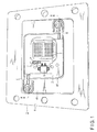
- FIG. 1 to FIG. 9 A light-emitting apparatus according to an embodiment will now be described with reference to FIG. 1 to FIG. 9 . It is to be noted that like reference numerals denote like parts to omit an overlapping description.
- a light-emitting apparatus 1 comprises a substrate 2, light-emitting elements 3, an attachment member 4, and mechanical fixing components 5.
- the light-emitting elements 3 are mounted on a front surface side which is one surface side of the substrate 2.
- the substrate 2 is arranged on the attachment member 4.
- the mechanical fixing components 5 hold the substrate 2 on the attachment member 4.
- the substrate 2 has insulating properties, and it is made of a ceramics material like a whitish aluminum oxide or aluminum nitride.
- the substrate 2 is formed into a substantially square shape which is a polygonal shape. Each corner portion of the substrate has a circular shape.
- a boron nitride, a silicon nitride, a magnesium oxide, forsterite, steatite, low-temperature sintering ceramics, and others can be applied as the material of the substrate 2, and the substrate 2 is not restricted to a specific material in particular. Further, the shape of the substrate 2 is not restricted to the square shape, it may be any other polygonal shape such as a circular shape or a hexagonal shape, and the shape can be appropriately selected in accordance with design.
- a wiring pattern is formed on the front surface side of the substrate 2.
- This wiring pattern is constituted of a feed conductor 21 and a feed terminal 22.
- the feed conductor 21 is constituted of a positive-electrode-side feed conductor 21a and a negative-electrode-side feed conductor 21b.
- the feed terminal 22 is constituted of a positive-electrode-side feed terminal 22a and a negative-electrode-side feed terminal 22b.
- the positive-electrode-side feed conductor 21a is formed to linearly extended at a central portion on the surface of the substrate 2.
- the positive-electrode-side feed terminal 22a is formed at one end portion (a left-hand side in the drawing) of the positive-electrode-side feed conductor 21a to be continuous with the positive-electrode-side feed conductor 21a.
- the negative-electrode-side feed conductor 21b is formed into a square shape to surround the positive-electrode-side feed conductor 21a.
- the positive-electrode-side feed conductor 21a is placed at a central portion of the negative-electrode-side feed conductor 21b.
- the positive-electrode-side feed terminal 22a is formed at one end portion (a lower left side in the drawing) of the positive-electrode-side feed conductor 21a to be continuous with the positive-electrode-side feed conductor 21a.
- lighting inspection conductors 23 for a lighting confirmation test a temperature inspection conductor 24 for temperature measurement, and the like are formed on the surface of the substrate 2.
- Each of the feed conductor 21 and the feed terminal 22 is formed by, for example, screen-printing silver (Ag) or an alloy containing silver (Ag) as a main component on the substrate 2. It is to be noted that each of the feed conductor 21 and the feed terminal 22 may be formed by plate processing in place of screen printing. Furthermore, a metal having excellent conductivity such as copper (Cu) or gold (Au) can be applied as this formation material.
- a protective layer 25 made of an electric insulating material consisting of, for example, glass paste is partially (both left and right sides in the drawing) formed in the wiring pattern.
- This protective layer 25 is formed by the screen printing.
- the protective layer 25 is configured to mainly cover portions of the feed conductor 21 and the feed terminal 22 that are not sealed by a later-described sealing member 27. As a result, deterioration of the feed conductor 21 and the feed terminal 22 can be suppressed.
- the light-emitting elements 3 are mounted on the surface of the substrate 2.
- the light-emitting element 3 is constituted of a bare chip of an LED, and it is directly bonded to the surface of the substrate 2.
- a material that emits blue light is used in order to emit whitish light by a light-emitting portion.
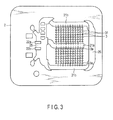
- these light-emitting elements 3 are aligned in a matrix form with the positive-electrode-side feed conductor 21a at the boundary, thereby forming strings (light-emitting element strings).
- the bare chip of the LED is, for example, an InGaN-based element obtained by laminating a light-emitting layer on a translucent sapphire element substrate.
- the light-emitting layer is formed into a substantially rectangular parallelepiped shape by sequentially laminating an n-type-nitride semiconductor layer, an InGaN light-emitting layer, and a p-type-nitride semiconductor layer.
- an electrode configured to pass a current through the light-emitting layer is provided on an upper surface side.
- This electrode is constituted of a positive-side electrode formed of a p-type electrode pad on the p-type-nitride semiconductor layer and a negative-side electrode formed of an n-type electrode pad on the n-type-nitride semiconductor layer. These electrodes are electrically connected to each other through a bonding wire 31.
- the bonding wire 31 is formed of a gold (Au) fine wire.
- Each bonding wire 31 is connected through a bump containing gold (Au) as a main component in order to improve mounting strength and reduce damage to the bare chip of each LED.
- a metal fine wire such as a copper wire, an aluminum wire, or a platinum wire can be applied as the bonding wire 31.
- the bare chips of the LEDs form the light-emitting element strings in a direction extending toward the negative-electrode-side feed conductor 21b facing the positive-electrode-side feed conductor 21a with the positive-electrode-side feed conductor 21 at the boundary. Therefore, in the drawing, the bare chips of the LEDs form an upper matrix block and a lower matrix block.
- each light-emitting element string electrodes with different polarities of the respective light-emitting elements adjacent to each other in a direction along which the string extends, i.e., the positive-side electrode of the one light-emitting element 3 in the light-emitting elements 3 adjacent to each other and the negative-side electrode of the other light-emitting element 3 in the light-emitting elements 3 adjacent to each other are sequentially connected through the bonding wire 31.
- the light-emitting elements 3 constituting each light-emitting element string are electrically connected in series.
- each light-emitting element string the electrode of each light-emitting element 3a arranged at an end of a specific light-emitting element string is connected to the positive-electrode-side feed conductor 21a or the negative-electrode-side feed conductor 21b through the bonding wire 31. Therefore, seven light-emitting elements 3 are connected in series in one light-emitting string.
- the 12 light-emitting element strings are formed in the upper matrix block.
- the 12 light-emitting element strings are formed in the lower matrix block. Therefore, 24 series circuits, each of which has the seven light-emitting elements 3 connected in series, are connected in parallel, whereby the light-emitting elements 3 are operated to simultaneously emit light in an energized state. Therefore, even if any string in the respective light-emitting element strings cannot emit light because of, for example, a bonding failure, light emission of the entire light-emitting apparatus 1 is not stopped.
- a frame member 26 is provided on the surface of the substrate 2.
- This frame member 26 is made of a white synthetic resin and applied in a substantially square shape.
- the respective light-emitting elements 3 are arranged on the inner side of the frame member 26 surrounded by an inner peripheral surface of the frame member 26. That is, a mounting region of the light-emitting elements 3 is surrounded by the frame member 26.
- the inner side of the frame member 26 is filled with the sealing member 27.
- the sealing member 27 is provided on the substrate 2.
- the sealing member 27 is, for example, a translucent synthetic resin like a transparent silicone resin, and it seals the mounting region of the light-emitting elements 3.
- the sealing member 27 contains an appropriate amount of a fluorescent material.
- the fluorescent material is excited by light emitted from the tight-emitting elements 3, and it radiates light having a color different from that of the light emitted from the light-emitting elements 3.
- the light-emitting elements 3 emit blue light, to enable emission of white light, a yellow fluorescent material that radiates yellowish light is used as the fluorescent material.
- the yellowish light has a complementary color relationship with the blue light.
- a predetermined amount of the sealing member 27 is injected into the inner side of the frame member 26 in an unhardened state, and then the sealing member 27 is heat-hardened and provided in this state.
- the connector 6 has a white synthetic resin case having less light absorption properties.
- a pair of terminal pins are protruded from one side surface of the case.
- the terminal pins are soldered and electrically connected to the positive-electrode-side feed terminal 22a and the negative-electrode-side feed terminal 22b.
- a lead wire connected to a power supply side is connected to this connector 6. As a result, electric power is supplied to the respective light-emitting elements 3 through the connector 6.
- the capacitors 7 function to prevent noise from being superimposed on a power supply and then being applied to the respective light-emitting elements 3.
- the thus configured substrate 2 is disposed to the attachment member 4 depicted in FIG. 5 .
- the attachment member 4 is made of, for example, an aluminum material having excellent heat conduction.
- the attachment member 4 has a square shape which is a polygonal shape. Each corner portion of the attachment member 4 has a circular shape.
- the attachment member 4 has a slightly inclined arrangement surface 41 for the substrate 2 at the central portion thereof.
- a concave portion 42 having a substantially square shape in which The substrate 2 is installed is formed in this arrangement surface 41.
- a bottom surface 42a of this concave portion 42 is formed into a flat shape.
- a side surface 42b of the concave portion 42 is formed to erect from the circumference of the bottom surface 42a.
- the concave portion 42 has a shape substantially similar to the outer shape of the substrate 2 and is formed to be slightly larger than the substrate 2. Moreover, substantially-U-shaped positioning protruding portions 43 and screw holes 44 at which the later-described mechanical fixing components 5 are arranged are formed on a diagonal line of the concave portion 42.
- this attachment member 4 may be, for example, a heat sink, a main body of an apparatus, a case, or a cover. In short, this means a member to which the substrate 2 is disposed.
- the substrate 2 is positioned and arranged with the concave portion 42 of the attachment member 4 being used as a guide.
- the substrate 2 is disposed in such a manner that its back surface side which is the other surface side is appressed against the bottom surface 42a of the attachment member 4. That is, the mechanical fixing components 5 give elastic pressing force in a direction extending from the front surface side toward the back surface side of the substrate 2, thereby disposing the substrate 2.
- the concave portion 42 has the shape substantially similar to the outer shape of the substrate 2 and is formed to be slightly larger than the substrate 2, and hence positioning of the substrate 2 can be facilitated.
- the mechanical fixing component 5 is a fixing member having a leaf spring shape.
- the mechanical fixing component 5 is positioned to each positioning protruding portion 43 from the front surface (upper surface) side of the attachment member 4.
- the mechanical fixing component 5 is configured to be fixed on the front surface of the attachment member 4 by a fixing component such as a screw. Therefore, the pair of mechanical fixing components 5 are arranged on the substantially diagonal line of the substrate 2.
- the fixing member 5 is made of a metal plate-like material.
- This fixing member 5 is made of stainless steel having elasticity.
- This fixing member 5 has a base portion 51, a pressure portion 52, and a protective portion 53.
- the base portion 51 has a predetermined width dimension, and a through-hole in which fixing component such as a screw is inserted is formed in the base portion 51.
- the pressure portion 52 having a narrow width is extended from a substantially central portion of this base portion 51. In the drawing, this pressure portion 52 is formed to be bent in order to apply elastic pressing force in a page space direction. An end side of the pressure portion 52 is configured to come into contact with the front surface side of the substrate 2.
- the protective portion 53 is extended parallel to the pressure portion 52.
- the protective portion 53 has a width larger than that of the pressure portion 52 and is linearly extended. This protective portion 53 can be gripped when handling the fixing member 5 in an assembling operation and the like.
- the protective portion 53 has a function of avoiding, for example, deformation of the pressure portion 52 when external force is applied thereto and also protecting the pressure portion 52. If the protective portion 53 is not provided, the pressure portion 52 is gripped and handled, and inconvenience, for example, the deformation of the pressure portion 52 may possibly occur.
- an extended length dimension of the protective portion 53 is preferable. As a result, the pressure portion 52 is assuredly protected.
- a gap G is formed between a side periphery of the substrate 2 and the side surface 42b of the concave portion 42. Specifically, the gap G of approximately 1 mm is formed over the whole circumference of the substrate 2.
- this gap G is not restricted in particular. Moreover, it is preferable for the gap G to be uniform over the whole circumference of the substrate 2, but the gap G does not have to be necessarily uniform. For example, a part of the side circumference of the substrate 2 may be in contact with the side surface 42b of the concave portion 42. In short, when the substrate 2 can move in the horizontal direction as will be described later, providing the gap G that can absorb thermal expansion of the substrate 2 can suffice. Additionally, an elastic material such as a cushion member may be interposed in this gap G. In such a case, the thermal expansion of the substrate 2 can be likewise absorbs.
- the mechanical fixing components 5 are disposed on the front surface side corresponding to a higher position than the bottom surface 42a of the concave portion 42 in the attachment member 4.
- Each pressure portion 52 is in contact with the one surface side of the substrate 2 at a position on the bottom surface 42a side of the concave portion 42 apart from the front surface side of the attachment member 4. That is, in a state that the fixing member 5 is being fixed to the attachment member 4, the end side of each pressure portion 52 is in contact with the front surface of the substrate 2 to have a step S on a lower side (the concave portion 42 side) of the upper surface of the attachment member 4. Therefore, the elastic pressing force of each pressure portion 52 effectively acts on the front surface of the substrate 2, and predetermined elastic pressing force can be maintained across the age.
- This elastic pressing force (the elastic load) can be realized by setting the step S to 0.1 mm to 0.6 mm. That is, the elastic pressing force (the elastic load) is increased when the step S is small, and the elastic pressing force (the elastic load) is reduced when the step S is large.
- FIG. 8 and FIG. 9 show examples when the dimension of the step S is adjusted to set the elastic pressing force (the elastic load).
- the dimension of the step S is reduced, whereby the elastic pressing force (the elastic load) is set to 350 g. In this case, the dimension of the step S is adjusted to, for example, 0.1 mm.
- the dimension of the step S is increased, whereby the elastic pressing force (the elastic load) is set to 180 g. In this case, the dimension of the step S is adjusted to, for example, 0.6 mm.
- a depth dimension of the concave portion 42 is coordinated to adjust the dimension of the step S
- the adjustment is not restricted to this conformation.
- the dimension of the step S can be likewise adjusted by, for example, coordinating a thickness dimension of the substrate 2.
- the elastic pressing force (the elastic load) can be appropriately set in accordance with design.
- a thermally conductive member 8 is interposed between the back surface side of the substrate 2 and the bottom surface 42a of the concave portion 42.
- adhesion of the substrate 2 and the bottom surface 42a of the concave portion 42 can be improved, and heat from the substrate 2 can be conducted to the attachment member 4, thereby facilitating heat radiation.
- the thermally conductive member 8 is grease having predetermined viscosity and flowability, and it is provided by being applied to the bottom surface 42a of the concave portion 42.
- each light-emitting element 3 heat generated from each light-emitting element 3 is mainly conducted to the attachment member 4 from the back surface side of the substrate 2 through the thermally conductive member 8, thereby effecting heat radiation.
- light traveling toward the substrate 2 side in the light emitted from the light-emitting elements 3 are mainly reflected in a light utilizing direction by the surface of the whitish substrate 2.
- the substrate 2 repeats thermal expansion and contraction.
- the substrate 2 is held on the attachment member 4 by the elastic pressing force of the mechanical fixing components 5 rather than fixation, for example, screwing.
- the gap G is formed between the side circumference of the substrate 2 and the side surface 42b of the concave portion 42.
- thermal expansion of the substrate 2 can be absorbed by this gap G, and hence it is possible to suppress generation of cracks in the substrate 2 made of ceramics when stress is applied to the substrate 2.
- the substrate 2 is not fixed by, for example, screwing and it is configured to allow movement (free movement) in the vertical direction and the horizontal direction. As a result, damage such as cracks in the substrate 2 can be suppressed.
- the thermally conductive member 8 enhances the adhesion of the substrate 2 and the bottom surface 42a of the concave portion 42. Moreover, the thermally conductive member 8 functions to smoother movement of the substrate 2 in the horizontal direction while improving the adhesion by the viscosity and the flowability of the thermally conductive member 8.
- the end side of the pressure portion 52 in each mechanical fixing component 5 is in contact with the front surface of the substrate 2 to have the step S on the lower side of the upper surface of the attachment member 4.
- the elastic pressing force of the pressure portion 52 effectively acts on the front surface of the substrate 2, and the predetermined elastic pressing force can be maintained across the ages.
- each corner portion of the substrate 2 has the circular shape and is rounded, breakage due to the external force can be suppressed. For example, when handling the substrate 2 in an assembling operation and the like, the breakage due to the external force can be effectively avoided.
- the substrate 2 since the free movement of the substrate 2 is allowed in the concave portion 42, the substrate 2 may freely move in the concave portion 42 because of vibration and other factors. Even in such a case, since each corner portion of the substrate 2 has the circular shape, the breakage can be effectively suppressed.
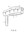
- FIG. 10 shows a road lighting unit 10 which is an illumination apparatus having the light-emitting apparatuses 1 arranged therein.
- the road lighting unit 10 is configured by disposing a lamp fitting 12 to an upper end portion of a column 11.
- the column 11 is installed alongside a road.
- a road is illuminated with light emitted from the lamp fitting 12.
- the light-emitting apparatuses 1 are arranged in the lamp fitting 12. Light from the light-emitting apparatus 1 are radiated through a translucent cover 13.
- the light-emitting apparatus 1 functions and effects exhibited by the light-emitting apparatus 1 can be realized. Furthermore, in particular, the light-emitting apparatuses 1 are placed in an environment where they easily undergo vibration, but damage to the substrate 2 can be suppressed in this case.
- the present invention is not restricted to the configuration of the foregoing embodiment, and it can be modified in many ways without departing from the gist of the present invention.
- a metal base substrate having an insulating layer laminated on one surface of a base plate which has excellent heat conduction properties and is superior in heat radiation properties like aluminum. In this case, an effect of suppressing deformation of the substrate can be expected.
- a solid light-emitting element such as an LED can be applied as the light-emitting element.
- the number of the light-emitting elements to be mounted is not restricted in particular.
- the light-emitting apparatus can be incorporated into a road lighting unit, an illumination apparatus for vehicles, a light source as an LED lamp, various kinds of lighting fittings used in or out of doors, or an apparatus main body of a display apparatus and the like, thereby configuring as an illumination apparatus.
Landscapes
- Engineering & Computer Science (AREA)
- General Engineering & Computer Science (AREA)
- Physics & Mathematics (AREA)
- Microelectronics & Electronic Packaging (AREA)
- Optics & Photonics (AREA)
- Led Device Packages (AREA)
- Non-Portable Lighting Devices Or Systems Thereof (AREA)
- Led Devices (AREA)
- Fastening Of Light Sources Or Lamp Holders (AREA)
Abstract
Description
- Embodiments described herein relate generally to a light-emitting apparatus using light-emitting elements like LEDs and an illumination apparatus including this light-emitting apparatus.
- An LED is used as a light source of an illumination apparatus. This light source is constituted as a light-emitting apparatus in which bare chips of many LEDs are mounted on a substrate, the respective LED chips are electrically connected to each other through bonding wires, and the substrate is fixed to an attachment member by fixing components such as screws.
- In recent years, in such a light-emitting apparatus, a high output has been demanded. To realize this high output, a current supplied to the LEDs must be increased. However, when the current to be supplied is increased, a temperature of the LEDs rises, and the LEDs are operated at a high temperature. In consequence, a temperature of the substrate is also increased, and hence a difference between thermal expansion and contraction of the substrate becomes large in a thermo-cycle of on/off of the LEDs.
- In the above-described configuration, when the substrate is fixed to the attachment member with fixing components such as screws, stress is applied to the substrate because of a difference in heat characteristics such as a difference in thermal expansion coefficient between the substrate and the attachment member. As a result, the substrate may be deformed or cracked, whereby the substrate may be possibly damaged.
-
-
FIG. 1 is a perspective view showing a light-emitting apparatus according to an embodiment; -
FIG. 2 is a plan view showing a wiring pattern on a substrate in the light-emitting apparatus; -
FIG. 3 is a plan view showing a state that light-emitting elements are mounted on the substrate in the light-emitting apparatus; -
FIG. 4 is a partially cutaway plan view showing a completed state of the substrate in the light-emitting apparatus; -
FIG. 5 is a perspective view showing an attachment member of the light-emitting apparatus; -
FIG. 6 is a perspective view showing the mechanical fixing component; -
FIG. 7 is a cross-sectional view of the light-emitting apparatus taken along line X-X inFIG. 1 ; -
FIG. 8 is a cross-sectional view showing a part of a modification in a fixed state of the substrate; -
FIG. 9 is a cross-sectional view likewise showing a part of a modification in the fixed state of the substrate; and -
FIG. 10 is a perspective view showing an illumination apparatus according to an embodiment. - In general, according to one embodiment, a light-emitting apparatus comprises a substrate, an attachment member, and a mechanical fixing component. The substrate has light-emitting elements mounted on one surface side thereof. The attachment member comprises a concave portion in which the substrate is arranged with a gap between the substrate and a side circumference of the concave portion. The mechanical fixing component comprises a pressure portion that is in contact with the one surface side of the substrate, the mechanical fixing component being configured to hold the substrate in the concave portion of the attachment member by elastic pressing force of the pressure portion acting in a direction from the one surface side toward the other surface side of the substrate.
- A light-emitting apparatus according to an embodiment will now be described with reference to
FIG. 1 to FIG. 9 . It is to be noted that like reference numerals denote like parts to omit an overlapping description. - As representatively shown in
FIG. 1 andFIG. 7 , a light-emitting apparatus 1 comprises asubstrate 2, light-emitting elements 3, anattachment member 4, andmechanical fixing components 5. The light-emittingelements 3 are mounted on a front surface side which is one surface side of thesubstrate 2. Thesubstrate 2 is arranged on theattachment member 4. Themechanical fixing components 5 hold thesubstrate 2 on theattachment member 4. - The
substrate 2 has insulating properties, and it is made of a ceramics material like a whitish aluminum oxide or aluminum nitride. Thesubstrate 2 is formed into a substantially square shape which is a polygonal shape. Each corner portion of the substrate has a circular shape. - It is to be noted that a boron nitride, a silicon nitride, a magnesium oxide, forsterite, steatite, low-temperature sintering ceramics, and others can be applied as the material of the
substrate 2, and thesubstrate 2 is not restricted to a specific material in particular. Further, the shape of thesubstrate 2 is not restricted to the square shape, it may be any other polygonal shape such as a circular shape or a hexagonal shape, and the shape can be appropriately selected in accordance with design. - As shown in
FIG. 2 , a wiring pattern is formed on the front surface side of thesubstrate 2. This wiring pattern is constituted of afeed conductor 21 and afeed terminal 22. Thefeed conductor 21 is constituted of a positive-electrode-side feed conductor 21a and a negative-electrode-side feed conductor 21b. Thefeed terminal 22 is constituted of a positive-electrode-side feed terminal 22a and a negative-electrode-side feed terminal 22b. - The positive-electrode-
side feed conductor 21a is formed to linearly extended at a central portion on the surface of thesubstrate 2. The positive-electrode-side feed terminal 22a is formed at one end portion (a left-hand side in the drawing) of the positive-electrode-side feed conductor 21a to be continuous with the positive-electrode-side feed conductor 21a. - The negative-electrode-
side feed conductor 21b is formed into a square shape to surround the positive-electrode-side feed conductor 21a. The positive-electrode-side feed conductor 21a is placed at a central portion of the negative-electrode-side feed conductor 21b. The positive-electrode-side feed terminal 22a is formed at one end portion (a lower left side in the drawing) of the positive-electrode-side feed conductor 21a to be continuous with the positive-electrode-side feed conductor 21a. - It is to be noted that, although the detailed description will be omitted,
lighting inspection conductors 23 for a lighting confirmation test, atemperature inspection conductor 24 for temperature measurement, and the like are formed on the surface of thesubstrate 2. - Each of the
feed conductor 21 and thefeed terminal 22 is formed by, for example, screen-printing silver (Ag) or an alloy containing silver (Ag) as a main component on thesubstrate 2. It is to be noted that each of thefeed conductor 21 and thefeed terminal 22 may be formed by plate processing in place of screen printing. Furthermore, a metal having excellent conductivity such as copper (Cu) or gold (Au) can be applied as this formation material. - As representatively shown in
FIG. 3 , aprotective layer 25 made of an electric insulating material consisting of, for example, glass paste is partially (both left and right sides in the drawing) formed in the wiring pattern. Thisprotective layer 25 is formed by the screen printing. Theprotective layer 25 is configured to mainly cover portions of thefeed conductor 21 and thefeed terminal 22 that are not sealed by a later-describedsealing member 27. As a result, deterioration of thefeed conductor 21 and thefeed terminal 22 can be suppressed. - The light-emitting
elements 3 are mounted on the surface of thesubstrate 2. The light-emittingelement 3 is constituted of a bare chip of an LED, and it is directly bonded to the surface of thesubstrate 2. As the bare chip of the LED, for example, a material that emits blue light is used in order to emit whitish light by a light-emitting portion. - As shown in
FIG. 3 , these light-emitting elements 3 are aligned in a matrix form with the positive-electrode-side feed conductor 21a at the boundary, thereby forming strings (light-emitting element strings). - The bare chip of the LED is, for example, an InGaN-based element obtained by laminating a light-emitting layer on a translucent sapphire element substrate. The light-emitting layer is formed into a substantially rectangular parallelepiped shape by sequentially laminating an n-type-nitride semiconductor layer, an InGaN light-emitting layer, and a p-type-nitride semiconductor layer. Moreover, an electrode configured to pass a current through the light-emitting layer is provided on an upper surface side. This electrode is constituted of a positive-side electrode formed of a p-type electrode pad on the p-type-nitride semiconductor layer and a negative-side electrode formed of an n-type electrode pad on the n-type-nitride semiconductor layer. These electrodes are electrically connected to each other through a
bonding wire 31. The bondingwire 31 is formed of a gold (Au) fine wire. Eachbonding wire 31 is connected through a bump containing gold (Au) as a main component in order to improve mounting strength and reduce damage to the bare chip of each LED. It is to be noted that a metal fine wire such as a copper wire, an aluminum wire, or a platinum wire can be applied as thebonding wire 31. - Specifically, the bare chips of the LEDs form the light-emitting element strings in a direction extending toward the negative-electrode-
side feed conductor 21b facing the positive-electrode-side feed conductor 21a with the positive-electrode-side feed conductor 21 at the boundary. Therefore, in the drawing, the bare chips of the LEDs form an upper matrix block and a lower matrix block. - In each light-emitting element string, electrodes with different polarities of the respective light-emitting elements adjacent to each other in a direction along which the string extends, i.e., the positive-side electrode of the one light-emitting
element 3 in the light-emittingelements 3 adjacent to each other and the negative-side electrode of the other light-emittingelement 3 in the light-emittingelements 3 adjacent to each other are sequentially connected through thebonding wire 31. As a result, the light-emittingelements 3 constituting each light-emitting element string are electrically connected in series. - Additionally, in each light-emitting element string, the electrode of each light-emitting
element 3a arranged at an end of a specific light-emitting element string is connected to the positive-electrode-side feed conductor 21a or the negative-electrode-side feed conductor 21b through thebonding wire 31. Therefore, seven light-emittingelements 3 are connected in series in one light-emitting string. The 12 light-emitting element strings are formed in the upper matrix block. Likewise, the 12 light-emitting element strings are formed in the lower matrix block. Therefore, 24 series circuits, each of which has the seven light-emittingelements 3 connected in series, are connected in parallel, whereby the light-emittingelements 3 are operated to simultaneously emit light in an energized state. Therefore, even if any string in the respective light-emitting element strings cannot emit light because of, for example, a bonding failure, light emission of the entire light-emitting apparatus 1 is not stopped. - As shown in
FIG. 4 , aframe member 26 is provided on the surface of thesubstrate 2. Thisframe member 26 is made of a white synthetic resin and applied in a substantially square shape. The respective light-emittingelements 3 are arranged on the inner side of theframe member 26 surrounded by an inner peripheral surface of theframe member 26. That is, a mounting region of the light-emittingelements 3 is surrounded by theframe member 26. - The inner side of the
frame member 26 is filled with the sealingmember 27. The sealingmember 27 is provided on thesubstrate 2. The sealingmember 27 is, for example, a translucent synthetic resin like a transparent silicone resin, and it seals the mounting region of the light-emittingelements 3. - Further, the sealing
member 27 contains an appropriate amount of a fluorescent material. The fluorescent material is excited by light emitted from the tight-emittingelements 3, and it radiates light having a color different from that of the light emitted from the light-emittingelements 3. In this embodiment that the light-emittingelements 3 emit blue light, to enable emission of white light, a yellow fluorescent material that radiates yellowish light is used as the fluorescent material. The yellowish light has a complementary color relationship with the blue light. A predetermined amount of the sealingmember 27 is injected into the inner side of theframe member 26 in an unhardened state, and then the sealingmember 27 is heat-hardened and provided in this state. - Furthermore, a
connector 6 and twocapacitors 7 are mounted on the surface of thesubstrate 2. Theconnector 6 has a white synthetic resin case having less light absorption properties. A pair of terminal pins are protruded from one side surface of the case. The terminal pins are soldered and electrically connected to the positive-electrode-side feed terminal 22a and the negative-electrode-side feed terminal 22b. Moreover, a lead wire connected to a power supply side is connected to thisconnector 6. As a result, electric power is supplied to the respective light-emittingelements 3 through theconnector 6. - The
capacitors 7 function to prevent noise from being superimposed on a power supply and then being applied to the respective light-emittingelements 3. - The thus configured
substrate 2 is disposed to theattachment member 4 depicted inFIG. 5 . Theattachment member 4 is made of, for example, an aluminum material having excellent heat conduction. Theattachment member 4 has a square shape which is a polygonal shape. Each corner portion of theattachment member 4 has a circular shape. Theattachment member 4 has a slightlyinclined arrangement surface 41 for thesubstrate 2 at the central portion thereof. Aconcave portion 42 having a substantially square shape in which Thesubstrate 2 is installed is formed in thisarrangement surface 41. Abottom surface 42a of thisconcave portion 42 is formed into a flat shape. Aside surface 42b of theconcave portion 42 is formed to erect from the circumference of thebottom surface 42a. Theconcave portion 42 has a shape substantially similar to the outer shape of thesubstrate 2 and is formed to be slightly larger than thesubstrate 2. Moreover, substantially-U-shapedpositioning protruding portions 43 and screwholes 44 at which the later-describedmechanical fixing components 5 are arranged are formed on a diagonal line of theconcave portion 42. - Additionally, screw through-holes used for fixing this
attachment member 4 to, for example, a main body of an illumination apparatus are formed on both sides of theattachment member 4. It is to be noted that thisattachment member 4 may be, for example, a heat sink, a main body of an apparatus, a case, or a cover. In short, this means a member to which thesubstrate 2 is disposed. - As shown in
FIG. 1 andFIG. 7 , thesubstrate 2 is positioned and arranged with theconcave portion 42 of theattachment member 4 being used as a guide. Thesubstrate 2 is disposed in such a manner that its back surface side which is the other surface side is appressed against thebottom surface 42a of theattachment member 4. That is, themechanical fixing components 5 give elastic pressing force in a direction extending from the front surface side toward the back surface side of thesubstrate 2, thereby disposing thesubstrate 2. It is to be noted that theconcave portion 42 has the shape substantially similar to the outer shape of thesubstrate 2 and is formed to be slightly larger than thesubstrate 2, and hence positioning of thesubstrate 2 can be facilitated. - The
mechanical fixing component 5 is a fixing member having a leaf spring shape. Themechanical fixing component 5 is positioned to eachpositioning protruding portion 43 from the front surface (upper surface) side of theattachment member 4. Themechanical fixing component 5 is configured to be fixed on the front surface of theattachment member 4 by a fixing component such as a screw. Therefore, the pair ofmechanical fixing components 5 are arranged on the substantially diagonal line of thesubstrate 2. - As representatively shown in
FIG. 6 , the fixingmember 5 is made of a metal plate-like material. This fixingmember 5 is made of stainless steel having elasticity. This fixingmember 5 has abase portion 51, apressure portion 52, and aprotective portion 53. Thebase portion 51 has a predetermined width dimension, and a through-hole in which fixing component such as a screw is inserted is formed in thebase portion 51. Thepressure portion 52 having a narrow width is extended from a substantially central portion of thisbase portion 51. In the drawing, thispressure portion 52 is formed to be bent in order to apply elastic pressing force in a page space direction. An end side of thepressure portion 52 is configured to come into contact with the front surface side of thesubstrate 2. - Furthermore, the
protective portion 53 is extended parallel to thepressure portion 52. Theprotective portion 53 has a width larger than that of thepressure portion 52 and is linearly extended. Thisprotective portion 53 can be gripped when handling the fixingmember 5 in an assembling operation and the like. Theprotective portion 53 has a function of avoiding, for example, deformation of thepressure portion 52 when external force is applied thereto and also protecting thepressure portion 52. If theprotective portion 53 is not provided, thepressure portion 52 is gripped and handled, and inconvenience, for example, the deformation of thepressure portion 52 may possibly occur. - It is to be noted that forming an extended length dimension of the
protective portion 53 to be equal to or longer than an extended length dimension of thepressure portion 52 is preferable. As a result, thepressure portion 52 is assuredly protected. - As shown in
FIG. 7 , in a state that thensubstrate 2 is arranged in theconcave portion 42 and held by themechanical fixing components 5, a gap G is formed between a side periphery of thesubstrate 2 and theside surface 42b of theconcave portion 42. Specifically, the gap G of approximately 1 mm is formed over the whole circumference of thesubstrate 2. - It is to be noted that a dimension of this gap G is not restricted in particular. Moreover, it is preferable for the gap G to be uniform over the whole circumference of the
substrate 2, but the gap G does not have to be necessarily uniform. For example, a part of the side circumference of thesubstrate 2 may be in contact with theside surface 42b of theconcave portion 42. In short, when thesubstrate 2 can move in the horizontal direction as will be described later, providing the gap G that can absorb thermal expansion of thesubstrate 2 can suffice. Additionally, an elastic material such as a cushion member may be interposed in this gap G. In such a case, the thermal expansion of thesubstrate 2 can be likewise absorbs. - Further, the
mechanical fixing components 5 are disposed on the front surface side corresponding to a higher position than thebottom surface 42a of theconcave portion 42 in theattachment member 4. Eachpressure portion 52 is in contact with the one surface side of thesubstrate 2 at a position on thebottom surface 42a side of theconcave portion 42 apart from the front surface side of theattachment member 4. That is, in a state that the fixingmember 5 is being fixed to theattachment member 4, the end side of eachpressure portion 52 is in contact with the front surface of thesubstrate 2 to have a step S on a lower side (theconcave portion 42 side) of the upper surface of theattachment member 4. Therefore, the elastic pressing force of eachpressure portion 52 effectively acts on the front surface of thesubstrate 2, and predetermined elastic pressing force can be maintained across the age. Furthermore, it is possible to reduce application of excessive stress to a part of the fixingmember 5 fixed by, for example, a screw. As a result, the elastic pressing force of thepressure portion 52 of the fixingmember 5 in the direction from the front surface side to the back surface side of thensubstrate 2 is applied to thesubstrate 2, thereby holding thesubstrate 2 on theattachment member 4. - It is preferable to set the elastic pressing force (an elastic load) of the
mechanical fixing components 5 to 180 g to 350 g. This elastic pressing force (the elastic load) can be realized by setting the step S to 0.1 mm to 0.6 mm. That is, the elastic pressing force (the elastic load) is increased when the step S is small, and the elastic pressing force (the elastic load) is reduced when the step S is large. -
FIG. 8 and FIG. 9 show examples when the dimension of the step S is adjusted to set the elastic pressing force (the elastic load). InFIG. 8 , the dimension of the step S is reduced, whereby the elastic pressing force (the elastic load) is set to 350 g. In this case, the dimension of the step S is adjusted to, for example, 0.1 mm. InFIG. 9 , the dimension of the step S is increased, whereby the elastic pressing force (the elastic load) is set to 180 g. In this case, the dimension of the step S is adjusted to, for example, 0.6 mm. - In these cases, although a depth dimension of the
concave portion 42 is coordinated to adjust the dimension of the step S, the adjustment is not restricted to this conformation. For example, the dimension of the step S can be likewise adjusted by, for example, coordinating a thickness dimension of thesubstrate 2. When the dimension of the step S is adjusted in this manner, the elastic pressing force (the elastic load) can be appropriately set in accordance with design. - Moreover, a thermally
conductive member 8 is interposed between the back surface side of thesubstrate 2 and thebottom surface 42a of theconcave portion 42. As a result, adhesion of thesubstrate 2 and thebottom surface 42a of theconcave portion 42 can be improved, and heat from thesubstrate 2 can be conducted to theattachment member 4, thereby facilitating heat radiation. Specifically, the thermallyconductive member 8 is grease having predetermined viscosity and flowability, and it is provided by being applied to thebottom surface 42a of theconcave portion 42. - When electric power is supplied to the thus configured light-emitting apparatus 1 by a lighting circuit, energization is carried out from the
connector 6 through the positive-electrode-side feed terminal 22a, the positive-electrode-side feed conductor 21a, thebonding wires 31, the light-emittingelements 3, and the negative-electrode-side feed conductor 21b, and it further performed from the negative-electrode-side feed terminal 22b to theconnector 6. As a result, the respective light-emittingelements 3 covered with the sealingmember 27 are simultaneously operated to emit light, and the light-emitting apparatus 1 is used as a planar light source that emits white light. - During this lighting, heat generated from each light-emitting
element 3 is mainly conducted to theattachment member 4 from the back surface side of thesubstrate 2 through the thermallyconductive member 8, thereby effecting heat radiation. Moreover, during the lighting of the light-emitting apparatus 1, light traveling toward thesubstrate 2 side in the light emitted from the light-emittingelements 3 are mainly reflected in a light utilizing direction by the surface of thewhitish substrate 2. - Additionally, in a thermo-cycle of on/off the light-emitting
elements 3, thesubstrate 2 repeats thermal expansion and contraction. However, thesubstrate 2 is held on theattachment member 4 by the elastic pressing force of themechanical fixing components 5 rather than fixation, for example, screwing. The gap G is formed between the side circumference of thesubstrate 2 and theside surface 42b of theconcave portion 42. As a result, thermal expansion of thesubstrate 2 can be absorbed by this gap G, and hence it is possible to suppress generation of cracks in thesubstrate 2 made of ceramics when stress is applied to thesubstrate 2. Additionally, it is also possible to suppress generation of cracks in thesubstrate 2 when, for example, tightening force using screws and the like directly acts on thesubstrate 2. - Further, it is possible to absorb vertical stress and horizontal stress applied to the
substrate 2 because of, for example, thermal expansion or vibration of thesubstrate 2. That is because thesubstrate 2 is not fixed by, for example, screwing and it is configured to allow movement (free movement) in the vertical direction and the horizontal direction. As a result, damage such as cracks in thesubstrate 2 can be suppressed. - Furthermore, the thermally
conductive member 8 enhances the adhesion of thesubstrate 2 and thebottom surface 42a of theconcave portion 42. Moreover, the thermallyconductive member 8 functions to smoother movement of thesubstrate 2 in the horizontal direction while improving the adhesion by the viscosity and the flowability of the thermallyconductive member 8. - Additionally, the end side of the
pressure portion 52 in eachmechanical fixing component 5 is in contact with the front surface of thesubstrate 2 to have the step S on the lower side of the upper surface of theattachment member 4. As a result, the elastic pressing force of thepressure portion 52 effectively acts on the front surface of thesubstrate 2, and the predetermined elastic pressing force can be maintained across the ages. - Further, for example, if acute corner portion remain in the
substrate 2 made of ceramics as they are, the corner portions of thesubstrate 2 may be easily broken and destroyed when external force is applied because of, for example, impact shock. However, in this embodiment, each corner portion of thesubstrate 2 has the circular shape and is rounded, breakage due to the external force can be suppressed. For example, when handling thesubstrate 2 in an assembling operation and the like, the breakage due to the external force can be effectively avoided. - Furthermore, since the free movement of the
substrate 2 is allowed in theconcave portion 42, thesubstrate 2 may freely move in theconcave portion 42 because of vibration and other factors. Even in such a case, since each corner portion of thesubstrate 2 has the circular shape, the breakage can be effectively suppressed. -
FIG. 10 shows aroad lighting unit 10 which is an illumination apparatus having the light-emitting apparatuses 1 arranged therein. Theroad lighting unit 10 is configured by disposing a lamp fitting 12 to an upper end portion of acolumn 11. Thecolumn 11 is installed alongside a road. A road is illuminated with light emitted from thelamp fitting 12. The light-emitting apparatuses 1 are arranged in thelamp fitting 12. Light from the light-emitting apparatus 1 are radiated through atranslucent cover 13. - According to such an illumination apparatus, functions and effects exhibited by the light-emitting apparatus 1 can be realized. Furthermore, in particular, the light-emitting apparatuses 1 are placed in an environment where they easily undergo vibration, but damage to the
substrate 2 can be suppressed in this case. - It is to be noted that the present invention is not restricted to the configuration of the foregoing embodiment, and it can be modified in many ways without departing from the gist of the present invention. For example, it is possible to apply a metal base substrate having an insulating layer laminated on one surface of a base plate which has excellent heat conduction properties and is superior in heat radiation properties like aluminum. In this case, an effect of suppressing deformation of the substrate can be expected. Additionally, a solid light-emitting element such as an LED can be applied as the light-emitting element. Further, the number of the light-emitting elements to be mounted is not restricted in particular.
- Furthermore, the light-emitting apparatus according to the foregoing embodiment can be incorporated into a road lighting unit, an illumination apparatus for vehicles, a light source as an LED lamp, various kinds of lighting fittings used in or out of doors, or an apparatus main body of a display apparatus and the like, thereby configuring as an illumination apparatus.
- While certain embodiments have been described, these embodiments have been presented by way of example only, and are not intended to limit the scope of the inventions. Indeed, the novel embodiments described herein may be embodied in a variety of other forms; furthermore, various omissions, substitutions and changes in the form of the embodiments described herein may be made without departing from the spirit of the inventions. The accompanying claims and their equivalents are intended to cover such forms or modifications as would fall within the scope and spirit of the inventions.
Claims (5)
- A light-emitting apparatus (1) characterized by comprising:a substrate (2) which has light-emitting elements (3) mounted on one surface side thereof;an attachment member (4) comprising a concave portion (42) in which the substrate (2) is arranged with a gap (G) between the substrate (2) and a side circumference (42b) of the concave portion (42); anda mechanical fixing component (5) which comprises a pressure portion (52) that is in contact with the one surface side of the substrate (2), the mechanical fixing component (5) being configured to hold the substrate (2) in the concave portion (42) of the attachment member (4) by elastic pressing force of the pressure portion (52) acting in a direction from the one surface side toward the other surface side of the substrate (2).
- The apparatus (1) of claim 1, characterized in that the mechanical fixing component (5) is disposed on a surface side corresponding to a position higher than a bottom surface (42a) of the concave portion (42) of the attachment member (4), and
the pressure portion (52) is in contact with the one surface side of the substrate (2) at a position on the bottom surface (42a) side of the concave portion (42) apart from the surface side of the attachment member (4). - The apparatus of claim 1 or 2, characterized in that the mechanical fixing component (5) is made of a metal plate-like material having elasticity and comprises a base portion (51), the pressure portion (52) extended from the base portion (51), and a protective portion (53) extended parallel to the pressure portion (52).
- The apparatus of any one of claims 1 to 3, characterized in that the substrate (2) is made of ceramics and formed into a polygonal shape comprising circular corner portions.
- An illumination apparatus (10) characterized by comprising:an apparatus main body (12); andthe light-emitting apparatus (1) of any one of claims 1 to 4 arranged in the apparatus main (12) body.
Applications Claiming Priority (1)
| Application Number | Priority Date | Filing Date | Title |
|---|---|---|---|
| JP2010171218A JP5487396B2 (en) | 2010-07-29 | 2010-07-29 | Light emitting device and lighting device |
Publications (3)
| Publication Number | Publication Date |
|---|---|
| EP2413021A2 true EP2413021A2 (en) | 2012-02-01 |
| EP2413021A3 EP2413021A3 (en) | 2013-04-10 |
| EP2413021B1 EP2413021B1 (en) | 2015-05-06 |
Family
ID=44651044
Family Applications (1)
| Application Number | Title | Priority Date | Filing Date |
|---|---|---|---|
| EP20110175334 Not-in-force EP2413021B1 (en) | 2010-07-29 | 2011-07-26 | Light-emitting apparatus and illumination apparatus |
Country Status (4)
| Country | Link |
|---|---|
| US (1) | US8727568B2 (en) |
| EP (1) | EP2413021B1 (en) |
| JP (1) | JP5487396B2 (en) |
| CN (1) | CN102347425B (en) |
Cited By (7)
| Publication number | Priority date | Publication date | Assignee | Title |
|---|---|---|---|---|
| WO2013174766A1 (en) * | 2012-05-21 | 2013-11-28 | Osram Gmbh | Mounting device for lighting sources and associated method |
| ITMI20121014A1 (en) * | 2012-06-12 | 2013-12-13 | Arditi Spa | LED CHIP ARRAY LIGHTING DEVICE WITH HIGH PRECISION AND RELIABILITY TEMPERATURE DETECTION. |
| EP2712283A1 (en) * | 2012-09-24 | 2014-03-26 | Toshiba Lighting & Technology Corporation | Light-emitting apparatus and luminaire |
| WO2014072158A1 (en) * | 2012-11-09 | 2014-05-15 | Osram Gmbh | Lighting device, and illuminating device comprising the lighting device |
| EP2918906A1 (en) * | 2014-03-12 | 2015-09-16 | TE Connectivity Nederland B.V. | Socket assembly and clamp for a socket assembly |
| EP2757316A3 (en) * | 2013-01-11 | 2016-04-06 | Siteco Beleuchtungstechnik GmbH | Luminaire body |
| DE102016104426A1 (en) * | 2016-03-10 | 2017-09-14 | Trilux Gmbh & Co. Kg | Module for modular outdoor light |
Families Citing this family (12)
| Publication number | Priority date | Publication date | Assignee | Title |
|---|---|---|---|---|
| JP5772657B2 (en) * | 2012-02-27 | 2015-09-02 | 豊田合成株式会社 | Light emitting module |
| US9024514B2 (en) | 2012-02-27 | 2015-05-05 | Toyoda Gosei Co., Ltd. | Light-emitting module having connection member to press for direct electrical contact |
| JP5909702B2 (en) * | 2012-07-31 | 2016-04-27 | パナソニックIpマネジメント株式会社 | lighting equipment |
| JP6057161B2 (en) * | 2012-12-13 | 2017-01-11 | 東芝ライテック株式会社 | Light emitting device |
| CN105264283B (en) | 2013-01-10 | 2018-06-12 | 莫列斯公司 | L ED assembly |
| JP6303949B2 (en) * | 2013-11-29 | 2018-04-04 | 日亜化学工業株式会社 | Light emitting device and lighting apparatus |
| TWI613391B (en) * | 2014-04-01 | 2018-02-01 | 晶元光電股份有限公司 | Light-emitting diode assembly and light-emitting diode bulb using the same |
| JP6372257B2 (en) * | 2014-08-29 | 2018-08-15 | 東芝ライテック株式会社 | LIGHT EMITTING MODULE FOR VEHICLE, LIGHTING DEVICE FOR VEHICLE, AND VEHICLE LIGHT |
| JP2019080688A (en) * | 2017-10-30 | 2019-05-30 | 株式会社大一商会 | Game machine |
| JP2020014676A (en) * | 2018-07-25 | 2020-01-30 | 株式会社大一商会 | Gaming machine |
| JP7085264B2 (en) * | 2018-08-08 | 2022-06-16 | 株式会社大一商会 | Pachinko machine |
| JP7494600B2 (en) * | 2020-06-29 | 2024-06-04 | 株式会社Gsユアサ | Lighting |
Family Cites Families (10)
| Publication number | Priority date | Publication date | Assignee | Title |
|---|---|---|---|---|
| JP2005209538A (en) * | 2004-01-23 | 2005-08-04 | Koito Mfg Co Ltd | Lamp |
| JP4753904B2 (en) | 2007-03-15 | 2011-08-24 | シャープ株式会社 | Light emitting device |
| FR2922295B1 (en) * | 2007-10-12 | 2009-12-04 | In Novea | LIGHTING MODULE HAVING MULTIPLE LIGHT EMITTING DIODES AND LIGHTING ASSEMBLY COMPRISING SUCH A MODULE |
| JP4985422B2 (en) * | 2008-01-22 | 2012-07-25 | Necライティング株式会社 | Light emitting module |
| US20090207617A1 (en) * | 2008-02-20 | 2009-08-20 | Merchant Viren B | Light emitting diode (led) connector clip |
| WO2009150590A1 (en) * | 2008-06-11 | 2009-12-17 | Koninklijke Philips Electronics N.V. | Press springs |
| JP5232555B2 (en) * | 2008-07-23 | 2013-07-10 | スタンレー電気株式会社 | Optical semiconductor device module |
| JP5282953B2 (en) * | 2008-11-21 | 2013-09-04 | 東芝ライテック株式会社 | Lighting device |
| JP5601512B2 (en) * | 2009-09-14 | 2014-10-08 | 東芝ライテック株式会社 | Light emitting device and lighting device |
| JP5788149B2 (en) * | 2010-06-18 | 2015-09-30 | 東芝ライテック株式会社 | Light emitting device and lighting device |
-
2010
- 2010-07-29 JP JP2010171218A patent/JP5487396B2/en not_active Expired - Fee Related
-
2011
- 2011-07-26 EP EP20110175334 patent/EP2413021B1/en not_active Not-in-force
- 2011-07-28 CN CN201110214236.1A patent/CN102347425B/en not_active Expired - Fee Related
- 2011-07-28 US US13/193,032 patent/US8727568B2/en not_active Expired - Fee Related
Non-Patent Citations (1)
| Title |
|---|
| None |
Cited By (10)
| Publication number | Priority date | Publication date | Assignee | Title |
|---|---|---|---|---|
| WO2013174766A1 (en) * | 2012-05-21 | 2013-11-28 | Osram Gmbh | Mounting device for lighting sources and associated method |
| US9541265B2 (en) | 2012-05-21 | 2017-01-10 | Osram Gmbh | Mounting device for lighting sources and associated method |
| ITMI20121014A1 (en) * | 2012-06-12 | 2013-12-13 | Arditi Spa | LED CHIP ARRAY LIGHTING DEVICE WITH HIGH PRECISION AND RELIABILITY TEMPERATURE DETECTION. |
| EP2712283A1 (en) * | 2012-09-24 | 2014-03-26 | Toshiba Lighting & Technology Corporation | Light-emitting apparatus and luminaire |
| WO2014072158A1 (en) * | 2012-11-09 | 2014-05-15 | Osram Gmbh | Lighting device, and illuminating device comprising the lighting device |
| EP2757316A3 (en) * | 2013-01-11 | 2016-04-06 | Siteco Beleuchtungstechnik GmbH | Luminaire body |
| EP2918906A1 (en) * | 2014-03-12 | 2015-09-16 | TE Connectivity Nederland B.V. | Socket assembly and clamp for a socket assembly |
| WO2015136010A1 (en) * | 2014-03-12 | 2015-09-17 | Te Connectivity Nederland Bv | Socket assembly and clamp for a socket assembly |
| US10527260B2 (en) | 2014-03-12 | 2020-01-07 | Te Connectivity Nederland Bv | Socket assembly and clamp for a socket assembly |
| DE102016104426A1 (en) * | 2016-03-10 | 2017-09-14 | Trilux Gmbh & Co. Kg | Module for modular outdoor light |
Also Published As
| Publication number | Publication date |
|---|---|
| US8727568B2 (en) | 2014-05-20 |
| JP2012033662A (en) | 2012-02-16 |
| JP5487396B2 (en) | 2014-05-07 |
| EP2413021B1 (en) | 2015-05-06 |
| US20120026738A1 (en) | 2012-02-02 |
| EP2413021A3 (en) | 2013-04-10 |
| CN102347425A (en) | 2012-02-08 |
| CN102347425B (en) | 2015-01-21 |
Similar Documents
| Publication | Publication Date | Title |
|---|---|---|
| EP2413021B1 (en) | Light-emitting apparatus and illumination apparatus | |
| CN102263095B (en) | Light-emitting device and lighting device | |
| US8360606B2 (en) | Light-emitting device and illumination device | |
| JP5788149B2 (en) | Light emitting device and lighting device | |
| EP2346307A2 (en) | Lighting Apparatus | |
| CN102290407A (en) | Light-emitting device and luminaire | |
| JP2012009451A (en) | Led lamp and lighting fixture | |
| CN103026488A (en) | Light-emitting diode | |
| CN1979906A (en) | Led light source device | |
| JP5849238B2 (en) | Lamp and lighting device | |
| JP4674487B2 (en) | Surface mount light emitting device | |
| JP4204058B2 (en) | LED lighting fixtures | |
| CN103325915B (en) | The manufacture method of Distributing base board device, means of illumination and Distributing base board device | |
| US10222048B2 (en) | Light emitting device and method for manufacturing a light emitting device | |
| JP2012119624A (en) | Light emitting module and light emitting apparatus | |
| KR101138358B1 (en) | LED package and back light unit | |
| JP2012009780A (en) | Light emitting device and lighting apparatus having the same | |
| KR101259876B1 (en) | Led package having a thermoelectric element and method for manufacturin thereof | |
| JP5582633B2 (en) | LED lighting device | |
| JP2010287749A (en) | Luminescent body and lighting fixture | |
| KR20130052983A (en) | Light emitting module |
Legal Events
| Date | Code | Title | Description |
|---|---|---|---|
| 17P | Request for examination filed |
Effective date: 20110726 |
|
| AK | Designated contracting states |
Kind code of ref document: A2 Designated state(s): AL AT BE BG CH CY CZ DE DK EE ES FI FR GB GR HR HU IE IS IT LI LT LU LV MC MK MT NL NO PL PT RO RS SE SI SK SM TR |
|
| AX | Request for extension of the european patent |
Extension state: BA ME |
|
| PUAI | Public reference made under article 153(3) epc to a published international application that has entered the european phase |
Free format text: ORIGINAL CODE: 0009012 |
|
| PUAL | Search report despatched |
Free format text: ORIGINAL CODE: 0009013 |
|
| AK | Designated contracting states |
Kind code of ref document: A3 Designated state(s): AL AT BE BG CH CY CZ DE DK EE ES FI FR GB GR HR HU IE IS IT LI LT LU LV MC MK MT NL NO PL PT RO RS SE SI SK SM TR |
|
| AX | Request for extension of the european patent |
Extension state: BA ME |
|
| RIC1 | Information provided on ipc code assigned before grant |
Ipc: F21V 19/00 20060101AFI20130307BHEP Ipc: F21S 8/08 20060101ALN20130307BHEP |
|
| 17Q | First examination report despatched |
Effective date: 20131107 |
|
| REG | Reference to a national code |
Ref country code: DE Ref legal event code: R079 Ref document number: 602011016230 Country of ref document: DE Free format text: PREVIOUS MAIN CLASS: F21S0008080000 Ipc: F21V0019000000 |
|
| GRAP | Despatch of communication of intention to grant a patent |
Free format text: ORIGINAL CODE: EPIDOSNIGR1 |
|
| INTG | Intention to grant announced |
Effective date: 20141015 |
|
| RIC1 | Information provided on ipc code assigned before grant |
Ipc: F21S 8/08 20060101ALN20141003BHEP Ipc: F21V 19/00 20060101AFI20141003BHEP |
|
| GRAS | Grant fee paid |
Free format text: ORIGINAL CODE: EPIDOSNIGR3 |
|
| RIN1 | Information on inventor provided before grant (corrected) |
Inventor name: TAKEI, HARUKI Inventor name: OYAIZU, TSUYOSHI Inventor name: KAWASHIMA, SEIKO |
|
| GRAA | (expected) grant |
Free format text: ORIGINAL CODE: 0009210 |
|
| AK | Designated contracting states |
Kind code of ref document: B1 Designated state(s): AL AT BE BG CH CY CZ DE DK EE ES FI FR GB GR HR HU IE IS IT LI LT LU LV MC MK MT NL NO PL PT RO RS SE SI SK SM TR |
|
| REG | Reference to a national code |
Ref country code: GB Ref legal event code: FG4D |
|
| REG | Reference to a national code |
Ref country code: CH Ref legal event code: EP |
|
| REG | Reference to a national code |
Ref country code: IE Ref legal event code: FG4D |
|
| REG | Reference to a national code |
Ref country code: AT Ref legal event code: REF Ref document number: 725969 Country of ref document: AT Kind code of ref document: T Effective date: 20150615 |
|
| REG | Reference to a national code |
Ref country code: DE Ref legal event code: R096 Ref document number: 602011016230 Country of ref document: DE Effective date: 20150618 |
|
| REG | Reference to a national code |
Ref country code: FR Ref legal event code: PLFP Year of fee payment: 5 |
|
| REG | Reference to a national code |
Ref country code: AT Ref legal event code: MK05 Ref document number: 725969 Country of ref document: AT Kind code of ref document: T Effective date: 20150506 |
|
| REG | Reference to a national code |
Ref country code: NL Ref legal event code: MP Effective date: 20150506 |
|
| REG | Reference to a national code |
Ref country code: LT Ref legal event code: MG4D |
|
| PG25 | Lapsed in a contracting state [announced via postgrant information from national office to epo] |
Ref country code: HR Free format text: LAPSE BECAUSE OF FAILURE TO SUBMIT A TRANSLATION OF THE DESCRIPTION OR TO PAY THE FEE WITHIN THE PRESCRIBED TIME-LIMIT Effective date: 20150506 Ref country code: ES Free format text: LAPSE BECAUSE OF FAILURE TO SUBMIT A TRANSLATION OF THE DESCRIPTION OR TO PAY THE FEE WITHIN THE PRESCRIBED TIME-LIMIT Effective date: 20150506 Ref country code: NO Free format text: LAPSE BECAUSE OF FAILURE TO SUBMIT A TRANSLATION OF THE DESCRIPTION OR TO PAY THE FEE WITHIN THE PRESCRIBED TIME-LIMIT Effective date: 20150806 Ref country code: FI Free format text: LAPSE BECAUSE OF FAILURE TO SUBMIT A TRANSLATION OF THE DESCRIPTION OR TO PAY THE FEE WITHIN THE PRESCRIBED TIME-LIMIT Effective date: 20150506 Ref country code: LT Free format text: LAPSE BECAUSE OF FAILURE TO SUBMIT A TRANSLATION OF THE DESCRIPTION OR TO PAY THE FEE WITHIN THE PRESCRIBED TIME-LIMIT Effective date: 20150506 Ref country code: PT Free format text: LAPSE BECAUSE OF FAILURE TO SUBMIT A TRANSLATION OF THE DESCRIPTION OR TO PAY THE FEE WITHIN THE PRESCRIBED TIME-LIMIT Effective date: 20150907 |
|
| PGFP | Annual fee paid to national office [announced via postgrant information from national office to epo] |
Ref country code: DE Payment date: 20150625 Year of fee payment: 5 |
|
| PG25 | Lapsed in a contracting state [announced via postgrant information from national office to epo] |
Ref country code: GR Free format text: LAPSE BECAUSE OF FAILURE TO SUBMIT A TRANSLATION OF THE DESCRIPTION OR TO PAY THE FEE WITHIN THE PRESCRIBED TIME-LIMIT Effective date: 20150807 Ref country code: IS Free format text: LAPSE BECAUSE OF FAILURE TO SUBMIT A TRANSLATION OF THE DESCRIPTION OR TO PAY THE FEE WITHIN THE PRESCRIBED TIME-LIMIT Effective date: 20150906 Ref country code: RS Free format text: LAPSE BECAUSE OF FAILURE TO SUBMIT A TRANSLATION OF THE DESCRIPTION OR TO PAY THE FEE WITHIN THE PRESCRIBED TIME-LIMIT Effective date: 20150506 Ref country code: AT Free format text: LAPSE BECAUSE OF FAILURE TO SUBMIT A TRANSLATION OF THE DESCRIPTION OR TO PAY THE FEE WITHIN THE PRESCRIBED TIME-LIMIT Effective date: 20150506 Ref country code: BG Free format text: LAPSE BECAUSE OF FAILURE TO SUBMIT A TRANSLATION OF THE DESCRIPTION OR TO PAY THE FEE WITHIN THE PRESCRIBED TIME-LIMIT Effective date: 20150806 Ref country code: LV Free format text: LAPSE BECAUSE OF FAILURE TO SUBMIT A TRANSLATION OF THE DESCRIPTION OR TO PAY THE FEE WITHIN THE PRESCRIBED TIME-LIMIT Effective date: 20150506 |
|
| PGFP | Annual fee paid to national office [announced via postgrant information from national office to epo] |
Ref country code: FR Payment date: 20150625 Year of fee payment: 5 |
|
| PG25 | Lapsed in a contracting state [announced via postgrant information from national office to epo] |
Ref country code: EE Free format text: LAPSE BECAUSE OF FAILURE TO SUBMIT A TRANSLATION OF THE DESCRIPTION OR TO PAY THE FEE WITHIN THE PRESCRIBED TIME-LIMIT Effective date: 20150506 Ref country code: DK Free format text: LAPSE BECAUSE OF FAILURE TO SUBMIT A TRANSLATION OF THE DESCRIPTION OR TO PAY THE FEE WITHIN THE PRESCRIBED TIME-LIMIT Effective date: 20150506 |
|
| REG | Reference to a national code |
Ref country code: DE Ref legal event code: R097 Ref document number: 602011016230 Country of ref document: DE |
|
| PG25 | Lapsed in a contracting state [announced via postgrant information from national office to epo] |
Ref country code: SK Free format text: LAPSE BECAUSE OF FAILURE TO SUBMIT A TRANSLATION OF THE DESCRIPTION OR TO PAY THE FEE WITHIN THE PRESCRIBED TIME-LIMIT Effective date: 20150506 Ref country code: PL Free format text: LAPSE BECAUSE OF FAILURE TO SUBMIT A TRANSLATION OF THE DESCRIPTION OR TO PAY THE FEE WITHIN THE PRESCRIBED TIME-LIMIT Effective date: 20150506 Ref country code: MC Free format text: LAPSE BECAUSE OF FAILURE TO SUBMIT A TRANSLATION OF THE DESCRIPTION OR TO PAY THE FEE WITHIN THE PRESCRIBED TIME-LIMIT Effective date: 20150506 Ref country code: CZ Free format text: LAPSE BECAUSE OF FAILURE TO SUBMIT A TRANSLATION OF THE DESCRIPTION OR TO PAY THE FEE WITHIN THE PRESCRIBED TIME-LIMIT Effective date: 20150506 Ref country code: RO Free format text: LAPSE BECAUSE OF NON-PAYMENT OF DUE FEES Effective date: 20150506 |
|
| REG | Reference to a national code |
Ref country code: CH Ref legal event code: PL |
|
| PLBE | No opposition filed within time limit |
Free format text: ORIGINAL CODE: 0009261 |
|
| STAA | Information on the status of an ep patent application or granted ep patent |
Free format text: STATUS: NO OPPOSITION FILED WITHIN TIME LIMIT |
|
| PG25 | Lapsed in a contracting state [announced via postgrant information from national office to epo] |
Ref country code: LU Free format text: LAPSE BECAUSE OF FAILURE TO SUBMIT A TRANSLATION OF THE DESCRIPTION OR TO PAY THE FEE WITHIN THE PRESCRIBED TIME-LIMIT Effective date: 20150726 |
|
| 26N | No opposition filed |
Effective date: 20160209 |
|
| REG | Reference to a national code |
Ref country code: IE Ref legal event code: MM4A |
|
| GBPC | Gb: european patent ceased through non-payment of renewal fee |
Effective date: 20150806 |
|
| PG25 | Lapsed in a contracting state [announced via postgrant information from national office to epo] |
Ref country code: LI Free format text: LAPSE BECAUSE OF NON-PAYMENT OF DUE FEES Effective date: 20150731 Ref country code: CH Free format text: LAPSE BECAUSE OF NON-PAYMENT OF DUE FEES Effective date: 20150731 Ref country code: IT Free format text: LAPSE BECAUSE OF FAILURE TO SUBMIT A TRANSLATION OF THE DESCRIPTION OR TO PAY THE FEE WITHIN THE PRESCRIBED TIME-LIMIT Effective date: 20150506 |
|
| PG25 | Lapsed in a contracting state [announced via postgrant information from national office to epo] |
Ref country code: SI Free format text: LAPSE BECAUSE OF FAILURE TO SUBMIT A TRANSLATION OF THE DESCRIPTION OR TO PAY THE FEE WITHIN THE PRESCRIBED TIME-LIMIT Effective date: 20150506 |
|
| PG25 | Lapsed in a contracting state [announced via postgrant information from national office to epo] |
Ref country code: GB Free format text: LAPSE BECAUSE OF NON-PAYMENT OF DUE FEES Effective date: 20150806 Ref country code: IE Free format text: LAPSE BECAUSE OF NON-PAYMENT OF DUE FEES Effective date: 20150726 |
|
| PG25 | Lapsed in a contracting state [announced via postgrant information from national office to epo] |
Ref country code: BE Free format text: LAPSE BECAUSE OF FAILURE TO SUBMIT A TRANSLATION OF THE DESCRIPTION OR TO PAY THE FEE WITHIN THE PRESCRIBED TIME-LIMIT Effective date: 20150506 |
|
| REG | Reference to a national code |
Ref country code: DE Ref legal event code: R119 Ref document number: 602011016230 Country of ref document: DE |
|
| PG25 | Lapsed in a contracting state [announced via postgrant information from national office to epo] |
Ref country code: MT Free format text: LAPSE BECAUSE OF FAILURE TO SUBMIT A TRANSLATION OF THE DESCRIPTION OR TO PAY THE FEE WITHIN THE PRESCRIBED TIME-LIMIT Effective date: 20150506 |
|
| PG25 | Lapsed in a contracting state [announced via postgrant information from national office to epo] |
Ref country code: FR Free format text: LAPSE BECAUSE OF NON-PAYMENT OF DUE FEES Effective date: 20160801 Ref country code: DE Free format text: LAPSE BECAUSE OF NON-PAYMENT OF DUE FEES Effective date: 20170201 |
|
| REG | Reference to a national code |
Ref country code: FR Ref legal event code: ST Effective date: 20170331 |
|
| PG25 | Lapsed in a contracting state [announced via postgrant information from national office to epo] |
Ref country code: HU Free format text: LAPSE BECAUSE OF FAILURE TO SUBMIT A TRANSLATION OF THE DESCRIPTION OR TO PAY THE FEE WITHIN THE PRESCRIBED TIME-LIMIT; INVALID AB INITIO Effective date: 20110726 Ref country code: SM Free format text: LAPSE BECAUSE OF FAILURE TO SUBMIT A TRANSLATION OF THE DESCRIPTION OR TO PAY THE FEE WITHIN THE PRESCRIBED TIME-LIMIT Effective date: 20150506 |
|
| PG25 | Lapsed in a contracting state [announced via postgrant information from national office to epo] |
Ref country code: CY Free format text: LAPSE BECAUSE OF FAILURE TO SUBMIT A TRANSLATION OF THE DESCRIPTION OR TO PAY THE FEE WITHIN THE PRESCRIBED TIME-LIMIT Effective date: 20150506 Ref country code: NL Free format text: LAPSE BECAUSE OF FAILURE TO SUBMIT A TRANSLATION OF THE DESCRIPTION OR TO PAY THE FEE WITHIN THE PRESCRIBED TIME-LIMIT Effective date: 20150506 Ref country code: SE Free format text: LAPSE BECAUSE OF FAILURE TO SUBMIT A TRANSLATION OF THE DESCRIPTION OR TO PAY THE FEE WITHIN THE PRESCRIBED TIME-LIMIT Effective date: 20150506 |
|
| PG25 | Lapsed in a contracting state [announced via postgrant information from national office to epo] |
Ref country code: TR Free format text: LAPSE BECAUSE OF FAILURE TO SUBMIT A TRANSLATION OF THE DESCRIPTION OR TO PAY THE FEE WITHIN THE PRESCRIBED TIME-LIMIT Effective date: 20150506 |
|
| PG25 | Lapsed in a contracting state [announced via postgrant information from national office to epo] |
Ref country code: MK Free format text: LAPSE BECAUSE OF FAILURE TO SUBMIT A TRANSLATION OF THE DESCRIPTION OR TO PAY THE FEE WITHIN THE PRESCRIBED TIME-LIMIT Effective date: 20150506 |
|
| PG25 | Lapsed in a contracting state [announced via postgrant information from national office to epo] |
Ref country code: AL Free format text: LAPSE BECAUSE OF FAILURE TO SUBMIT A TRANSLATION OF THE DESCRIPTION OR TO PAY THE FEE WITHIN THE PRESCRIBED TIME-LIMIT Effective date: 20150506 |