EP2405188B1 - Backlight unit and display device therewith - Google Patents
Backlight unit and display device therewith Download PDFInfo
- Publication number
- EP2405188B1 EP2405188B1 EP11170066.2A EP11170066A EP2405188B1 EP 2405188 B1 EP2405188 B1 EP 2405188B1 EP 11170066 A EP11170066 A EP 11170066A EP 2405188 B1 EP2405188 B1 EP 2405188B1
- Authority
- EP
- European Patent Office
- Prior art keywords
- heat sink
- sink portion
- bottom cover
- recess
- backlight unit
- Prior art date
- Legal status (The legal status is an assumption and is not a legal conclusion. Google has not performed a legal analysis and makes no representation as to the accuracy of the status listed.)
- Active
Links
Images

Classifications
-
- G—PHYSICS
- G02—OPTICS
- G02F—OPTICAL DEVICES OR ARRANGEMENTS FOR THE CONTROL OF LIGHT BY MODIFICATION OF THE OPTICAL PROPERTIES OF THE MEDIA OF THE ELEMENTS INVOLVED THEREIN; NON-LINEAR OPTICS; FREQUENCY-CHANGING OF LIGHT; OPTICAL LOGIC ELEMENTS; OPTICAL ANALOGUE/DIGITAL CONVERTERS
- G02F1/00—Devices or arrangements for the control of the intensity, colour, phase, polarisation or direction of light arriving from an independent light source, e.g. switching, gating or modulating; Non-linear optics
- G02F1/01—Devices or arrangements for the control of the intensity, colour, phase, polarisation or direction of light arriving from an independent light source, e.g. switching, gating or modulating; Non-linear optics for the control of the intensity, phase, polarisation or colour
- G02F1/13—Devices or arrangements for the control of the intensity, colour, phase, polarisation or direction of light arriving from an independent light source, e.g. switching, gating or modulating; Non-linear optics for the control of the intensity, phase, polarisation or colour based on liquid crystals, e.g. single liquid crystal display cells
- G02F1/133—Constructional arrangements; Operation of liquid crystal cells; Circuit arrangements
- G02F1/1333—Constructional arrangements; Manufacturing methods
- G02F1/1335—Structural association of cells with optical devices, e.g. polarisers or reflectors
- G02F1/1336—Illuminating devices
- G02F1/133602—Direct backlight
- G02F1/133608—Direct backlight including particular frames or supporting means
-
- G—PHYSICS
- G02—OPTICS
- G02B—OPTICAL ELEMENTS, SYSTEMS OR APPARATUS
- G02B6/00—Light guides; Structural details of arrangements comprising light guides and other optical elements, e.g. couplings
- G02B6/0001—Light guides; Structural details of arrangements comprising light guides and other optical elements, e.g. couplings specially adapted for lighting devices or systems
- G02B6/0011—Light guides; Structural details of arrangements comprising light guides and other optical elements, e.g. couplings specially adapted for lighting devices or systems the light guides being planar or of plate-like form
- G02B6/0081—Mechanical or electrical aspects of the light guide and light source in the lighting device peculiar to the adaptation to planar light guides, e.g. concerning packaging
- G02B6/0085—Means for removing heat created by the light source from the package
-
- G—PHYSICS
- G02—OPTICS
- G02F—OPTICAL DEVICES OR ARRANGEMENTS FOR THE CONTROL OF LIGHT BY MODIFICATION OF THE OPTICAL PROPERTIES OF THE MEDIA OF THE ELEMENTS INVOLVED THEREIN; NON-LINEAR OPTICS; FREQUENCY-CHANGING OF LIGHT; OPTICAL LOGIC ELEMENTS; OPTICAL ANALOGUE/DIGITAL CONVERTERS
- G02F1/00—Devices or arrangements for the control of the intensity, colour, phase, polarisation or direction of light arriving from an independent light source, e.g. switching, gating or modulating; Non-linear optics
- G02F1/01—Devices or arrangements for the control of the intensity, colour, phase, polarisation or direction of light arriving from an independent light source, e.g. switching, gating or modulating; Non-linear optics for the control of the intensity, phase, polarisation or colour
- G02F1/13—Devices or arrangements for the control of the intensity, colour, phase, polarisation or direction of light arriving from an independent light source, e.g. switching, gating or modulating; Non-linear optics for the control of the intensity, phase, polarisation or colour based on liquid crystals, e.g. single liquid crystal display cells
- G02F1/133—Constructional arrangements; Operation of liquid crystal cells; Circuit arrangements
- G02F1/1333—Constructional arrangements; Manufacturing methods
- G02F1/133382—Heating or cooling of liquid crystal cells other than for activation, e.g. circuits or arrangements for temperature control, stabilisation or uniform distribution over the cell
- G02F1/133385—Heating or cooling of liquid crystal cells other than for activation, e.g. circuits or arrangements for temperature control, stabilisation or uniform distribution over the cell with cooling means, e.g. fans
-
- G—PHYSICS
- G02—OPTICS
- G02F—OPTICAL DEVICES OR ARRANGEMENTS FOR THE CONTROL OF LIGHT BY MODIFICATION OF THE OPTICAL PROPERTIES OF THE MEDIA OF THE ELEMENTS INVOLVED THEREIN; NON-LINEAR OPTICS; FREQUENCY-CHANGING OF LIGHT; OPTICAL LOGIC ELEMENTS; OPTICAL ANALOGUE/DIGITAL CONVERTERS
- G02F1/00—Devices or arrangements for the control of the intensity, colour, phase, polarisation or direction of light arriving from an independent light source, e.g. switching, gating or modulating; Non-linear optics
- G02F1/01—Devices or arrangements for the control of the intensity, colour, phase, polarisation or direction of light arriving from an independent light source, e.g. switching, gating or modulating; Non-linear optics for the control of the intensity, phase, polarisation or colour
- G02F1/13—Devices or arrangements for the control of the intensity, colour, phase, polarisation or direction of light arriving from an independent light source, e.g. switching, gating or modulating; Non-linear optics for the control of the intensity, phase, polarisation or colour based on liquid crystals, e.g. single liquid crystal display cells
- G02F1/133—Constructional arrangements; Operation of liquid crystal cells; Circuit arrangements
- G02F1/1333—Constructional arrangements; Manufacturing methods
- G02F1/1335—Structural association of cells with optical devices, e.g. polarisers or reflectors
- G02F1/133524—Light-guides, e.g. fibre-optic bundles, louvered or jalousie light-guides
-
- G—PHYSICS
- G02—OPTICS
- G02F—OPTICAL DEVICES OR ARRANGEMENTS FOR THE CONTROL OF LIGHT BY MODIFICATION OF THE OPTICAL PROPERTIES OF THE MEDIA OF THE ELEMENTS INVOLVED THEREIN; NON-LINEAR OPTICS; FREQUENCY-CHANGING OF LIGHT; OPTICAL LOGIC ELEMENTS; OPTICAL ANALOGUE/DIGITAL CONVERTERS
- G02F1/00—Devices or arrangements for the control of the intensity, colour, phase, polarisation or direction of light arriving from an independent light source, e.g. switching, gating or modulating; Non-linear optics
- G02F1/01—Devices or arrangements for the control of the intensity, colour, phase, polarisation or direction of light arriving from an independent light source, e.g. switching, gating or modulating; Non-linear optics for the control of the intensity, phase, polarisation or colour
- G02F1/13—Devices or arrangements for the control of the intensity, colour, phase, polarisation or direction of light arriving from an independent light source, e.g. switching, gating or modulating; Non-linear optics for the control of the intensity, phase, polarisation or colour based on liquid crystals, e.g. single liquid crystal display cells
- G02F1/133—Constructional arrangements; Operation of liquid crystal cells; Circuit arrangements
- G02F1/1333—Constructional arrangements; Manufacturing methods
- G02F1/1335—Structural association of cells with optical devices, e.g. polarisers or reflectors
- G02F1/133553—Reflecting elements
-
- G—PHYSICS
- G02—OPTICS
- G02F—OPTICAL DEVICES OR ARRANGEMENTS FOR THE CONTROL OF LIGHT BY MODIFICATION OF THE OPTICAL PROPERTIES OF THE MEDIA OF THE ELEMENTS INVOLVED THEREIN; NON-LINEAR OPTICS; FREQUENCY-CHANGING OF LIGHT; OPTICAL LOGIC ELEMENTS; OPTICAL ANALOGUE/DIGITAL CONVERTERS
- G02F1/00—Devices or arrangements for the control of the intensity, colour, phase, polarisation or direction of light arriving from an independent light source, e.g. switching, gating or modulating; Non-linear optics
- G02F1/01—Devices or arrangements for the control of the intensity, colour, phase, polarisation or direction of light arriving from an independent light source, e.g. switching, gating or modulating; Non-linear optics for the control of the intensity, phase, polarisation or colour
- G02F1/13—Devices or arrangements for the control of the intensity, colour, phase, polarisation or direction of light arriving from an independent light source, e.g. switching, gating or modulating; Non-linear optics for the control of the intensity, phase, polarisation or colour based on liquid crystals, e.g. single liquid crystal display cells
- G02F1/133—Constructional arrangements; Operation of liquid crystal cells; Circuit arrangements
- G02F1/1333—Constructional arrangements; Manufacturing methods
- G02F1/1335—Structural association of cells with optical devices, e.g. polarisers or reflectors
- G02F1/1336—Illuminating devices
- G02F1/133602—Direct backlight
- G02F1/133603—Direct backlight with LEDs
-
- G—PHYSICS
- G02—OPTICS
- G02F—OPTICAL DEVICES OR ARRANGEMENTS FOR THE CONTROL OF LIGHT BY MODIFICATION OF THE OPTICAL PROPERTIES OF THE MEDIA OF THE ELEMENTS INVOLVED THEREIN; NON-LINEAR OPTICS; FREQUENCY-CHANGING OF LIGHT; OPTICAL LOGIC ELEMENTS; OPTICAL ANALOGUE/DIGITAL CONVERTERS
- G02F1/00—Devices or arrangements for the control of the intensity, colour, phase, polarisation or direction of light arriving from an independent light source, e.g. switching, gating or modulating; Non-linear optics
- G02F1/01—Devices or arrangements for the control of the intensity, colour, phase, polarisation or direction of light arriving from an independent light source, e.g. switching, gating or modulating; Non-linear optics for the control of the intensity, phase, polarisation or colour
- G02F1/13—Devices or arrangements for the control of the intensity, colour, phase, polarisation or direction of light arriving from an independent light source, e.g. switching, gating or modulating; Non-linear optics for the control of the intensity, phase, polarisation or colour based on liquid crystals, e.g. single liquid crystal display cells
- G02F1/133—Constructional arrangements; Operation of liquid crystal cells; Circuit arrangements
- G02F1/1333—Constructional arrangements; Manufacturing methods
- G02F1/1335—Structural association of cells with optical devices, e.g. polarisers or reflectors
- G02F1/1336—Illuminating devices
- G02F1/133615—Edge-illuminating devices, i.e. illuminating from the side
-
- G—PHYSICS
- G02—OPTICS
- G02B—OPTICAL ELEMENTS, SYSTEMS OR APPARATUS
- G02B6/00—Light guides; Structural details of arrangements comprising light guides and other optical elements, e.g. couplings
- G02B6/0001—Light guides; Structural details of arrangements comprising light guides and other optical elements, e.g. couplings specially adapted for lighting devices or systems
- G02B6/0011—Light guides; Structural details of arrangements comprising light guides and other optical elements, e.g. couplings specially adapted for lighting devices or systems the light guides being planar or of plate-like form
- G02B6/0066—Light guides; Structural details of arrangements comprising light guides and other optical elements, e.g. couplings specially adapted for lighting devices or systems the light guides being planar or of plate-like form characterised by the light source being coupled to the light guide
- G02B6/0068—Arrangements of plural sources, e.g. multi-colour light sources
-
- G—PHYSICS
- G02—OPTICS
- G02B—OPTICAL ELEMENTS, SYSTEMS OR APPARATUS
- G02B6/00—Light guides; Structural details of arrangements comprising light guides and other optical elements, e.g. couplings
- G02B6/0001—Light guides; Structural details of arrangements comprising light guides and other optical elements, e.g. couplings specially adapted for lighting devices or systems
- G02B6/0011—Light guides; Structural details of arrangements comprising light guides and other optical elements, e.g. couplings specially adapted for lighting devices or systems the light guides being planar or of plate-like form
- G02B6/0081—Mechanical or electrical aspects of the light guide and light source in the lighting device peculiar to the adaptation to planar light guides, e.g. concerning packaging
- G02B6/0086—Positioning aspects
- G02B6/009—Positioning aspects of the light source in the package
Definitions
- the present invention relates to a backlight unit and a display device therewith.
- a liquid crystal display device is used widely as a monitor of a cellular phone or a computer and a display device of a television set along with a plasma display panel, or an electro-luminescence display device owing to an excellent visibility compared to a cathode ray tube CRT, low average power consumption and low heat generation compared to the same screen sized CRT.
- the liquid crystal display device is driven by utilizing optical anisotropy and polarization of liquid crystals. Since the liquid crystals are thin and lengthy, molecules of the liquid crystals can be oriented, enabling to control molecular orientation of the liquid crystals by applying an electric field to the liquid crystals, artificially.
- the orientation of the liquid crystal molecules changes, causing a light to refract in a direction of the orientation of the liquid crystal molecules by the optical anisotropy to display picture information.
- the liquid crystal display device is a light receiving device that can not emit the light spontaneously, to require a separate light source
- the liquid crystal display device uses the backlight unit as a light source.
- the liquid crystal display device can display a picture by directing the light from the backlight unit to an overlying liquid crystal panel and controlling a quantity of the light transmitting through the liquid crystals by varying the orientation of the liquid crystals.
- Document US2009/0237957 illustrates a liquid crystal display according to the prior art.
- the embodiment provides a backlight unit and a display device therewith, which can prevent a substrate thereof from bending by heat.
- a backlight unit in accordance with claim 1 and a display device according with claim 12.
- the recess in the first heat sink portion can be a line shaped single recess, or a plurality of recesses disposed at regular intervals.
- the hole in the first heat sink portion can be a line shaped single hole, or a plurality of holes disposed at regular intervals.
- the backlight unit can further includes a knoll formed at an edge region of the first heat sink portion adjacent to the second heat sink portion spaced from the second heat sink portion.
- the knoll has singular which can be a line shaped one body formed along and parallel to a boundary surface between the first heat sink portion and the second heat sink portion, or plural formed along and parallel to the boundary surface between the first heat sink portion and the second heat sink portion.
- the second heat sink portion can be connected to the edge region of the first heat sink portion having the recess or hole formed therein and bent perpendicular to a surface of the first heat sink portion.
- the light emission module can have at least one coupling projection formed at one side thereof matched to the recess or hole in the first heat sink portion.
- a backlight unit in accordance with the embodiment includes a bottom cover, a light guide plate disposed on the bottom cover, a first heat sink portion on an inside of the bottom cover to be perpendicular to a light incident surface of the light guide plate and having at least one recess formed therein, a second heat sink portion perpendicular to and being one body with the first heat sink portion, a light emission module including at least a portion of a circuit board placed in the at least one recess in the first heat sink portion, and a light source unit disposed on the circuit board, and an optical sheet disposed on the light guide plate.
- a display device having a backlight unit in accordance with the embodiment includes a bottom cover, a light guide plate disposed on the bottom cover, a first heat sink portion on an inside of the bottom cover to be perpendicular to a light incident surface of the light guide plate and having at least one recess formed therein, a second heat sink portion perpendicular to and being one body with the first heat sink portion, a light emission module including at least a portion of a circuit board placed in the at least one recess in the first heat sink portion, and a light source unit disposed on the circuit board, an optical sheet disposed on the light guide plate, and a display panel disposed on the optical sheet.
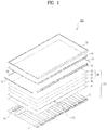
- FIG. 1 illustrates an exploded perspective view of a display device 100 in accordance with the embodiment.
- the display device 100 includes a backlight unit 110, fastening members 51 to 54, a liquid crystal panel 60, and a upper cover 70.
- the backlight unit 110 supplies a light to the liquid crystal panel 60.
- the backlight unit 110 includes a bottom cover 10, a light emission module (not shown), a reflective sheet 20, a light guide plate 30, and an optical sheet 40.
- the light emission module is provided to one side of the bottom cover 10.
- the reflective sheet 20 is disposed to a front of the bottom cover 10 in rear of the light guide plate 30 for reflecting the light from the light emission module toward the light guide plate 30 for improving optical efficiency.
- the reflective sheet 20 can be provided as a separate element as shown in FIG. 1 , or as a coating of a highly reflective material on a rear surface of the light guide plate 30 or a front surface of the bottom cover 10.
- the light guide plate 30 is disposed in front of the reflective sheet 20 for guiding the light from the light emission module to the liquid crystal panel 60.
- the optical sheet 40 is disposed on a front of the light guide plate 30 for making the light from the light guide plate 30 to diffuse and refract to improve brightness and optical efficiency.
- the optical sheet 40 can have one or a plurality of elements.
- the optical sheet 40 can have a first diffusion sheet 41, a prism sheet 42 and a second diffusion sheet 43, or one optical sheet having a function of the diffusion sheet and a function of the prism sheet.
- a number and kinds of the optical sheet 40 can be varied with a brightness characteristic.
- the diffusion sheets 41 and 43 change the light from the light guide plate 30 to a surface light source of a more uniform brightness
- the prism sheet 42 changes a side light to a frontal light and converges a radiating light to make brightness of the light higher.
- the liquid crystal panel 60 is disposed in front of the optical sheet 40, and the upper cover 70 is provided in front of the liquid crystal panel 60.
- the liquid crystal panel 60 has liquid crystals positioned between glass substrates, and polarization plates placed on the glass substrates for using polarity of the light.
- the liquid crystals have an intermediate characteristic of liquid and solid, in which the liquid crystals that are organic molecules having fluidity like liquid disposed regularly like a crystal. A picture is displayed by using a characteristic of the liquid crystals in which an orientation of liquid crystal molecules varies with external electric fields.
- the fastening members 51 to 54 are disposed between the bottom cover 10 and the upper cover 70 for fastening the bottom cover 10 and the upper cover 70, together.
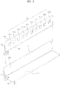
- FIG. 2 illustrates a perspective view of a light emission module 280 and a second heat sink 212 disposed on the bottom cover 10 in FIG. 1 in accordance with a preferred embodiment of the present invention.
- the bottom cover 10 can include a first forming portion 210 constructed of a metal plate having a lateral extension projected forward for reinforcing strength thereof, and second forming portions 220 formed perpendicular to the first forming portion projected forward, respectively.
- the first forming portion 210 and the second forming portion 220 can be formed by pressing the bottom cover 10 with a press.
- a first heat sink 230 in a shape of a heat sink can be mounted between adjacent second forming portions 220.
- a plurality of the first heat sinks 230 can be provided spaced from one another.
- the bottom cover 10 can have a rim wall 240 bent forward from edges thereof for preventing the reflective sheet 20, the light guide plate 30, or the optical sheet 40 from falling off to an outside of the bottom cover 10.
- an H beam can be mounted to a rear surface of the bottom cover 10.
- FIG. 2 illustrates the light emission module 280 which FIG. 1 does not show.
- the light emission module 280 is mounted to a lower portion of the bottom cover 10. Mounted between the light emission module 280 and the bottom cover 10, there is a second heat sink 212.
- the light emission module 280 is in contact with one side of the second heat sink 212, and coupled and secured thereto.
- the second heat sink 212 can be mounted to the bottom cover 10 in contact with the first heat sink 230.
- the second heat sink 212 can be mounted on an inside of the bottom cover 10 to be in contact with the rim wall 245 at one side of the bottom cover 10 and the first heat sink 230.
- the second heat sink 212 can have an "L" shaped bracket.
- the second heat sink 212 can be formed to include a first heat sink portion 212a and a second heat sink portion 212b formed as one unit.
- the first heat sink portion 212a is in surface to surface contact with the first heat sink 230, and in contact with an inside of the bottom cover 10 perpendicular to a light incident surface of the light guide plate 30.
- the second heat sink portion 212b is perpendicular to the first heat sink portion 212a and can be in surface to surface contact with the light emission module 280.
- the first heat sink portion 212a is in contact with the bottom cover 10 perpendicular to the light incident surface 120 of the light guide plate 30.
- the second heat sink portion 212b can be perpendicular to the first heat sink portion 212a and horizontal to the light incident surface 120.
- the second heat sink portion 212b can be secured to the rim wall 245 at one side of the bottom cover 10, and a rear side of the second heat sink portion 212b can be in contact with the rim wall 245 at one side of the bottom cover 10.
- the light emission module 280 includes a circuit board 282 and a light source unit 281 disposed on the circuit board 282. At least a portion of the light emission module 280 can be coupled and fastened to the second heat sink 212.
- the light source unit 281 can be an LED (Light emitting device) or an LED package, but the light source unit 281 is not limited to this.
- FIG. 3 illustrates an exploded perspective view of the light emission module 280 and the second heat sink 212 in FIG. 2 .
- the second heat sink 212 has a line of single coupling recess 310 formed in one region of the first heat sink portion 212a adjacent to the second heat sink portion 212b.
- the coupling recess 310 is in contact with the second heat sink portion 212b. That is, the line shaped coupling recess 310 is formed in the first heat sink portion 212a adjacent to a boundary surface at which the first heat sink portion 212a and the second heat sink portion 212b are in contact to each other.
- the coupling recess 310 can also be formed to open a side 320 of the first heat sink portion 212a.
- the line shaped coupling recess 310 can be horizontal to the first heat sink portion 212a.
- the light emission module 280 has the circuit board 282 and a plurality of LED packages 281:310-1 to 310-N (where N is a natural numeral greater than unity) disposed on one side of the circuit board 282 on a line.
- the circuit board 282 can be a rectangular bar.
- a side of the circuit board 282 having a relatively long length will be called as a "long side” and a side of the circuit board 282 having a relatively short length will be called as a "short side”.
- a surface having the LED packages 281 mounted thereto will be called as a "front surface" of the circuit board 282, a surface opposite thereto will be called as a "rear surface”.
- the plurality of LED packages 281 are mounted horizontal to a first long side 340 of the circuit board 282. In this instance, the plurality of LED packages 281 can be mounted adjacent to the first long side 340 closer than a second long side 350.
- Both the second long side 350 of the circuit board 282 and the coupling recess 310 can have line shapes, respectively.
- the second long side 350 of the circuit board 282 is placed in the coupling recess 310 such that a rear surface of the circuit board 282 is in contact with the second heat sink portion 212b.
- the circuit board 282 is secured to the second heat sink 212.
- a depth K1 of the coupling recess 310 can vary with a size of the circuit board 282.
- the depth K1 of the coupling recess 310 can be greater than 1/2 of a thickness m of the second heat sink portion 212b.
- a width K2 of the coupling recess 310 can be determined taking a width of the second long side 350 of the circuit board 282 into account.
- the width K2 of the coupling recess 310 can be the same with the width of the second long side 350.
- the circuit board is attached to the bottom cover or the heat sink with a two sided tape. Since the LED packages are heat sources which emit large amounts of heat, the circuit board having the LED packages mounted thereto is liable to bend by the heat from the LED packages, and since an extent of the bending is substantial, the optical characteristic of the backlight unit can become poor.
- the embodiment can reduce bending deformation of the circuit board 282 owing to a structure in which the circuit board 282 is placed in the coupling recess 310 in the second heat sink 212.
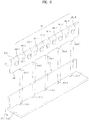
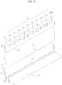
- FIG. 4 illustrates a perspective view of a light emission module and a second heat sink disposed on the bottom cover in FIG. 1 in accordance with another preferred embodiment of the present invention.
- the second heat sink 412 in FIG. 4 can be compared to the second heat sink 212 to find that the second heat sink 412 is the same with the second heat sink 212 except that a coupling recess 425 passes through the first heat sink portion 412a.
- a light emission module 280 can be secured to the second heat sink 412.
- FIG. 5 illustrates a perspective view of a light emission module 580 and a second heat sink 512 disposed on the bottom cover 10 in FIG. 1 in accordance with another preferred embodiment of the present invention
- FIG. 6 illustrates an exploded perspective view of the light emission module 580 and the second heat sink 512 in FIG. 5 .
- the light emission module 580 is in contact with one side of the second heat sink 512 and coupled and fastened thereto.
- the second heat sink 512 can be mounted to the bottom cover 10 in contact with the first heat sink 230.
- the second heat sink 512 can be "L" shaped, and can include a unitized first heat sink portion 512b and second heat sink portion 512b.
- the first heat sink portion 512a is in surface to surface contact with the first heat sink 230, and the second heat sink portion 512b can be in surface to surface contact with the light emission module 580.
- the first heat sink portion 512a and the second heat sink portion 512b can be disposed in a bent form.
- the first heat sink portion 512a is in contact with the bottom cover 10 perpendicular to the light incident surface 120 of the light guide plate 30, and a rear surface of the second heat sink portion 512b can be in contact with one side of the rim wall 245 of the bottom cover 10.
- the coupling recesses 610-1 ⁇ 610-M are spaced from one another.
- the coupling recesses 610-1 ⁇ 610-5 are in contact with the second heat sink portion 512b, and may or may not pass through the first heat sink portion 512a.
- the coupling recesses 610-1 ⁇ 610-M are formed in the first heat sink portion 512a in contact with a boundary surface of the first heat sink portion 512a and the second heat sink portion 512b.
- the light emission module 580 has a rectangular circuit board 582 and a plurality of LED packages 581:601-1 to 601-N (where N is a natural numeral greater than unity) disposed horizontal to a first long side 630 of the circuit board 282 on a line.
- a number and shapes of the coupling recesses and the coupling projections matched thereto can vary.
- the coupling projections 620-1 ⁇ 620-5 are placed in the coupling recesses matched thereto respectively such that a rear surface 650 of the circuit board 582 is in contact with the second heat sink portion 512b, and the second long side 640 of the circuit board 582 is in contact with an upper surface of the first heat sink portion 512a.
- the coupling projections 620-1 ⁇ 620-5 are placed in the coupling recesses 610-1 ⁇ 610-5 in the second heat sink 512, the circuit board 582 is fastened to the second heat sink 512.
- depths of the coupling recesses 610-1 ⁇ 610-M, lengths of the coupling projections 620-1 ⁇ 620-M, and numbers thereof can be determined.
- the depths K1 of the coupling recesses 610-1 ⁇ 610-M, the lengths of the coupling projections 620-1 ⁇ 620-M can be greater than 1/2 of a thickness m of the first heat sink portion 512a, respectively.
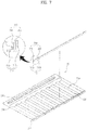
- FIG. 7 illustrates a perspective view of a light emission module and a second heat sink disposed on the bottom cover 10 in FIG. 1 in accordance with another preferred embodiment of the present invention
- FIG. 8 illustrates an exploded perspective view of the light emission module 280 and the second heat sink 712 in FIG. 7 .
- the light emission module 280 in FIG. 7 is identical to the light emission module described with reference to FIG. 3 .
- the light emission module 280 is in contact with one side of a second heat sink 712 and coupled and fastened thereto.
- the second heat sink 712 can be mounted to the bottom cover 10 in contact with the first heat sink 230.
- the second heat sink 712 can be an "L" shaped bracket, including unitized first heat sink portion 712b and second heat sink portion 712b.
- the first heat sink portion 712a is in surface to surface contact with the first heat sink 230, and the second heat sink portion 712b can be in surface to surface contact with the light emission module 280.
- first heat sink portion 712a is in contact with the bottom cover 10 perpendicular to the light incident surface 120 of the light guide plate 30, and a rear surface of the second heat sink portion 712b can be in contact with one side rim wall 245 of the bottom cover 10.
- a line shaped knoll 714 Formed on one region of the first heat sink portion 712a spaced from a distance K3 from the second heat sink portion 712b, there is a line shaped knoll 714.
- the line shaped knoll 714 is horizontal to the second heat sink portion 712b.
- the knoll 714 in FIG. 8 has one bar shape, the shape of the knoll 714 is not limited to this, but the knoll 714 can be a plurality of divided shapes spaced from each other.
- the second long side 350 is placed in a space 810 between the second heat sink portion 712b and the knoll 714 such that the rear surface of the circuit board 282 is in contact with the second heat sink portion 712b and the second long side 350 of the circuit board 282 is in contact with the first heat sink portion 712a.
- the circuit board 282 can be fastened to the second heat sink 712.
- a distance K3 of the knoll 714 from the second heat sink portion 712b is determined taking a width K2 of the second long side 350 into account. That is, the distance K3 can be the same with the width K2 of the second long side 350. And, a height D of the knoll can be determined taking secure coupling and fastening of the circuit board 282 to the second heat sink 712 into account.
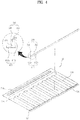
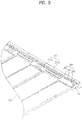
- FIG. 9 illustrates a perspective view of a light emission module 280 mounted to an inside of a bottom cover 10 of a backlight unit in accordance with a preferred embodiment of the present invention.
- the first heat sinks 230 disposed on a front side of the bottom cover 10 spaced from one another, and there is a second heat sink 212 disposed on a lower side of the first heat sink 230.
- the first heat sinks 230 is disposed in a first direction, for an example, in up/down directions, of the bottom cover 10, and the second heat sink 212 is disposed in a second direction, for an example, in a horizontal direction, of the bottom cover 10.
- the second heat sink 212 includes a first heat sink portion 212a in contact with the first heat sinks 230, and a second heat sink portion 212b perpendicular to the first heat sink portion 212a, having the light emission module 280 mounted thereon.
- the light emission module 280 is mounted to one side of the second heat sink portion 212b and includes a circuit board 282 extended along the second heat sink portion 212b, light emission devices 281 mounted on the circuit board 282 spaced from one another, and a connector 283 provided to the circuit board 282 to connect the circuit board 282 to an external power source or a printed circuit board.
- FIG. 9 illustrates a light emission device 281 of LED
- the light emission device 281 is not limited to this, but can be a lamp like CCFL, or an organic luminescence device like OLED.
- the light emission device 281 can be configured to be so called "1-edge" type in which the light emission device 281 is disposed only an upper or lower side of the display panel 60 and the bottom cover 10.
- a number of the light emission devices 281 can vary with a size of the display panel, i.e., inches of the display panel.
- the light emission device 281 can be disposed to be 2.5 ⁇ 3.5 times of the inches of the display panel.
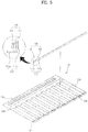
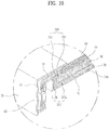
- FIG. 10 illustrates a section of the display device in FIG. 1 across a line A-A'.
- the second heat sink 212 has an "L" shape in which the first heat sink portion 212a is in contact with a lower side of the first heat sinks 230.
- the second heat sink portion 212b is formed as one unit with the first heat sink portion 212a perpendicular or an angle close to perpendicular to the first heat sink portion 212a, and the light emission module 280 is disposed to the second heat sink portion 212b, wherein the circuit board 282 is mounted to the second heat sink portion 212b, and the light emission module 280 is disposed on the circuit board 282.
- the circuit board 282 is coupled to the second heat sink 212 to be fastened thereto, in a coupling type as described with reference to FIGS. 2 to 8 .
- the coupling enables to prevent the circuit board 282 from deforming (for an example, bending) by heat from the light emission device 281.
- a reflective sheet 20 disposed in front of the second heat sink 212 and the first heat sinks 230, and there is the light guide plate 30 disposed on a front of the reflective sheet 20. Since a side (a light incident surface) of the light guide plate 30 is disposed adjacent to the light emission device 281, the light enters into the light guide plate 30 from the light emission device 281.
- a flexible circuit board 61 is connected to the liquid crystal panel 60, extends to a lower side of the backlight unit through a first fastening member 51, and is connected to a printed circuit board 62 which is disposed on a lower portion of the bottom cover 10.
- the upper cover 70 surrounds upper side, lower side, left side and right side edges of the liquid crystal panel 60 together with upper side, lower side, left side and right side edges of the backlight unit including the printed circuit board 62, the flexible printed circuit board 61, and the bottom cover 10, to couple the backlight unit and the liquid crystal panel 60, together.
- the first heat sink portion 212a can have at least one hole or recess formed therein, and the light emission module 280 can be disposed such that the light emission module 280 is inserted in and fastened to the at least one hole or recess formed in the first heat sink portion 212a in contact with the second heat sink portion 212b.
- the recess or hole in the first heat sink portion 212a can be formed in an edge of the first heat sink portion 212a adjacent to the second heat sink portion 212b.
- the recess or hole in the first heat sink portion 212a can be single recess or a plurality of recesses disposed at regular intervals.
- the recess or hole in the first heat sink portion 212a can be a single line shaped hole or a plurality of holes disposed at regular intervals.
- the knoll 714 can be constructed of one of one line shaped body formed along and in parallel to a boundary surface between the first heat sink portion 212a and the second heat sink portion 212b, or can be constructed of plural formed along and in parallel to a boundary surface between the first heat sink portion 212a and the second heat sink portion 212b at regular intervals.
- the second heat sink portion 212b can be connected to the edge region of the first heat sink portion 212a having the recess or hole formed therein and bent perpendicular to a surface of the first heat sink portion 212a.
- the light emission module 280 can have at least one coupling projection 620 at one side thereof matched to the recess or hole in the first heat sink portion 212a such that the light emission module 280 can be placed in and coupled to the recess or hole in the first heat sink portion 212a.
- the embodiment configured thus can prevent the substrate from bending by heat from the LED packages.
Description
- The present invention relates to a backlight unit and a display device therewith.
- In general, a liquid crystal display device is used widely as a monitor of a cellular phone or a computer and a display device of a television set along with a plasma display panel, or an electro-luminescence display device owing to an excellent visibility compared to a cathode ray tube CRT, low average power consumption and low heat generation compared to the same screen sized CRT.
- The liquid crystal display device is driven by utilizing optical anisotropy and polarization of liquid crystals. Since the liquid crystals are thin and lengthy, molecules of the liquid crystals can be oriented, enabling to control molecular orientation of the liquid crystals by applying an electric field to the liquid crystals, artificially.
- Therefore, if the orientation of the liquid crystal molecules is controlled as desired, the orientation of the liquid crystal molecules changes, causing a light to refract in a direction of the orientation of the liquid crystal molecules by the optical anisotropy to display picture information.
- However, since the liquid crystal display device is a light receiving device that can not emit the light spontaneously, to require a separate light source, the liquid crystal display device uses the backlight unit as a light source.
- That is, the liquid crystal display device can display a picture by directing the light from the backlight unit to an overlying liquid crystal panel and controlling a quantity of the light transmitting through the liquid crystals by varying the orientation of the liquid crystals. Document
US2009/0237957 illustrates a liquid crystal display according to the prior art. - The embodiment provides a backlight unit and a display device therewith, which can prevent a substrate thereof from bending by heat.
- Additional advantages, objects, and features of the disclosure will be set forth in part in the description which follows and in part will become apparent to those having ordinary skill in the art upon examination of the following or may be learned from practice of the invention. The objectives and other advantages of the invention may be realized and attained by the structure particularly pointed out in the written description and claims hereof as well as the appended drawings.
- To achieve these objects and other advantages and in accordance with the purpose of the invention, as embodied and broadly described herein, a backlight unit in accordance with claim 1 and a display device according with claim 12.
- In this instance, the recess in the first heat sink portion can be a line shaped single recess, or a plurality of recesses disposed at regular intervals.
- Next, the hole in the first heat sink portion can be a line shaped single hole, or a plurality of holes disposed at regular intervals.
- Then, the backlight unit can further includes a knoll formed at an edge region of the first heat sink portion adjacent to the second heat sink portion spaced from the second heat sink portion.
- In this instance, the knoll has singular which can be a line shaped one body formed along and parallel to a boundary surface between the first heat sink portion and the second heat sink portion, or plural formed along and parallel to the boundary surface between the first heat sink portion and the second heat sink portion.
- And, the second heat sink portion can be connected to the edge region of the first heat sink portion having the recess or hole formed therein and bent perpendicular to a surface of the first heat sink portion.
- Then, the light emission module can have at least one coupling projection formed at one side thereof matched to the recess or hole in the first heat sink portion.
- A backlight unit in accordance with the embodiment includes a bottom cover, a light guide plate disposed on the bottom cover, a first heat sink portion on an inside of the bottom cover to be perpendicular to a light incident surface of the light guide plate and having at least one recess formed therein, a second heat sink portion perpendicular to and being one body with the first heat sink portion, a light emission module including at least a portion of a circuit board placed in the at least one recess in the first heat sink portion, and a light source unit disposed on the circuit board, and an optical sheet disposed on the light guide plate.
- A display device having a backlight unit in accordance with the embodiment includes a bottom cover, a light guide plate disposed on the bottom cover, a first heat sink portion on an inside of the bottom cover to be perpendicular to a light incident surface of the light guide plate and having at least one recess formed therein, a second heat sink portion perpendicular to and being one body with the first heat sink portion, a light emission module including at least a portion of a circuit board placed in the at least one recess in the first heat sink portion, and a light source unit disposed on the circuit board, an optical sheet disposed on the light guide plate, and a display panel disposed on the optical sheet.
- It is to be understood that both the foregoing general description and the following detailed description of the present invention are exemplary and explanatory and are intended to provide further explanation of the invention as claimed.
- Arrangements and embodiments may be described in detail with reference to the following drawings in which like reference numerals refer to like elements and wherein:
-
FIG. 1 illustrates an exploded perspective view of a display device in accordance with the embodiment. -
FIG. 2 illustrates a perspective view of a light emission module and a second heat sink disposed on the bottom cover inFIG. 1 in accordance with a preferred embodiment of the present invention. -
FIG. 3 illustrates an exploded perspective view of the light emission module and the second heat sink inFIG. 2 . -
FIG. 4 illustrates a perspective view of a light emission module and a second heat sink disposed on the bottom cover inFIG. 1 in accordance with another preferred embodiment of the present invention. -
FIG. 5 illustrates a perspective view of a light emission module and a second heat sink disposed on the bottom cover inFIG. 1 in accordance with another preferred embodiment of the present invention. -
FIG. 6 illustrates an exploded perspective view of the light emission module and the second heat sink inFIG. 5 . -
FIG. 7 illustrates a perspective view of a light emission module and a second heat sink disposed on the bottom cover inFIG. 1 in accordance with another preferred embodiment of the present invention. -
FIG. 8 illustrates an exploded perspective view of the light emission module and the second heat sink inFIG. 7 . -
FIG. 9 illustrates a perspective view of a light emission module mounted to an inside of a bottom cover of a backlight unit in accordance with a preferred embodiment of the present invention. -
FIG. 10 illustrates a section of the display device inFIG. 1 across a line A-A'. - Reference will now be made in detail to the specific embodiments of the present invention, examples of which are illustrated in the accompanying drawings.
-
FIG. 1 illustrates an exploded perspective view of adisplay device 100 in accordance with the embodiment. Referring toFIG. 1 , thedisplay device 100 includes abacklight unit 110, fasteningmembers 51 to 54, aliquid crystal panel 60, and aupper cover 70. - The
backlight unit 110 supplies a light to theliquid crystal panel 60. Thebacklight unit 110 includes abottom cover 10, a light emission module (not shown), areflective sheet 20, alight guide plate 30, and anoptical sheet 40. - Though not shown in
FIG. 1 , the light emission module is provided to one side of thebottom cover 10. Thereflective sheet 20 is disposed to a front of thebottom cover 10 in rear of thelight guide plate 30 for reflecting the light from the light emission module toward thelight guide plate 30 for improving optical efficiency. Thereflective sheet 20 can be provided as a separate element as shown inFIG. 1 , or as a coating of a highly reflective material on a rear surface of thelight guide plate 30 or a front surface of thebottom cover 10. - The
light guide plate 30 is disposed in front of thereflective sheet 20 for guiding the light from the light emission module to theliquid crystal panel 60. - The
optical sheet 40 is disposed on a front of thelight guide plate 30 for making the light from thelight guide plate 30 to diffuse and refract to improve brightness and optical efficiency. Theoptical sheet 40 can have one or a plurality of elements. - For an example, the
optical sheet 40 can have afirst diffusion sheet 41, aprism sheet 42 and asecond diffusion sheet 43, or one optical sheet having a function of the diffusion sheet and a function of the prism sheet. A number and kinds of theoptical sheet 40 can be varied with a brightness characteristic. - In this instance, the
diffusion sheets light guide plate 30 to a surface light source of a more uniform brightness, and theprism sheet 42 changes a side light to a frontal light and converges a radiating light to make brightness of the light higher. - The
liquid crystal panel 60 is disposed in front of theoptical sheet 40, and theupper cover 70 is provided in front of theliquid crystal panel 60. Theliquid crystal panel 60 has liquid crystals positioned between glass substrates, and polarization plates placed on the glass substrates for using polarity of the light. In this instance, the liquid crystals have an intermediate characteristic of liquid and solid, in which the liquid crystals that are organic molecules having fluidity like liquid disposed regularly like a crystal. A picture is displayed by using a characteristic of the liquid crystals in which an orientation of liquid crystal molecules varies with external electric fields. - The
fastening members 51 to 54 are disposed between thebottom cover 10 and theupper cover 70 for fastening thebottom cover 10 and theupper cover 70, together. -
FIG. 2 illustrates a perspective view of alight emission module 280 and asecond heat sink 212 disposed on thebottom cover 10 inFIG. 1 in accordance with a preferred embodiment of the present invention. - Referring to
FIG. 2 , thebottom cover 10 can include a first formingportion 210 constructed of a metal plate having a lateral extension projected forward for reinforcing strength thereof, and second formingportions 220 formed perpendicular to the first forming portion projected forward, respectively. The first formingportion 210 and the second formingportion 220 can be formed by pressing thebottom cover 10 with a press. - Between adjacent
second forming portions 220, afirst heat sink 230 in a shape of a heat sink can be mounted. A plurality of thefirst heat sinks 230 can be provided spaced from one another. - The
bottom cover 10 can have arim wall 240 bent forward from edges thereof for preventing thereflective sheet 20, thelight guide plate 30, or theoptical sheet 40 from falling off to an outside of thebottom cover 10. In order to reinforce thebottom cover 10, an H beam can be mounted to a rear surface of thebottom cover 10. -
FIG. 2 illustrates thelight emission module 280 whichFIG. 1 does not show. Thelight emission module 280 is mounted to a lower portion of thebottom cover 10. Mounted between thelight emission module 280 and thebottom cover 10, there is asecond heat sink 212. - The
light emission module 280 is in contact with one side of thesecond heat sink 212, and coupled and secured thereto. Thesecond heat sink 212 can be mounted to thebottom cover 10 in contact with thefirst heat sink 230. - In detail, the
second heat sink 212 can be mounted on an inside of thebottom cover 10 to be in contact with therim wall 245 at one side of thebottom cover 10 and thefirst heat sink 230. - For an example, the
second heat sink 212 can have an "L" shaped bracket. In this instance, thesecond heat sink 212 can be formed to include a firstheat sink portion 212a and a secondheat sink portion 212b formed as one unit. - The first
heat sink portion 212a is in surface to surface contact with thefirst heat sink 230, and in contact with an inside of thebottom cover 10 perpendicular to a light incident surface of thelight guide plate 30. The secondheat sink portion 212b is perpendicular to the firstheat sink portion 212a and can be in surface to surface contact with thelight emission module 280. - In detail, the first
heat sink portion 212a is in contact with thebottom cover 10 perpendicular to thelight incident surface 120 of thelight guide plate 30. The secondheat sink portion 212b can be perpendicular to the firstheat sink portion 212a and horizontal to thelight incident surface 120. The secondheat sink portion 212b can be secured to therim wall 245 at one side of thebottom cover 10, and a rear side of the secondheat sink portion 212b can be in contact with therim wall 245 at one side of thebottom cover 10. - The
light emission module 280 includes acircuit board 282 and alight source unit 281 disposed on thecircuit board 282. At least a portion of thelight emission module 280 can be coupled and fastened to thesecond heat sink 212. Thelight source unit 281 can be an LED (Light emitting device) or an LED package, but thelight source unit 281 is not limited to this. -
FIG. 3 illustrates an exploded perspective view of thelight emission module 280 and thesecond heat sink 212 inFIG. 2 . - Referring to
FIG. 3 , thesecond heat sink 212 has a line ofsingle coupling recess 310 formed in one region of the firstheat sink portion 212a adjacent to the secondheat sink portion 212b. Thecoupling recess 310 is in contact with the secondheat sink portion 212b. That is, the line shapedcoupling recess 310 is formed in the firstheat sink portion 212a adjacent to a boundary surface at which the firstheat sink portion 212a and the secondheat sink portion 212b are in contact to each other. Thecoupling recess 310 can also be formed to open aside 320 of the firstheat sink portion 212a. The line shapedcoupling recess 310 can be horizontal to the firstheat sink portion 212a. - The
light emission module 280 has thecircuit board 282 and a plurality of LED packages 281:310-1 to 310-N (where N is a natural numeral greater than unity) disposed on one side of thecircuit board 282 on a line. Thecircuit board 282 can be a rectangular bar. A side of thecircuit board 282 having a relatively long length will be called as a "long side" and a side of thecircuit board 282 having a relatively short length will be called as a "short side". And, a surface having the LED packages 281 mounted thereto will be called as a "front surface" of thecircuit board 282, a surface opposite thereto will be called as a "rear surface". - The plurality of
LED packages 281 are mounted horizontal to a firstlong side 340 of thecircuit board 282. In this instance, the plurality ofLED packages 281 can be mounted adjacent to the firstlong side 340 closer than a secondlong side 350. - Both the second
long side 350 of thecircuit board 282 and thecoupling recess 310 can have line shapes, respectively. The secondlong side 350 of thecircuit board 282 is placed in thecoupling recess 310 such that a rear surface of thecircuit board 282 is in contact with the secondheat sink portion 212b. As the secondlong side 350 is placed in thecoupling recess 310 in thesecond heat sink 212, thecircuit board 282 is secured to thesecond heat sink 212. - A depth K1 of the
coupling recess 310 can vary with a size of thecircuit board 282. For an example, in order to make the secondlong side 350 of thecircuit board 282 to couple to thecoupling recess 310 for fastening thecircuit board 282 to thesecond heat sink 212 securely, the depth K1 of thecoupling recess 310 can be greater than 1/2 of a thickness m of the secondheat sink portion 212b. - And, in order to make the second
long side 350 of thecircuit board 282 to couple and fasten to thecoupling recess 310 securely, a width K2 of thecoupling recess 310 can be determined taking a width of the secondlong side 350 of thecircuit board 282 into account. For an example, the width K2 of thecoupling recess 310 can be the same with the width of the secondlong side 350. - In the related art backlight unit, the circuit board is attached to the bottom cover or the heat sink with a two sided tape. Since the LED packages are heat sources which emit large amounts of heat, the circuit board having the LED packages mounted thereto is liable to bend by the heat from the LED packages, and since an extent of the bending is substantial, the optical characteristic of the backlight unit can become poor.
- Even if a tensile force caused by the heat from the LED packages 330-1 to 330-N acts on the
circuit board 282, the embodiment can reduce bending deformation of thecircuit board 282 owing to a structure in which thecircuit board 282 is placed in thecoupling recess 310 in thesecond heat sink 212. -
FIG. 4 illustrates a perspective view of a light emission module and a second heat sink disposed on the bottom cover inFIG. 1 in accordance with another preferred embodiment of the present invention. Thesecond heat sink 412 inFIG. 4 can be compared to thesecond heat sink 212 to find that thesecond heat sink 412 is the same with thesecond heat sink 212 except that acoupling recess 425 passes through the firstheat sink portion 412a. As a secondlong side 350 of thecircuit board 282 is placed in thecoupling recess 425, alight emission module 280 can be secured to thesecond heat sink 412. -
FIG. 5 illustrates a perspective view of alight emission module 580 and asecond heat sink 512 disposed on thebottom cover 10 inFIG. 1 in accordance with another preferred embodiment of the present invention, andFIG. 6 illustrates an exploded perspective view of thelight emission module 580 and thesecond heat sink 512 inFIG. 5 . - Referring to
FIG. 5 , thelight emission module 580 is in contact with one side of thesecond heat sink 512 and coupled and fastened thereto. Thesecond heat sink 512 can be mounted to thebottom cover 10 in contact with thefirst heat sink 230. - The
second heat sink 512 can be "L" shaped, and can include a unitized firstheat sink portion 512b and secondheat sink portion 512b. - The first
heat sink portion 512a is in surface to surface contact with thefirst heat sink 230, and the secondheat sink portion 512b can be in surface to surface contact with thelight emission module 580. The firstheat sink portion 512a and the secondheat sink portion 512b can be disposed in a bent form. - In detail, the first
heat sink portion 512a is in contact with thebottom cover 10 perpendicular to thelight incident surface 120 of thelight guide plate 30, and a rear surface of the secondheat sink portion 512b can be in contact with one side of therim wall 245 of thebottom cover 10. - Formed in one region of the first
heat sink portion 512a adjacent to the secondheat sink portion 512b, there are a plurality of coupling recesses 610-1 ∼ 610-M (for an example, M=5) spaced from one another. In this instance, the coupling recesses 610-1 ∼ 610-5 are in contact with the secondheat sink portion 512b, and may or may not pass through the firstheat sink portion 512a. - That is, the coupling recesses 610-1 ∼ 610-M are formed in the first
heat sink portion 512a in contact with a boundary surface of the firstheat sink portion 512a and the secondheat sink portion 512b. - The
light emission module 580 has arectangular circuit board 582 and a plurality of LED packages 581:601-1 to 601-N (where N is a natural numeral greater than unity) disposed horizontal to a firstlong side 630 of thecircuit board 282 on a line. - The
circuit board 582 has coupling projections 620-1 ∼ 620-M (for an example, M=5) formed in thelong side 640 to match with the coupling recesses 610-1 ∼ 610-5 in the firstheat sink portion 512a. In this instance, a number and shapes of the coupling recesses and the coupling projections matched thereto can vary. - The coupling projections 620-1 ∼ 620-5 are placed in the coupling recesses matched thereto respectively such that a rear surface 650 of the
circuit board 582 is in contact with the secondheat sink portion 512b, and the secondlong side 640 of thecircuit board 582 is in contact with an upper surface of the firstheat sink portion 512a. As the coupling projections 620-1 ∼ 620-5 are placed in the coupling recesses 610-1 ∼ 610-5 in thesecond heat sink 512, thecircuit board 582 is fastened to thesecond heat sink 512. - In order to make the
circuit board 582 to be coupled and fastened to thesecond heat sink 512 securely, depths of the coupling recesses 610-1 ∼ 610-M, lengths of the coupling projections 620-1 ∼ 620-M, and numbers thereof can be determined. For an example, the depths K1 of the coupling recesses 610-1 ∼ 610-M, the lengths of the coupling projections 620-1 ∼ 620-M can be greater than 1/2 of a thickness m of the firstheat sink portion 512a, respectively. -
FIG. 7 illustrates a perspective view of a light emission module and a second heat sink disposed on thebottom cover 10 inFIG. 1 in accordance with another preferred embodiment of the present invention, andFIG. 8 illustrates an exploded perspective view of thelight emission module 280 and thesecond heat sink 712 inFIG. 7 . Thelight emission module 280 inFIG. 7 is identical to the light emission module described with reference toFIG. 3 . - Referring to
FIGS. 7 and8 , thelight emission module 280 is in contact with one side of asecond heat sink 712 and coupled and fastened thereto. Thesecond heat sink 712 can be mounted to thebottom cover 10 in contact with thefirst heat sink 230. - The
second heat sink 712 can be an "L" shaped bracket, including unitized firstheat sink portion 712b and secondheat sink portion 712b. - The first
heat sink portion 712a is in surface to surface contact with thefirst heat sink 230, and the secondheat sink portion 712b can be in surface to surface contact with thelight emission module 280. - In detail, the first
heat sink portion 712a is in contact with thebottom cover 10 perpendicular to thelight incident surface 120 of thelight guide plate 30, and a rear surface of the secondheat sink portion 712b can be in contact with oneside rim wall 245 of thebottom cover 10. - Formed on one region of the first
heat sink portion 712a spaced from a distance K3 from the secondheat sink portion 712b, there is a line shapedknoll 714. The line shapedknoll 714 is horizontal to the secondheat sink portion 712b. Though theknoll 714 inFIG. 8 has one bar shape, the shape of theknoll 714 is not limited to this, but theknoll 714 can be a plurality of divided shapes spaced from each other. - The second
long side 350 is placed in aspace 810 between the secondheat sink portion 712b and theknoll 714 such that the rear surface of thecircuit board 282 is in contact with the secondheat sink portion 712b and the secondlong side 350 of thecircuit board 282 is in contact with the firstheat sink portion 712a. As the secondlong side 350 is placed in thespace 810 between the secondheat sink portion 712b and theknoll 714, thecircuit board 282 can be fastened to thesecond heat sink 712. - A distance K3 of the
knoll 714 from the secondheat sink portion 712b is determined taking a width K2 of the secondlong side 350 into account. That is, the distance K3 can be the same with the width K2 of the secondlong side 350. And, a height D of the knoll can be determined taking secure coupling and fastening of thecircuit board 282 to thesecond heat sink 712 into account. -
FIG. 9 illustrates a perspective view of alight emission module 280 mounted to an inside of abottom cover 10 of a backlight unit in accordance with a preferred embodiment of the present invention. As shown inFIG. 9 , there are thefirst heat sinks 230 disposed on a front side of thebottom cover 10 spaced from one another, and there is asecond heat sink 212 disposed on a lower side of thefirst heat sink 230. - The
first heat sinks 230 is disposed in a first direction, for an example, in up/down directions, of thebottom cover 10, and thesecond heat sink 212 is disposed in a second direction, for an example, in a horizontal direction, of thebottom cover 10. - The
second heat sink 212 includes a firstheat sink portion 212a in contact with thefirst heat sinks 230, and a secondheat sink portion 212b perpendicular to the firstheat sink portion 212a, having thelight emission module 280 mounted thereon. - The
light emission module 280 is mounted to one side of the secondheat sink portion 212b and includes acircuit board 282 extended along the secondheat sink portion 212b,light emission devices 281 mounted on thecircuit board 282 spaced from one another, and aconnector 283 provided to thecircuit board 282 to connect thecircuit board 282 to an external power source or a printed circuit board. - Though
FIG. 9 illustrates alight emission device 281 of LED, thelight emission device 281 is not limited to this, but can be a lamp like CCFL, or an organic luminescence device like OLED. Thelight emission device 281 can be configured to be so called "1-edge" type in which thelight emission device 281 is disposed only an upper or lower side of thedisplay panel 60 and thebottom cover 10. - A number of the
light emission devices 281 can vary with a size of the display panel, i.e., inches of the display panel. Thelight emission device 281 can be disposed to be 2.5 ∼ 3.5 times of the inches of the display panel. -
FIG. 10 illustrates a section of the display device inFIG. 1 across a line A-A'. As shown inFIG. 10 , thesecond heat sink 212 has an "L" shape in which the firstheat sink portion 212a is in contact with a lower side of the first heat sinks 230. - The second
heat sink portion 212b is formed as one unit with the firstheat sink portion 212a perpendicular or an angle close to perpendicular to the firstheat sink portion 212a, and thelight emission module 280 is disposed to the secondheat sink portion 212b, wherein thecircuit board 282 is mounted to the secondheat sink portion 212b, and thelight emission module 280 is disposed on thecircuit board 282. - The
circuit board 282 is coupled to thesecond heat sink 212 to be fastened thereto, in a coupling type as described with reference toFIGS. 2 to 8 . The coupling enables to prevent thecircuit board 282 from deforming (for an example, bending) by heat from thelight emission device 281. - In a case power is applied to the
circuit board 282 for thelight emission device 281 to emit a light, the heat is generated consequently, transmitted to thefirst heat sinks 230 which is in contact with thesecond heat sink 212 via thesecond heat sink 212, and dissipated therefrom to an outside of the backlight unit. - There is a
reflective sheet 20 disposed in front of thesecond heat sink 212 and thefirst heat sinks 230, and there is thelight guide plate 30 disposed on a front of thereflective sheet 20. Since a side (a light incident surface) of thelight guide plate 30 is disposed adjacent to thelight emission device 281, the light enters into thelight guide plate 30 from thelight emission device 281. - Most of the light entered into the
light guide plate 30 thus is directed forward while being reflected, totally reflected, and refracted within the light guide plate. However, the light travels backward is reflected at thereflective sheet 20 to return into thelight guide plate 30, again. - Provided on a front of the
light guide plate 30, there is anoptical sheet 40 for causing an optical phenomenon of the light, and disposed in front of theoptical sheet 40, there is adisplay panel 60. Aflexible circuit board 61 is connected to theliquid crystal panel 60, extends to a lower side of the backlight unit through afirst fastening member 51, and is connected to a printedcircuit board 62 which is disposed on a lower portion of thebottom cover 10. - The
upper cover 70 surrounds upper side, lower side, left side and right side edges of theliquid crystal panel 60 together with upper side, lower side, left side and right side edges of the backlight unit including the printedcircuit board 62, the flexible printedcircuit board 61, and thebottom cover 10, to couple the backlight unit and theliquid crystal panel 60, together. - In the embodiment configured thus, the first
heat sink portion 212a can have at least one hole or recess formed therein, and thelight emission module 280 can be disposed such that thelight emission module 280 is inserted in and fastened to the at least one hole or recess formed in the firstheat sink portion 212a in contact with the secondheat sink portion 212b. - The recess or hole in the first
heat sink portion 212a can be formed in an edge of the firstheat sink portion 212a adjacent to the secondheat sink portion 212b. - In this instance, the recess or hole in the first
heat sink portion 212a can be single recess or a plurality of recesses disposed at regular intervals. - Or, the recess or hole in the first
heat sink portion 212a can be a single line shaped hole or a plurality of holes disposed at regular intervals. - There can be at least one
knoll 714 formed at an edge region of the firstheat sink portion 212a adjacent to the secondheat sink portion 212b spaced from the secondheat sink portion 212b. - In this instance, the
knoll 714 can be constructed of one of one line shaped body formed along and in parallel to a boundary surface between the firstheat sink portion 212a and the secondheat sink portion 212b, or can be constructed of plural formed along and in parallel to a boundary surface between the firstheat sink portion 212a and the secondheat sink portion 212b at regular intervals. - And, the second
heat sink portion 212b can be connected to the edge region of the firstheat sink portion 212a having the recess or hole formed therein and bent perpendicular to a surface of the firstheat sink portion 212a. - And, the
light emission module 280 can have at least one coupling projection 620 at one side thereof matched to the recess or hole in the firstheat sink portion 212a such that thelight emission module 280 can be placed in and coupled to the recess or hole in the firstheat sink portion 212a. - The embodiment configured thus can prevent the substrate from bending by heat from the LED packages.
- Although embodiments have been described with reference to a number of illustrative embodiments thereof, it should be understood that numerous other modifications and embodiments can be devised by those skilled in the art that will fall within the spirit and scope of the principles of this disclosure. More particularly, various variations and modifications are possible in the component parts and/or arrangements of the subject combination arrangement within the scope of the disclosure, the drawings and the appended claims. In addition to variations and modifications in the component parts and/or arrangements, alternative uses will also be apparent to those skilled in the art.
Claims (16)
- A backlight unit comprising:a bottom cover (10) including a first heat sink (230) in a shape of a heat sink;a second heat sink (212) having an L-shaped bracket mounted to the bottom cover (10) and including a first heat sink portion (212a) being in surface to surface contact with the first heat sink (210) and a second heat sink portion (212b) extended upward with respect to the first heat sink portion (212a) andat least a portion of a light emission module (280) placed in at least one recess (310) or at least one hole (610) of the first heat sink portion (212a) and the light emission module (280) disposed on the second heat sink portion (212b).
- The backlight unit as claimed in claim 1, wherein the recess or hole in the first heat sink portion is formed in an edge of the first heat sink portion adjacent to the second heat sink portion.
- The backlight unit as claimed in claim 1, wherein the recess or hole in the first heat sink portion is a line shaped single recess or hole.
- The backlight unit as claimed in claim 1, wherein the recess or hole in the first heat sink portion is a plurality of recesses or holes disposed at regular intervals.
- The backlight unit as claimed in claim 1, wherein the bottom cover comprises:a first forming portion constructed of a metal plate having a lateral extension projected forward for reinforcing strength thereof; andplural second forming portions formed perpendicular to the first forming portion projected forward, respectively.
- The backlight unit as claimed in claim 1, wherein the bottom cover further comprises a rim wall bent forward from edges thereof.
- The backlight unit as claimed in claim 1, wherein the second heat sink portion is connected to the edge region of the first heat sink portion having the recess or hole formed therein and bent perpendicular to a surface of the first heat sink portion.
- The backlight unit as claimed in claim 1, wherein the light emission module has at least one coupling projection formed at one side thereof matched to the recess or hole in the first heat sink portion.
- The backlight unit as claimed in claim 1, further comprising:a reflective sheet arranged on the bottom cover;a light guide plate arranged on the reflective sheet; andan optical sheet arranged on the light guide plate,wherein the first heat sink portion is on an inside of the bottom cover to be perpendicular to a light incident surface of the light guide plate and having at least one recess,the second heat sink portion is perpendicular to and is one body with the first heat sink portion, andthe light emission module includes at least a portion of a circuit board placed in the at least one recess in the first heat sink portion, and a light source unit arranged on the circuit board.
- The backlight unit as claimed in claim 9, wherein the circuit board has a long side placed in the at least one recess such that a rear surface of the circuit board is on the second heat sink portion.
- The backlight unit as claimed in claim 9, wherein the at least one recess is formed to open a side of the first heat sink portion.
- A display device having a backlight unit, the display device comprising:a bottom cover including a first heat sink; a light guide plate disposed on the bottom cover; a second heat sink having an L-shaped bracket mounted to the bottom cover, including a first heat sink portion being in surface to surface contact with the first heat sink to be perpendicular to a light incident surface of the light guide plate, a second heat sink portion perpendicular to and being one body with the first heat sink portion, and a knoll formed at an edge region of the first heat sink portion adjacent to the second heat sink portion spaced from the second heat sink portion;a light emission module including at least a portion of a circuit board placed in the at least one recess in the first heat sink portion, and a light source unit disposed on the circuit board;an optical sheet disposed on the light guide plate; anda display panel disposed on the optical sheet.
- The display device as claimed in claim 12, wherein the knoll has singular which is a line shaped one body formed along and parallel to a boundary surface between the first heat sink portion and the second heat sink portion.
- The display device as claimed in claim 12, wherein the knoll has plural formed along and parallel to the boundary surface between the first heat sink portion and the second heat sink portion.
- The display device as claimed in claim 12, further comprising a reflective sheet arranged between the bottom cover and the light guide plate.
- The display device as claimed in claim 12, wherein the bottom cover comprises:a first forming constructed of a metal plate having a lateral extension projected forward for reinforcing strength thereof.
Applications Claiming Priority (1)
| Application Number | Priority Date | Filing Date | Title |
|---|---|---|---|
| KR1020100066206A KR101729264B1 (en) | 2010-07-09 | 2010-07-09 | A backlight unit and a display device |
Publications (3)
| Publication Number | Publication Date |
|---|---|
| EP2405188A2 EP2405188A2 (en) | 2012-01-11 |
| EP2405188A3 EP2405188A3 (en) | 2014-12-24 |
| EP2405188B1 true EP2405188B1 (en) | 2018-01-03 |
Family
ID=44786943
Family Applications (1)
| Application Number | Title | Priority Date | Filing Date |
|---|---|---|---|
| EP11170066.2A Active EP2405188B1 (en) | 2010-07-09 | 2011-06-15 | Backlight unit and display device therewith |
Country Status (5)
| Country | Link |
|---|---|
| US (1) | US8616752B2 (en) |
| EP (1) | EP2405188B1 (en) |
| JP (1) | JP5973138B2 (en) |
| KR (1) | KR101729264B1 (en) |
| CN (1) | CN102338327B (en) |
Families Citing this family (9)
| Publication number | Priority date | Publication date | Assignee | Title |
|---|---|---|---|---|
| JP5021102B1 (en) * | 2011-09-30 | 2012-09-05 | シャープ株式会社 | Liquid crystal display |
| WO2013094975A1 (en) * | 2011-12-23 | 2013-06-27 | Samsung Electronics Co., Ltd. | Display module and display apparatus having the same |
| CN104081113A (en) * | 2012-02-17 | 2014-10-01 | 夏普株式会社 | Illumination device, display device and television receiver |
| KR101259347B1 (en) * | 2012-06-05 | 2013-04-30 | 주식회사 파인디앤씨 | Stand frame of led for backlight unit |
| JP2014085653A (en) * | 2012-10-26 | 2014-05-12 | Funai Electric Co Ltd | Display device |
| JP2014086406A (en) * | 2012-10-26 | 2014-05-12 | Funai Electric Co Ltd | Display device |
| KR101990528B1 (en) * | 2012-11-08 | 2019-06-18 | 엘지디스플레이 주식회사 | LED assembly and liquid crystal display device using the same |
| JP2014170079A (en) * | 2013-03-01 | 2014-09-18 | Funai Electric Co Ltd | Display device |
| KR102306022B1 (en) | 2014-12-31 | 2021-09-30 | 엘지전자 주식회사 | Back light unit and display apparatus having it |
Citations (1)
| Publication number | Priority date | Publication date | Assignee | Title |
|---|---|---|---|---|
| US20090237957A1 (en) * | 2008-03-19 | 2009-09-24 | Epson Imaging Devices Corporation | Illumination device, method of assembling illumination device, and liquid crystal display device |
Family Cites Families (25)
| Publication number | Priority date | Publication date | Assignee | Title |
|---|---|---|---|---|
| JP3135971B2 (en) * | 1992-02-25 | 2001-02-19 | 松下電工株式会社 | Electronic time switch |
| KR100541277B1 (en) | 1998-08-26 | 2006-03-14 | 삼성전자주식회사 | Backlight Assembly of Liquid Crystal Display |
| JP2003279973A (en) | 2002-03-20 | 2003-10-02 | Kawaguchiko Seimitsu Co Ltd | Backlight attaching structure for liquid crystal display device |
| KR100959785B1 (en) * | 2003-09-16 | 2010-05-28 | 삼성전자주식회사 | Back light assembly and liquid crystal display device having the same |
| JP2005267852A (en) * | 2004-03-16 | 2005-09-29 | Sharp Corp | Backlight reflecting plate |
| JP2006208723A (en) | 2005-01-27 | 2006-08-10 | Minebea Co Ltd | Liquid crystal display device |
| TWI339760B (en) * | 2005-05-30 | 2011-04-01 | Kyocera Corp | Backlight device and liquid crystal display device |
| JP2007163620A (en) | 2005-12-12 | 2007-06-28 | Hitachi Displays Ltd | Liquid crystal display device and backlight device |
| JP4654920B2 (en) * | 2006-01-19 | 2011-03-23 | 三菱電機株式会社 | Light source device and liquid crystal display device |
| CN101004515A (en) * | 2006-01-21 | 2007-07-25 | 鸿富锦精密工业(深圳)有限公司 | Full run-down type backlight module |
| KR100978045B1 (en) * | 2006-03-13 | 2010-08-26 | 삼성전자주식회사 | Lyquid crystal panel assembly and lyquid crystal display having the same |
| JP4840121B2 (en) * | 2006-04-20 | 2011-12-21 | 三菱電機株式会社 | Surface light source device |
| TW200811522A (en) * | 2006-08-22 | 2008-03-01 | Chunghwa Picture Tubes Ltd | Light-source fixing structure for backlight module |
| CN101131500A (en) | 2006-08-23 | 2008-02-27 | 中华映管股份有限公司 | Light source fixing structure of backlight component |
| JP4915911B2 (en) * | 2006-10-02 | 2012-04-11 | 株式会社 日立ディスプレイズ | Liquid crystal display |
| US8147113B2 (en) * | 2007-01-22 | 2012-04-03 | Sharp Kabushiki Kaisha | Backlight device and flat display using it |
| TWM324216U (en) * | 2007-05-23 | 2007-12-21 | Everlight Electronics Co Ltd | LED back light module |
| KR100879772B1 (en) | 2007-09-06 | 2009-01-21 | 한성엘컴텍 주식회사 | Surface emission device having a plurality of light emission devices |
| JP5073808B2 (en) | 2008-02-28 | 2012-11-14 | シャープ株式会社 | Backlight unit and liquid crystal display device |
| KR101322312B1 (en) | 2008-05-23 | 2013-10-25 | 엘지디스플레이 주식회사 | Liquid crystal display device |
| CN101338867B (en) | 2008-09-01 | 2012-09-05 | 友达光电股份有限公司 | Backlight module and LCD device |
| KR101529579B1 (en) * | 2008-11-13 | 2015-06-19 | 삼성디스플레이 주식회사 | Back-light assembly, display device having the same and method of manufacturing display device |
| JP2010147012A (en) * | 2008-12-22 | 2010-07-01 | Panasonic Electric Works Co Ltd | Planar light source, and display lighting fixture |
| KR101529556B1 (en) * | 2008-12-26 | 2015-06-17 | 엘지디스플레이 주식회사 | Liquid crystal display device having good heat radiating function |
| KR20100106790A (en) * | 2009-03-24 | 2010-10-04 | 삼성전자주식회사 | Display device |
-
2010
- 2010-07-09 KR KR1020100066206A patent/KR101729264B1/en active IP Right Grant
-
2011
- 2011-06-15 EP EP11170066.2A patent/EP2405188B1/en active Active
- 2011-06-30 US US13/174,037 patent/US8616752B2/en active Active
- 2011-06-30 CN CN201110186421.4A patent/CN102338327B/en active Active
- 2011-07-08 JP JP2011151730A patent/JP5973138B2/en not_active Expired - Fee Related
Patent Citations (1)
| Publication number | Priority date | Publication date | Assignee | Title |
|---|---|---|---|---|
| US20090237957A1 (en) * | 2008-03-19 | 2009-09-24 | Epson Imaging Devices Corporation | Illumination device, method of assembling illumination device, and liquid crystal display device |
Also Published As
| Publication number | Publication date |
|---|---|
| JP5973138B2 (en) | 2016-08-23 |
| JP2012018927A (en) | 2012-01-26 |
| KR20120005657A (en) | 2012-01-17 |
| US20120008337A1 (en) | 2012-01-12 |
| EP2405188A3 (en) | 2014-12-24 |
| EP2405188A2 (en) | 2012-01-11 |
| KR101729264B1 (en) | 2017-05-02 |
| US8616752B2 (en) | 2013-12-31 |
| CN102338327A (en) | 2012-02-01 |
| CN102338327B (en) | 2014-03-12 |
Similar Documents
| Publication | Publication Date | Title |
|---|---|---|
| EP2405188B1 (en) | Backlight unit and display device therewith | |
| EP2390712B1 (en) | Backlight unit and display device including the same | |
| US7156548B2 (en) | Light guide plate with v-shaped grooves and backlight module incorporating same | |
| US9715139B2 (en) | Curved display device | |
| US8439551B2 (en) | Backlight assembly and display device having the same | |
| US20050281052A1 (en) | Light guide plate having V-cut grooves and a liquid crystal display using the same | |
| US8462291B2 (en) | Backlight module with film positioning function and display device using the same | |
| US9261721B2 (en) | Display apparatus | |
| EP2219054A1 (en) | Light emitting module and display device having the same | |
| EP2530375B1 (en) | Light guide design for edge-illumination in a backlight unit | |
| US10281765B2 (en) | Backlight unit provided with supporter of light source unit, manufacturing method of the supporter, and display device including the backlight unit | |
| KR101338020B1 (en) | Liquid crystal display device | |
| KR101975488B1 (en) | Backlight assembly and display device comprising the same | |
| EP2728401A1 (en) | Display module and display apparatus having the same | |
| US20140104873A1 (en) | Backlight module | |
| US20060146227A1 (en) | Prism sheet and liquid crystal display apparatus using thereof | |
| KR102128797B1 (en) | Light reflector, back light unit having the same, and display device having thereof | |
| US20140119056A1 (en) | Light Guide Plate and Backlight Module Using the Light Guide Plate | |
| US10514153B2 (en) | Backlight module and display device | |
| KR101712096B1 (en) | A backlight unit and a display device | |
| US8752993B2 (en) | Backlight module with optic film assembly mounted through snap fitting | |
| KR102049985B1 (en) | Back light unit and display device comprising the same | |
| EP3333621B1 (en) | Display apparatus | |
| EP2372418A2 (en) | Backlight unit and display apparatus | |
| CN213457599U (en) | Backlight module, display device and electronic product |
Legal Events
| Date | Code | Title | Description |
|---|---|---|---|
| 17P | Request for examination filed |
Effective date: 20110615 |
|
| AK | Designated contracting states |
Kind code of ref document: A2 Designated state(s): AL AT BE BG CH CY CZ DE DK EE ES FI FR GB GR HR HU IE IS IT LI LT LU LV MC MK MT NL NO PL PT RO RS SE SI SK SM TR |
|
| AX | Request for extension of the european patent |
Extension state: BA ME |
|
| PUAI | Public reference made under article 153(3) epc to a published international application that has entered the european phase |
Free format text: ORIGINAL CODE: 0009012 |
|
| RAP1 | Party data changed (applicant data changed or rights of an application transferred) |
Owner name: LG INNOTEK CO., LTD. |
|
| PUAL | Search report despatched |
Free format text: ORIGINAL CODE: 0009013 |
|
| AK | Designated contracting states |
Kind code of ref document: A3 Designated state(s): AL AT BE BG CH CY CZ DE DK EE ES FI FR GB GR HR HU IE IS IT LI LT LU LV MC MK MT NL NO PL PT RO RS SE SI SK SM TR |
|
| AX | Request for extension of the european patent |
Extension state: BA ME |
|
| RIC1 | Information provided on ipc code assigned before grant |
Ipc: G02B 6/00 20060101ALI20141118BHEP Ipc: F21V 8/00 20060101AFI20141118BHEP |
|
| RBV | Designated contracting states (corrected) |
Designated state(s): AL AT BE BG CH CY CZ DE DK EE ES FI FR GB GR HR HU IE IS IT LI LT LU LV MC MK MT NL NO PL PT RO RS SE SI SK SM TR |
|
| 17Q | First examination report despatched |
Effective date: 20160609 |
|
| RAP1 | Party data changed (applicant data changed or rights of an application transferred) |
Owner name: LG INNOTEK CO., LTD. |
|
| GRAP | Despatch of communication of intention to grant a patent |
Free format text: ORIGINAL CODE: EPIDOSNIGR1 |
|
| INTG | Intention to grant announced |
Effective date: 20170712 |
|
| GRAS | Grant fee paid |
Free format text: ORIGINAL CODE: EPIDOSNIGR3 |
|
| GRAA | (expected) grant |
Free format text: ORIGINAL CODE: 0009210 |
|
| AK | Designated contracting states |
Kind code of ref document: B1 Designated state(s): AL AT BE BG CH CY CZ DE DK EE ES FI FR GB GR HR HU IE IS IT LI LT LU LV MC MK MT NL NO PL PT RO RS SE SI SK SM TR |
|
| REG | Reference to a national code |
Ref country code: GB Ref legal event code: FG4D |
|
| REG | Reference to a national code |
Ref country code: CH Ref legal event code: EP Ref country code: AT Ref legal event code: REF Ref document number: 960627 Country of ref document: AT Kind code of ref document: T Effective date: 20180115 |
|
| REG | Reference to a national code |
Ref country code: IE Ref legal event code: FG4D |
|
| REG | Reference to a national code |
Ref country code: DE Ref legal event code: R096 Ref document number: 602011044660 Country of ref document: DE |
|
| REG | Reference to a national code |
Ref country code: NL Ref legal event code: MP Effective date: 20180103 Ref country code: FR Ref legal event code: PLFP Year of fee payment: 8 |
|
| REG | Reference to a national code |
Ref country code: LT Ref legal event code: MG4D |
|
| REG | Reference to a national code |
Ref country code: AT Ref legal event code: MK05 Ref document number: 960627 Country of ref document: AT Kind code of ref document: T Effective date: 20180103 |
|
| PG25 | Lapsed in a contracting state [announced via postgrant information from national office to epo] |
Ref country code: NL Free format text: LAPSE BECAUSE OF FAILURE TO SUBMIT A TRANSLATION OF THE DESCRIPTION OR TO PAY THE FEE WITHIN THE PRESCRIBED TIME-LIMIT Effective date: 20180103 |
|
| PG25 | Lapsed in a contracting state [announced via postgrant information from national office to epo] |
Ref country code: FI Free format text: LAPSE BECAUSE OF FAILURE TO SUBMIT A TRANSLATION OF THE DESCRIPTION OR TO PAY THE FEE WITHIN THE PRESCRIBED TIME-LIMIT Effective date: 20180103 Ref country code: NO Free format text: LAPSE BECAUSE OF FAILURE TO SUBMIT A TRANSLATION OF THE DESCRIPTION OR TO PAY THE FEE WITHIN THE PRESCRIBED TIME-LIMIT Effective date: 20180403 Ref country code: CY Free format text: LAPSE BECAUSE OF FAILURE TO SUBMIT A TRANSLATION OF THE DESCRIPTION OR TO PAY THE FEE WITHIN THE PRESCRIBED TIME-LIMIT Effective date: 20180103 Ref country code: LT Free format text: LAPSE BECAUSE OF FAILURE TO SUBMIT A TRANSLATION OF THE DESCRIPTION OR TO PAY THE FEE WITHIN THE PRESCRIBED TIME-LIMIT Effective date: 20180103 Ref country code: HR Free format text: LAPSE BECAUSE OF FAILURE TO SUBMIT A TRANSLATION OF THE DESCRIPTION OR TO PAY THE FEE WITHIN THE PRESCRIBED TIME-LIMIT Effective date: 20180103 Ref country code: ES Free format text: LAPSE BECAUSE OF FAILURE TO SUBMIT A TRANSLATION OF THE DESCRIPTION OR TO PAY THE FEE WITHIN THE PRESCRIBED TIME-LIMIT Effective date: 20180103 |
|
| PG25 | Lapsed in a contracting state [announced via postgrant information from national office to epo] |
Ref country code: GR Free format text: LAPSE BECAUSE OF FAILURE TO SUBMIT A TRANSLATION OF THE DESCRIPTION OR TO PAY THE FEE WITHIN THE PRESCRIBED TIME-LIMIT Effective date: 20180404 Ref country code: AT Free format text: LAPSE BECAUSE OF FAILURE TO SUBMIT A TRANSLATION OF THE DESCRIPTION OR TO PAY THE FEE WITHIN THE PRESCRIBED TIME-LIMIT Effective date: 20180103 Ref country code: IS Free format text: LAPSE BECAUSE OF FAILURE TO SUBMIT A TRANSLATION OF THE DESCRIPTION OR TO PAY THE FEE WITHIN THE PRESCRIBED TIME-LIMIT Effective date: 20180503 Ref country code: SE Free format text: LAPSE BECAUSE OF FAILURE TO SUBMIT A TRANSLATION OF THE DESCRIPTION OR TO PAY THE FEE WITHIN THE PRESCRIBED TIME-LIMIT Effective date: 20180103 Ref country code: BG Free format text: LAPSE BECAUSE OF FAILURE TO SUBMIT A TRANSLATION OF THE DESCRIPTION OR TO PAY THE FEE WITHIN THE PRESCRIBED TIME-LIMIT Effective date: 20180403 Ref country code: RS Free format text: LAPSE BECAUSE OF FAILURE TO SUBMIT A TRANSLATION OF THE DESCRIPTION OR TO PAY THE FEE WITHIN THE PRESCRIBED TIME-LIMIT Effective date: 20180103 Ref country code: LV Free format text: LAPSE BECAUSE OF FAILURE TO SUBMIT A TRANSLATION OF THE DESCRIPTION OR TO PAY THE FEE WITHIN THE PRESCRIBED TIME-LIMIT Effective date: 20180103 Ref country code: PL Free format text: LAPSE BECAUSE OF FAILURE TO SUBMIT A TRANSLATION OF THE DESCRIPTION OR TO PAY THE FEE WITHIN THE PRESCRIBED TIME-LIMIT Effective date: 20180103 |
|
| REG | Reference to a national code |
Ref country code: DE Ref legal event code: R097 Ref document number: 602011044660 Country of ref document: DE |
|
| PG25 | Lapsed in a contracting state [announced via postgrant information from national office to epo] |
Ref country code: EE Free format text: LAPSE BECAUSE OF FAILURE TO SUBMIT A TRANSLATION OF THE DESCRIPTION OR TO PAY THE FEE WITHIN THE PRESCRIBED TIME-LIMIT Effective date: 20180103 Ref country code: RO Free format text: LAPSE BECAUSE OF FAILURE TO SUBMIT A TRANSLATION OF THE DESCRIPTION OR TO PAY THE FEE WITHIN THE PRESCRIBED TIME-LIMIT Effective date: 20180103 Ref country code: IT Free format text: LAPSE BECAUSE OF FAILURE TO SUBMIT A TRANSLATION OF THE DESCRIPTION OR TO PAY THE FEE WITHIN THE PRESCRIBED TIME-LIMIT Effective date: 20180103 Ref country code: AL Free format text: LAPSE BECAUSE OF FAILURE TO SUBMIT A TRANSLATION OF THE DESCRIPTION OR TO PAY THE FEE WITHIN THE PRESCRIBED TIME-LIMIT Effective date: 20180103 |
|
| PLBE | No opposition filed within time limit |
Free format text: ORIGINAL CODE: 0009261 |
|
| STAA | Information on the status of an ep patent application or granted ep patent |
Free format text: STATUS: NO OPPOSITION FILED WITHIN TIME LIMIT |
|
| PG25 | Lapsed in a contracting state [announced via postgrant information from national office to epo] |
Ref country code: CZ Free format text: LAPSE BECAUSE OF FAILURE TO SUBMIT A TRANSLATION OF THE DESCRIPTION OR TO PAY THE FEE WITHIN THE PRESCRIBED TIME-LIMIT Effective date: 20180103 Ref country code: SK Free format text: LAPSE BECAUSE OF FAILURE TO SUBMIT A TRANSLATION OF THE DESCRIPTION OR TO PAY THE FEE WITHIN THE PRESCRIBED TIME-LIMIT Effective date: 20180103 Ref country code: SM Free format text: LAPSE BECAUSE OF FAILURE TO SUBMIT A TRANSLATION OF THE DESCRIPTION OR TO PAY THE FEE WITHIN THE PRESCRIBED TIME-LIMIT Effective date: 20180103 Ref country code: DK Free format text: LAPSE BECAUSE OF FAILURE TO SUBMIT A TRANSLATION OF THE DESCRIPTION OR TO PAY THE FEE WITHIN THE PRESCRIBED TIME-LIMIT Effective date: 20180103 |
|
| 26N | No opposition filed |
Effective date: 20181005 |
|
| REG | Reference to a national code |
Ref country code: CH Ref legal event code: PL |
|
| GBPC | Gb: european patent ceased through non-payment of renewal fee |
Effective date: 20180615 |
|
| PG25 | Lapsed in a contracting state [announced via postgrant information from national office to epo] |
Ref country code: SI Free format text: LAPSE BECAUSE OF FAILURE TO SUBMIT A TRANSLATION OF THE DESCRIPTION OR TO PAY THE FEE WITHIN THE PRESCRIBED TIME-LIMIT Effective date: 20180103 |
|
| REG | Reference to a national code |
Ref country code: BE Ref legal event code: MM Effective date: 20180630 |
|
| REG | Reference to a national code |
Ref country code: IE Ref legal event code: MM4A |
|
| PG25 | Lapsed in a contracting state [announced via postgrant information from national office to epo] |
Ref country code: MC Free format text: LAPSE BECAUSE OF FAILURE TO SUBMIT A TRANSLATION OF THE DESCRIPTION OR TO PAY THE FEE WITHIN THE PRESCRIBED TIME-LIMIT Effective date: 20180103 Ref country code: LU Free format text: LAPSE BECAUSE OF NON-PAYMENT OF DUE FEES Effective date: 20180615 |
|
| PG25 | Lapsed in a contracting state [announced via postgrant information from national office to epo] |
Ref country code: LI Free format text: LAPSE BECAUSE OF NON-PAYMENT OF DUE FEES Effective date: 20180630 Ref country code: IE Free format text: LAPSE BECAUSE OF NON-PAYMENT OF DUE FEES Effective date: 20180615 Ref country code: GB Free format text: LAPSE BECAUSE OF NON-PAYMENT OF DUE FEES Effective date: 20180615 Ref country code: CH Free format text: LAPSE BECAUSE OF NON-PAYMENT OF DUE FEES Effective date: 20180630 |
|
| PG25 | Lapsed in a contracting state [announced via postgrant information from national office to epo] |
Ref country code: BE Free format text: LAPSE BECAUSE OF NON-PAYMENT OF DUE FEES Effective date: 20180630 |
|
| PG25 | Lapsed in a contracting state [announced via postgrant information from national office to epo] |
Ref country code: MT Free format text: LAPSE BECAUSE OF NON-PAYMENT OF DUE FEES Effective date: 20180615 |
|
| PG25 | Lapsed in a contracting state [announced via postgrant information from national office to epo] |
Ref country code: TR Free format text: LAPSE BECAUSE OF FAILURE TO SUBMIT A TRANSLATION OF THE DESCRIPTION OR TO PAY THE FEE WITHIN THE PRESCRIBED TIME-LIMIT Effective date: 20180103 |
|
| PG25 | Lapsed in a contracting state [announced via postgrant information from national office to epo] |
Ref country code: HU Free format text: LAPSE BECAUSE OF FAILURE TO SUBMIT A TRANSLATION OF THE DESCRIPTION OR TO PAY THE FEE WITHIN THE PRESCRIBED TIME-LIMIT; INVALID AB INITIO Effective date: 20110615 Ref country code: PT Free format text: LAPSE BECAUSE OF FAILURE TO SUBMIT A TRANSLATION OF THE DESCRIPTION OR TO PAY THE FEE WITHIN THE PRESCRIBED TIME-LIMIT Effective date: 20180103 |
|
| PG25 | Lapsed in a contracting state [announced via postgrant information from national office to epo] |
Ref country code: MK Free format text: LAPSE BECAUSE OF NON-PAYMENT OF DUE FEES Effective date: 20180103 |
|
| REG | Reference to a national code |
Ref country code: DE Ref legal event code: R081 Ref document number: 602011044660 Country of ref document: DE Owner name: SUZHOU LEKIN SEMICONDUCTOR CO. LTD., TAICANG, CN Free format text: FORMER OWNER: LG INNOTEK CO., LTD., SEOUL, KR |
|
| PGFP | Annual fee paid to national office [announced via postgrant information from national office to epo] |
Ref country code: FR Payment date: 20220510 Year of fee payment: 12 |
|
| PGFP | Annual fee paid to national office [announced via postgrant information from national office to epo] |
Ref country code: DE Payment date: 20230502 Year of fee payment: 13 |