EP2403065A2 - Electronic device case having antenna pattern embedded therein, method for manufacturing the same, mold for manufacturing antenna pattern frame, and electronic device - Google Patents
Electronic device case having antenna pattern embedded therein, method for manufacturing the same, mold for manufacturing antenna pattern frame, and electronic device Download PDFInfo
- Publication number
- EP2403065A2 EP2403065A2 EP11250424A EP11250424A EP2403065A2 EP 2403065 A2 EP2403065 A2 EP 2403065A2 EP 11250424 A EP11250424 A EP 11250424A EP 11250424 A EP11250424 A EP 11250424A EP 2403065 A2 EP2403065 A2 EP 2403065A2
- Authority
- EP
- European Patent Office
- Prior art keywords
- electronic device
- radiator
- connection terminal
- antenna pattern
- terminal part
- Prior art date
- Legal status (The legal status is an assumption and is not a legal conclusion. Google has not performed a legal analysis and makes no representation as to the accuracy of the status listed.)
- Withdrawn
Links
- 238000004519 manufacturing process Methods 0.000 title claims description 48
- 238000000034 method Methods 0.000 title claims description 21
- 239000000463 material Substances 0.000 claims description 31
- 239000011347 resin Substances 0.000 claims description 31
- 229920005989 resin Polymers 0.000 claims description 31
- 230000003014 reinforcing effect Effects 0.000 claims description 29
- 230000004308 accommodation Effects 0.000 claims description 16
- 238000002347 injection Methods 0.000 claims description 13
- 239000007924 injection Substances 0.000 claims description 13
- 238000001746 injection moulding Methods 0.000 claims description 5
- 239000011810 insulating material Substances 0.000 claims description 5
- 229910052710 silicon Inorganic materials 0.000 claims description 5
- 239000010703 silicon Substances 0.000 claims description 5
- 239000011324 bead Substances 0.000 claims description 4
- 238000005452 bending Methods 0.000 claims description 3
- 238000010295 mobile communication Methods 0.000 description 12
- 230000008054 signal transmission Effects 0.000 description 4
- RYGMFSIKBFXOCR-UHFFFAOYSA-N Copper Chemical compound [Cu] RYGMFSIKBFXOCR-UHFFFAOYSA-N 0.000 description 1
- XAGFODPZIPBFFR-UHFFFAOYSA-N aluminium Chemical compound [Al] XAGFODPZIPBFFR-UHFFFAOYSA-N 0.000 description 1
- 229910052782 aluminium Inorganic materials 0.000 description 1
- 230000015556 catabolic process Effects 0.000 description 1
- 238000004891 communication Methods 0.000 description 1
- 239000004020 conductor Substances 0.000 description 1
- 229910052802 copper Inorganic materials 0.000 description 1
- 239000010949 copper Substances 0.000 description 1
- 238000006731 degradation reaction Methods 0.000 description 1
- 230000010354 integration Effects 0.000 description 1
- 238000012986 modification Methods 0.000 description 1
- 230000004048 modification Effects 0.000 description 1
- 238000012545 processing Methods 0.000 description 1
- 238000011160 research Methods 0.000 description 1
Images


Classifications
-
- H—ELECTRICITY
- H05—ELECTRIC TECHNIQUES NOT OTHERWISE PROVIDED FOR
- H05K—PRINTED CIRCUITS; CASINGS OR CONSTRUCTIONAL DETAILS OF ELECTRIC APPARATUS; MANUFACTURE OF ASSEMBLAGES OF ELECTRICAL COMPONENTS
- H05K5/00—Casings, cabinets or drawers for electric apparatus
- H05K5/02—Details
- H05K5/0247—Electrical details of casings, e.g. terminals, passages for cables or wiring
-
- H—ELECTRICITY
- H01—ELECTRIC ELEMENTS
- H01Q—ANTENNAS, i.e. RADIO AERIALS
- H01Q1/00—Details of, or arrangements associated with, antennas
- H01Q1/40—Radiating elements coated with or embedded in protective material
-
- H—ELECTRICITY
- H01—ELECTRIC ELEMENTS
- H01Q—ANTENNAS, i.e. RADIO AERIALS
- H01Q1/00—Details of, or arrangements associated with, antennas
- H01Q1/12—Supports; Mounting means
- H01Q1/22—Supports; Mounting means by structural association with other equipment or articles
- H01Q1/24—Supports; Mounting means by structural association with other equipment or articles with receiving set
- H01Q1/241—Supports; Mounting means by structural association with other equipment or articles with receiving set used in mobile communications, e.g. GSM
- H01Q1/242—Supports; Mounting means by structural association with other equipment or articles with receiving set used in mobile communications, e.g. GSM specially adapted for hand-held use
- H01Q1/243—Supports; Mounting means by structural association with other equipment or articles with receiving set used in mobile communications, e.g. GSM specially adapted for hand-held use with built-in antennas
-
- H—ELECTRICITY
- H01—ELECTRIC ELEMENTS
- H01Q—ANTENNAS, i.e. RADIO AERIALS
- H01Q1/00—Details of, or arrangements associated with, antennas
- H01Q1/36—Structural form of radiating elements, e.g. cone, spiral, umbrella; Particular materials used therewith
- H01Q1/38—Structural form of radiating elements, e.g. cone, spiral, umbrella; Particular materials used therewith formed by a conductive layer on an insulating support
-
- H—ELECTRICITY
- H01—ELECTRIC ELEMENTS
- H01Q—ANTENNAS, i.e. RADIO AERIALS
- H01Q1/00—Details of, or arrangements associated with, antennas
- H01Q1/40—Radiating elements coated with or embedded in protective material
- H01Q1/405—Radome integrated radiating elements
-
- H—ELECTRICITY
- H01—ELECTRIC ELEMENTS
- H01Q—ANTENNAS, i.e. RADIO AERIALS
- H01Q23/00—Antennas with active circuits or circuit elements integrated within them or attached to them
-
- H—ELECTRICITY
- H04—ELECTRIC COMMUNICATION TECHNIQUE
- H04B—TRANSMISSION
- H04B1/00—Details of transmission systems, not covered by a single one of groups H04B3/00 - H04B13/00; Details of transmission systems not characterised by the medium used for transmission
- H04B1/38—Transceivers, i.e. devices in which transmitter and receiver form a structural unit and in which at least one part is used for functions of transmitting and receiving
- H04B1/3827—Portable transceivers
- H04B1/3888—Arrangements for carrying or protecting transceivers
-
- H—ELECTRICITY
- H04—ELECTRIC COMMUNICATION TECHNIQUE
- H04M—TELEPHONIC COMMUNICATION
- H04M1/00—Substation equipment, e.g. for use by subscribers
- H04M1/02—Constructional features of telephone sets
- H04M1/0202—Portable telephone sets, e.g. cordless phones, mobile phones or bar type handsets
- H04M1/026—Details of the structure or mounting of specific components
Definitions
- the present invention relates to an electronic device case having an antenna pattern embedded therein, a method for manufacturing the same, a mold for manufacturing an antenna pattern frame, and an electronic device, and more particularly, to an electronic device case including an antenna radiator having an altered connection terminal part structure, a method for manufacturing the same, a mold for manufacturing an antenna pattern frame, and an electronic device.
- Mobile communication terminals such as a mobile phone, a personal digital assistant (PDA), a navigation device, a notebook computer, and the like, supporting radio communications are requisite devices in modern society.
- Mobile communication terminals are evolving to have additional functions such as CDMA, wireless LAN, GSM, DMB, and the like, and one of the most important components enabling these functions is an antenna.
- Antennas employed for mobile communication terminals have evolved from an external type antenna such as a rod antenna or a helical antenna to an internal type antenna disposed within a terminal.
- the external type antenna is vulnerable to an external impact, and the internal type antenna leads to an increase in the volume of a terminal.
- a radiator is injection-molded to form an antenna pattern frame, and the antenna pattern frame is injection-molded again so as to allow the radiator be embedded in an electronic device case.
- connection terminal part of the embedded radiator needs to be in contact with a main circuit board for an electrical connection therebetween in the terminal.
- the connection terminal part of the related art does not have elasticity and has a planar surface or a curved surface, the connection terminal is in use without any movement.
- connection terminal part in order to connect the connection terminal part to the main circuit board, an additional element having elasticity is added to the main circuit board to allow the connection terminal part to be brought into contact with the main circuit board thereby, causing a problem in that a unit cost increases as a result of the addition of the element.
- the additionally performed process of adding the additional element lengthens the manufacturing time and the additional element is deformed or released from its original position due to an external impact applied thereto, causing a problem of a short circuit to result in the degradation of the ability of a product to compete in the marketplace.
- An aspect of the present invention provides an electronic device case having an antenna pattern embedded therein, a manufacturing method thereof, and an electronic device.
- Another aspect of the present invention provides a manufacturing mold for manufacturing an antenna pattern frame provided to an electronic device case.
- Another aspect of the present invention provides an electronic device case having an antenna pattern embedded therein, capable of securing a stable structure in transferring an antenna signal, thus preventing the occurrence of a short circuit due to an external impact.
- an electronic device case including: a radiator including an antenna pattern part transmitting or receiving a signal and a connection terminal part allowing the signal to be transmitted to or received from a circuit board of an electronic device; a radiator frame including the radiator injection-molded thereon, separated from the connection terminal part so that the connection part can have elasticity, and having a radiator support protruded from the opposite surface of one surface on which the antenna pattern part is formed; and a case frame covering one surface of the radiator frame to allow the antenna pattern part to be embedded between the case frame and the radiator frame.
- connection terminal part may include a contact projection formed to be in point-contact with the circuit board.
- connection terminal part may include a bent portion formed by bending one end of the connection terminal part, and the contact projection may be formed on the bent portion.
- the electronic device case may further include: an elastic member provided between the connection terminal part and the radiator support to increase the elasticity of the connection terminal part.
- the elastic member may be made of at least one of silicon or rubber as an insulating material.
- the radiator may include a connection part, as part of the radiator, connecting the antenna pattern part and the connection terminal part, and the connection part may connect the antenna pattern part and the connection terminal part such that the antenna pattern part is formed on one surface of the radiator frame and the connection terminal part is formed on the opposite surface of the one surface.
- connection part may be supported such that one surface of the connection part is in contact with the radiator support.
- the electronic device case may further include: at least one reinforcing portion formed at the boundary between the connection part and the connection terminal part to secure an elastic force of the connection terminal part.
- the reinforcing portion may be a reinforcing bead formed to be protruded at the boundary between the connection part and the connection terminal part.
- the reinforcing portion may be formed make the boundary between the connection part and the connection terminal part rounded.
- the electronic device case may further include: an injection reinforcing portion formed to be in contact with one side of the connection part to prevent the connection part from being released from the radiator support.
- the injection reinforcing portion may be integrally formed with the radiator frame.
- an electronic device including: an electronic device case including an antenna pattern embedded therein; and a circuit board connected to a connection terminal part to transmit and receive a signal of a radiator.
- the electronic device case may include a fastening part formed on at least one side of the electronic device case and coupled with a main case forming an external appearance of the electronic device.
- the fastening part may be protruded from one side of the electronic device case having the antenna pattern embedded therein, and the main case includes a fastening line recess corresponding to the fastening part to allow the fastening part to be inserted into the fastening line recess and slidably coupled therein.
- a mold for manufacturing an antenna pattern frame including: upper and lower molds in which a radiator, including an antenna pattern part for transmitting and receiving a signal, a connection terminal part connected to a circuit board of an electronic device, and a connection part connecting the antenna pattern part and the connection terminal part, is accommodated; and a resin material injection part formed on the upper mold, the lower mold or on at least one of the upper and lower molds to allow a resin material to be introduced into an internal space between the upper and lower molds so as to form a radiator frame allowing the antenna pattern to be embedded in the interior of the electronic device by the internal space between the upper and lower molds when the upper and lower molds are combined, wherein the lower mold includes an accommodation recess for accommodating the connection part and the connection terminal part, the resin material is introduced into the accommodation recess to support both sides of the connection part, and the radiator becomes the radiator frame by the internal space.
- the accommodation recess may have different depths based on the connection part as a boundary so that portions supporting the side of the connection part can be different.
- a method for manufacturing an electronic device case having an antenna pattern embedded therein including: injection-molding a radiator frame having a radiator such that an antenna pattern part for transmitting and receiving a signal and a connection terminal part allowing the signal to be transmitted to or received from a circuit board of an electronic device are disposed on different planes of the radiator; injection-molding a case frame covering one surface of the radiator frame to make the antenna pattern part embedded between the case frame and the radiator frame; and separating the connection terminal part from the case frame and providing elasticity to the connection terminal part.
- the radiator frame may include a radiator support protruded from the opposite surface of one surface on which the antenna pattern part is formed in order to allow the connection terminal part to have elasticity.
- the method may further include: inserting an elastic member between the connection terminal part and the case frame in order to increase the elasticity of the connection terminal part, after elasticity is provided to the connection terminal part.
- the elastic member may be made of at least one of silicon or rubber as an insulating material.
- the radiator may include a connection part, as part of the radiator, connecting the antenna pattern part and the connection terminal part such that the antenna pattern part and the connection terminal part are positioned on different planes, and may include at least one reinforcing portion formed at a boundary between the connection part and the connection terminal part to secure an elastic force of the connection terminal part.
- the radiator frame may include a radiator support protruded from the opposite surface of one surface on which the antenna pattern part is formed to allow the connection terminal part to have elasticity, and the connection part may be supported such that one side of the connection part is in contact with the radiator support.
- FIG. 1 is a schematic perspective view showing a case of a mobile communication terminal, an electronic device, with a cutaway portion according to an exemplary embodiment of the present invention
- FIG. 2 is an exploded schematic perspective view of the mobile communication terminal manufactured by using an antenna pattern frame according to an exemplary embodiment of the present invention
- FIGS. 3a to 3c are schematic perspective views of a radiator provided to the antenna frame according to an exemplary embodiment of the present invention.
- FIGS. 4 and 5a to 5c are schematic perspective views of the antenna pattern frame according to an exemplary embodiment of the present invention.
- FIG. 6a is a schematic sectional view of an antenna pattern frame taken along line A-A of FIG. 4a according to a first exemplary embodiment of the present invention
- FIG. 6b is a schematic sectional view showing the filling of a mold with a resin material for manufacturing an antenna pattern frame to manufacture the antenna pattern frame of FIG. 6a ;
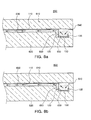
- FIG. 7a is a schematic sectional view of an antenna pattern frame according to a second exemplary embodiment of the present invention.
- FIG. 7b is a schematic sectional view showing the filling of a mold with a resin material for manufacturing an antenna pattern frame to manufacture the antenna pattern frame of FIG. 7a ;
- FIG. 8a is a schematic sectional view of an antenna pattern frame according to a third exemplary embodiment of the present invention.
- FIG. 8b is a schematic sectional view showing the filling of a mold with a resin material for manufacturing an antenna pattern frame to manufacture the antenna pattern frame of FIG. 8a ;
- FIG. 9 is a schematic view showing an electronic device case including an antenna pattern radiator embedded therein according to another exemplary embodiment of the present invention.
- FIG. 10 is a schematic sectional view showing the filling of a mold with a resin material for manufacturing an electronic device case to manufacture the electronic device case including the antenna pattern embedded therein according to another exemplary embodiment of the present invention
- FIGS. 11a to 11c are schematic sectional view showing an electronic device case including an antenna pattern radiator embedded therein according to another exemplary embodiment of the present invention.
- FIG. 12 is a schematic sectional view showing the providing of elasticity to a connection terminal part in manufacturing the electronic device case including the antenna pattern embedded therein according to another exemplary embodiment of the present invention.
- FIG. 13 is a schematic sectional view showing the inserting of an elastic member in manufacturing the electronic device case including the antenna pattern embedded therein according to another exemplary embodiment of the present invention.
- FIG. 1 is a schematic perspective view showing a case of a mobile communication terminal, an electronic device, with a cutaway portion according to an exemplary embodiment of the present invention
- FIG. 2 is an exploded schematic perspective view of the mobile communication terminal manufactured by using an antenna pattern frame according to an exemplary embodiment of the present invention.
- a radiator 100 including an antenna pattern part 110 may be embedded in a case 300 of a mobile communication device 400, an electronic device, according to an exemplary embodiment of the present invention.
- a radiator frame 210 having the antenna pattern formed thereon is required.
- the radiator 100 may include a connection terminal part 130 to be connected to a terminal 510 of a circuit board 500, and as the connection terminal part 130 is connected to the circuit board 500, the electronic device case 300 may implement an antenna performance in the mobile communication terminal 400.
- a fastening part 320 may be provided to at least one side of the electronic device case 300 in which the antenna pattern part 110 is embedded, so as to be fastened to a main case 520 forming an external appearance of the mobile communication terminal 400 as an electronic device.
- the fastening part 320 is protruded from one side of the electronic device case 300 in which the antenna pattern is embedded.
- the main case 520 includes a fastening line recess 525 corresponding to the fastening part 320, so that the fastening part 320 can be inserted into the fastening line recess 525 and slidably fastened thereto.
- the protruded fastening part 320 may be formed on the main case 520 and the fastening line recess 525 may be formed on the electronic device case 300 in which the antenna pattern is embedded, so as to be slidably fastened thereto.
- FIGS. 3a to 3c are schematic perspective views of a radiator provided to the antenna frame according to an exemplary embodiment of the present invention.
- An antenna pattern frame 200 is manufactured by injection-molding the radiator 100, and the radiator 100 provided to the antenna pattern frame 200 may include an antenna pattern part 110 for transmitting or receiving a signal and a connection terminal part 130 allowing the signal to be transmitted to or received from the circuit board 500.
- the radiator 100 provided to the antenna pattern frame 200 may include the antenna pattern part 100, the connection part 120, and the connection terminal part 130.
- the radiator 100 formed as a conductor made of aluminum or copper, receives an external signal and transfers the received signal to a signal processing unit of an electronic device such as the mobile communication terminal 400. Also, the radiator 100 may include the antenna pattern part 110 forming a meander line to receive external signals of various bands.
- the radiator 100 may include the antenna pattern part 110 for receiving an external signal and the connection terminal part 130 in contact with the circuit board 500 of the electronic device in order to transmit the external signal.
- the antenna pattern part 110 and the connection terminal part 130 of the radiator 100 may be bent to have a three-dimensional structure, and the antenna pattern part 110 and the antenna terminal part 130 may be connected by the connection part 120.
- connection part 120 allows the antenna pattern part 110 and the connection terminal part 130 to be formed on different planes, and allows the connection terminal part 130, which is not embedded in the electronic device case 300, to be exposed from the opposite side of one side on which the antenna pattern part 110 is formed.
- connection terminal part 130 allows a signal received from the antenna pattern part 110 to be transmitted to the circuit board 500 of the electronic device, and preferably, the connection terminal part 130 is in point-contact with the terminal 510 of the circuit board 500 in order to secure reliability in the signal transmission.
- connection terminal part 130 may include a contact projection 130a to be in point-contact with the circuit board 500 of the electronic device, and as the protruded contact projection 130a is in contact with the terminal 510 of the circuit board 500, the reliability of the signal transmission through the point contact can be obtained.
- connection terminal part 130 may have a bent portion 135 formed by bending the connection terminal part 130 in order to provide the contact projection 130a, and the contact projection 130a may be formed on the bent portion 135.
- a reinforcing portion 135b may be formed at the boundary between the connection part 120 and the connection terminal part 130.
- the reinforcing portion 130b may be configured to secure an elastic force of the connection terminal part 130. After the antenna pattern-embedded electronic device case 300 is injection-molded, the connection terminal part 130 is bent by applying an external force to provide elasticity to the connection terminal part 130, and in this case, the reinforcing portion 130b is formed at the boundary between the connection part 120 and the connection terminal part 130 to secure the elastic force of the connection terminal part 130.
- the presence of the reinforcing portion 130b strengthens the boundary between the connection part 120 and the connection terminal part 130, and prevents the connection terminal part 130 from being damaged by an external impact.
- the reinforcing portion 130b may be a reinforcing bead formed to be protruded from the boundary between the connection part 120 and the connection terminal part 130 or may be formed by rounding the boundary between the connection part 120 and the connection terminal part 130.
- the reinforcing part 130b may not be limited to the reinforcing bead 130b or the rounded configuration, and any means may be used so long as it can secure an elastic force of the connection terminal part 130 and prevent the connection terminal part 130 from being damaged by an external force.
- FIGS. 4 and 5a to 5c are schematic perspective views of the antenna pattern frame according to an exemplary embodiment of the present invention.
- FIGS. 6a , 7a , and 8a are schematic sectional views of the antenna pattern frame according to first to third exemplary embodiments of the present invention ( FIG. 6a is a sectional view taken along line A-A in FIG. 4 ), and
- FIGS.6b , 7b, and 8b are schematic sectional views showing the filling of a mold with a resin material for manufacturing an antenna pattern frame to manufacture the antenna pattern frames of FIG. 6a , 7a , and 8a .
- the antenna pattern frame 200 may include the radiator 100 and the radiator frame 210.
- the configuration of the radiator 210 has been described in detail, so a repeated description thereof will be omitted.
- the radiator frame 210 may be manufactured as the radiator 100 is injection-molded and separated from the connection terminal part 130 to allow the connection terminal part 130 to have elasticity, and may have a radiator support protruded from the opposite surface 210b of one surface 210a on which the antenna pattern part 110 is formed.
- the radiator frame 210 is an injection-molded structure, and the antenna pattern part 110 may be formed on one surface 210a of the radiator frame 210 and the connection terminal part 130 may be formed on the opposite surface 210b of the one surface 210a.
- the one surface 210a, with the antenna pattern part 110 formed thereon, of the radiator frame 210 may be attached at the inner side of the electronic device case 300 to embed the antenna pattern at the inner side of the electronic device case 300.
- the radiator support 220 integrally formed with the radiator frame 210, will be described later when a mold and method for manufacturing the antenna pattern frame 200 are explained.
- the radiator 100 is inserted into an internal space 630 of an antenna pattern frame manufacturing mold 600.
- the radiator 100 including the antenna pattern part 110 for transmitting or receiving a signal and a connection terminal part 130 for allowing the signal to be transmitted to or received from the circuit board 500 of the electronic device, which are formed on the mutually different planes of the radiator 100, is disposed in the internal space 630 of the antenna pattern frame manufacturing mold 600.
- the radiator 100 may include the contact projection 130a and the reinforcing portion130b as mentioned above.
- the antenna pattern frame manufacturing mold 600 may have the internal space 630 in which the radiator 100 is accommodated, and the internal space 630 may be generated as upper and lower molds 610 and 620 of the antenna pattern frame manufacturing mold 600 are combined.
- the internal space 630 is formed as the upper mold 610 and the lower mold 620 are combined, and a recess formed on the upper mold 610 or the lower mold 620 may constitute the internal space 630 when the upper mold 610 and the lower mold 620 are combined.
- a resin material injection portion 640 may be formed on the upper mold 610, the lower mold 620, or any one of the upper and lower molds 610 and 620 to allow a resin material to be introduced into the internal space 630 to form the radiator frame 210 allowing the antenna pattern part 110 to be embedded at the inner side of the electronic device 300 according to the internal space 630 of the upper and lower molds 610 and 620 when the upper and lower molds 610 and 620 are combined.
- the resin material is filled such that the radiator 100 has the same boundary surface with the radiator frame 210 in order to smooth a flow of the resin material when the radiator frame 210 is put in the mold and injection-molded to manufacture the electronic device case 300 in which the antenna pattern is embedded.
- the internal space 630 of the upper and lower molds 610 and 620 may have an accommodation recess 650 for accommodating the connection part 120 and the connection terminal part 130 of the radiator 100.
- the resin material may be introduced into the accommodation recess 650 to fixedly support the connection part 120 and the connection terminal part 130.
- connection part 120 is in contact with one side of the accommodation recess 650, the resin material can be filled on one side of the connection part 120 to form the radiator support 220.
- the radiator support 220 formed by the resin material introduced into the accommodation recess 650 may be protruded from the opposite side of one side on which the antenna pattern part 110 is formed.
- connection part 120 and the connection terminal part 130 may be accommodated in the accommodation recess 650 formed on the lower mold 620 of the antenna pattern frame manufacturing mold 600.
- connection part 120 and the connection terminal part 130 are inserted into the space without being in contact with the side of the accommodation recess 650 and the resin material can be in contact with the both sides of the connection part 120.
- the resin material is in contact with both sides of the connection part 120, the resin material becomes an injection reinforcing part 230 (to be described), and the resin material in contact with the other side becomes the radiator support 220.
- connection terminal part 130 is bent by applying an external force in order to provide elasticity to the connection terminal part 130 in forming the electronic device case 300 having an antenna pattern embedded therein, and at this time, the injection reinforcing portion 230 serves to prevent the connection part 120 from being released from the radiator support 220.
- the depth of the accommodation recess 650 formed on the lower mold 620 of the antenna pattern frame manufacturing mold 600 may be different.
- the injection reinforcing portion 230 supporting one side of the connection part 120 may serve to prevent the connection part 120 from being released from the radiator support 220, and because no resin material is filled in the boundary between the connection part 120 and the connection terminal part 130, the connection terminal part 130 can be effectively bent in providing elasticity to the connection terminal part 130.
- FIG. 9 is a schematic view showing an electronic device case including an antenna pattern radiator embedded therein according to another exemplary embodiment of the present invention.
- FIG. 10 is a schematic sectional view showing the filling of a mold with a resin material for manufacturing an electronic device case to manufacture the electronic device case including the antenna pattern embedded therein according to another exemplary embodiment of the present invention.
- FIGS. 11a to 11c are schematic sectional views showing an electronic device case including an antenna pattern radiator embedded therein according to another exemplary embodiment of the present invention.
- the electronic device case 300 having an antenna pattern embedded therein may include an antenna pattern frame 200 and a case frame 310.
- the case frame 310 may be a separate injection-molded product having a radiator accommodation recess 310a having a shape corresponding to the radiator frame 210, and the electronic device case 300 including the antenna pattern radiator embedded therein can be manufactured by attaching the radiator frame 210 to the radiator accommodation recess 310a.
- the antenna pattern frame 200 formed by integrating the radiator 100 and the radiator frame 210 is disposed in an electronic device case manufacturing mold 700 including an internal space 730, and a resin material is introduced thereinto to integrate the radiator frame 210 to the electronic device case 300.
- the radiator frame 210 and the case frame 310 may be formed without a boundary discriminated therebetween.
- a resin material injection portion 740 may be formed on the upper mold, the lower mold, or on both the upper and lower molds 710 and 720 of the electronic device case manufacturing mold in which the antenna pattern frame 200 having the radiator 100 is accommodated.
- the resin material injection portion 740 allows a resin material to be introduced into the internal space 730 to form the electronic device case 300 according to the internal space 730 formed within the mold 700.
- the antenna pattern frame 200 and the case frame 310 may be integrated to form the electronic device case 300 having the antenna pattern embedded therein.
- connection terminal part 130 the method for providing elasticity to the connection terminal part 130 will now be described.
- a process is performed to provide elasticity to the connection terminal part 130 of the electronic device case 300 having the antenna pattern embedded therein completely formed by introducing the resin material into the electronic device case manufacturing mold 700.
- connection terminal part 130 can be provided with elasticity through a process of separating the connection terminal part 130 in contact with the radiator support 220 by using an external force.
- connection part 120 can be prevented from being released from the radiator support 220 by means of the foregoing injection reinforcing portion 230, and the reinforcing portion 130b may be provided to the boundary between the connection part 120 and the connection terminal part 130.
- the presence of the reinforcing portion 130b can further strengthen the boundary between the connection part 120 and the connection terminal part 130, and prevent the connection terminal part 130 from being damaged by an external impact.
- FIG. 12 is a schematic sectional view showing providing of elasticity to a connection terminal part in manufacturing the electronic device case including the antenna pattern embedded therein according to another exemplary embodiment of the present invention
- FIG. 13 is a schematic sectional view showing the inserting of an elastic member in manufacturing the electronic device case including the antenna pattern embedded therein according to another exemplary embodiment of the present invention.
- connection terminal part 130 of the electronic device case 300 having the antenna pattern embedded therein completely formed by introducing the resin material into the electronic device case manufacturing mold 700 to release the connection terminal part 130 from the radiator support 220.
- connection terminal part 130 released from the radiator support 220 is provided with elasticity by a space 225 between the radiator support part 220 and the connection terminal part 130, or an elastic member 240 may be inserted into the space 225.
- the elastic member 240 may be made of at least one of silicon or rubber, an insulating material, as a member for increasing elasticity of the connection terminal part 130.
- connection terminal part 130 comes into contact with the terminal 510 of the circuit board 500, it can be effectively make an electrical connection by virtue of the elastic member 240, and a stable structure can be secured for a signal transmission.
- the elastic member 240 is not an essential component of the electronic device case 300 having the antenna pattern embedded therein, and the purpose of the present invention can be achieved only with the connection terminal part 130 formed to be separated from the radiator support 220.
- connection terminal part 130 of the electronic device case 300 having the antenna pattern embedded therein has elasticity, it can be electrically connected to the circuit board without using any additional element, and can be prevented from being short-circuited by an external impact by securing a stable structure for a signal transmission.
- the electronic device including the electronic device case 300 having the antenna pattern embedded therein can be reduced in size.
- connection terminal part of the radiator has elasticity, it can be electrically connected to the main circuit board without using any additional element.
Abstract
Description
- This application claims the priority of Korean Patent Application No.
10-2010-0063078 filed on June 30, 2010 - The present invention relates to an electronic device case having an antenna pattern embedded therein, a method for manufacturing the same, a mold for manufacturing an antenna pattern frame, and an electronic device, and more particularly, to an electronic device case including an antenna radiator having an altered connection terminal part structure, a method for manufacturing the same, a mold for manufacturing an antenna pattern frame, and an electronic device.
- Mobile communication terminals such as a mobile phone, a personal digital assistant (PDA), a navigation device, a notebook computer, and the like, supporting radio communications are requisite devices in modern society. Mobile communication terminals are evolving to have additional functions such as CDMA, wireless LAN, GSM, DMB, and the like, and one of the most important components enabling these functions is an antenna.
- Antennas employed for mobile communication terminals have evolved from an external type antenna such as a rod antenna or a helical antenna to an internal type antenna disposed within a terminal.
- The external type antenna is vulnerable to an external impact, and the internal type antenna leads to an increase in the volume of a terminal.
- Thus, in order to solve the problem, research into the integration of an antenna into a mobile communication terminal is actively ongoing.
- In the related art, a radiator is injection-molded to form an antenna pattern frame, and the antenna pattern frame is injection-molded again so as to allow the radiator be embedded in an electronic device case.
- A connection terminal part of the embedded radiator needs to be in contact with a main circuit board for an electrical connection therebetween in the terminal. As the connection terminal part of the related art does not have elasticity and has a planar surface or a curved surface, the connection terminal is in use without any movement.
- Thus, in order to connect the connection terminal part to the main circuit board, an additional element having elasticity is added to the main circuit board to allow the connection terminal part to be brought into contact with the main circuit board thereby, causing a problem in that a unit cost increases as a result of the addition of the element.
- In addition, the additionally performed process of adding the additional element lengthens the manufacturing time and the additional element is deformed or released from its original position due to an external impact applied thereto, causing a problem of a short circuit to result in the degradation of the ability of a product to compete in the marketplace.
- An aspect of the present invention provides an electronic device case having an antenna pattern embedded therein, a manufacturing method thereof, and an electronic device.
- Another aspect of the present invention provides a manufacturing mold for manufacturing an antenna pattern frame provided to an electronic device case.
- Another aspect of the present invention provides an electronic device case having an antenna pattern embedded therein, capable of securing a stable structure in transferring an antenna signal, thus preventing the occurrence of a short circuit due to an external impact.
- According to an aspect of the present invention, there is provided an electronic device case including: a radiator including an antenna pattern part transmitting or receiving a signal and a connection terminal part allowing the signal to be transmitted to or received from a circuit board of an electronic device; a radiator frame including the radiator injection-molded thereon, separated from the connection terminal part so that the connection part can have elasticity, and having a radiator support protruded from the opposite surface of one surface on which the antenna pattern part is formed; and a case frame covering one surface of the radiator frame to allow the antenna pattern part to be embedded between the case frame and the radiator frame.
- The connection terminal part may include a contact projection formed to be in point-contact with the circuit board.
- The connection terminal part may include a bent portion formed by bending one end of the connection terminal part, and the contact projection may be formed on the bent portion.
- The electronic device case may further include: an elastic member provided between the connection terminal part and the radiator support to increase the elasticity of the connection terminal part.
- The elastic member may be made of at least one of silicon or rubber as an insulating material.
- The radiator may include a connection part, as part of the radiator, connecting the antenna pattern part and the connection terminal part, and the connection part may connect the antenna pattern part and the connection terminal part such that the antenna pattern part is formed on one surface of the radiator frame and the connection terminal part is formed on the opposite surface of the one surface.
- The connection part may be supported such that one surface of the connection part is in contact with the radiator support.
- The electronic device case may further include: at least one reinforcing portion formed at the boundary between the connection part and the connection terminal part to secure an elastic force of the connection terminal part.
- The reinforcing portion may be a reinforcing bead formed to be protruded at the boundary between the connection part and the connection terminal part.
- The reinforcing portion may be formed make the boundary between the connection part and the connection terminal part rounded.
- The electronic device case may further include: an injection reinforcing portion formed to be in contact with one side of the connection part to prevent the connection part from being released from the radiator support.
- The injection reinforcing portion may be integrally formed with the radiator frame.
- According to another aspect of the present invention, there is provided an electronic device including: an electronic device case including an antenna pattern embedded therein; and a circuit board connected to a connection terminal part to transmit and receive a signal of a radiator.
- The electronic device case may include a fastening part formed on at least one side of the electronic device case and coupled with a main case forming an external appearance of the electronic device.
- The fastening part may be protruded from one side of the electronic device case having the antenna pattern embedded therein, and the main case includes a fastening line recess corresponding to the fastening part to allow the fastening part to be inserted into the fastening line recess and slidably coupled therein.
- According to another aspect of the present invention, there is provided a mold for manufacturing an antenna pattern frame, including: upper and lower molds in which a radiator, including an antenna pattern part for transmitting and receiving a signal, a connection terminal part connected to a circuit board of an electronic device, and a connection part connecting the antenna pattern part and the connection terminal part, is accommodated; and a resin material injection part formed on the upper mold, the lower mold or on at least one of the upper and lower molds to allow a resin material to be introduced into an internal space between the upper and lower molds so as to form a radiator frame allowing the antenna pattern to be embedded in the interior of the electronic device by the internal space between the upper and lower molds when the upper and lower molds are combined, wherein the lower mold includes an accommodation recess for accommodating the connection part and the connection terminal part, the resin material is introduced into the accommodation recess to support both sides of the connection part, and the radiator becomes the radiator frame by the internal space.
- The accommodation recess may have different depths based on the connection part as a boundary so that portions supporting the side of the connection part can be different.
- According to another aspect of the present invention, there is provided a method for manufacturing an electronic device case having an antenna pattern embedded therein, including: injection-molding a radiator frame having a radiator such that an antenna pattern part for transmitting and receiving a signal and a connection terminal part allowing the signal to be transmitted to or received from a circuit board of an electronic device are disposed on different planes of the radiator; injection-molding a case frame covering one surface of the radiator frame to make the antenna pattern part embedded between the case frame and the radiator frame; and separating the connection terminal part from the case frame and providing elasticity to the connection terminal part.
- The radiator frame may include a radiator support protruded from the opposite surface of one surface on which the antenna pattern part is formed in order to allow the connection terminal part to have elasticity.
- The method may further include: inserting an elastic member between the connection terminal part and the case frame in order to increase the elasticity of the connection terminal part, after elasticity is provided to the connection terminal part.
- The elastic member may be made of at least one of silicon or rubber as an insulating material.
- The radiator may include a connection part, as part of the radiator, connecting the antenna pattern part and the connection terminal part such that the antenna pattern part and the connection terminal part are positioned on different planes, and may include at least one reinforcing portion formed at a boundary between the connection part and the connection terminal part to secure an elastic force of the connection terminal part.
- The radiator frame may include a radiator support protruded from the opposite surface of one surface on which the antenna pattern part is formed to allow the connection terminal part to have elasticity, and the connection part may be supported such that one side of the connection part is in contact with the radiator support.
- The above and other aspects, features and other advantages of the present invention will be more clearly understood from the following detailed description taken in conjunction with the accompanying drawings, in which:
-
FIG. 1 is a schematic perspective view showing a case of a mobile communication terminal, an electronic device, with a cutaway portion according to an exemplary embodiment of the present invention; -
FIG. 2 is an exploded schematic perspective view of the mobile communication terminal manufactured by using an antenna pattern frame according to an exemplary embodiment of the present invention; -
FIGS. 3a to 3c are schematic perspective views of a radiator provided to the antenna frame according to an exemplary embodiment of the present invention; -
FIGS. 4 and5a to 5c are schematic perspective views of the antenna pattern frame according to an exemplary embodiment of the present invention; -
FIG. 6a is a schematic sectional view of an antenna pattern frame taken along line A-A ofFIG. 4a according to a first exemplary embodiment of the present invention; -
FIG. 6b is a schematic sectional view showing the filling of a mold with a resin material for manufacturing an antenna pattern frame to manufacture the antenna pattern frame ofFIG. 6a ; -
FIG. 7a is a schematic sectional view of an antenna pattern frame according to a second exemplary embodiment of the present invention; -
FIG. 7b is a schematic sectional view showing the filling of a mold with a resin material for manufacturing an antenna pattern frame to manufacture the antenna pattern frame ofFIG. 7a ; -
FIG. 8a is a schematic sectional view of an antenna pattern frame according to a third exemplary embodiment of the present invention; -
FIG. 8b is a schematic sectional view showing the filling of a mold with a resin material for manufacturing an antenna pattern frame to manufacture the antenna pattern frame ofFIG. 8a ; -
FIG. 9 is a schematic view showing an electronic device case including an antenna pattern radiator embedded therein according to another exemplary embodiment of the present invention; -
FIG. 10 is a schematic sectional view showing the filling of a mold with a resin material for manufacturing an electronic device case to manufacture the electronic device case including the antenna pattern embedded therein according to another exemplary embodiment of the present invention; -
FIGS. 11a to 11c are schematic sectional view showing an electronic device case including an antenna pattern radiator embedded therein according to another exemplary embodiment of the present invention; -
FIG. 12 is a schematic sectional view showing the providing of elasticity to a connection terminal part in manufacturing the electronic device case including the antenna pattern embedded therein according to another exemplary embodiment of the present invention; and -
FIG. 13 is a schematic sectional view showing the inserting of an elastic member in manufacturing the electronic device case including the antenna pattern embedded therein according to another exemplary embodiment of the present invention. - Exemplary embodiments of the present invention will now be described in detail with reference to the accompanying drawings. The invention may, however, be embodied in many different forms and should not be construed as being limited to the embodiments set forth herein. Rather, these embodiments are provided so that this disclosure will be thorough and complete, and will fully convey the scope of the invention to those skilled in the art.
- In the drawings, the shapes and dimensions may be exaggerated for clarity, and the same reference numerals will be used throughout to designate the same or like components.
-
FIG. 1 is a schematic perspective view showing a case of a mobile communication terminal, an electronic device, with a cutaway portion according to an exemplary embodiment of the present invention, andFIG. 2 is an exploded schematic perspective view of the mobile communication terminal manufactured by using an antenna pattern frame according to an exemplary embodiment of the present invention. - With reference to
FIGS. 1 and2 , aradiator 100 including anantenna pattern part 110 may be embedded in acase 300 of amobile communication device 400, an electronic device, according to an exemplary embodiment of the present invention. - In order to embed the
antenna pattern part 110 within theelectronic device case 300, aradiator frame 210 having the antenna pattern formed thereon is required. - Here, the
radiator 100 may include aconnection terminal part 130 to be connected to aterminal 510 of acircuit board 500, and as theconnection terminal part 130 is connected to thecircuit board 500, theelectronic device case 300 may implement an antenna performance in themobile communication terminal 400. - A
fastening part 320 may be provided to at least one side of theelectronic device case 300 in which theantenna pattern part 110 is embedded, so as to be fastened to amain case 520 forming an external appearance of themobile communication terminal 400 as an electronic device. - The
fastening part 320 is protruded from one side of theelectronic device case 300 in which the antenna pattern is embedded. Themain case 520 includes afastening line recess 525 corresponding to thefastening part 320, so that thefastening part 320 can be inserted into thefastening line recess 525 and slidably fastened thereto. - Alternatively, the protruded
fastening part 320 may be formed on themain case 520 and thefastening line recess 525 may be formed on theelectronic device case 300 in which the antenna pattern is embedded, so as to be slidably fastened thereto. - Antenna pattern frame, and mold and method for manufacturing the antenna pattern frame
-
FIGS. 3a to 3c are schematic perspective views of a radiator provided to the antenna frame according to an exemplary embodiment of the present invention. - An
antenna pattern frame 200 is manufactured by injection-molding theradiator 100, and theradiator 100 provided to theantenna pattern frame 200 may include anantenna pattern part 110 for transmitting or receiving a signal and aconnection terminal part 130 allowing the signal to be transmitted to or received from thecircuit board 500. - With reference to
FIGS. 3a to 3c , theradiator 100 provided to theantenna pattern frame 200 according to an exemplary embodiment of the present invention may include theantenna pattern part 100, theconnection part 120, and theconnection terminal part 130. - The
radiator 100, formed as a conductor made of aluminum or copper, receives an external signal and transfers the received signal to a signal processing unit of an electronic device such as themobile communication terminal 400. Also, theradiator 100 may include theantenna pattern part 110 forming a meander line to receive external signals of various bands. - The
radiator 100 may include theantenna pattern part 110 for receiving an external signal and theconnection terminal part 130 in contact with thecircuit board 500 of the electronic device in order to transmit the external signal. - Also, the
antenna pattern part 110 and theconnection terminal part 130 of theradiator 100 may be bent to have a three-dimensional structure, and theantenna pattern part 110 and theantenna terminal part 130 may be connected by theconnection part 120. - The
connection part 120 allows theantenna pattern part 110 and theconnection terminal part 130 to be formed on different planes, and allows theconnection terminal part 130, which is not embedded in theelectronic device case 300, to be exposed from the opposite side of one side on which theantenna pattern part 110 is formed. - Here, the
connection terminal part 130 allows a signal received from theantenna pattern part 110 to be transmitted to thecircuit board 500 of the electronic device, and preferably, theconnection terminal part 130 is in point-contact with theterminal 510 of thecircuit board 500 in order to secure reliability in the signal transmission. - Thus, the
connection terminal part 130 may include acontact projection 130a to be in point-contact with thecircuit board 500 of the electronic device, and as theprotruded contact projection 130a is in contact with theterminal 510 of thecircuit board 500, the reliability of the signal transmission through the point contact can be obtained. - Here, the
connection terminal part 130 may have abent portion 135 formed by bending theconnection terminal part 130 in order to provide thecontact projection 130a, and thecontact projection 130a may be formed on thebent portion 135. - A reinforcing portion 135b may be formed at the boundary between the
connection part 120 and theconnection terminal part 130. - The reinforcing
portion 130b may be configured to secure an elastic force of theconnection terminal part 130. After the antenna pattern-embeddedelectronic device case 300 is injection-molded, theconnection terminal part 130 is bent by applying an external force to provide elasticity to theconnection terminal part 130, and in this case, the reinforcingportion 130b is formed at the boundary between theconnection part 120 and theconnection terminal part 130 to secure the elastic force of theconnection terminal part 130. - The presence of the reinforcing
portion 130b strengthens the boundary between theconnection part 120 and theconnection terminal part 130, and prevents theconnection terminal part 130 from being damaged by an external impact. - Here, the reinforcing
portion 130b may be a reinforcing bead formed to be protruded from the boundary between theconnection part 120 and theconnection terminal part 130 or may be formed by rounding the boundary between theconnection part 120 and theconnection terminal part 130. - However, the reinforcing
part 130b may not be limited to the reinforcingbead 130b or the rounded configuration, and any means may be used so long as it can secure an elastic force of theconnection terminal part 130 and prevent theconnection terminal part 130 from being damaged by an external force. -
FIGS. 4 and5a to 5c are schematic perspective views of the antenna pattern frame according to an exemplary embodiment of the present invention.FIGS. 6a ,7a , and8a are schematic sectional views of the antenna pattern frame according to first to third exemplary embodiments of the present invention (FIG. 6a is a sectional view taken along line A-A inFIG. 4 ), andFIGS.6b ,7b, and 8b are schematic sectional views showing the filling of a mold with a resin material for manufacturing an antenna pattern frame to manufacture the antenna pattern frames ofFIG. 6a ,7a , and8a . - With reference to
FIGS. 4 ,5a , and5c , theantenna pattern frame 200 may include theradiator 100 and theradiator frame 210. - Here, the configuration of the
radiator 210 has been described in detail, so a repeated description thereof will be omitted. - The
radiator frame 210 may be manufactured as theradiator 100 is injection-molded and separated from theconnection terminal part 130 to allow theconnection terminal part 130 to have elasticity, and may have a radiator support protruded from theopposite surface 210b of onesurface 210a on which theantenna pattern part 110 is formed. - Namely, the
radiator frame 210 is an injection-molded structure, and theantenna pattern part 110 may be formed on onesurface 210a of theradiator frame 210 and theconnection terminal part 130 may be formed on theopposite surface 210b of the onesurface 210a. - The one
surface 210a, with theantenna pattern part 110 formed thereon, of theradiator frame 210 may be attached at the inner side of theelectronic device case 300 to embed the antenna pattern at the inner side of theelectronic device case 300. - The
radiator support 220, integrally formed with theradiator frame 210, will be described later when a mold and method for manufacturing theantenna pattern frame 200 are explained. - With reference to
FIGS. 6a and 6b , in manufacturing theantenna pattern frame 200 according to a first exemplary embodiment of the present invention, theradiator 100 is inserted into aninternal space 630 of an antenna patternframe manufacturing mold 600. - Namely, the
radiator 100, including theantenna pattern part 110 for transmitting or receiving a signal and aconnection terminal part 130 for allowing the signal to be transmitted to or received from thecircuit board 500 of the electronic device, which are formed on the mutually different planes of theradiator 100, is disposed in theinternal space 630 of the antenna patternframe manufacturing mold 600. - Here, the
radiator 100 may include thecontact projection 130a and the reinforcing portion130b as mentioned above. - The antenna pattern
frame manufacturing mold 600 may have theinternal space 630 in which theradiator 100 is accommodated, and theinternal space 630 may be generated as upper andlower molds frame manufacturing mold 600 are combined. - Namely, the
internal space 630 is formed as theupper mold 610 and thelower mold 620 are combined, and a recess formed on theupper mold 610 or thelower mold 620 may constitute theinternal space 630 when theupper mold 610 and thelower mold 620 are combined. - A resin
material injection portion 640 may be formed on theupper mold 610, thelower mold 620, or any one of the upper andlower molds internal space 630 to form theradiator frame 210 allowing theantenna pattern part 110 to be embedded at the inner side of theelectronic device 300 according to theinternal space 630 of the upper andlower molds lower molds - The resin material is filled such that the
radiator 100 has the same boundary surface with theradiator frame 210 in order to smooth a flow of the resin material when theradiator frame 210 is put in the mold and injection-molded to manufacture theelectronic device case 300 in which the antenna pattern is embedded. - Also, the
internal space 630 of the upper andlower molds accommodation recess 650 for accommodating theconnection part 120 and theconnection terminal part 130 of theradiator 100. The resin material may be introduced into theaccommodation recess 650 to fixedly support theconnection part 120 and theconnection terminal part 130. - Namely, because one side of the
connection part 120 is in contact with one side of theaccommodation recess 650, the resin material can be filled on one side of theconnection part 120 to form theradiator support 220. - Here, the
radiator support 220 formed by the resin material introduced into theaccommodation recess 650 may be protruded from the opposite side of one side on which theantenna pattern part 110 is formed. - With reference to
FIGS. 7a and 7b , theconnection part 120 and theconnection terminal part 130 may be accommodated in theaccommodation recess 650 formed on thelower mold 620 of the antenna patternframe manufacturing mold 600. - In this case, the
connection part 120 and theconnection terminal part 130 are inserted into the space without being in contact with the side of theaccommodation recess 650 and the resin material can be in contact with the both sides of theconnection part 120. - Namely, because the resin material is in contact with both sides of the
connection part 120, the resin material becomes an injection reinforcing part 230 (to be described), and the resin material in contact with the other side becomes theradiator support 220. - Here, the
connection terminal part 130 is bent by applying an external force in order to provide elasticity to theconnection terminal part 130 in forming theelectronic device case 300 having an antenna pattern embedded therein, and at this time, theinjection reinforcing portion 230 serves to prevent theconnection part 120 from being released from theradiator support 220. - With reference to
FIGS. 8a and 8b , the depth of theaccommodation recess 650 formed on thelower mold 620 of the antenna patternframe manufacturing mold 600 may be different. - This is to make the portion supporting the side of the
connection part 120 after the resin material is introduced into theaccommodation recess 650 different. - As mentioned above, the
injection reinforcing portion 230 supporting one side of theconnection part 120 may serve to prevent theconnection part 120 from being released from theradiator support 220, and because no resin material is filled in the boundary between theconnection part 120 and theconnection terminal part 130, theconnection terminal part 130 can be effectively bent in providing elasticity to theconnection terminal part 130. - Electronic device case having antenna pattern embedded therein, and a mold and method for manufacturing the same
-
FIG. 9 is a schematic view showing an electronic device case including an antenna pattern radiator embedded therein according to another exemplary embodiment of the present invention.FIG. 10 is a schematic sectional view showing the filling of a mold with a resin material for manufacturing an electronic device case to manufacture the electronic device case including the antenna pattern embedded therein according to another exemplary embodiment of the present invention.FIGS. 11a to 11c are schematic sectional views showing an electronic device case including an antenna pattern radiator embedded therein according to another exemplary embodiment of the present invention. - With reference to
FIGS. 9 and 10 , theelectronic device case 300 having an antenna pattern embedded therein may include anantenna pattern frame 200 and acase frame 310. - The
case frame 310 may be a separate injection-molded product having aradiator accommodation recess 310a having a shape corresponding to theradiator frame 210, and theelectronic device case 300 including the antenna pattern radiator embedded therein can be manufactured by attaching theradiator frame 210 to theradiator accommodation recess 310a. - In manufacturing the
electronic device case 300 including the antenna pattern radiator, theantenna pattern frame 200 formed by integrating theradiator 100 and theradiator frame 210 is disposed in an electronic devicecase manufacturing mold 700 including aninternal space 730, and a resin material is introduced thereinto to integrate theradiator frame 210 to theelectronic device case 300. - The
radiator frame 210 and thecase frame 310 may be formed without a boundary discriminated therebetween. - Here, a resin
material injection portion 740 may be formed on the upper mold, the lower mold, or on both the upper andlower molds antenna pattern frame 200 having theradiator 100 is accommodated. Thus, when the upper andlower molds material injection portion 740 allows a resin material to be introduced into theinternal space 730 to form theelectronic device case 300 according to theinternal space 730 formed within themold 700. - Through the foregoing process, the
antenna pattern frame 200 and thecase frame 310 may be integrated to form theelectronic device case 300 having the antenna pattern embedded therein. - Here, the method for providing elasticity to the
connection terminal part 130 will now be described. - With reference to
FIGS. 11a to 11c , a process is performed to provide elasticity to theconnection terminal part 130 of theelectronic device case 300 having the antenna pattern embedded therein completely formed by introducing the resin material into the electronic devicecase manufacturing mold 700. - Namely, the
connection terminal part 130 can be provided with elasticity through a process of separating theconnection terminal part 130 in contact with theradiator support 220 by using an external force. - In this case, the
connection part 120 can be prevented from being released from theradiator support 220 by means of the foregoinginjection reinforcing portion 230, and the reinforcingportion 130b may be provided to the boundary between theconnection part 120 and theconnection terminal part 130. - The presence of the reinforcing
portion 130b can further strengthen the boundary between theconnection part 120 and theconnection terminal part 130, and prevent theconnection terminal part 130 from being damaged by an external impact. -
FIG. 12 is a schematic sectional view showing providing of elasticity to a connection terminal part in manufacturing the electronic device case including the antenna pattern embedded therein according to another exemplary embodiment of the present invention, andFIG. 13 is a schematic sectional view showing the inserting of an elastic member in manufacturing the electronic device case including the antenna pattern embedded therein according to another exemplary embodiment of the present invention. - With reference to
FIGS. 12 and 13 , an external force is applied to theconnection terminal part 130 of theelectronic device case 300 having the antenna pattern embedded therein completely formed by introducing the resin material into the electronic devicecase manufacturing mold 700 to release theconnection terminal part 130 from theradiator support 220. - The
connection terminal part 130 released from theradiator support 220 is provided with elasticity by aspace 225 between theradiator support part 220 and theconnection terminal part 130, or anelastic member 240 may be inserted into thespace 225. - The
elastic member 240 may be made of at least one of silicon or rubber, an insulating material, as a member for increasing elasticity of theconnection terminal part 130. - Thus, when the
connection terminal part 130 comes into contact with theterminal 510 of thecircuit board 500, it can be effectively make an electrical connection by virtue of theelastic member 240, and a stable structure can be secured for a signal transmission. - The
elastic member 240 is not an essential component of theelectronic device case 300 having the antenna pattern embedded therein, and the purpose of the present invention can be achieved only with theconnection terminal part 130 formed to be separated from theradiator support 220. - Through the exemplary embodiments as described above, because the
connection terminal part 130 of theelectronic device case 300 having the antenna pattern embedded therein has elasticity, it can be electrically connected to the circuit board without using any additional element, and can be prevented from being short-circuited by an external impact by securing a stable structure for a signal transmission. - In addition, because an additional element for an electrical connection to the circuit board is not required, a space by more than a certain size for mounting the additional element on the circuit board can be reduced.
- Thus, the electronic device including the
electronic device case 300 having the antenna pattern embedded therein can be reduced in size. - As set forth above, in an electronic device case having an antenna pattern embedded therein, a method for manufacturing the same, a mold for manufacturing an antenna pattern frame, and an electronic device according to exemplary embodiments of the invention, because the connection terminal part of the radiator has elasticity, it can be electrically connected to the main circuit board without using any additional element.
- Also, because a stable structure is secured in transmitting a signal, a short-circuit cannot occur due to an external impact.
- In addition, because an additional element is not required for an electrical connection to the main circuit board, a space by more than a certain size otherwise due to the additional element can be reduced to achieve compactness.
- While the present invention has been shown and described in connection with the exemplary embodiments, it will be apparent to those skilled in the art that modifications and variations can be made without departing from the spirit and scope of the invention as defined by the appended claims.
Claims (23)
- An electronic device case having antenna pattern embedded therein, the electronic device case comprising:a radiator including an antenna pattern part transmitting or receiving a signal and a connection terminal part allowing the signal to be transmitted to or received from a circuit board of an electronic device;a radiator frame including the radiator injection-molded thereon, separated from the connection terminal part so that the connection part can have elasticity, and having a radiator support protruded from the opposite surface of one surface on which the antenna pattern part is formed; anda case frame covering one surface of the radiator frame to allow the antenna pattern part to be embedded between the case frame and the radiator frame.
- The electronic device case of claim 1, wherein the connection terminal part comprises a contact projection formed to be in point-contact with the circuit board.
- The electronic device case of claim 2, wherein the connection terminal part comprises a bent portion formed by bending one end of the connection terminal part, and the contact projection is formed on the bent portion.
- The electronic device case of claim 1, further comprising: an elastic member provided between the connection terminal part and the radiator support to increase the elasticity of the connection terminal part.
- The electronic device case of claim 4, wherein the elastic member is made of at least one of silicon or rubber as an insulating material.
- The electronic device case of claim 1, wherein the radiator comprises a connection part, as part of the radiator, connecting the antenna pattern part and the connection terminal part, and the connection part connects the antenna pattern part and the connection terminal part such that the antenna pattern part is formed on one surface of the radiator frame and the connection terminal part is formed on the opposite surface of the one surface.
- The electronic device case of claim 6, wherein the connection part is supported such that one surface of the connection part is in contact with the radiator support.
- The electronic device case of claim 6, further comprising: at least one reinforcing portion formed at the boundary between the connection part and the connection terminal part to secure an elastic force of the connection terminal part.
- The electronic device case of claim 8, wherein the reinforcing portion is a reinforcing bead formed to be protruded at the boundary between the connection part and the connection terminal part.
- The electronic device case of claim 8, wherein the reinforcing portion is formed make the boundary between the connection part and the connection terminal part rounded.
- The electronic device case of claim 6, further comprising: an injection reinforcing portion formed to be in contact with one side of the connection part to prevent the connection part from being released from the radiator support.
- The electronic device case of claim 11, wherein the injection reinforcing portion is integrally formed with the radiator frame.
- An electronic device comprising:an electronic device case having an antenna pattern embedded therein according to any one of claim 1 to claim 12; anda circuit board connected to a connection terminal part to transmit and receive a signal of a radiator.
- The electronic device of claim 13, wherein the electronic device case having antenna pattern embedded therein comprises a fastening part formed on at least one side of the electronic device case and coupled with a main case forming an external appearance of the electronic device.
- The electronic device of claim 14, wherein the fastening part is protruded from one side of the electronic device case having the antenna pattern embedded therein, and the main case includes a fastening line recess corresponding to the fastening part to allow the fastening part to be inserted into the fastening line recess and slidably coupled therein.
- A mold for manufacturing an antenna pattern frame, the mold comprising:upper and lower molds in which a radiator, including an antenna pattern part for transmitting and receiving a signal, a connection terminal part connected to a circuit board of an electronic device, and a connection part connecting the antenna pattern part and the connection terminal part, is accommodated; anda resin material injection part formed on the upper mold, the lower mold or on at least one of the upper and lower molds to allow a resin material to be introduced into an internal space between the upper and lower molds so as to form a radiator frame allowing the antenna pattern to be embedded in the interior of the electronic device by the internal space between the upper and lower molds when the upper and lower molds are combined,wherein the lower mold includes an accommodation recess for accommodating the connection part and the connection terminal part, the resin material is introduced into the accommodation recess to support both sides of the connection part, and the radiator becomes the radiator frame by the internal space.
- The mold of claim 16, wherein the accommodation recess has different depths based on the connection part as a boundary so that portions supporting the side of the connection part can be different.
- A method for manufacturing an electronic device case having an antenna pattern embedded therein, the method comprising:injection-molding a radiator frame having a radiator such that an antenna pattern part for transmitting and receiving a signal and a connection terminal part allowing the signal to be transmitted to or received from a circuit board of an electronic device are disposed on different planes of the radiator;injection-molding a case frame covering one surface of the radiator frame to make the antenna pattern part embedded between the case frame and the radiator frame; andseparating the connection terminal part from the case frame and providing elasticity to the connection terminal part.
- The method of claim 18, wherein the radiator frame comprises a radiator support protruded from the opposite surface of one surface on which the antenna pattern part is formed in order to allow the connection terminal part to have elasticity.
- The method of claim 18, further comprising:inserting an elastic member between the connection terminal part and the case frame in order to increase the elasticity of the connection terminal part, after elasticity is provided to the connection terminal part.
- The method of claim 20, wherein the elastic member is made of at least one of silicon or rubber as an insulating material.
- The method of claim 18, wherein the radiator comprises a connection part, as part of the radiator, connecting the antenna pattern part and the connection terminal part such that the antenna pattern part and the connection terminal part are positioned on different planes, and also comprises at least one reinforcing portion formed at a boundary between the connection part and the connection terminal part to secure an elastic force of the connection terminal part.
- The method of claim 22, wherein the radiator frame comprises a radiator support protruded from the opposite surface of one surface on which the antenna pattern part is formed to allow the connection terminal part to have elasticity, and the connection part is supported such that one side of the connection part is in contact with the radiator support.
Applications Claiming Priority (1)
| Application Number | Priority Date | Filing Date | Title |
|---|---|---|---|
| KR1020100063078A KR101153666B1 (en) | 2010-06-30 | 2010-06-30 | Case of electronic device having antenna pattern embeded therein, method for manufacturing the same, mould for manufacturing antenna pattern frame and electronic device |
Publications (2)
| Publication Number | Publication Date |
|---|---|
| EP2403065A2 true EP2403065A2 (en) | 2012-01-04 |
| EP2403065A3 EP2403065A3 (en) | 2013-01-02 |
Family
ID=44675509
Family Applications (1)
| Application Number | Title | Priority Date | Filing Date |
|---|---|---|---|
| EP11250424A Withdrawn EP2403065A3 (en) | 2010-06-30 | 2011-04-04 | Electronic device case having antenna pattern embedded therein, method for manufacturing the same, mold for manufacturing antenna pattern frame, and electronic device |
Country Status (5)
| Country | Link |
|---|---|
| US (1) | US20120001807A1 (en) |
| EP (1) | EP2403065A3 (en) |
| JP (1) | JP2012015991A (en) |
| KR (1) | KR101153666B1 (en) |
| CN (1) | CN102316688A (en) |
Cited By (1)
| Publication number | Priority date | Publication date | Assignee | Title |
|---|---|---|---|---|
| CN110299479A (en) * | 2019-06-26 | 2019-10-01 | Oppo广东移动通信有限公司 | Electronic equipment |
Families Citing this family (23)
| Publication number | Priority date | Publication date | Assignee | Title |
|---|---|---|---|---|
| KR100935954B1 (en) * | 2009-04-23 | 2010-01-12 | 삼성전기주식회사 | Case of electronic device, method and mould for manufacturing the same, and mobile communication terminal |
| KR101926558B1 (en) * | 2012-07-31 | 2019-03-12 | 엘지이노텍 주식회사 | Antena module and method of the same |
| KR101486463B1 (en) * | 2012-09-24 | 2015-01-26 | 인탑스 주식회사 | Antenna terminal structure for mobile communication terminal and method for manufacturing and method thereof |
| KR101328245B1 (en) * | 2012-09-27 | 2013-11-14 | 삼성전기주식회사 | Case of electronic device having antenna pattern embeded therein, electronic device including thereof, antenna pattern frame, method and mould for manufacturing the same |
| KR101353946B1 (en) | 2012-11-22 | 2014-01-22 | 주식회사 에이티앤씨 | A antenna module manufacturing method for a mobile phone |
| KR101397747B1 (en) * | 2012-12-14 | 2014-05-20 | 삼성전기주식회사 | Antenna pattern frame having antenna pattern embeded, electronic device including thereof, method and mould for manufacturing thereof |
| KR101942720B1 (en) * | 2013-04-22 | 2019-04-17 | 삼성전기 주식회사 | Antenna pattern frame for manufacturing case of electronic device and case of electronic device |
| KR101952849B1 (en) * | 2013-05-16 | 2019-02-27 | 삼성전기주식회사 | Radiator frame having antenna pattern thereon, antenna pattern frame including thereof and electronic device including thereof |
| KR101952850B1 (en) * | 2013-05-20 | 2019-05-31 | 삼성전기주식회사 | Radiator frame and Electronic device case including thereof |
| KR101457608B1 (en) * | 2013-05-31 | 2014-11-10 | 주식회사 마이크로알에프 | Antenna that the pattern is burried |
| KR101952852B1 (en) * | 2013-06-28 | 2019-02-27 | 삼성전기주식회사 | Radiator frame having antenna pattern embeded therein, antenna pattern frame including thereof and electronic device including thereof |
| US20150048994A1 (en) * | 2013-08-19 | 2015-02-19 | Dae San Electronics Co., Ltd. | Antenna module and manufacturing method thereof |
| KR101547131B1 (en) * | 2014-03-20 | 2015-08-25 | 스카이크로스 인코포레이티드 | Antenna with radiator fixed by fusion, and manufacturing method thereof |
| KR101719879B1 (en) * | 2014-08-25 | 2017-03-24 | 삼성전기주식회사 | Radiator frame having antenna pattern embeded therein and electronic device including thereof |
| US9673513B2 (en) | 2014-08-25 | 2017-06-06 | Samsung Electro-Mechanics Co., Ltd. | Radiator frame having antenna pattern embedded therein and electronic device including the same |
| KR101573886B1 (en) | 2014-10-16 | 2015-12-02 | 문기전 | Method of manufacturing intenna, intenna press material and molded material therefrom |
| KR20160055573A (en) * | 2014-11-10 | 2016-05-18 | 삼성전기주식회사 | Antenna module and electronic device including the same |
| KR102048298B1 (en) * | 2015-01-22 | 2019-11-25 | 엘에스엠트론 주식회사 | Antenna and method for manufacturing the same |
| KR20160092875A (en) * | 2015-01-28 | 2016-08-05 | 삼성전기주식회사 | Radiator frame having antenna pattern embeded therein and electronic device including thereof |
| KR102487477B1 (en) * | 2016-01-20 | 2023-01-12 | 삼성전자주식회사 | Antenna using Display |
| US10971800B2 (en) * | 2018-03-05 | 2021-04-06 | Te Connectivity Corporation | Surface-mount antenna apparatus and communication system having the same |
| KR102520166B1 (en) * | 2018-11-07 | 2023-04-07 | 엘에스엠트론 주식회사 | Antenna Module |
| CN112751157B (en) * | 2020-12-28 | 2022-07-22 | 北京小米移动软件有限公司 | Antenna assembly and terminal |
Family Cites Families (8)
| Publication number | Priority date | Publication date | Assignee | Title |
|---|---|---|---|---|
| JPH06152211A (en) * | 1992-11-09 | 1994-05-31 | Nippondenso Co Ltd | Plane antenna |
| JP3640549B2 (en) * | 1998-11-11 | 2005-04-20 | 松下電器産業株式会社 | Built-in antenna and portable wireless device equipped with the built-in antenna |
| JP2002280821A (en) * | 2001-01-12 | 2002-09-27 | Furukawa Electric Co Ltd:The | Antenna system and terminal equipment |
| JP2006211634A (en) * | 2004-12-27 | 2006-08-10 | Matsushita Electric Ind Co Ltd | Antenna |
| KR100790685B1 (en) * | 2005-09-16 | 2008-01-02 | 삼성전기주식회사 | A built in antenna module of wireless communication terminalas |
| KR100665324B1 (en) * | 2005-12-01 | 2007-01-09 | 삼성전기주식회사 | Builtin antenna assembly of wireless communication terminals |
| KR100944932B1 (en) * | 2009-02-27 | 2010-03-02 | 삼성전기주식회사 | Antenna embeded mobile communication terminal case and method of manufacturing the same, mobile communication terminal |
| KR100935954B1 (en) * | 2009-04-23 | 2010-01-12 | 삼성전기주식회사 | Case of electronic device, method and mould for manufacturing the same, and mobile communication terminal |
-
2010
- 2010-06-30 KR KR1020100063078A patent/KR101153666B1/en active IP Right Grant
-
2011
- 2011-03-31 JP JP2011079620A patent/JP2012015991A/en active Pending
- 2011-04-04 EP EP11250424A patent/EP2403065A3/en not_active Withdrawn
- 2011-04-21 US US13/091,850 patent/US20120001807A1/en not_active Abandoned
- 2011-04-29 CN CN2011101154978A patent/CN102316688A/en active Pending
Non-Patent Citations (1)
| Title |
|---|
| None |
Cited By (1)
| Publication number | Priority date | Publication date | Assignee | Title |
|---|---|---|---|---|
| CN110299479A (en) * | 2019-06-26 | 2019-10-01 | Oppo广东移动通信有限公司 | Electronic equipment |
Also Published As
| Publication number | Publication date |
|---|---|
| KR20120002278A (en) | 2012-01-05 |
| JP2012015991A (en) | 2012-01-19 |
| US20120001807A1 (en) | 2012-01-05 |
| KR101153666B1 (en) | 2012-07-03 |
| CN102316688A (en) | 2012-01-11 |
| EP2403065A3 (en) | 2013-01-02 |
Similar Documents
| Publication | Publication Date | Title |
|---|---|---|
| EP2403065A2 (en) | Electronic device case having antenna pattern embedded therein, method for manufacturing the same, mold for manufacturing antenna pattern frame, and electronic device | |
| US9035847B2 (en) | Antenna pattern frame and mold for manufacturing electronic device case including the same | |
| US7397434B2 (en) | Built-in antenna module of wireless communication terminal | |
| KR101080518B1 (en) | Antenna booster case for enhancing transmission/reception sensibility of mobile device | |
| US7298335B2 (en) | Portable information terminal with communication capabilities | |
| KR100816262B1 (en) | Antenna molded inside housings of electric devices and producing method thereof | |
| EP2421089A2 (en) | Electronic device having antenna pattern embedded in case and method for manufacturing the same | |
| CN102280684B (en) | Antenna pattern frame, electronic device case and electronic device | |
| EP2362484A2 (en) | Antenna pattern frame, case of electronic device and mould for manufacturing the same | |
| CN104953237A (en) | Electronic device case, method for manufacturing the same, and mobile communications terminal | |
| US20120168517A1 (en) | Sim card assembly, method of manufacturing the same, and electronic device including the same | |
| EP2302733A2 (en) | Antenna pattern frame, method and mold for manufacturing the same, method for manufacturing an electronic device case, and electronic device | |
| EP2366526A1 (en) | Antenna pattern frame, case of electronic device mold for manufacturing the same | |
| CN105048083A (en) | Antenna pattern frame and method of manufacturing the same | |
| KR101133325B1 (en) | Antenna radiator, method for manufacturing case of electronic device having a plurality of antenna pattern radiator embeded therein | |
| CN101872889A (en) | Antenna pattern frame and method and mold for manufacturing the same | |
| CN104126248A (en) | Apparatus comprising antenna and ground plane | |
| EP2367231A1 (en) | Electronic device case, mold for manufacturing the same, and mobile communications terminal | |
| CN104999617A (en) | Antenna pattern frame, method and mold for manufacturing the same, and electronic device | |
| EP2339694A1 (en) | Cable connection pin and embedded antenna type electronic device having the same | |
| US8581787B2 (en) | Portable electronic device with antenna module | |
| KR20160055573A (en) | Antenna module and electronic device including the same | |
| KR101101649B1 (en) | Antenna pattern frame, electronic device provided with antenna pattern frame and method for manufacturing electronic device | |
| KR101630126B1 (en) | Radiator frame having antenna pattern therein and electronic device including the same | |
| KR101408654B1 (en) | Mobile terminal having antenna deposited on FPCB for side-key |
Legal Events
| Date | Code | Title | Description |
|---|---|---|---|
| 17P | Request for examination filed |
Effective date: 20110428 |
|
| AK | Designated contracting states |
Kind code of ref document: A2 Designated state(s): AL AT BE BG CH CY CZ DE DK EE ES FI FR GB GR HR HU IE IS IT LI LT LU LV MC MK MT NL NO PL PT RO RS SE SI SK SM TR |
|
| AX | Request for extension of the european patent |
Extension state: BA ME |
|
| PUAI | Public reference made under article 153(3) epc to a published international application that has entered the european phase |
Free format text: ORIGINAL CODE: 0009012 |
|
| PUAL | Search report despatched |
Free format text: ORIGINAL CODE: 0009013 |
|
| AK | Designated contracting states |
Kind code of ref document: A3 Designated state(s): AL AT BE BG CH CY CZ DE DK EE ES FI FR GB GR HR HU IE IS IT LI LT LU LV MC MK MT NL NO PL PT RO RS SE SI SK SM TR |
|
| AX | Request for extension of the european patent |
Extension state: BA ME |
|
| RIC1 | Information provided on ipc code assigned before grant |
Ipc: H01Q 1/38 20060101ALI20121126BHEP Ipc: H01Q 1/24 20060101ALI20121126BHEP Ipc: H01Q 1/40 20060101AFI20121126BHEP |
|
| 17Q | First examination report despatched |
Effective date: 20140917 |
|
| STAA | Information on the status of an ep patent application or granted ep patent |
Free format text: STATUS: THE APPLICATION IS DEEMED TO BE WITHDRAWN |
|
| 18D | Application deemed to be withdrawn |
Effective date: 20141101 |