EP2362484A2 - Antenna pattern frame, case of electronic device and mould for manufacturing the same - Google Patents
Antenna pattern frame, case of electronic device and mould for manufacturing the same Download PDFInfo
- Publication number
- EP2362484A2 EP2362484A2 EP11250143A EP11250143A EP2362484A2 EP 2362484 A2 EP2362484 A2 EP 2362484A2 EP 11250143 A EP11250143 A EP 11250143A EP 11250143 A EP11250143 A EP 11250143A EP 2362484 A2 EP2362484 A2 EP 2362484A2
- Authority
- EP
- European Patent Office
- Prior art keywords
- radiator
- antenna pattern
- frame
- electronic device
- case
- Prior art date
- Legal status (The legal status is an assumption and is not a legal conclusion. Google has not performed a legal analysis and makes no representation as to the accuracy of the status listed.)
- Withdrawn
Links
Images


Classifications
-
- B—PERFORMING OPERATIONS; TRANSPORTING
- B29—WORKING OF PLASTICS; WORKING OF SUBSTANCES IN A PLASTIC STATE IN GENERAL
- B29C—SHAPING OR JOINING OF PLASTICS; SHAPING OF MATERIAL IN A PLASTIC STATE, NOT OTHERWISE PROVIDED FOR; AFTER-TREATMENT OF THE SHAPED PRODUCTS, e.g. REPAIRING
- B29C45/00—Injection moulding, i.e. forcing the required volume of moulding material through a nozzle into a closed mould; Apparatus therefor
- B29C45/17—Component parts, details or accessories; Auxiliary operations
- B29C45/26—Moulds
- B29C45/2602—Mould construction elements
- B29C45/2606—Guiding or centering means
-
- B—PERFORMING OPERATIONS; TRANSPORTING
- B29—WORKING OF PLASTICS; WORKING OF SUBSTANCES IN A PLASTIC STATE IN GENERAL
- B29C—SHAPING OR JOINING OF PLASTICS; SHAPING OF MATERIAL IN A PLASTIC STATE, NOT OTHERWISE PROVIDED FOR; AFTER-TREATMENT OF THE SHAPED PRODUCTS, e.g. REPAIRING
- B29C45/00—Injection moulding, i.e. forcing the required volume of moulding material through a nozzle into a closed mould; Apparatus therefor
- B29C45/16—Making multilayered or multicoloured articles
- B29C45/1671—Making multilayered or multicoloured articles with an insert
-
- H—ELECTRICITY
- H01—ELECTRIC ELEMENTS
- H01Q—ANTENNAS, i.e. RADIO AERIALS
- H01Q1/00—Details of, or arrangements associated with, antennas
- H01Q1/12—Supports; Mounting means
- H01Q1/22—Supports; Mounting means by structural association with other equipment or articles
- H01Q1/2258—Supports; Mounting means by structural association with other equipment or articles used with computer equipment
- H01Q1/2266—Supports; Mounting means by structural association with other equipment or articles used with computer equipment disposed inside the computer
-
- H—ELECTRICITY
- H01—ELECTRIC ELEMENTS
- H01Q—ANTENNAS, i.e. RADIO AERIALS
- H01Q1/00—Details of, or arrangements associated with, antennas
- H01Q1/12—Supports; Mounting means
- H01Q1/22—Supports; Mounting means by structural association with other equipment or articles
- H01Q1/24—Supports; Mounting means by structural association with other equipment or articles with receiving set
- H01Q1/241—Supports; Mounting means by structural association with other equipment or articles with receiving set used in mobile communications, e.g. GSM
- H01Q1/242—Supports; Mounting means by structural association with other equipment or articles with receiving set used in mobile communications, e.g. GSM specially adapted for hand-held use
- H01Q1/243—Supports; Mounting means by structural association with other equipment or articles with receiving set used in mobile communications, e.g. GSM specially adapted for hand-held use with built-in antennas
-
- H—ELECTRICITY
- H01—ELECTRIC ELEMENTS
- H01Q—ANTENNAS, i.e. RADIO AERIALS
- H01Q9/00—Electrically-short antennas having dimensions not more than twice the operating wavelength and consisting of conductive active radiating elements
- H01Q9/04—Resonant antennas
- H01Q9/30—Resonant antennas with feed to end of elongated active element, e.g. unipole
- H01Q9/42—Resonant antennas with feed to end of elongated active element, e.g. unipole with folded element, the folded parts being spaced apart a small fraction of the operating wavelength
-
- B—PERFORMING OPERATIONS; TRANSPORTING
- B29—WORKING OF PLASTICS; WORKING OF SUBSTANCES IN A PLASTIC STATE IN GENERAL
- B29C—SHAPING OR JOINING OF PLASTICS; SHAPING OF MATERIAL IN A PLASTIC STATE, NOT OTHERWISE PROVIDED FOR; AFTER-TREATMENT OF THE SHAPED PRODUCTS, e.g. REPAIRING
- B29C45/00—Injection moulding, i.e. forcing the required volume of moulding material through a nozzle into a closed mould; Apparatus therefor
- B29C45/14—Injection moulding, i.e. forcing the required volume of moulding material through a nozzle into a closed mould; Apparatus therefor incorporating preformed parts or layers, e.g. injection moulding around inserts or for coating articles
- B29C45/14065—Positioning or centering articles in the mould
-
- B—PERFORMING OPERATIONS; TRANSPORTING
- B29—WORKING OF PLASTICS; WORKING OF SUBSTANCES IN A PLASTIC STATE IN GENERAL
- B29C—SHAPING OR JOINING OF PLASTICS; SHAPING OF MATERIAL IN A PLASTIC STATE, NOT OTHERWISE PROVIDED FOR; AFTER-TREATMENT OF THE SHAPED PRODUCTS, e.g. REPAIRING
- B29C45/00—Injection moulding, i.e. forcing the required volume of moulding material through a nozzle into a closed mould; Apparatus therefor
- B29C45/14—Injection moulding, i.e. forcing the required volume of moulding material through a nozzle into a closed mould; Apparatus therefor incorporating preformed parts or layers, e.g. injection moulding around inserts or for coating articles
- B29C45/14639—Injection moulding, i.e. forcing the required volume of moulding material through a nozzle into a closed mould; Apparatus therefor incorporating preformed parts or layers, e.g. injection moulding around inserts or for coating articles for obtaining an insulating effect, e.g. for electrical components
-
- B—PERFORMING OPERATIONS; TRANSPORTING
- B29—WORKING OF PLASTICS; WORKING OF SUBSTANCES IN A PLASTIC STATE IN GENERAL
- B29L—INDEXING SCHEME ASSOCIATED WITH SUBCLASS B29C, RELATING TO PARTICULAR ARTICLES
- B29L2031/00—Other particular articles
- B29L2031/34—Electrical apparatus, e.g. sparking plugs or parts thereof
- B29L2031/3431—Telephones, Earphones
- B29L2031/3437—Cellular phones
-
- B—PERFORMING OPERATIONS; TRANSPORTING
- B29—WORKING OF PLASTICS; WORKING OF SUBSTANCES IN A PLASTIC STATE IN GENERAL
- B29L—INDEXING SCHEME ASSOCIATED WITH SUBCLASS B29C, RELATING TO PARTICULAR ARTICLES
- B29L2031/00—Other particular articles
- B29L2031/34—Electrical apparatus, e.g. sparking plugs or parts thereof
- B29L2031/3456—Antennas, e.g. radomes
-
- B—PERFORMING OPERATIONS; TRANSPORTING
- B29—WORKING OF PLASTICS; WORKING OF SUBSTANCES IN A PLASTIC STATE IN GENERAL
- B29L—INDEXING SCHEME ASSOCIATED WITH SUBCLASS B29C, RELATING TO PARTICULAR ARTICLES
- B29L2031/00—Other particular articles
- B29L2031/34—Electrical apparatus, e.g. sparking plugs or parts thereof
- B29L2031/3481—Housings or casings incorporating or embedding electric or electronic elements
Definitions
- the present invention relates to an antenna pattern frame, a case of an electronic device, and a mould for manufacturing the same, and more particularly, to an antenna pattern frame having an antenna radiator formed on the surface thereof so that the antenna radiator is embedded in a case of an electronic device, a case of an electronic device, and a mould for manufacturing the same.
- Mobile communication terminals for example, cellular phones, PDAs, navigation devices, notebook computers, or the like, that are used to support wireless communication are necessities in modern society.
- Mobile communication terminals are being developed to have functions, such as CDMA, wireless LAN, GSM, DMB, or the like.
- functions such as CDMA, wireless LAN, GSM, DMB, or the like.
- One of the most important parts that enable these functions is an antenna.
- the antenna used in the mobile communication terminal has devolved from an exterior type antenna such as a rod antenna or a helical antenna to an interior type antenna where an antenna is mounted in the terminal.
- An aspect of the present invention provides an antenna pattern frame having an antenna radiator formed on the surface thereof and a case of an electronic device in which the antenna radiator is embedded.
- Another aspect of the present invention provides a mould for manufacturing an antenna pattern frame and a case of an electronic device in which an antenna radiator is embedded.
- Another aspect of the present invention reduces an appearance defect by stably fixing an antenna pattern frame to a mould for manufacturing a case of an electronic device when molding the case of the electronic device in which an antenna radiator is embedded.
- an antenna pattern frame including: a radiator that includes an antenna pattern part transmitting and receiving signals and a connection terminal part transmitting and receiving the signals to and from a circuit substrate of an electronic device; and a radiator frame that embeds the antenna pattern part in a case of the electronic device and supports the radiator, the radiator being manufactured by injection molding, wherein the radiator frame forms a guide boss inserted into a manufacturing mould for injection-molding the case of the electronic device in which the radiator is embedded.
- the guide boss may include a slot part therein so that it is elastically supported and fixed to the manufacturing mould.
- the radiator frame includes an introducing hole formed to introduce a resin material when injection-molding the case of the electronic device.
- the radiator may include a connection part that is a part of the radiator and connects the antenna pattern part to the connection terminal part, and the connection part may be formed so that the antenna pattern part is formed on one surface of the radiator frame and the connection terminal part is formed on an opposite surface to the one surface.
- connection terminal part may contact and support the radiator supporting part that is protruded from the opposite surface of the one surface on which the antenna pattern part of the radiator frame is formed.
- a case of an electronic device including: a radiator that includes an antenna pattern part transmitting and receiving signals and a connection terminal part transmitting and receiving the signals to and from a circuit substrate of an electronic device; a radiator frame including a guide boss that supports and fixes the radiator and is inserted in the manufacturing mould for injection-molding the case of the electronic device in which the radiator is embedded, the radiator being manufactured by injection molding; and a case frame that covers one surface of the radiator frame to embed the antenna pattern part between the radiator frames.
- the guide boss may include a slot part so that it is elastically supported and fixed to the manufacturing mould.
- the radiator frame may include an introducing hole formed to introduce a resin material when injection-molding the case of the electronic device.
- the introducing hole may be formed to integrate a resin material introduced through the introducing hole with the guide boss.
- connection part may be formed so that the antenna pattern part is formed on one surface of the radiator frame and the connection terminal part may be formed on an opposite surface to the one surface.
- connection terminal part may contact and support the radiator supporting part that is protruded from the opposite surface of the one surface on which the antenna pattern part of the radiator frame is formed.
- a mould for manufacturing an antenna pattern frame including: upper and lower moulds receiving a radiator that includes an antenna pattern part transmitting and receiving signals, a connection terminal part connected to a circuit substrate of an electronic device, and a connection part connecting the antenna pattern part to the connection terminal parts; and when the upper and lower moulds are combined with each other, a resin material introducing part formed in any one of the upper, lower, or upper and lower moulds to introduce a resin material into an inner space so that the inner space of the upper and lower moulds becomes the radiator frame to embed the antenna pattern part in the case of the electronic device, wherein the lower mould includes a guide groove so that the radiator frame includes a guide boss that is inserted into the manufacturing mould for injection-molding the case of the electronic device and the radiator is the radiator frame by the inner space.
- the lower mould may include a protruding part corresponding to the slot part in the guide groove to form a slot part in the guide boss.
- any one of the upper, lower, or upper and lower moulds may include an interrupting boss that prevents the resin material from being introduced in order to form an introducing hole for introducing the resin material on the antenna pattern frame when the case of the electronic device is injection-molded.
- the inner space of the upper and lower moulds may receive the connection terminal part and may include a radiator supporting part forming groove in order to form the radiator supporting part supporting the connection terminal part.
- any one of the upper, lower or upper and lower moulds may be provided with a compression pin that compresses the connection terminal part disposed in the radiator supporting part forming groove.
- a mould for manufacturing a case of an electronic device including: upper and lower moulds that receive a radiator including an antenna pattern part transmitting or receiving signals, a radiator including a connection terminal part contacting a circuit substrate of an electronic device, a radiator frame supporting the radiator, and an antenna pattern frame including a guide boss formed to be protruded from one surface of the radiator frame; when the upper and lower moulds are combined with each other, a resin material introducing part formed in any one of the upper, lower, or upper and lower moulds to form a case of an electronic device by combining the antenna pattern frame with the resin material due to the introduction of the resin material in the inner space of the upper and lower moulds; and wherein the lower mould includes a guide groove formed to insert the guide boss and the antenna pattern frame is the case of the electronic device by the inner space.
- the guide groove may include the guide boss receiving part to fix and support the guide boss.
- the guide boss receiving part is configured of a variable part having a diameter larger than that of the guide boss and a fixing part having a diameter smaller than that of the variable part.
- variable part may receive the guide boss by being protruded to the upper portion of the lower mould before the guide boss is inserted, and may be inserted into the guide groove of the lower mould after the guide boss is received.
- FIG. 1 is a perspective view schematically showing a partially cutaway case of an electronic device, a mobile communication terminal according to an exemplary embodiment of the present invention
- FIG. 2 is a perspective view schematically showing a radiator used in manufacturing an antenna pattern frame according to an exemplary embodiment of the present invention
- FIG. 3 is a perspective view schematically showing an antenna pattern frame according to an exemplary embodiment of the present invention.
- FIG. 4 is a rear perspective view of the antenna pattern frame of FIG. 3 ;
- FIG. 5A is a schematic cross-sectional view taken along line A-A of FIGS. 3 and 4 ;
- FIG. 5B is a schematic cross-sectional view showing a shape where a resin material is filled in a mould for manufacturing the antenna pattern frame in order to manufacture the antenna pattern frame of FIG. 5A ;
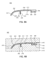
- FIG. 6A is a schematic cross-sectional view showing an antenna pattern frame according to another exemplary embodiment of the present invention.
- FIG. 6B is a schematic cross-sectional view showing a shape where the resin material is filled in a mould for manufacturing the antenna pattern frame in order to manufacture the antenna pattern frame of FIG. 6A ;
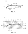
- FIG. 7A is a schematic cross-sectional view showing an antenna pattern frame according to another exemplary embodiment of the present invention.
- FIG. 7B is a schematic cross-sectional view showing a shape where a resin material is filled in a mould for manufacturing the antenna pattern frame in order to manufacture the antenna pattern frame of FIG. 7A ;
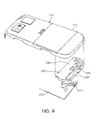
- FIG. 8 is an exploded perspective view of a case of an electronic device, a mobile communication terminal according to an exemplary embodiment of the present invention in which the antenna pattern radiator is embedded;
- FIG. 9 is a schematic diagram showing a method for manufacturing the case of the electronic device according to an exemplary embodiment of the present invention in which the antenna pattern radiator is embedded.
- FIGS. 10 to 13 are schematic cross-sectional views showing a process of inserting the antenna pattern radiator into the mould for manufacturing the electronic device and a shape where the resin material is filled in order to manufacture the case of the electronic device according to the first through fourth embodiments of the present invention.
- FIG. 1 is a perspective view schematically showing a partially cutaway case of an electronic device, a mobile communication terminal according to an exemplary embodiment of the present invention
- FIG. 2 is a perspective view schematically showing a radiator used in manufacturing an antenna pattern frame according to an exemplary embodiment of the present invention
- FIG. 3 is a perspective view schematically showing an antenna pattern frame according to an exemplary embodiment of the present invention
- FIG. 4 is a rear perspective view of the antenna pattern frame of FIG. 3 .
- a radiator 250 provided with an antenna pattern is embedded in a case 110 of a mobile communication terminal 100.
- an antenna pattern frame 200 that forms the radiator 250 provided with the antenna pattern on a radiator frame 230 is needed.
- the antenna pattern frame 200 may include the radiator 250 provided with an antenna pattern part 210, a connection terminal part 220, the radiator frame 230, and a guide boss 240.
- the radiator 250 is made of a conductive material such as aluminum, copper, or the like, to receive external signals and to transmit them to a signal processing unit in the electronic device such as the mobile communication terminal 100. Further, the radiator 250 may include the antenna pattern part 210 forming a meander line in order to receive the external signals of various bands.
- the radiator 250 in which the antenna pattern part 210 receiving the external signals and the connection terminal part 220 contacting a circuit substrate of the electronic device to transmit the external signals to the electronic device are disposed on a different plane may be provided.
- the radiator 250 may be formed to have a three-dimensional structure by bending the antenna pattern part 210 and the connection terminal part 220, respectively, and the antenna pattern part 210 and the connection terminal part 220 may be bent and connected to each other by a bending connection part 256.
- the bending connection part 256 may configure the antenna pattern part 210 and the connection terminal part 220 on a different plane and the connection terminal part 220 that is not embedded in the case of the electronic device may be exposed at an opposite surface 210b of the antenna pattern frame 200.
- the antenna pattern part 210 and the connection terminal part 220 are bent by the bending connection part 256, such that the radiator 250 may be implemented to have a three-dimensional curved shape.
- a radiator supporting part 258 may be protruded from the opposite surface 210b of the radiator frame 230.
- the radiator supporting part 258 may firmly support the connection terminal part 220 exposed to the opposite surface 210b and the bending connection part 256.
- the radiator 250 may be simultaneously formed with guide pin holes 252 or contact pin holes 254.
- the guide pin hole 252 and the contact pin hole 254 will be described below.
- connection terminal part 220 transmits the received external signals to the electronic device and may be formed by performing the bending, forming, and drawing processing on a part of the radiator 250.
- connection terminal part 220 may be manufactured to connect to the radiator 250 and may be connected to the terminal 210 of the circuit substrate 300.
- the radiator frame 230 may be a three-dimensional structure formed of a flat plane part 231 and a curve part 233 having a curvature.
- the radiator 250 may be flexible so that it is disposed at the curved part 233 of the radiator frame 230.
- the radiator frame 230 is an injection structure
- the antenna pattern part 210 may be formed on one surface 210a of the radiator frame 230
- the connection terminal part 220 may be formed on the opposite surface 210b of the one surface 210a.
- the radiator frame 230 may embed the antenna pattern in the case 110 of the electronic device by bonding the one surface 210a formed with the antenna pattern part 210 to the inside of the case 110 of the electronic device.
- the antenna pattern part 210 receiving the external signals and the connection terminal part 220 transmitting the external signals to the electronic device may be formed on a different plane.
- the guide boss 240 is formed to be protruded from the opposite surface of the one surface 210a formed with the antenna pattern part 210 of the radiator frame 230 and may be inserted in the manufacturing mould 500 (see FIG. 10 ) for injection-molding the case 120 of the electronic device.
- the guide boss 240 is inserted into the manufacturing mould 500 (see FIG. 10 ) such that it can be stably fixed on the mould, thereby making it possible to reduce the appearance defect and withstand the high injection pressure.
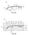
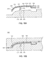
- FIG. 5A is a schematic cross-sectional view taken along line A-A of FIGS. 3 and 4
- FIG. 5B is a schematic cross-sectional view showing a shape where a resin material is filled in a mould for manufacturing the antenna pattern frame in order to manufacture the antenna pattern frame of FIG. 5A
- FIGS. 6A to 7B are cross-sectional views schematically showing another embodiment.
- the antenna pattern frame 200 may include the radiator 250 provided with the antenna pattern part 210, the connection terminal part 220, the radiator frame 230, and the guide boss 240.
- the radiator 250 may be simultaneously provided with the guide pin holes 252 or the contact pin holes 254 and is the same as the exemplary embodiment other than the guide pin hole 252 or the contact pin hole 254 and therefore, a description thereof will be described.
- the radiator 250 may be disposed with the guide pin 480 of the manufacturing mold 400 when performing the molding and may be formed with the guide pin holes 252 that prevent the motion of the radiator 250 on the radiator frame 230.
- the radiator 250 may be disposed with the contact pin 470 of the manufacturing mold 400 when performing the molding and may be formed with the contact pin holes 254 that prevent the motion of the radiator 250 on the radiator frame 230.
- the contact pin 470 and the guide pin 480 may be formed on the radiator 250 and the radiator frame 230 under the contact pin 470 is filled after performing the molding but the radiator frame 230 under the guide pin 480 is formed with holes.
- the contact pin 470 inserted into the contact pin hole 254 formed on the radiator 250, serves to prevent a horizontal movement of the radiator 250 in the mould 400 for manufacturing the antenna pattern frame 200.
- the guide pin 480 inserted into the guide pin hole 252 formed on the radiator 250 serves to prevent a vertical movement of the radiator 250 in the mould 400 for manufacturing the antenna pattern frame 200.
- the radiator 250 is disposed in the inner space 450 of the manufacturing mould 400 after providing the radiator 250.
- the inner space 450 is formed when an upper mould 420 and a lower mould 410 are combined with each other and the groove formed in the upper mould 420 or the lower mould 410 becomes the inner space 450 by the combination of the upper mould 420 and the lower mould 410.
- the radiator 250 may be fixed to the inner space 450 by passing or contacting the guide pin 480, the contact pin 470 or the guide pin 480 and the contact pin 470 that are formed in the upper or lower moulds 410 and 420, through and to the guide pin hole 252, the contact pin hole 254 or the guide pin hole 252 and the contact pin hole 254 that are formed in the antenna pattern part 210.
- the inner space 450 is filled with the resin material to form the radiator frame 230 that embeds the antenna pattern part 210 in the case 120 of the electronic device.
- the inner space 450 of the upper and lower moulds becomes the radiator frame 230 so that the antenna pattern part 210 is embedded in the case 120 of the electronic device to introduce the resin material into the inner space, thereby making it possible to form the resin material introducing part 440 in any one of the upper, lower or upper and lower moulds.
- the resin material is identically filled at the boundary surface between the radiator 250 and the radiator frame 230, such that the flowing of the resin material can be good when putting the radiator frame 230 in the mould for manufacturing the case 110 of the electronic device in which the antenna pattern is embedded and injection-molding the radiator frame 230.
- the inner space 450 of the upper or lower moulds 410 and 420 is formed with a curve part, such that the radiator frame 230 may have the curve part.
- the inner space 450 of the upper and lower moulds 410 and 420 may accommodate the connection terminal part 220 and include the radiator supporting part forming groove 460 to form the radiator supporting part 258 supporting the connection terminal part 220.
- the upper, lower or upper and lower moulds 410 and 420 may be provided with a compression pin 430 that compresses the connection terminal part 220 disposed in the radiator supporting part forming groove 460 to closely attach the connection terminal part 220 to the radiator supporting part forming groove 460.
- the compression pin 430 may prevent the resin material from being introduced under the connection terminal part 220 when the resin material is introduced.
- the electrical connection may be unstable, which can be prevented by the compression pin 430.
- the lower mould 410 may include a guide groove 490 so that the radiator frame 230 includes the guide boss 240 inserted into the manufacturing mould 400 for injection-molding the case 110 of the electronic device.
- the resin material is also introduced into the guide groove 490, such that the antenna pattern frame 200 may include the guide boss 240.
- the antenna pattern frame 200 may include a slot part 245 in the guide boss 240.
- the slot part 245 may be formed to include the protruding part corresponding to the slot part 245 in the guide groove 490 of the lower mould 410.
- the resin material introduced from the resin material introducing part 440 is filled in the guide groove 490 by the slot part 245 but is filled in the region other than the protruding part due to the protruding part.
- the guide boss 240 of the antenna pattern frame 200 includes the slot part 245 and the slot part 245 serves to elastically support and fix the manufacturing mould 400 when forming the case 110 of the electronic device.
- the antenna pattern frame 200 may include a small guide boss 240 as compared with the exemplary embodiment.
- the lower mould 410 may include the small guide groove 490 and the upper mould 420 may be formed with the protruding part 422 to form the introducing hole 260 that introduces the resin material into the inner space in the mould 500 (see FIG. 12 ) for manufacturing the case 110 of the electronic device in which the radiator 250 is embedded.
- the introduction of the resin material is prevented by the protruding part 422 and the antenna pattern frame 200 may be formed with holes.
- the protruding part 422 is to form the introducing hole 260 and is not limited to being formed in the upper mould 420. Therefore, the protruding part 422 may be formed in the lower mould 410.
- FIG. 8 is an exploded perspective view of the case of the electronic device, the mobile communication terminal according to an exemplary embodiment of the present invention in which the antenna pattern radiator is embedded.
- the case 120 of the electronic device according to the exemplary embodiment of the present invention in which the antenna pattern radiator 200 is embedded may include the radiator 250, the radiator frame 230, and the case frame 120.
- the radiator 250 and the radiator frame 230 are described in the exemplary embodiment and therefore, a description thereof will be omitted.
- the case frame 120 covers one surface of the radiator frame 230 in which the antenna pattern part 210 is formed to embed the antenna pattern part 210 between the radiator frames 230.
- radiator frame 230 and the case frame 120 may be integrated without a clearly defined boundary therebetween.
- the antenna pattern part 210 may not be shown and only the connection terminal part 220 may be shown.
- the radiator frame 230, the case frame 120, or the radiator frame 230 and the case frame 120 may be formed by the injection molding.
- the radiator frame 230 and the case frame 120 are formed of a separate injection fixture, the case 120 of the electronic device is manufactured by bonding the radiator frame 230 in which the radiator 250 is formed to the case frame 120.
- the case frame 120 is injection-molded in the radiator frame 230, such that it may be subjected to a double injection molding.
- the radiator frame 230 is disposed in the mould and is then subjected to insert injection, thereby making it possible to integrate the radiator frame 230 and the case frame 120.
- the guide pin hole 252 or the contact pin hole 254 formed in the radiator frame 230 is disposed in the mould 500 (see FIG. 10 ) for manufacturing the case of the electronic device, they are combined with the guide pin or the contact pin (not shown) formed in the manufacturing mould 500, thereby making it possible to prevent the antenna pattern frame 200 from moving in the manufacturing mould 500.
- FIG. 9 is a schematic diagram showing a method for manufacturing the case of the electronic device according to an exemplary embodiment of the present invention in which the antenna pattern radiator is embedded.
- the case frame 120 is a separate injection product having a radiator receiving groove 115 in a shape corresponding to the radiator frame 230 and the case 110 of the electronic device in which the antenna pattern radiator is embedded by bonding the radiator frame 230 to the radiator receiving groove 115 may be manufactured.
- An adhesive layer 495 is formed on the surface of the radiator 250 of the antenna pattern frame 200.
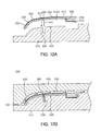
- FIGS. 10 through 13 are schematic cross-sectional views showing a process of inserting the antenna pattern radiator into the mould for manufacturing the electronic device and a shape where the resin material is filled in order to manufacture the case of the electronic device according to the first through fourth embodiments of the present invention.
- the guide boss 240 of the antenna pattern frame 200 is fixed and supported by being inserted into the guide groove 530 of the lower mould 510.
- the radiator frame 230 is disposed in the mould 500 for manufacturing the case of the electronic device having an inner space 540 accommodating the radiator frame 230 and the resin material is introduced into the mould, such that the radiator frame 230 is integrated with the case 110 of the electronic device.
- radiator frame 230 and the case frame 120 may be formed without a clearly defined boundary therebetween.
- the antenna pattern frame 200 may be fixed and supported not to move by the guide boss 240 and the guide groove 530 in the secondary injection manufacturing mould 500, even in the secondary injection as in the primary injection.
- the guide boss 240 is inserted into the secondary injection mould 500 to serve to fix and support the injection product, that is, the radiator frame 230 so that the injection product can withstand the high temperature and the high injection pressure.
- the inner space 540 of the manufacturing mould 500 may include the curve forming part 525 so that the case 110 of the electronic device has the curve part.
- the mould 500 for manufacturing the case of the electronic device that manufactures the case 120 of the electronic device in which the antenna pattern is embedded by the secondary injection may form the antenna pattern part 210 receiving the external signals and the connection terminal part 220 contacting the circuit substrate of the electronic device on a different plane.
- the radiator frame 230 having the radiator 250 is formed in the upper or lower moulds 510 and 520 and the upper and lower moulds 510 and 520 of the mould for manufacturing the case of the electronic device and when the upper or lower moulds 510 and 520 are combined with each other, the case of the electronic device may include the resin material introducing part 530 introducing the resin material into the inner space so that the inner space 540 formed in the mould becomes the case 120 of the electronic device.
- the radiator frame 230 is provided with the guide pin hole or the contact pin hole, wherein the guide pin hole or the contacting hole may be fixed to the guide pin or the contact pin formed in the manufacturing mould 500 . This is to prevent the radiator frame 230 from moving in the manufacturing mould.
- the guide boss 240 can be easily inserted into the guide groove 530 of the lower mould 510 by the slot part 245 in the guide boss 240 of the antenna pattern frame 200 and then, be fixed and supported to the outside of the slot part 245 by its elasticity.
- the guide boss 240 has a structure capable of withstanding high injection pressure.
- the guide boss 240 of the antenna pattern frame 200 is inserted into the guide groove 530 of the lower mould 510 and then, a space may be formed in a predetermined area of the guide groove 530.
- the resin material is introduced into the resin inlet 530, such that it is introduced into the introducing hole 260 of the antenna pattern frame 200. Thereafter, the resin material may also be filled in the space of the guide groove 530.
- the guide boss since the antenna pattern frame 200 is fixed and supported by the flowing of the resin material, the guide boss has a structure capable of withstanding the injection pressure.
- the guide groove 530 includes a guide boss receiving part to fix and support the guide boss 240 and the guide boss receiving part may include a variable part 532 having a diameter larger than that of the guide boss 240 and a fixing part 534 having a diameter smaller than that of the variable part 532.
- variable part 532 receives the guide boss 240 by being protruded to the upper portion of the lower mould before the guide boss 240 is inserted and then, is inserted into the guide groove 530 of the lower mould, such that the antenna pattern frame 200 is fixed and supported to the lower mould 510.
- the antenna pattern frame 200 may be easily fixed to the lower mould 510 by the guide boss receiving part 530 configured of the variable part 532 and the fixing part 534 and can withstand high-temperature and high-pressure injection liquid.
- the antenna pattern frame, the case of the electronic device, and the mould for manufacturing the same stably fixes the antenna pattern frame to the inner space of the mould for manufacturing the case of the electronic device when molding the case of the electronic device in which the antenna radiator is embedded, thereby making it possible to reduce the appearance defect and to provide a structure withstanding the high-temperature and high-pressure injection liquid when performing the injection molding.
Abstract
Description
- This application claims the priority of
Korean Patent Application No. 10-2010-0017246 filed on February 25, 2010 - The present invention relates to an antenna pattern frame, a case of an electronic device, and a mould for manufacturing the same, and more particularly, to an antenna pattern frame having an antenna radiator formed on the surface thereof so that the antenna radiator is embedded in a case of an electronic device, a case of an electronic device, and a mould for manufacturing the same.
- Mobile communication terminals, for example, cellular phones, PDAs, navigation devices, notebook computers, or the like, that are used to support wireless communication are necessities in modern society. Mobile communication terminals are being developed to have functions, such as CDMA, wireless LAN, GSM, DMB, or the like. One of the most important parts that enable these functions is an antenna.
- The antenna used in the mobile communication terminal has devolved from an exterior type antenna such as a rod antenna or a helical antenna to an interior type antenna where an antenna is mounted in the terminal.
- There have, however, been problems, in that the exterior type antenna is vulnerable to external impacts and the interior type antenna increases the volume of the terminal.
- In order to solve the problems, a research to integrate the mobile communication terminal and the antenna has been actively conducted.
- An aspect of the present invention provides an antenna pattern frame having an antenna radiator formed on the surface thereof and a case of an electronic device in which the antenna radiator is embedded.
- Another aspect of the present invention provides a mould for manufacturing an antenna pattern frame and a case of an electronic device in which an antenna radiator is embedded.
- Another aspect of the present invention reduces an appearance defect by stably fixing an antenna pattern frame to a mould for manufacturing a case of an electronic device when molding the case of the electronic device in which an antenna radiator is embedded.
- According to an aspect of the present invention, there is provided an antenna pattern frame, including: a radiator that includes an antenna pattern part transmitting and receiving signals and a connection terminal part transmitting and receiving the signals to and from a circuit substrate of an electronic device; and a radiator frame that embeds the antenna pattern part in a case of the electronic device and supports the radiator, the radiator being manufactured by injection molding, wherein the radiator frame forms a guide boss inserted into a manufacturing mould for injection-molding the case of the electronic device in which the radiator is embedded.
- The guide boss may include a slot part therein so that it is elastically supported and fixed to the manufacturing mould.
- The radiator frame includes an introducing hole formed to introduce a resin material when injection-molding the case of the electronic device.
- The radiator may include a connection part that is a part of the radiator and connects the antenna pattern part to the connection terminal part, and the connection part may be formed so that the antenna pattern part is formed on one surface of the radiator frame and the connection terminal part is formed on an opposite surface to the one surface.
- The connection terminal part may contact and support the radiator supporting part that is protruded from the opposite surface of the one surface on which the antenna pattern part of the radiator frame is formed.
- According to another aspect of the present invention, there is provided a case of an electronic device, including: a radiator that includes an antenna pattern part transmitting and receiving signals and a connection terminal part transmitting and receiving the signals to and from a circuit substrate of an electronic device; a radiator frame including a guide boss that supports and fixes the radiator and is inserted in the manufacturing mould for injection-molding the case of the electronic device in which the radiator is embedded, the radiator being manufactured by injection molding; and a case frame that covers one surface of the radiator frame to embed the antenna pattern part between the radiator frames.
- The guide boss may include a slot part so that it is elastically supported and fixed to the manufacturing mould.
- The radiator frame may include an introducing hole formed to introduce a resin material when injection-molding the case of the electronic device.
- The introducing hole may be formed to integrate a resin material introduced through the introducing hole with the guide boss.
- The connection part may be formed so that the antenna pattern part is formed on one surface of the radiator frame and the connection terminal part may be formed on an opposite surface to the one surface.
- The connection terminal part may contact and support the radiator supporting part that is protruded from the opposite surface of the one surface on which the antenna pattern part of the radiator frame is formed.
- According to another aspect of the present invention, there is provided a mould for manufacturing an antenna pattern frame, including: upper and lower moulds receiving a radiator that includes an antenna pattern part transmitting and receiving signals, a connection terminal part connected to a circuit substrate of an electronic device, and a connection part connecting the antenna pattern part to the connection terminal parts; and when the upper and lower moulds are combined with each other, a resin material introducing part formed in any one of the upper, lower, or upper and lower moulds to introduce a resin material into an inner space so that the inner space of the upper and lower moulds becomes the radiator frame to embed the antenna pattern part in the case of the electronic device, wherein the lower mould includes a guide groove so that the radiator frame includes a guide boss that is inserted into the manufacturing mould for injection-molding the case of the electronic device and the radiator is the radiator frame by the inner space.
- The lower mould may include a protruding part corresponding to the slot part in the guide groove to form a slot part in the guide boss.
- Any one of the upper, lower, or upper and lower moulds may include an interrupting boss that prevents the resin material from being introduced in order to form an introducing hole for introducing the resin material on the antenna pattern frame when the case of the electronic device is injection-molded.
- The inner space of the upper and lower moulds may receive the connection terminal part and may include a radiator supporting part forming groove in order to form the radiator supporting part supporting the connection terminal part.
- Any one of the upper, lower or upper and lower moulds may be provided with a compression pin that compresses the connection terminal part disposed in the radiator supporting part forming groove.
- According to another aspect of the present invention, there is provided a mould for manufacturing a case of an electronic device, including: upper and lower moulds that receive a radiator including an antenna pattern part transmitting or receiving signals, a radiator including a connection terminal part contacting a circuit substrate of an electronic device, a radiator frame supporting the radiator, and an antenna pattern frame including a guide boss formed to be protruded from one surface of the radiator frame; when the upper and lower moulds are combined with each other, a resin material introducing part formed in any one of the upper, lower, or upper and lower moulds to form a case of an electronic device by combining the antenna pattern frame with the resin material due to the introduction of the resin material in the inner space of the upper and lower moulds; and wherein the lower mould includes a guide groove formed to insert the guide boss and the antenna pattern frame is the case of the electronic device by the inner space.
- The guide groove may include the guide boss receiving part to fix and support the guide boss.
- The guide boss receiving part is configured of a variable part having a diameter larger than that of the guide boss and a fixing part having a diameter smaller than that of the variable part.
- The variable part may receive the guide boss by being protruded to the upper portion of the lower mould before the guide boss is inserted, and may be inserted into the guide groove of the lower mould after the guide boss is received.
- The above and other aspects, features and other advantages of the present invention will be more clearly understood from the following detailed description taken in conjunction with the accompanying drawings, in which:
-
FIG. 1 is a perspective view schematically showing a partially cutaway case of an electronic device, a mobile communication terminal according to an exemplary embodiment of the present invention; -
FIG. 2 is a perspective view schematically showing a radiator used in manufacturing an antenna pattern frame according to an exemplary embodiment of the present invention; -
FIG. 3 is a perspective view schematically showing an antenna pattern frame according to an exemplary embodiment of the present invention; -
FIG. 4 is a rear perspective view of the antenna pattern frame ofFIG. 3 ; -
FIG. 5A is a schematic cross-sectional view taken along line A-A ofFIGS. 3 and4 ; -
FIG. 5B is a schematic cross-sectional view showing a shape where a resin material is filled in a mould for manufacturing the antenna pattern frame in order to manufacture the antenna pattern frame ofFIG. 5A ; -
FIG. 6A is a schematic cross-sectional view showing an antenna pattern frame according to another exemplary embodiment of the present invention; -
FIG. 6B is a schematic cross-sectional view showing a shape where the resin material is filled in a mould for manufacturing the antenna pattern frame in order to manufacture the antenna pattern frame ofFIG. 6A ; -
FIG. 7A is a schematic cross-sectional view showing an antenna pattern frame according to another exemplary embodiment of the present invention; -
FIG. 7B is a schematic cross-sectional view showing a shape where a resin material is filled in a mould for manufacturing the antenna pattern frame in order to manufacture the antenna pattern frame ofFIG. 7A ; -
FIG. 8 is an exploded perspective view of a case of an electronic device, a mobile communication terminal according to an exemplary embodiment of the present invention in which the antenna pattern radiator is embedded; -
FIG. 9 is a schematic diagram showing a method for manufacturing the case of the electronic device according to an exemplary embodiment of the present invention in which the antenna pattern radiator is embedded; and -
FIGS. 10 to 13 are schematic cross-sectional views showing a process of inserting the antenna pattern radiator into the mould for manufacturing the electronic device and a shape where the resin material is filled in order to manufacture the case of the electronic device according to the first through fourth embodiments of the present invention. - Exemplary embodiments of the present invention will now be described in detail with reference to the accompanying drawings. However, it should be noted that the spirit of the present invention is not limited to the embodiments set forth herein and those skilled in the art and understanding the present invention can easily accomplish retrogressive inventions or other embodiments included in the spirit of the present invention by the addition, modification, and removal of components within the same spirit, but those are construed as being included in the spirit of the present invention.
- Further, throughout the drawings, the same or similar reference numerals will be used to designate the same components or like components having the same functions in the scope of the similar idea.
-
FIG. 1 is a perspective view schematically showing a partially cutaway case of an electronic device, a mobile communication terminal according to an exemplary embodiment of the present invention,FIG. 2 is a perspective view schematically showing a radiator used in manufacturing an antenna pattern frame according to an exemplary embodiment of the present invention,FIG. 3 is a perspective view schematically showing an antenna pattern frame according to an exemplary embodiment of the present invention, andFIG. 4 is a rear perspective view of the antenna pattern frame ofFIG. 3 . - Referring to
FIGS. 1 through 4 , it can be appreciated that aradiator 250 provided with an antenna pattern according to an exemplary embodiment of the present invention is embedded in acase 110 of amobile communication terminal 100. In order to form theradiator 250 provided with the antenna pattern in the inside of thecase 110, anantenna pattern frame 200 that forms theradiator 250 provided with the antenna pattern on aradiator frame 230 is needed. - The
antenna pattern frame 200 according to an exemplary embodiment of the present invention may include theradiator 250 provided with anantenna pattern part 210, aconnection terminal part 220, theradiator frame 230, and aguide boss 240. - The
radiator 250 is made of a conductive material such as aluminum, copper, or the like, to receive external signals and to transmit them to a signal processing unit in the electronic device such as themobile communication terminal 100. Further, theradiator 250 may include theantenna pattern part 210 forming a meander line in order to receive the external signals of various bands. - The
radiator 250 in which theantenna pattern part 210 receiving the external signals and theconnection terminal part 220 contacting a circuit substrate of the electronic device to transmit the external signals to the electronic device are disposed on a different plane may be provided. - Further, the
radiator 250 may be formed to have a three-dimensional structure by bending theantenna pattern part 210 and theconnection terminal part 220, respectively, and theantenna pattern part 210 and theconnection terminal part 220 may be bent and connected to each other by abending connection part 256. - The
bending connection part 256 may configure theantenna pattern part 210 and theconnection terminal part 220 on a different plane and theconnection terminal part 220 that is not embedded in the case of the electronic device may be exposed at anopposite surface 210b of theantenna pattern frame 200. - In other words, the
antenna pattern part 210 and theconnection terminal part 220 are bent by thebending connection part 256, such that theradiator 250 may be implemented to have a three-dimensional curved shape. - In order to support the
radiator 250 having the three-dimensional curved shape, aradiator supporting part 258 may be protruded from theopposite surface 210b of theradiator frame 230. - The
radiator supporting part 258 may firmly support theconnection terminal part 220 exposed to theopposite surface 210b and thebending connection part 256. - The
radiator 250 may be simultaneously formed with guide pin holes 252 or contact pin holes 254. - The
guide pin hole 252 and thecontact pin hole 254 will be described below. - The
connection terminal part 220 transmits the received external signals to the electronic device and may be formed by performing the bending, forming, and drawing processing on a part of theradiator 250. - In addition, after the
connection terminal part 220 is separately manufactured from theradiator 250, it may be manufactured to connect to theradiator 250 and may be connected to theterminal 210 of thecircuit substrate 300. - Meanwhile, the
radiator frame 230 may be a three-dimensional structure formed of aflat plane part 231 and acurve part 233 having a curvature. Theradiator 250 may be flexible so that it is disposed at thecurved part 233 of theradiator frame 230. - The
radiator frame 230 is an injection structure, theantenna pattern part 210 may be formed on onesurface 210a of theradiator frame 230, and theconnection terminal part 220 may be formed on theopposite surface 210b of the onesurface 210a. - The
radiator frame 230 may embed the antenna pattern in thecase 110 of the electronic device by bonding the onesurface 210a formed with theantenna pattern part 210 to the inside of thecase 110 of the electronic device. - In the structure of the
radiator 250 embedded in thecase 110 of the electronic device, theantenna pattern part 210 receiving the external signals and theconnection terminal part 220 transmitting the external signals to the electronic device may be formed on a different plane. - The
guide boss 240 is formed to be protruded from the opposite surface of the onesurface 210a formed with theantenna pattern part 210 of theradiator frame 230 and may be inserted in the manufacturing mould 500 (seeFIG. 10 ) for injection-molding thecase 120 of the electronic device. - The
guide boss 240 is inserted into the manufacturing mould 500 (seeFIG. 10 ) such that it can be stably fixed on the mould, thereby making it possible to reduce the appearance defect and withstand the high injection pressure. -
FIG. 5A is a schematic cross-sectional view taken along line A-A ofFIGS. 3 and4 ,FIG. 5B is a schematic cross-sectional view showing a shape where a resin material is filled in a mould for manufacturing the antenna pattern frame in order to manufacture the antenna pattern frame ofFIG. 5A , andFIGS. 6A to 7B are cross-sectional views schematically showing another embodiment. - Referring to
FIG. 5A , theantenna pattern frame 200 according to an exemplary embodiment of the present invention may include theradiator 250 provided with theantenna pattern part 210, theconnection terminal part 220, theradiator frame 230, and theguide boss 240. - The
radiator 250 may be simultaneously provided with the guide pin holes 252 or the contact pin holes 254 and is the same as the exemplary embodiment other than theguide pin hole 252 or thecontact pin hole 254 and therefore, a description thereof will be described. - The
radiator 250 may be disposed with theguide pin 480 of themanufacturing mold 400 when performing the molding and may be formed with the guide pin holes 252 that prevent the motion of theradiator 250 on theradiator frame 230. - In addition, the
radiator 250 may be disposed with thecontact pin 470 of themanufacturing mold 400 when performing the molding and may be formed with the contact pin holes 254 that prevent the motion of theradiator 250 on theradiator frame 230. - The
contact pin 470 and theguide pin 480 may be formed on theradiator 250 and theradiator frame 230 under thecontact pin 470 is filled after performing the molding but theradiator frame 230 under theguide pin 480 is formed with holes. - The
contact pin 470, inserted into thecontact pin hole 254 formed on theradiator 250, serves to prevent a horizontal movement of theradiator 250 in themould 400 for manufacturing theantenna pattern frame 200. - Further, the
guide pin 480 inserted into theguide pin hole 252 formed on theradiator 250 serves to prevent a vertical movement of theradiator 250 in themould 400 for manufacturing theantenna pattern frame 200. - Referring to
FIG. 5B , theradiator 250 is disposed in theinner space 450 of themanufacturing mould 400 after providing theradiator 250. - The
inner space 450 is formed when anupper mould 420 and alower mould 410 are combined with each other and the groove formed in theupper mould 420 or thelower mould 410 becomes theinner space 450 by the combination of theupper mould 420 and thelower mould 410. - When the
upper mould 420 and thelower mould 410 are combined with each other, theradiator 250 may be fixed to theinner space 450 by passing or contacting theguide pin 480, thecontact pin 470 or theguide pin 480 and thecontact pin 470 that are formed in the upper orlower moulds guide pin hole 252, thecontact pin hole 254 or theguide pin hole 252 and thecontact pin hole 254 that are formed in theantenna pattern part 210. - The
inner space 450 is filled with the resin material to form theradiator frame 230 that embeds theantenna pattern part 210 in thecase 120 of the electronic device. - When the upper and lower moulds are combined with each other, the
inner space 450 of the upper and lower moulds becomes theradiator frame 230 so that theantenna pattern part 210 is embedded in thecase 120 of the electronic device to introduce the resin material into the inner space, thereby making it possible to form the resinmaterial introducing part 440 in any one of the upper, lower or upper and lower moulds. - The resin material is identically filled at the boundary surface between the
radiator 250 and theradiator frame 230, such that the flowing of the resin material can be good when putting theradiator frame 230 in the mould for manufacturing thecase 110 of the electronic device in which the antenna pattern is embedded and injection-molding theradiator frame 230. - At this time, the
inner space 450 of the upper orlower moulds radiator frame 230 may have the curve part. - Further, the
inner space 450 of the upper andlower moulds connection terminal part 220 and include the radiator supportingpart forming groove 460 to form theradiator supporting part 258 supporting theconnection terminal part 220. - In addition, the upper, lower or upper and
lower moulds compression pin 430 that compresses theconnection terminal part 220 disposed in the radiator supportingpart forming groove 460 to closely attach theconnection terminal part 220 to the radiator supportingpart forming groove 460. - The
compression pin 430 may prevent the resin material from being introduced under theconnection terminal part 220 when the resin material is introduced. When the injection material is covered on a part of theconnection terminal part 220, the electrical connection may be unstable, which can be prevented by thecompression pin 430. - Further, the
lower mould 410 may include aguide groove 490 so that theradiator frame 230 includes theguide boss 240 inserted into themanufacturing mould 400 for injection-molding thecase 110 of the electronic device. - The resin material is also introduced into the
guide groove 490, such that theantenna pattern frame 200 may include theguide boss 240. - Referring to
FIGS. 6A and 6B , theantenna pattern frame 200 according to another embodiment of the present invention may include aslot part 245 in theguide boss 240. - The
slot part 245 may be formed to include the protruding part corresponding to theslot part 245 in theguide groove 490 of thelower mould 410. - The resin material introduced from the resin
material introducing part 440 is filled in theguide groove 490 by theslot part 245 but is filled in the region other than the protruding part due to the protruding part. - Therefore, the
guide boss 240 of theantenna pattern frame 200 includes theslot part 245 and theslot part 245 serves to elastically support and fix themanufacturing mould 400 when forming thecase 110 of the electronic device. - Referring to
FIGS. 7A and 7B , theantenna pattern frame 200 according to another embodiment of the present invention may include asmall guide boss 240 as compared with the exemplary embodiment. - In order to form the
guide boss 240, thelower mould 410 may include thesmall guide groove 490 and theupper mould 420 may be formed with theprotruding part 422 to form the introducinghole 260 that introduces the resin material into the inner space in the mould 500 (seeFIG. 12 ) for manufacturing thecase 110 of the electronic device in which theradiator 250 is embedded. - The introduction of the resin material is prevented by the protruding
part 422 and theantenna pattern frame 200 may be formed with holes. - However, it is to be noted that the
protruding part 422 is to form the introducinghole 260 and is not limited to being formed in theupper mould 420. Therefore, the protrudingpart 422 may be formed in thelower mould 410. -
FIG. 8 is an exploded perspective view of the case of the electronic device, the mobile communication terminal according to an exemplary embodiment of the present invention in which the antenna pattern radiator is embedded. - The
case 120 of the electronic device according to the exemplary embodiment of the present invention in which theantenna pattern radiator 200 is embedded may include theradiator 250, theradiator frame 230, and thecase frame 120. - The
radiator 250 and theradiator frame 230 are described in the exemplary embodiment and therefore, a description thereof will be omitted. - The
case frame 120 covers one surface of theradiator frame 230 in which theantenna pattern part 210 is formed to embed theantenna pattern part 210 between the radiator frames 230. - Further, the
radiator frame 230 and thecase frame 120 may be integrated without a clearly defined boundary therebetween. When viewing thecase 110 of the electronic device from the rear, theantenna pattern part 210 may not be shown and only theconnection terminal part 220 may be shown. - The
radiator frame 230, thecase frame 120, or theradiator frame 230 and thecase frame 120 may be formed by the injection molding. In particular, when theradiator frame 230 and thecase frame 120 are formed of a separate injection fixture, thecase 120 of the electronic device is manufactured by bonding theradiator frame 230 in which theradiator 250 is formed to thecase frame 120. - Meanwhile, the
case frame 120 is injection-molded in theradiator frame 230, such that it may be subjected to a double injection molding. In other words, theradiator frame 230 is disposed in the mould and is then subjected to insert injection, thereby making it possible to integrate theradiator frame 230 and thecase frame 120. - When the
guide pin hole 252 or thecontact pin hole 254 formed in theradiator frame 230 is disposed in the mould 500 (seeFIG. 10 ) for manufacturing the case of the electronic device, they are combined with the guide pin or the contact pin (not shown) formed in themanufacturing mould 500, thereby making it possible to prevent theantenna pattern frame 200 from moving in themanufacturing mould 500. -
FIG. 9 is a schematic diagram showing a method for manufacturing the case of the electronic device according to an exemplary embodiment of the present invention in which the antenna pattern radiator is embedded. - Referring to
FIG. 9 , thecase frame 120 is a separate injection product having aradiator receiving groove 115 in a shape corresponding to theradiator frame 230 and thecase 110 of the electronic device in which the antenna pattern radiator is embedded by bonding theradiator frame 230 to theradiator receiving groove 115 may be manufactured. - An
adhesive layer 495 is formed on the surface of theradiator 250 of theantenna pattern frame 200. -
FIGS. 10 through 13 are schematic cross-sectional views showing a process of inserting the antenna pattern radiator into the mould for manufacturing the electronic device and a shape where the resin material is filled in order to manufacture the case of the electronic device according to the first through fourth embodiments of the present invention. - Referring to
FIG. 10 , theguide boss 240 of theantenna pattern frame 200 is fixed and supported by being inserted into theguide groove 530 of thelower mould 510. - The
radiator frame 230 is disposed in themould 500 for manufacturing the case of the electronic device having aninner space 540 accommodating theradiator frame 230 and the resin material is introduced into the mould, such that theradiator frame 230 is integrated with thecase 110 of the electronic device. - Meanwhile, the
radiator frame 230 and thecase frame 120 may be formed without a clearly defined boundary therebetween. - When the injection of the
antenna pattern frame 200 is called the primary injection and the injection of thecase 110 of the electronic device is called the secondary injection, theantenna pattern frame 200 may be fixed and supported not to move by theguide boss 240 and theguide groove 530 in the secondaryinjection manufacturing mould 500, even in the secondary injection as in the primary injection. - In other words, the
guide boss 240 is inserted into thesecondary injection mould 500 to serve to fix and support the injection product, that is, theradiator frame 230 so that the injection product can withstand the high temperature and the high injection pressure. - Further, the
inner space 540 of themanufacturing mould 500 may include thecurve forming part 525 so that thecase 110 of the electronic device has the curve part. - Meanwhile, the
mould 500 for manufacturing the case of the electronic device that manufactures thecase 120 of the electronic device in which the antenna pattern is embedded by the secondary injection may form theantenna pattern part 210 receiving the external signals and theconnection terminal part 220 contacting the circuit substrate of the electronic device on a different plane. - The
radiator frame 230 having theradiator 250 is formed in the upper orlower moulds lower moulds lower moulds material introducing part 530 introducing the resin material into the inner space so that theinner space 540 formed in the mould becomes thecase 120 of the electronic device. - Similar to the
radiator 250, theradiator frame 230 is provided with the guide pin hole or the contact pin hole, wherein the guide pin hole or the contacting hole may be fixed to the guide pin or the contact pin formed in themanufacturing mould 500 . This is to prevent theradiator frame 230 from moving in the manufacturing mould. - Referring to
FIG. 11 , theguide boss 240 can be easily inserted into theguide groove 530 of thelower mould 510 by theslot part 245 in theguide boss 240 of theantenna pattern frame 200 and then, be fixed and supported to the outside of theslot part 245 by its elasticity. As a result, theguide boss 240 has a structure capable of withstanding high injection pressure. - Referring to
FIG. 12 , theguide boss 240 of theantenna pattern frame 200 is inserted into theguide groove 530 of thelower mould 510 and then, a space may be formed in a predetermined area of theguide groove 530. - The resin material is introduced into the
resin inlet 530, such that it is introduced into the introducinghole 260 of theantenna pattern frame 200. Thereafter, the resin material may also be filled in the space of theguide groove 530. - In this case, since the
antenna pattern frame 200 is fixed and supported by the flowing of the resin material, the guide boss has a structure capable of withstanding the injection pressure. - Referring to
FIG. 13 , theguide groove 530 includes a guide boss receiving part to fix and support theguide boss 240 and the guide boss receiving part may include avariable part 532 having a diameter larger than that of theguide boss 240 and a fixingpart 534 having a diameter smaller than that of thevariable part 532. - The
variable part 532 receives theguide boss 240 by being protruded to the upper portion of the lower mould before theguide boss 240 is inserted and then, is inserted into theguide groove 530 of the lower mould, such that theantenna pattern frame 200 is fixed and supported to thelower mould 510. - Therefore, the
antenna pattern frame 200 may be easily fixed to thelower mould 510 by the guideboss receiving part 530 configured of thevariable part 532 and the fixingpart 534 and can withstand high-temperature and high-pressure injection liquid. - As set forth above, the antenna pattern frame, the case of the electronic device, and the mould for manufacturing the same according to the present invention stably fixes the antenna pattern frame to the inner space of the mould for manufacturing the case of the electronic device when molding the case of the electronic device in which the antenna radiator is embedded, thereby making it possible to reduce the appearance defect and to provide a structure withstanding the high-temperature and high-pressure injection liquid when performing the injection molding.
- While the present invention has been shown and described in connection with the exemplary embodiments, it will be apparent to those skilled in the art that modifications and variations can be made without departing from the spirit and scope of the invention as defined by the appended claims.
Claims (20)
- An antenna pattern frame, comprising:a radiator that includes an antenna pattern part transmitting and receiving signals and a connection terminal part transmitting and receiving the signals to and from a circuit substrate of an electronic device; anda radiator frame that embeds the antenna pattern part in a case of the electronic device and supports the radiator, the radiator being manufactured by injection molding,wherein the radiator frame forms a guide boss inserted into a manufacturing mould for injection-molding the case of the electronic device in which the radiator is embedded.
- The antenna pattern frame of claim 1, wherein the guide boss includes a slot part therein so that it is elastically supported and fixed to the manufacturing mould.
- The antenna pattern frame of claim 1, wherein the radiator frame includes an introducing hole formed to introduce a resin material when injection-molding the case of the electronic device.
- The antenna pattern frame of claim 1, wherein the radiator includes a connection part that is a part of the radiator and connects the antenna pattern part to the connection terminal part, and
the connection part is formed so that the antenna pattern part is formed on one surface of the radiator frame and the connection terminal part is formed on an opposite surface to the one surface. - The antenna pattern frame of claim 1, wherein the connection terminal part contacts and supports the radiator supporting part that is protruded from the opposite surface of the one surface on which the antenna pattern part of the radiator frame is formed.
- A case of an electronic device, comprising:a radiator that includes an antenna pattern part transmitting and receiving signals and a connection terminal part transmitting and receiving the signals to and from a circuit substrate of an electronic device;a radiator frame including a guide boss that supports and fixes the radiator and is inserted in the manufacturing mould for inj ection-molding the case of the electronic device in which the radiator is embedded, the radiator being manufactured by injection molding; anda case frame that covers one surface of the radiator frame to embed the antennat pattern part between the radiator frames.
- The case of the electronic device of claim 6, wherein the guide boss includes a slot part so that it is elastically supported and fixed to the manufacturing mould.
- The case of the electronic device of claim 6, wherein the radiator frame includes an introducing hole formed to introduce a resin material when injection-molding the case of the electronic device.
- The case of the electronic device of claim 8, wherein the introducing hole is formed to integrate a resin material introduced through the introducing hole with the guide boss.
- The case of the electronic device of claim 6, wherein the connection part is formed so that the antenna pattern part is formed on one surface of the radiator frame and the connection terminal part is formed on an opposite surface to the one surface.
- The case of the electronic device of claim 6, wherein the connection terminal part contacts and supports the radiator supporting part that is protruded from the opposite surface of the one surface on which the antenna pattern part of the radiator frame is formed.
- A mould for manufacturing an antenna pattern frame, comprising:upper and lower moulds receiving a radiator that includes an antenna pattern part transmitting and receiving signals, a connection terminal part connected to a circuit substrate of an electronic device, and a connection part connecting the antenna pattern part to the connection terminal part; andwhen the upper and lower moulds are combined with each other, a resin material introducing part formed in any one of the upper, lower, or upper and lower moulds to introduce a resin material into an inner space so that the inner space of the upper and lower moulds becomes the radiator frame to embed the antenna pattern part in the case of the electronic device,
wherein the lower mould includes a guide groove so that the radiator frame includes a guide boss that is inserted into the manufacturing mould for injection-molding the case of the electronic device and the radiator is the radiator frame by the inner space. - The mould for manufacturing an antenna pattern frame of claim 12, wherein the lower mould includes a protruding part corresponding to the slot part in the guide groove to form a slot part in the guide boss.
- The mould for manufacturing an antenna pattern frame of claim 12, wherein any one of the upper, lower, or upper and lower moulds includes an interrupting boss that prevents the resin material from being introduced in order to form an introducing hole for introducing the resin material on the antenna pattern frame when the case of the electronic device is injection-molded.
- The mould for manufacturing an antenna pattern frame of claim 12, wherein the inner space of the upper and lower moulds receives the connection terminal part and includes a radiator supporting part forming groove in order to form the radiator supporting part supporting the connection terminal part.
- The mould for manufacturing an antenna pattern frame of claim 12, wherein any one of the upper, lower or upper and lower moulds is provided with a compression pin that compresses the connection terminal part disposed in the radiator supporting part forming groove.
- A mould for manufacturing a case of an electronic device, comprising:upper and lower moulds that receive a radiator including an antenna pattern part transmitting or receiving signals, a radiator including a connection terminal part contacting a circuit substrate of an electronic device, a radiator frame supporting the radiator, and an antenna pattern frame including a guide boss formed to be protruded from one surface of the radiator frame; andwhen the upper and lower moulds are combined with each other, a resin material introduing part formed in any one of the upper, lower, or upper and lower moulds to form a case of an electronic device by combining the antenna pattern frame with the resin material due to the introduction of the resin material in the inner space of the upper and lower moulds;wherein the lower mould includes a guide groove formed to insert the guide boss and the antenna pattern frame is the case of the electronic device by the inner space.
- The mould for manufacturing the case of the electronic device of claim 17, wherein the guide groove includes the guide boss receiving part to fix and support the guide boss.
- The mould for manufacturing the case of the electronic device of claim 18, wherein the guide boss receiving part is configured of a variable part having a diameter larger than that of the guide boss and a fixing part having a diameter smaller than that of the variable part.
- The mould for manufacturing the case of the electronic device of claim 19, wherein the variable part receives the guide boss by being protruded to the upper portion of the lower mould before the guide boss is inserted, and is inserted into the guide groove of the lower mould after the guide boss is received.
Applications Claiming Priority (1)
| Application Number | Priority Date | Filing Date | Title |
|---|---|---|---|
| KR1020100017246A KR101101491B1 (en) | 2010-02-25 | 2010-02-25 | Antenna pattern frame, case of electronic device and mould for manufacturing the same |
Publications (2)
| Publication Number | Publication Date |
|---|---|
| EP2362484A2 true EP2362484A2 (en) | 2011-08-31 |
| EP2362484A3 EP2362484A3 (en) | 2011-09-14 |
Family
ID=44140990
Family Applications (1)
| Application Number | Title | Priority Date | Filing Date |
|---|---|---|---|
| EP11250143A Withdrawn EP2362484A3 (en) | 2010-02-25 | 2011-02-09 | Antenna pattern frame, case of electronic device and mould for manufacturing the same |
Country Status (5)
| Country | Link |
|---|---|
| US (2) | US8773314B2 (en) |
| EP (1) | EP2362484A3 (en) |
| JP (1) | JP5084925B2 (en) |
| KR (1) | KR101101491B1 (en) |
| CN (1) | CN102170041A (en) |
Families Citing this family (22)
| Publication number | Priority date | Publication date | Assignee | Title |
|---|---|---|---|---|
| TWI518987B (en) * | 2011-12-09 | 2016-01-21 | 立積電子股份有限公司 | Electronic device and antenna module thereof |
| TW201332211A (en) * | 2012-01-24 | 2013-08-01 | Taiwan Green Point Entpr Co | Method for manufacturing induced electrical device |
| KR101942505B1 (en) * | 2012-02-29 | 2019-01-25 | 엘지전자 주식회사 | Mobile terminal |
| KR20130134658A (en) * | 2012-05-31 | 2013-12-10 | 삼성전자주식회사 | Antenna apparatus having separable radiators |
| KR101423275B1 (en) * | 2012-11-12 | 2014-07-24 | 엘에스엠트론 주식회사 | Insert antenna, method and mould for manufacturing the same |
| KR101397747B1 (en) * | 2012-12-14 | 2014-05-20 | 삼성전기주식회사 | Antenna pattern frame having antenna pattern embeded, electronic device including thereof, method and mould for manufacturing thereof |
| KR101397824B1 (en) * | 2012-12-14 | 2014-05-20 | 삼성전기주식회사 | Radiator frame having antenna pattern embeded therein, electronic device including thereof, and mould for manufacturing thereof |
| KR101372497B1 (en) | 2013-01-08 | 2014-03-26 | 유원용 | Built-in antenna manufacturing method |
| KR101425156B1 (en) * | 2013-05-02 | 2014-08-05 | 중앙산업(주) | Fixing jig for intenna carrier |
| KR101547131B1 (en) * | 2014-03-20 | 2015-08-25 | 스카이크로스 인코포레이티드 | Antenna with radiator fixed by fusion, and manufacturing method thereof |
| KR101477586B1 (en) * | 2014-04-17 | 2014-12-31 | 주식회사 이엠따블유 | Mold for wireless communication device case and antenna carrier |
| CN105530783B (en) * | 2014-12-26 | 2016-10-12 | 比亚迪股份有限公司 | A kind of communication apparatus metal shell and preparation method thereof |
| CN104681974A (en) * | 2015-03-12 | 2015-06-03 | 昆山联滔电子有限公司 | Antenna |
| CN105729723B (en) * | 2016-04-08 | 2018-07-13 | 泰德兴精密电子(昆山)有限公司 | Liquid-state silicon gel projects molding adhesive process |
| CN108539374A (en) * | 2018-04-02 | 2018-09-14 | Oppo广东移动通信有限公司 | Housing unit, antenna module, electronic equipment and processing method |
| CN108539371B (en) * | 2018-04-02 | 2021-03-02 | Oppo广东移动通信有限公司 | Processing method of antenna assembly, antenna assembly and electronic equipment |
| CN108539370B (en) * | 2018-04-02 | 2021-05-25 | Oppo广东移动通信有限公司 | Shell assembly, antenna assembly and electronic equipment |
| CN108539376B (en) * | 2018-05-02 | 2021-01-08 | Oppo广东移动通信有限公司 | Shell assembly, antenna assembly, manufacturing method of antenna assembly and electronic equipment |
| CN108493585B (en) * | 2018-05-02 | 2020-06-02 | Oppo广东移动通信有限公司 | Shell assembly, antenna assembly and electronic equipment |
| KR102102404B1 (en) * | 2019-05-31 | 2020-04-21 | 고유미 | Contact terminal lamination structure for mobile device and manufacturing method of the same |
| EP3955381A1 (en) * | 2020-08-12 | 2022-02-16 | Rohde & Schwarz GmbH & Co. KG | Mounting gauge, system for assembling an antenna and method of assembling an antenna |
| CN112440445A (en) * | 2020-10-21 | 2021-03-05 | 苏州市旭达精密塑胶电子有限公司 | Router casing upper cover injection mold |
Family Cites Families (56)
| Publication number | Priority date | Publication date | Assignee | Title |
|---|---|---|---|---|
| JPS6049570B2 (en) | 1981-07-30 | 1985-11-02 | 豊田合成株式会社 | Insert molding method |
| JPS6072712A (en) * | 1983-09-29 | 1985-04-24 | Molten Corp | Manufacturing apparatus of dressed molding |
| JPS61268415A (en) | 1985-05-23 | 1986-11-27 | Ryoden Kasei Co Ltd | Manufacture of resin-molded body |
| JPS62221521A (en) | 1986-03-25 | 1987-09-29 | Toyoda Gosei Co Ltd | Insert molding method |
| US4944087A (en) * | 1988-10-05 | 1990-07-31 | Rogers Corporation | Method of making a curved plastic body with circuit pattern |
| JPH0780203B2 (en) * | 1990-08-08 | 1995-08-30 | 三国プラスチックス株式会社 | Parabolic antenna manufacturing method |
| JP3078860B2 (en) * | 1991-02-18 | 2000-08-21 | 株式会社デンソー | Resin insert molding method for metal members |
| JPH06237117A (en) * | 1992-12-04 | 1994-08-23 | Yagi Antenna Co Ltd | Manufacture of parabolic antenna reflector with picture printed thereon |
| JPH0788888A (en) | 1993-09-24 | 1995-04-04 | Inoac Corp | Molding method for molding end |
| JPH08276458A (en) | 1995-04-06 | 1996-10-22 | Dainippon Printing Co Ltd | Manufacture of non-contact ic tag and the same tag |
| JPH10247817A (en) * | 1997-03-05 | 1998-09-14 | Otsuka Chem Co Ltd | Dielectric resin antenna and manufacture therefor |
| JP3828669B2 (en) * | 1998-11-06 | 2006-10-04 | 本田技研工業株式会社 | Method for producing synthetic resin hollow body |
| US6183681B1 (en) * | 1998-12-07 | 2001-02-06 | Centurion International, Inc. | Multi-stage insert molding method |
| GB2345196B (en) * | 1998-12-23 | 2003-11-26 | Nokia Mobile Phones Ltd | An antenna and method of production |
| US6285324B1 (en) | 1999-09-15 | 2001-09-04 | Lucent Technologies Inc. | Antenna package for a wireless communications device |
| FR2806343A1 (en) | 2000-03-16 | 2001-09-21 | Markage | Encapsulated electronic assemblies use in vehicle, made by single injection molding step, are retained in mold so injected material strikes assembly directly |
| DE60120894T2 (en) * | 2000-12-26 | 2007-01-11 | The Furukawa Electric Co., Ltd. | Manufacturing method of an antenna |
| EP1219401A3 (en) * | 2000-12-29 | 2004-02-04 | Nokia Corporation | Resin injection molded article with reinforcing or decorative core |
| JP2003078323A (en) * | 2001-09-03 | 2003-03-14 | Anten Corp | Antenna and its manufacturing method |
| JP3980470B2 (en) * | 2002-11-25 | 2007-09-26 | 株式会社ヨコオ | Method for manufacturing antenna |
| JP4189753B2 (en) * | 2004-04-13 | 2008-12-03 | 住友電装株式会社 | Insert molded product and method of manufacturing insert molded product |
| DE102006033192A1 (en) * | 2005-08-18 | 2007-03-29 | Samsung Electro-Mechanics Co., Ltd., Suwon | Built-in antenna module of a wireless communication terminal |
| DE102006006924A1 (en) | 2005-10-28 | 2007-06-06 | Hirschmann Car Communication Gmbh | Carrier film with antenna structures with recesses and / or indentations and / or markings |
| US20070216580A1 (en) * | 2006-03-15 | 2007-09-20 | Chant Sincere Co., Ltd. | Electro-stimulating massage confiner |
| TW200737589A (en) * | 2006-03-20 | 2007-10-01 | Lite On Technology Corp | Electronic device and antenna structure thereof |
| DE102007043409A1 (en) * | 2006-09-15 | 2008-03-27 | Samsung Electro-Mechanics Co., Ltd., Suwon | Method for producing a housing structure with antenna |
| JP2008072559A (en) * | 2006-09-15 | 2008-03-27 | Murata Mfg Co Ltd | Antenna system and manufacturing method thereof |
| KR20080025622A (en) * | 2006-09-18 | 2008-03-21 | 엘지전자 주식회사 | Antenna apparatus for portable terminal |
| KR100846343B1 (en) * | 2006-10-27 | 2008-07-15 | 삼성전자주식회사 | Built-in antenna module for portable wireless terminal |
| US7655319B2 (en) * | 2007-02-02 | 2010-02-02 | Continental Automotive Systems Us, Inc. | Plastic positioning pin for overmolded product |
| JP2008226099A (en) | 2007-03-15 | 2008-09-25 | Dainippon Printing Co Ltd | Noncontact data carrier device |
| KR100895798B1 (en) * | 2007-06-08 | 2009-05-08 | (주)에이스안테나 | Embedded Type Antenna And A Manufacturing Method thereof |
| KR20090006336A (en) * | 2007-07-11 | 2009-01-15 | 삼성전기주식회사 | A antenna integrated with case and fabrication method thereof |
| JP4881247B2 (en) * | 2007-07-13 | 2012-02-22 | 株式会社東芝 | Electronic device and manufacturing method thereof |
| KR101545019B1 (en) * | 2007-09-05 | 2015-08-18 | 삼성전자주식회사 | Lds electronic device method using laser direct structure and electronic device thereby |
| KR20090033596A (en) * | 2007-10-01 | 2009-04-06 | 삼성전자주식회사 | Multi-band built in antenna |
| JP2009119672A (en) * | 2007-11-13 | 2009-06-04 | Fujitsu Ltd | Molded product of biodegradable resin and its manufacturing method |
| CN101531041B (en) * | 2008-03-12 | 2012-03-14 | 深圳富泰宏精密工业有限公司 | Mold structure |
| CN101652040A (en) * | 2008-08-15 | 2010-02-17 | 深圳富泰宏精密工业有限公司 | Casing component embedded with antenna and manufacturing method thereof |
| CN101752658B (en) * | 2008-12-05 | 2014-12-03 | 南通奥普机械工程有限公司 | Antenna assembly, method for manufacturing antenna assembly and shell integrated with antenna assembly |
| KR100932079B1 (en) | 2009-03-31 | 2009-12-15 | 마상영 | An antenna module and its manufacturing method |
| WO2010068072A2 (en) * | 2008-12-11 | 2010-06-17 | Ma Sang-Yong | Antenna module for portable terminal having antenna inserted therein and manufacturing process of the antenna module |
| KR100910161B1 (en) * | 2009-02-25 | 2009-07-30 | 주식회사 에이티앤씨 | Mobile phone case having internal antenna and method of manufactuing the same |
| KR100944932B1 (en) * | 2009-02-27 | 2010-03-02 | 삼성전기주식회사 | Antenna embeded mobile communication terminal case and method of manufacturing the same, mobile communication terminal |
| KR100935954B1 (en) * | 2009-04-23 | 2010-01-12 | 삼성전기주식회사 | Case of electronic device, method and mould for manufacturing the same, and mobile communication terminal |
| CN101873776A (en) * | 2009-04-27 | 2010-10-27 | 深圳富泰宏精密工业有限公司 | Electronic device housing with antenna function and manufacturing method thereof |
| CN101888751A (en) * | 2009-05-11 | 2010-11-17 | 深圳富泰宏精密工业有限公司 | Electronic device case with antenna function and manufacturing method thereof |
| KR101079496B1 (en) * | 2009-08-10 | 2011-11-03 | 삼성전기주식회사 | Antenna pattern frame, method and mould for manufacturing the same, electronic device having antenna pattern frame embeded therein and method for manufacturing the same |
| CN102088131A (en) * | 2009-12-03 | 2011-06-08 | 深圳富泰宏精密工业有限公司 | Shell of electronic device and manufacturing method thereof |
| CN102088130A (en) * | 2009-12-03 | 2011-06-08 | 深圳富泰宏精密工业有限公司 | Shell of electronic device and manufacturing method thereof |
| CN102088132A (en) * | 2009-12-08 | 2011-06-08 | 深圳富泰宏精密工业有限公司 | Shell of electronic device and manufacturing method thereof |
| KR101053336B1 (en) * | 2010-03-15 | 2011-08-01 | 삼성전기주식회사 | Antenna pattern frame, case of electronic device and mould for manufacturing the same |
| JP5525574B2 (en) * | 2012-08-07 | 2014-06-18 | ホシデン株式会社 | Component module and component module manufacturing method |
| KR101543118B1 (en) * | 2013-12-18 | 2015-08-07 | 현대자동차주식회사 | Apparatus for ejecting two-ton interior pannel |
| US10173390B2 (en) * | 2015-04-24 | 2019-01-08 | Kabushiki Kaisha Toshiba | Fiber molded article |
| DE102015209797B3 (en) * | 2015-05-28 | 2016-07-14 | Adidas Ag | Panel for a ball |
-
2010
- 2010-02-25 KR KR1020100017246A patent/KR101101491B1/en active IP Right Grant
-
2011
- 2011-02-07 US US13/022,117 patent/US8773314B2/en not_active Expired - Fee Related
- 2011-02-09 EP EP11250143A patent/EP2362484A3/en not_active Withdrawn
- 2011-02-14 JP JP2011028506A patent/JP5084925B2/en not_active Expired - Fee Related
- 2011-02-25 CN CN2011100498738A patent/CN102170041A/en active Pending
-
2014
- 2014-01-27 US US14/165,171 patent/US20140205708A1/en not_active Abandoned
Non-Patent Citations (1)
| Title |
|---|
| None |
Also Published As
| Publication number | Publication date |
|---|---|
| US20110205127A1 (en) | 2011-08-25 |
| KR20110097414A (en) | 2011-08-31 |
| US20140205708A1 (en) | 2014-07-24 |
| US8773314B2 (en) | 2014-07-08 |
| EP2362484A3 (en) | 2011-09-14 |
| CN102170041A (en) | 2011-08-31 |
| JP5084925B2 (en) | 2012-11-28 |
| JP2011176813A (en) | 2011-09-08 |
| KR101101491B1 (en) | 2012-01-03 |
Similar Documents
| Publication | Publication Date | Title |
|---|---|---|
| US8773314B2 (en) | Antenna pattern frame, case of electronic device and mould for manufacturing the same | |
| US20110221639A1 (en) | Antenna pattern frame, case of electronic device and mold for manufacturing the same | |
| US9035847B2 (en) | Antenna pattern frame and mold for manufacturing electronic device case including the same | |
| US8643547B2 (en) | Antenna pattern frame, method and mold for manufacturing the same, electronic device case having antenna pattern frame embedded therein, and method for manufacturing the same | |
| US9419326B2 (en) | Antenna pattern frame, method and mold for manufacturing the same, method for manufacturing an electronic device case, and electronic device | |
| CN101872888A (en) | Electronic device case, method and mold for manufacturing the same, and mobile communications terminal | |
| CN101872889A (en) | Antenna pattern frame and method and mold for manufacturing the same | |
| CN101872891A (en) | Antenna pattern frame, method and mold for manufacturing the same, and electronic device | |
| JP5655239B2 (en) | Electronic device case and mobile communication terminal | |
| CN101872890A (en) | Antenna pattern frame and method of manufacturing the same | |
| US8933844B2 (en) | Antenna pattern frame, electronic device case provided with antenna pattern frame and electronic device including electronic device case | |
| JP2012015991A (en) | Electronic device case having antenna pattern embedded therein, method for manufacturing the same, mold for manufacturing antenna pattern frame, and electronic device | |
| KR101025941B1 (en) | Radiation device for antenna and method for manufacturing antenna pattern frame using the same |
Legal Events
| Date | Code | Title | Description |
|---|---|---|---|
| PUAI | Public reference made under article 153(3) epc to a published international application that has entered the european phase |
Free format text: ORIGINAL CODE: 0009012 |
|
| PUAL | Search report despatched |
Free format text: ORIGINAL CODE: 0009013 |
|
| 17P | Request for examination filed |
Effective date: 20110224 |
|
| AK | Designated contracting states |
Kind code of ref document: A2 Designated state(s): AL AT BE BG CH CY CZ DE DK EE ES FI FR GB GR HR HU IE IS IT LI LT LU LV MC MK MT NL NO PL PT RO RS SE SI SK SM TR |
|
| AX | Request for extension of the european patent |
Extension state: BA ME |
|
| AK | Designated contracting states |
Kind code of ref document: A3 Designated state(s): AL AT BE BG CH CY CZ DE DK EE ES FI FR GB GR HR HU IE IS IT LI LT LU LV MC MK MT NL NO PL PT RO RS SE SI SK SM TR |
|
| AX | Request for extension of the european patent |
Extension state: BA ME |
|
| RIC1 | Information provided on ipc code assigned before grant |
Ipc: B29C 45/14 20060101ALI20110811BHEP Ipc: H01Q 1/40 20060101ALI20110811BHEP Ipc: B29C 45/16 20060101ALI20110811BHEP Ipc: H01Q 1/22 20060101AFI20110811BHEP Ipc: H01Q 1/24 20060101ALI20110811BHEP |
|
| RIN1 | Information on inventor provided before grant (corrected) |
Inventor name: CHO, SUNG EUN Inventor name: CHANG, KI WON Inventor name: BAE, SANG WOO Inventor name: SUNG, JAE SUK Inventor name: LEE, DAE KYU Inventor name: AN, CHAN GWANG Inventor name: HONG, HA RYONG Inventor name: LEE, DUK WOO Inventor name: HAN, CHANG MOK |
|
| 17Q | First examination report despatched |
Effective date: 20151007 |
|
| STAA | Information on the status of an ep patent application or granted ep patent |
Free format text: STATUS: EXAMINATION IS IN PROGRESS |
|
| STAA | Information on the status of an ep patent application or granted ep patent |
Free format text: STATUS: THE APPLICATION IS DEEMED TO BE WITHDRAWN |
|
| 18D | Application deemed to be withdrawn |
Effective date: 20161201 |