EP2400571A1 - Light-emitting diode, light-emitting diode lamp, and method for producing light-emitting diode - Google Patents
Light-emitting diode, light-emitting diode lamp, and method for producing light-emitting diode Download PDFInfo
- Publication number
- EP2400571A1 EP2400571A1 EP10743493A EP10743493A EP2400571A1 EP 2400571 A1 EP2400571 A1 EP 2400571A1 EP 10743493 A EP10743493 A EP 10743493A EP 10743493 A EP10743493 A EP 10743493A EP 2400571 A1 EP2400571 A1 EP 2400571A1
- Authority
- EP
- European Patent Office
- Prior art keywords
- light
- emitting diode
- emitting
- layer
- substrate
- Prior art date
- Legal status (The legal status is an assumption and is not a legal conclusion. Google has not performed a legal analysis and makes no representation as to the accuracy of the status listed.)
- Withdrawn
Links
Images


Classifications
-
- H—ELECTRICITY
- H10—SEMICONDUCTOR DEVICES; ELECTRIC SOLID-STATE DEVICES NOT OTHERWISE PROVIDED FOR
- H10H—INORGANIC LIGHT-EMITTING SEMICONDUCTOR DEVICES HAVING POTENTIAL BARRIERS
- H10H20/00—Individual inorganic light-emitting semiconductor devices having potential barriers, e.g. light-emitting diodes [LED]
- H10H20/80—Constructional details
- H10H20/85—Packages
- H10H20/858—Means for heat extraction or cooling
- H10H20/8581—Means for heat extraction or cooling characterised by their material
-
- H—ELECTRICITY
- H10—SEMICONDUCTOR DEVICES; ELECTRIC SOLID-STATE DEVICES NOT OTHERWISE PROVIDED FOR
- H10H—INORGANIC LIGHT-EMITTING SEMICONDUCTOR DEVICES HAVING POTENTIAL BARRIERS
- H10H20/00—Individual inorganic light-emitting semiconductor devices having potential barriers, e.g. light-emitting diodes [LED]
- H10H20/01—Manufacture or treatment
- H10H20/011—Manufacture or treatment of bodies, e.g. forming semiconductor layers
- H10H20/018—Bonding of wafers
-
- H—ELECTRICITY
- H10—SEMICONDUCTOR DEVICES; ELECTRIC SOLID-STATE DEVICES NOT OTHERWISE PROVIDED FOR
- H10W—GENERIC PACKAGES, INTERCONNECTIONS, CONNECTORS OR OTHER CONSTRUCTIONAL DETAILS OF DEVICES COVERED BY CLASS H10
- H10W72/00—Interconnections or connectors in packages
- H10W72/851—Dispositions of multiple connectors or interconnections
- H10W72/874—On different surfaces
- H10W72/884—Die-attach connectors and bond wires
Definitions
- the present invention relates to a light-emitting diode, a light-emitting diode lamp, and a method for manufacturing a light-emitting diode.
- a compound semiconductor LED As a light-emitting diode (English abbreviation: LED) that emits visible light, such as red, orange, yellow, yellow-green, or the like, a compound semiconductor LED is known which includes a light-emitting portion having a light-emitting layer composed of, for example, aluminum phosphide, gallium, and indium (with an compositional formula of (Al X Ga 1-X ) Y In 1-Y P; 0 ⁇ X ⁇ 1, 0 ⁇ Y ⁇ 1) and a substrate on which the light-emitting portion is formed.
- GaAs gallium arsenide
- the substrate is removed, and then a supporter layer (substrate) composed of a material that transmits or reflects emitted light and is excellent in terms of mechanical strength is joined thereto.
- a supporter layer composed of a material that transmits or reflects emitted light and is excellent in terms of mechanical strength is joined thereto.
- PLTs 1 to 7 discloses technologies in which the supporter layer (substrate) is further joined to the light-emitting layer (joined LED-forming technologies).
- PLT 8 discloses a technology related to the above joining technology which is a light-emitting element having an ohmic metal implanted in an organic adhesion layer between a metal layer and a reflection layer.
- a heatsink substrate composed of, for example, a metal with high thermal radiation properties, a ceramic, or the like.
- the use of a heatsink substrate as the substrate secures thermal radiation properties from the light-emitting portion so as to make it possible to suppress degradation of a light-emitting layer and to increase the service life.
- the securement of thermal radiation properties becomes a more important issue due to the larger heating value than that in the related art. Therefore, joining a heatsink substrate to a light-emitting portion is more useful to prolong the service life of a light-emitting diode.
- the heatsink substrate composed of a metal with high thermal radiation properties, a ceramic, or the like has a thermal expansion coefficient that is significantly different from the thermal expansion coefficient of the light-emitting portion
- the heatsink substrate has a thermal expansion coefficient that is significantly different from the thermal expansion coefficient of the light-emitting portion
- cracks occurred in the light-emitting portion and/or the heatsink substrate when the heatsink substrate was joined to the light-emitting portion or in the subsequent thermal treatments or the like As a result, there have been cases in which the yield ratio of the manufacture of a light-emitting diode has been significantly lowered.
- thermo expansion coefficient As a heatsink substrate, if it is possible to use a material having a thermal expansion coefficient within 1 ppm/K of the thermal expansion coefficient of the light-emitting portion and a thermal conductivity of 200 W/K or higher, it is possible to suppress an occurrence of cracks or the like in the thermal treatments or the like and to sufficiently secure thermal radiation properties.
- no materials have been reported that can satisfy both characteristics of the thermal expansion coefficient and the thermal conductivity.
- the invention has been made in consideration of the above circumstances, and the object of the invention is to provide a light-emitting diode that is excellent in terms of thermal radiation properties and is capable of suppressing cracks in the substrate during joining and emitting light with high luminance by applying a high voltage, a light-emitting diode lamp, and a method of manufacturing a light-emitting diode.
- the invention adopts the following configurations. That is,
- a method for manufacturing a light-emitting diode of the invention includes a process in which a light-emitting portion including a light-emitting layer is formed on a semiconductor substrate via a buffer layer, and then a second electrode is formed on the surface of the light-emitting portion on the opposite side of the semiconductor substrate; a process in which a reflection structure is formed on the surface of the light-emitting portion on the opposite side of the semiconductor substrate via the second electrode; a process in which a heatsink substrate is joined to the light-emitting portion via the reflection structure; a process in which the semiconductor substrate and the buffer layer are removed; and a process in which a first electrode is formed on the surface of the light-emitting portion on the opposite side of the heatsink substrate.
- the heatsink substrate is formed by pressing first metal layers, which has a thermal conductivity of 130 W/m ⁇ K or higher and a thermal expansion coefficient substantially similar to the thermal expansion coefficient of the light-emitting portion, and a second metal layer having a thermal conductivity of 230 W/m ⁇ K or higher at a high temperature.
- a light-emitting diode that is excellent in terms of thermal radiation properties and is capable of suppressing cracks in a substrate during joining and of emitting light with high luminance by applying a high voltage, a light-emitting diode lamp, and a method for manufacturing a light-emitting diode.
- the light-emitting diode of the invention is a light-emitting diode having a heatsink substrate joined to a light-emitting portion including a light-emitting layer, in which the heatsink substrate is formed by alternately laminating a first metal layer and a second metal layer; the first metal layer has a thermal conductivity of 130 W/m ⁇ K or higher and is made of a material having a thermal expansion coefficient substantially similar to the thermal expansion coefficient of a material for the light-emitting portion; and the second metal layer is made of a material having a thermal conductivity of 230 W/m.K or higher.
- the light-emitting diode of the invention may have excellent thermal radiation properties and is capable of suppressing cracks in a substrate during joining and of emitting light with high luminance by applying a high voltage to the diode.
- the light-emitting diode lamp of the invention is a light-emitting diode lamp having the above-described light-emitting diode and a package substrate mounting the light-emitting diode, and the thermal resistance of the package substrate is 10 °C/W or lower.
- the light-emitting diode lamp of the invention may have excellent thermal radiation properties and is capable of emitting light with high luminance by applying a high voltage to the diode lamp.
- the method for manufacturing the light-emitting diode of the invention includes a process in which the light-emitting portion including the light-emitting layer is formed on the semiconductor substrate via the buffer layer, and then the second electrode is formed on the surface of the light-emitting portion on the opposite side of the semiconductor substrate; a process in which the reflection structure is formed on the surface of the light-emitting portion on the opposite side of the semiconductor substrate via the second electrode; a process in which the heatsink substrate is joined to the light-emitting portion via the reflection structure; a process in which the semiconductor substrate and the buffer layer are removed; and a process in which the first electrode is formed on the surface of the light-emitting portion on the opposite side of the heatsink substrate.
- the method for manufacturing the light-emitting diode of the invention is possible to manufacture a light-emitting diode that is excellent in terms of thermal radiation properties and is capable of suppressing cracks in the substrate during joining and of emitting light with high luminance by applying a high voltage to the diode.
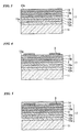
- FIG 1 is a view showing an example of a light-emitting diode that is an embodiment of the invention.
- the light-emitting diode (LED) 1 which is an embodiment of the invention, has a light-emitting portion 3 including a light-emitting layer 2, and a heatsink substrate 5 joined to the light-emitting portion 3 via a reflection structure 4.
- a first electrode 6 is provided on the surface 3a of the light-emitting portion 3 on the opposite side of the reflection structure 4
- a second electrode 8 is provided on the surface 3b of the light-emitting portion 3 on the reflection structure 4 side.
- the light-emitting portion 3 is a compound semiconductor-laminate structure including the light-emitting layer 2, which is an epitaxial laminate structure formed by laminating a plurality of epitaxially grown layers.
- the light-emitting portion 3 it is possible to use, for example, an AlGaInP layer, an AlGaAs layer, or the like having high light-emitting efficiency, for which a substrate joining technology is established.
- the AlGaInP layer is a layer made from a material represented by a general formula of (Al X Ga 1-X ) Y In 1-Y P (0 ⁇ X ⁇ 1, 0 ⁇ Y ⁇ 1). The composition is determined according to the light-emitting wavelength of the light-emitting diode.
- the composition of the constituent materials is determined according to the light-emitting wavelength of the light-emitting diode.
- the light-emitting portion 3 is a conductive compound semiconductor of either n-type or p-type and has a p-n junction formed therein. Additionally, the polarity on the surface of the light-emitting portion 3 may be any of p-type and n-type polarities.
- the light-emitting portion 3 is composed of, for example, a contact layer 12b, a cladding layer 10a, the light-emitting layer 2, a cladding layer 10b, and a GaP layer 13.
- the contact layer 12b is a layer for decreasing the contact resistance of an ohmic electrode, which is composed of, for example, Si-doped n-type (Al 0.5 Ga 0.5 ) 0.5 In 0.5 P, and is made to have a carrier concentration of 2 ⁇ 10 18 cm -3 and a thickness of 1.5 ⁇ m.
- the cladding layer 10a is composed of, for example, Si-doped n-type (Al 0.7 Ga 0.3 ) 0.5 In 0.5 P, and is made to have a carrier concentration of 8 ⁇ 10 17 cm -3 and a thickness of 1 ⁇ m.
- the light-emitting layer 2 is composed of, for example, 10 pairs of a laminate structure of undoped (Al 0.2 Ga 0.8 ) 0.5 In 0.5 P/(Al 0.7 Ga 0.3 ) 0.5 In 0.5 P), and is made to have a thickness of 0.8 ⁇ m.
- the light-emitting layer 2 has a structure of a double hetero (DH) structure, a single quantum well (SQW) structure, a multi quantum well (MQW) structure, or the like.
- the double hetero structure is a structure capable of confining carriers in charge of radiative recombination.
- the quantum well structure is a structure having a well layer and two well layers clipping the well layer, and the SQW has one well layer, and the MQW has two or more well layers.
- a method for forming the light-emitting portion 3 a MOCVD method or the like can be used.
- the MQW structure In order to produce light emission excellent in terms of monochromaticity from the light-emitting layer 2, in particular, it is preferable to use the MQW structure as the light-emitting layer 2.
- the cladding layer 10b is composed of, for example, Mg-doped p-type (Al 0.7 Ga 0.3 ) 0.5 In 0.5 P, and is made to have a carrier concentration of 2 ⁇ 10 17 cm -3 and a thickness of 1 ⁇ m.
- the GaP layer 13 is, for example, a Mg-doped p-type GaP layer, and is made to have a carrier concentration of 3 ⁇ 10 18 cm -3 and a thickness of 3 ⁇ m.
- the configuration of the light-emitting portion 3 is not limited to the above-described structures, and may have, for example, an electric current diffusion layer that diffuses electric current for driving elements in a planar manner throughout the light-emitting portion 3, or an electric current inhibition layer, an electric current narrowing layer, or the like for limiting areas where electric current for driving elements flows.
- Each of the first electrode 6 and the second electrode 8 is an ohmic electrode, and the shape and disposition thereof is not particularly limited as long as the electrode can uniformly diffuse electric current to the light-emitting portion 3.
- the shape and disposition thereof is not particularly limited as long as the electrode can uniformly diffuse electric current to the light-emitting portion 3.
- the first electrode 6 As a material for the first electrode 6, it is possible to use, for example, AuGe, AuSi, or the like when an n-type compound semiconductor is used as the contact layer 12b, and to use, for example, AuBe, AuZn, or the like when a p-type compound semiconductor is used as the contact layer 12b. In addition, it is possible to prevent oxidation and also to improve wire bonding by further laminating Au or the like thereon.
- the second electrode 8 As a material for the second electrode 8, it is possible to use, for example, AuGe, AuSi, or the like when an n-type compound semiconductor is used as the GaP layer 13, and to use, for example, AuBe, AuZn, or the like when a p-type compound semiconductor is used as the GaP layer 13.
- the reflection structure 4 is formed on the surface 3b of the light-emitting portion 3 on the reflection structure 4 side so as to cover the second electrode 8.
- the reflection structure 4 is formed by laminating a metallic film 15 and a transparent conductive film 14.
- the metallic film 15 is constituted by a metal, such as copper, silver, gold, aluminum, or the like, and an alloy thereof or the like.
- the materials have high light reflectivity and thus can achieve a light reflectivity of 90% or higher from the reflection structure 4.
- the metallic film 15 is made to have a laminate structure composed of an Ag alloy/W/Pt/Au/a connection metal from the transparent conductive film 14 side.
- the connection metal formed on the surface 15b of the metallic film 15 on the opposite side of the light-emitting portion 3 is a metal that has a low electrical resistance and is melted at a low temperature.
- the connection metal it is possible to connect a heatsink substrate without inducing thermal stress on the light-emitting portion 3.
- an Au-based eutectic metal or the like which is chemically stable and has a low melting point, is used.
- the Au-based eutectic metal can include a eutectic composition of an alloy, such as AuSn, AuGe, AuSi, or the like (Au-based eutectic metal).
- Au-based eutectic metal it is preferable to add a metal, such as titanium, chromium, tungsten, or the like, to the connection metal.
- the metal such as titanium, chromium, tungsten, or the like, can act as a barrier metal to prevent the impurities or the like included in the heatsink substrate from diffusing toward the metallic film 15 and causing some reactions.
- the transparent conductive film 14 is constituted by an ITO film, an IZO film, or the like. Meanwhile, the reflection structure 4 may be constituted by only the metallic film 15. In addition, instead of the transparent conductive film 14, or together with the transparent conductive film 14, a so-called cold mirror that uses the difference in the index of refraction between transparent materials may be combined with the metallic film 15, for example, using a multilayer film of a titanium oxide film and a silicon oxide film, white alumina, or AlN.
- a joining surface 5a of the heatsink substrate 5 is joined to the surface 15b of the metallic film 15 which constitutes the reflection structure 4 on the opposite side of the light-emitting portion 3.
- the thickness of the heatsink substrate 5 is preferably from 50 ⁇ m to 150 ⁇ m. When the thickness of the heatsink substrate 5 is larger than 150 ⁇ m, the costs for manufacturing a light-emitting diode are increased, which is not preferable. In addition, when the thickness of the heatsink substrate 5 is smaller than 50 ⁇ m, cracks, chips, warpage, or the like occur easily during handling so that there is concern regarding a decrease in the manufacturing yield ratio.
- the heatsink substrate 5 is formed by alternately laminating a first metal layer 21 and a second metal layer 22.
- the total number of the first metal layers 21 and the second metal layers 22 per heatsink substrate 1 is preferably from 3 layers to 9 layers, and more preferably from 3 layers to 5 layers.
- thermal expansion becomes uneven in the thickness direction so that there is concern regarding the occurrence of cracks in the heatsink substrate 5.
- the total number of the first metal layers 21 and the second metal layers 22 is set to more than 9 layers, it becomes necessary to reduce the thickness of each of the first metal layers 21 and the second metal layers 22.
- the total number of the first metal layers 21 and the second metal layers 22 is more preferably an odd number.
- the first metal layer 21 preferably has a thermal conductivity of 130 W/m ⁇ K or higher. Thereby, the thermal radiation properties of the heatsink substrate 5 are enhanced so that a light-emitting diode 1 is enabled to emit light with high luminance and also to have a longer service life.
- the first metal layer 21 is preferably made of a material having a thermal expansion coefficient substantially similar to the thermal expansion coefficient of the light-emitting portion 3.
- a material for the first metal layer 21 preferably has a thermal expansion coefficient within ⁇ 1.5 ppm/K of the thermal expansion coefficient of the light-emitting portion 3.
- the thermal conductivity of molybdenum is 138 W/m ⁇ K
- the thermal conductivity of tungsten is 174 W/m.K, and thus both materials have a thermal conductivity equal to or higher than 130 W/m ⁇ K.
- the total thickness of the first metal layers 21 is preferably from 10% to 45% of the thickness of the heatsink substrate 5, more preferably from 20% to 40%, and further preferably from 25% to 35%.
- the total thickness of the first metal layers 21 exceeds 45% of the thickness of the heatsink substrate 5, the effect of the second metal layer 22 having a high thermal conductivity is reduced so that the heatsink function is degraded.
- the thickness of the first metal layers 21 is less than 10% of the thickness of the heatsink substrate 5, the first metal layers 21 hardly function so that it is not possible to suppress heat-induced cracks in the heatsink substrate 5 when the heatsink substrate 5 and the light-emitting portion 3 are brought into contact.
- the total thickness of molybdenum is preferably from 15% to 45% of the thickness of the heatsink substrate 5, more preferably from 20% to 40%, and further preferably from 25% to 35%.
- the thickness of the first metal layer 21 is preferably from 10 ⁇ m to 40 um, and more preferably from 20 ⁇ m to 30 ⁇ m.
- the second metal layer 22 is preferably made of a material having a thermal conductivity higher than at least that of the first metal layer 21, and more preferably a material having a thermal conductivity of 230 W/m.K or higher. Thereby, the thermal radiation properties of the heatsink substrate 5 are enhanced so that a light-emitting diode 1 is enabled to emit light with high luminance and also to have a longer service life.
- the thickness of the second metal layer 22 is preferably from 10 ⁇ m to 40 ⁇ m, and more preferably from 20 ⁇ m to 40 ⁇ m. Meanwhile, the thicknesses of the first metal layer 21 and the second metal layer 22 may be different. Furthermore, when the heatsink substrate 5 is formed with a plurality of the first metal layers 21 and the second metal layers 22, the thickness of each layer may be different.
- a joining auxiliary film that stabilizes electrical contact or a eutectic metal for die bonding may be formed on the joining surface 5a of the heatsink substrate 5. Thereby, a joining process can be easily performed.
- As the joining auxiliary film Au, AuSn, or the like can be used.
- the method for joining the heatsink substrate 5 to the light-emitting portion 3 is not limited to the above-described method, and it is possible to apply a well-known technology, for example, diffused junction, an adhesive, a room temperature joining method, or the like.
- the light-emitting diode 1 which is an embodiment of the invention, is a light-emitting diode 1 having the heatsink substrate 5 joined to the light-emitting portion 3 including the light-emitting layer 2, in which the heatsink substrate 5 is formed by alternately laminating the first metal layer 21 and the second metal layer 22;
- the first metal layer 21 has a thermal conductivity of 130 W/m.K or higher and is made of a material having a thermal expansion coefficient substantially similar to the thermal expansion coefficient of a material for the light-emitting portion 3;
- the second metal layer 22 is made of a material having a thermal conductivity of 230 W/m ⁇ K or higher.
- the light-emitting diode 1 of the invention may have excellent thermal radiation properties and is capable of suppressing cracks in a substrate during joining and of emitting light with high luminance by applying a high voltage to the diode 1.
- the light-emitting diode 1 which is an embodiment of the invention, has the first metal layers 21 made of a material having a thermal expansion coefficient within ⁇ 1.5 ppm/K of the thermal expansion coefficient of the light-emitting portion 3.
- the light-emitting diode 1 of the invention may have excellent thermal radiation properties and is capable of suppressing cracks in a substrate during joining and of emitting light with high luminance by applying a high voltage to the diode 1.
- the light-emitting diode 1 which is an embodiment of the invention, has the first metal layers 21 made of molybdenum, tungsten, or an alloy thereof.
- the light-emitting diode 1 of the invention may have excellent thermal radiation properties and is capable of suppressing cracks in a substrate during joining and of emitting light with high luminance by applying a high voltage to the diode 1.
- the light-emitting diode 1 which is an embodiment of the invention, has the second metal layer 22 made of aluminum, copper, silver, gold, an alloy thereof, or the like.
- the light-emitting diode 1 of the invention may have excellent thermal radiation properties and is capable of suppressing cracks in a substrate during joining and of emitting light with high luminance by applying a high voltage to the diode 1.
- the light-emitting diode 1 which is an embodiment of the invention, has the first metal layers 21 made of molybdenum and the second metal layer 22 made of copper, in which the total number of the first metal layers 21 and the second metal layer 22 is from 3 layers to 9 layers.
- the light-emitting diode 1 of the invention may have excellent thermal radiation properties and is capable of suppressing cracks in a substrate during joining and of emitting light with high luminance by applying a high voltage to the diode 1.
- the second metal layer 22 may be disposed at the position of the first metal layer 21, and the first metal layer 21 may be disposed at the position of the second metal layer 22. In the case of the above embodiment, the same effect can be obtained even when a copper layer is disposed at the position of the first metal layer 21 and a molybdenum layer is disposed at the position of the second metal layer 22.
- a method for manufacturing the light-emitting diode includes a process for manufacturing the heatsink substrate; a process in which a light-emitting portion including the light-emitting layer is formed on a semiconductor substrate via a buffer layer, and then the second electrode is formed on the surface of the light-emitting portion on the opposite side of the semiconductor substrate; a process in which a reflection structure is formed on the surface of the light-emitting portion on the opposite side of the semiconductor substrate via the second electrode; a process in which a heatsink substrate is joined to the light-emitting portion via the reflection structure; a process in which the semiconductor substrate and the buffer layer are removed; and a process in which a first electrode is formed on the surface of the light-emitting portion on the opposite side of the heatsink substrate.
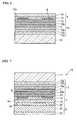
- the process for manufacturing the heatsink substrate will be described.
- the heatsink substrate 5 has a thermal conductivity of 130 W/m ⁇ K or higher, and is formed by hot-pressing the first metal layers having a thermal expansion coefficient substantially similar to the thermal expansion coefficient of the light-emitting portion and the second metal layer having a thermal conductivity of 230 W/m ⁇ K or higher.
- first metal plates 21 and a substantially plain plate-shaped second metal plate 22 are prepared.
- Mo with a thickness of 25 ⁇ m is used as the first metal plate 21
- Cu with a thickness of 70 ⁇ m is used as the second metal plate 22.
- the second metal plate 22 is inserted between two first metal plates 21 so as to be disposed between the first metal plates 21.
- the substrate is disposed in a predetermined pressing apparatus, and load is applied to the first metal plate 21 and the second metal plate 22 in the arrow direction under a high temperature.
- the heatsink substrate 5 composed of 3 layers of Mo (25 ⁇ m)/Cu (70 ⁇ m)/Mo (25 ⁇ m) is formed, in which the first metal plate 21 is Mo and the second metal plate 22 is Cu.
- the heatsink substrate 5 has, for example, a thermal expansion coefficient of 5.7 ppm/K and a thermal conductivity of 220 W/m.K.
- the substrate may be cut according to the size of the joining surface of the light-emitting portion (wafer) 3 and then be mirror-finished for the surfaces.
- a joining auxiliary film may be formed on the joining surface 5a of the heatsink substrate 5 in order to stabilize electrical contact.
- gold, platinum, nickel, or the like can be used as the joining auxiliary film.
- a eutectic metal such as AuSn or the like, for die bonding may be formed. Thereby, a joining process can be easily performed.
- a plurality of epitaxial layers is grown on a surface 11a of the semiconductor substrate 11 so as to form an epitaxial laminate 17.
- the semiconductor substrate 11 is a substrate for forming the epitaxial laminate 17, which is, for example, a Si-doped n-type GaAs single crystal substrate having the surface 11a inclined at 15 degrees from the (100) plane.
- a gallium arsenide (GaAs) single crystal substrate As such, when an AlGaInP layer or an AlGaAs layer is used as the epitaxial laminate 17, it is possible to use a gallium arsenide (GaAs) single crystal substrate as the substrate for forming the epitaxial laminate 17.
- MOCVD metal organic chemical vapor deposition
- MBE molecular beam epitaxy
- LPE liquid phase epitaxy
- each of the layers is epitaxially grown using a reduced-pressure MOCVD method in which trimethylaluminum ((CH 3 ) 3 Al), trimethylgallium ((CH 3 ) 3 Ga), and trimethylindium ((CH 3 ) 3 In) are used as the raw materials of constituent elements belonging to Group III.
- biscyclopentadienyl magnesium bis-(C 5 H 5 ) 2 Mg
- disilane Si 2 H 6
- phosphine (PH 3 ) or arsine (AsH 3 ) is used as the raw material of constituent elements belonging to Group V.
- the p-type GaP layer 13 is grown at, for example, 750 °C, and the other epitaxially grown layers are grown at, for example, 730 °C.
- the buffer layer 12a composed of Si-doped n-type GaAs is formed on the surface 11a of the semiconductor substrate 11.
- the buffer layer 12a for example, Si-doped n-type GaAs is used, which has a carrier concentration of 2 ⁇ 10 18 cm -3 and a thickness of 0.2 ⁇ m.
- the contact layer 12b composed of Si-doped n-type (Al 0.5 Ga 0.5 ) 0.5 In 0.5 P is formed on the buffer layer 12a.
- the cladding layer 10a composed of Si-doped n-type (Al 0.7 Ga 0.3 ) 0.5 In 0.5 P is formed.
- the light-emitting layer 2 composed of 10 pairs of laminate structures of undoped (Al 0.2 Ga 0.8 ) 0.5 In 0.5 P/(Al 0.7 Ga 0.3 ) 0.5 In 0.5 P) is formed.
- the cladding layer 10b composed of Mg-doped p-type (Al 0.7 Ga 0.3 ) 0.5 In 0.5 P is formed.
- the Mg-doped p-type GaP layer 13 is formed on the cladding layer 10b.
- the second electrode (ohmic electrode) 8 is formed on the surface 13a of the p-type GaP layer 13 on the opposite side of the semiconductor substrate 11.
- the second electrode 8 is formed by, for example, laminating 0.2 ⁇ m-thick Au on 0.4 ⁇ m-thick AuBe.
- the second electrode 8 is shaped like a circle with a diameter of 20 ⁇ m, when viewed from the top, and is formed at an interval of 60 ⁇ m.
- the transparent conductive film 14 composed of an ITO film is formed so as to cover the surface 13a of the p-type GaP layer 13 on the opposite side of the semiconductor substrate 11 and the second electrode 8.
- a thermal treatment is performed at 450 °C so as to form ohmic contact between the second electrode 8 and the transparent conductive film 14.
- a 0.5 ⁇ m-thick film composed of a silver (Ag) alloy is formed on the surface 14a of the transparent conductive film 14 on the opposite side of the epitaxial laminate 17 using a vapor deposition method
- a 0.1 ⁇ m-thick tungsten (W) film, a 0.1 ⁇ m-thick platinum (Pt) film, a 0.5 ⁇ m-thick gold (Au) film, and 1 ⁇ m-thick AuGe eutectic metal (with a melting point of 386 °C) are formed so as to produce the metal film 15.
- the reflection structure 4 constituted by the metallic film 15 and the transparent conductive film 14 is formed.
- the semiconductor substrate 11, on which the reflection structure 4 and the epitaxial laminate 17 are formed, and the heatsink substrate 5 formed in the process for manufacturing the heatsink substrate are transported in a decompression apparatus and are disposed in a manner such that the joining surface 4a of the reflection structure 4 and the joining surface 5a of the heatsink substrate 5 face each other.
- the joining surface 4a of the reflection structure 4 and the joining surface 5a of the heatsink substrate 5 are joined by applying a load of 100 g/cm 2 in a state in which the semiconductor substrate 11 and the heatsink substrate 5 are heated to 400 °C, thereby forming a joined structure 18.
- the semiconductor substrate 11 and the buffer layer 12a are selectively removed from the joined structure 18 using an ammonia-based etchant. Thereby, the light-emitting portion 3 having the light-emitting layer 2 is formed.
- a conductive film for electrodes is formed on the surface 3a of the light-emitting portion 3 on the opposite side of the reflection structure 4 using a vacuum deposition method.
- a metal layer structure composed of AuGe/Ni /Au can be used as the conductive film for electrodes.
- AuGe with 12% of Ge mass ratio
- a 0.05 ⁇ m-thick layer ofNi is formed, and, furthermore, a 1 ⁇ m-thick layer of Au is formed.
- the conductive film for the electrode is patterned into a circle shape when viewed from the top, which acts as an n-type ohmic electrode (first electrode) 6, thereby manufacturing the light-emitting diode 1 shown in FIG 1 .
- each metal of the n-type ohmic electrode (first electrode) 6 is alloyed by, for example, performing a thermal treatment at 420 °C for 3 minutes. Thereby, it is possible to reduce the resistance of the n-type ohmic electrode (first electrode) 6.
- the substrate at the cutting parts and a connection layer are cut into a desired size of light-emitting diode chips (LED chips) using a laser with a 0.8-mm pitch.
- the size of the light-emitting diode refers to, for example, the diagonal length of the substantially rectangular light-emitting portion 3 when viewed from the top, which is set to 1.1 mm.
- the heatsink substrate is joined to the light-emitting diode, high light-emitting efficiency can be obtained even in a high electric current zone.
- the method for manufacturing the light-emitting diode includes a process in which the light-emitting portion 3 including the light-emitting layer 2 is formed on the semiconductor substrate 11 via the buffer layer 12a, and then the second electrode 8 is formed on the surface 13a of the light-emitting portion 3 on the opposite side of the semiconductor substrate 11; a process in which the reflection structure 4 is formed on the surface 13a of the light-emitting portion 3 on the opposite side of the semiconductor substrate 11 via the second electrode 8; a process in which the heatsink substrate 5 is joined to the light-emitting portion 3 via the reflection structure 4; a process in which the semiconductor substrate 11 and the buffer layer 12a are removed; and a process in which the first electrode 6 is formed on the surface 3a of the light-emitting portion 3 on the opposite side of the heatsink substrate 5.
- the method for manufacturing the light-emitting diode of the invention is possible to manufacture a light-emitting diode that is excellent in terms of thermal radiation properties and is capable of emitting light with high luminance by suppressing cracks in the substrate during joining and by applying a high voltage to the diode.
- the heatsink substrate 5 is formed by pressing the first metal layers 21, which has a thermal conductivity of 130 W/m ⁇ K or higher and a thermal expansion coefficient substantially similar to the thermal expansion coefficient of the light-emitting portion, and the second metal layer 22 having a thermal conductivity of 230 W/m ⁇ K or higher at a high temperature.
- the method for manufacturing the light-emitting diode of the invention is possible to manufacture a light-emitting diode that is excellent in terms of thermal radiation properties and is capable of emitting light with high luminance by suppressing cracks in the substrate during joining and by applying a high voltage to the diode.
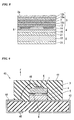
- FIG 9 is a schematic cross-sectional view showing an example of a light-emitting diode lamp, which is an embodiment of the invention.
- a light-emitting diode lamp 40 which is an embodiment of the invention, includes a package substrate 45, two electrode terminals 43 and 44 formed on the package substrate 45, a light-emitting diode 1 mounted on the electrode terminal 44, and a transparent resin (sealing resin) 41 composed of silicon or the like, which is formed to cover the light-emitting diode 1.
- the light-emitting diode 1 has the light-emitting portion 3, the reflection structure 4, the heatsink substrate 5, the first electrode 6, and the second electrode 8, in which the heatsink substrate 5 is disposed to be connected to the electrode terminal 43.
- the first electrode 6 and the electrode terminal 44 are wire-bonded. Voltage applied to the electrode terminals 43 and 44 is applied to the light-emitting portion 3 via the first electrode 6 and the second electrode 8 so that the light-emitting layer included in the light-emitting portion 3 emits light. Emitted light is extracted in the front direction f.
- the package substrate 45 is made to have a thermal resistance of 10 °C/W or lower. Thereby, even when 1 W or higher of electric power is applied to the light-emitting layer 2 so as to emit light, it is possible to make the package substrate act as a heatsink and to further increase the thermal radiation properties of the light-emitting diode 1. Meanwhile, the shape of the package substrate is not limited thereto, and a package substrate having another shape may be used. Since thermal radiation properties can be sufficiently secured even in an LED lamp product using a package substrate having another shape, it is possible to produce a high-power and high luminance light-emitting diode lamp.
- the light-emitting diode package 40 which is an embodiment of the invention, is the light-emitting diode lamp 40 having the light-emitting diode 1 and the package substrate 45 mounting the light-emitting diode 1, and the thermal resistance of the package substrate 45 is 10 °C/W or lower.
- the light-emitting diode package 40 of the invention may have excellent thermal radiation properties and emit light with high luminance by applying a high voltage to the diode.
- the light-emitting diode package 40 which is an embodiment of the invention, emits light by adding 1 W or higher of electric power to the light-emitting layer 2 in the light-emitting diode 1, it is possible to be excellent in terms of thermal radiation properties and to emit light with high luminance by applying a high voltage.
- FIG 10 is a view showing a second example of the light-emitting diode, which is an embodiment of the invention.
- a light-emitting diode (LED) 51 which is an embodiment of the invention, is configured in the same manner as the first embodiment except that a heatsink substrate 55 is used instead of the heatsink substrate 5.
- members the same as those shown in the first embodiment are given the same reference signs.
- the light-emitting diode (LED) 51 which is an embodiment of the invention, has the light-emitting portion 3 including the light-emitting layer (not shown), and the heatsink substrate 55 joined to the light-emitting portion 3 via the reflection structure 4.
- the first electrode 6 is provided on the surface 3a of the light-emitting portion 3 on the opposite side of the reflection structure 4
- the second electrode 8 is provided on the surface 3b of the light-emitting portion 3 on the reflection structure 4 side.
- a 5-layer structure substrate (with a thickness of 127 ⁇ m) of Mo (1 ⁇ m)/Cu (50 ⁇ m)/Mo (25 ⁇ m)/Cu (50 ⁇ m)/Mo (1 ⁇ m) is used as the heatsink substrate 55, in which Mo is used as the first metal layer 21 and Cu is used as the second metal layer 22.
- a method for manufacturing the heatsink substrate 55 will be described. Using the method for manufacturing the heatsink substrate shown in the first embodiment, firstly, a 3-layer structure substrate of Cu (50 ⁇ m)/Mo (25 ⁇ m)/Cu (50 ⁇ m) is manufactured, and then 1 ⁇ m-thick Mo is formed on both surfaces of the 3-layer structure substrate using a sputtering method so that the heatsink substrate 55 composed of a 5-layer structure is formed. Meanwhile, the heatsink substrate 55 has a thermal expansion coefficient of 6.6 ppm/K and a thermal conductivity of 230 W/m.K.
- FIG 11 is a view showing a third example of the light-emitting diode, which is an embodiment of the invention.
- a light-emitting diode (LED) 52 which is an embodiment of the invention, is configured in the same manner as the first embodiment except that a heatsink substrate 56 is used instead of the heatsink substrate 5.
- members the same as those shown in the first embodiment are given the same reference signs.
- the light-emitting diode (LED) 52 which is an embodiment of the invention, has the light-emitting portion 3 including the light-emitting layer (not shown), and the heatsink substrate 56 joined to the light-emitting portion 3 via the reflection structure 4.
- the first electrode 6 is provided on the surface 3a of the light-emitting portion 3 on the opposite side of the reflection structure 4
- the second electrode 8 is provided on the surface 3b of the light-emitting portion 3 on the reflection structure 4 side.
- a 3-layer structure substrate (with a thickness of 85 ⁇ m) of Cu (30 ⁇ m)/Mo (25 ⁇ m)/Cu (30 ⁇ m) is used as the heatsink substrate 56, in which Mo is used as the first metal layer 21 and Cu is used as the second metal layer 22.
- a method for manufacturing the heatsink substrate 56 will be described. Using the method for manufacturing the heatsink substrate shown in the first embodiment, the heatsink substrate 56 composed of a 3-layer structure substrate of Cu (30 ⁇ m)/Mo (25 ⁇ m)/Cu (30 ⁇ m) is manufactured. Meanwhile, the heatsink substrate 56 has a thermal expansion coefficient of 6.1 ppm/K and a thermal conductivity of 250 W/m ⁇ K.
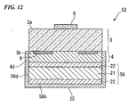
- FIG 12 is a view showing a fourth example of the light-emitting diode, which is an embodiment of the invention.
- a light-emitting diode (LED) 53 which is an embodiment of the invention, is configured in the same manner as the third embodiment except that a metal laminate film 25 is formed so as to cover the side surface 4d of the reflection structure 4, and the side surface 56d and the bottom surface 56e of a heatsink substrate 56.
- members the same as those shown in the first embodiment are given the same reference signs.
- the light-emitting diode (LED) 53 which is an embodiment of the invention, has the light-emitting portion 3 including the light-emitting layer (not shown), and the heatsink substrate 56 joined to the light-emitting portion 3 via the reflection structure 4.
- the first electrode 6 is provided on the surface 3a of the light-emitting portion 3 on the opposite side of the reflection structure 4
- the second electrode 8 is provided on the surface 3b of the light-emitting portion 3 on the reflection structure 4 side.
- the surface (bottom surface) 56b of the heatsink substrate 56 on the opposite side of the light-emitting portion 3 is made of copper, and the metal laminate film 25 composed of a Ni layer and an Au layer is formed so as to cover the bottom surface 56b and the side surface 56d of the heatsink substrate 56 and the side surface 4d of the reflection structure 4.
- the metal laminate film 25 By forming the metal laminate film 25, it is possible to enhance the thermal radiation properties. Meanwhile, a plating method or the like can be used as a method for forming the Ni layer and the Au layer.
- a heatsink substrate of Example 1 composed of a 3-layer structure of Mo (25 ⁇ m)/Cu (70 ⁇ m)/Mo (25 ⁇ m) was formed. Meanwhile, a Pt (0.1 ⁇ m)/Au (0.5 ⁇ m) film was formed on the joining surface of the heatsink substrate.
- the heatsink substrate of Example 1 had a thermal expansion coefficient of 5.7 ppm/K and a thermal conductivity of 220 W/m.K.
- the contact layer 12b was composed of Si-doped n-type (Al 0.5 Ga 0.5 ) 0.5 In 0.5 P, and was made to have a carrier concentration of 2 ⁇ 10 18 cm -3 and a thickness of 1.5 ⁇ m.
- the cladding layer 10a was composed of S i-doped n-type (Al 0.7 Ga 0.3 ) 0.5 In 0.5 P, and was made to have a carrier concentration of 8 ⁇ 10 17 cm -3 and a thickness of 1 ⁇ m.
- the light-emitting layer 2 was composed of 10 pairs of laminate structures of undoped (Al 0.2 Ga 0.8 ) 0.5 In 0.5 P/(Al 0.7 Ga 0.3 ) 0.5 In 0.5 P), and was made to have a thickness of 0.8 ⁇ m.
- the cladding layer 10b was composed of Mg-doped p-type (Al 0.7 Ga 0.3 ) 0.5 In 0.5 P, and was made to have a carrier concentration of 2 ⁇ 10 17 cm -3 and a thickness of 1 ⁇ m.
- the GaP layer 13 was a Mg-doped p-type GaP layer, and was made to have a carrier concentration of 3 ⁇ 10 18 cm -3 and a thickness of 3 ⁇ m.
- a first electrode was formed to have a laminate structure of AuGe/Ni/Au
- a second electrode was formed to have a laminate structure of AuBe/Au
- a reflection structure was made to have a laminate structure composed of a transparent conductive film, which is composed of ITO, and a Ag alloy/W/Pt/Au/AuGe. Red light with the main wavelength of 620 nm was emitted by applying 2.4 V to the light-emitting diode of Example 1 and by flowing 500 mA of electric current. High light-emitting efficiency of about 651 m/W was obtained. At this time, due to the effects of the heatsink substrate, the light-emitting diode did not exhibit a decrease in the efficiency induced by an increase in temperature.
- a heatsink substrate of Example 2 composed of a 5-layer structure (with a thickness of 127 ⁇ m) of Mo (1 ⁇ m)/Cu (50 ⁇ m)/Mo (25 ⁇ m)/Cu (50 ⁇ m)/Mo (1 ⁇ m) was manufactured.
- the heatsink substrate of Example 2 had a thermal expansion coefficient of 6.6 ppm/K and a thermal conductivity of 230 W/m ⁇ K.
- Example 2 a light-emitting diode of Example 2 was manufactured in the same manner as Example 1 except that the heatsink substrate of Example 2 was used. Red light with the main wavelength of 620 nm was emitted by applying 2.4 V to the light-emitting diode of Example 2 and by flowing 500 mA of electric current. A high light-emitting efficiency of about 691 m/W was obtained. At this time, due to the effects of the heatsink substrate, the light-emitting diode did not exhibit a decrease in the efficiency induced by an increase in temperature.
- a heatsink substrate of Example 3 composed of a 3-layer structure (with a thickness of 85 ⁇ m) of Cu (30 ⁇ m)/Mo (25 ⁇ m)/Cu (30 ⁇ m) was manufactured.
- the heatsink substrate of Example 3 had a thermal expansion coefficient of 6.1 ppm/K and a thermal conductivity of 250 W/m.K.
- Example 3 a light-emitting diode of Example 3 was manufactured in the same manner as Example 1 except that the heatsink substrate of Example 3 was used. Red light with a main wavelength of 620 nm was emitted by applying 2.4 V to the light-emitting diode of Example 3 and by flowing 500 mA of electric current. A high light-emitting efficiency of about 711 m/W was obtained. At this time, due to the effects of the heatsink substrate, the light-emitting diode did not exhibit a decrease in the efficiency induced by an increase in temperature.
- a light-emitting diode of Comparative Example 1 was manufactured in the same manner as Example 1 except that a Si substrate was used as the heatsink substrate. Meanwhile, the Si substrate had a thermal expansion coefficient of 3 ppm/K and a thermal conductivity of 126 W/m.K. Red light with a main wavelength of 620 nm was emitted by applying 2.4 V to the light-emitting diode of Comparative Example 1 and by flowing 500 mA of electric current. At this time, the light-emitting efficiency of the light-emitting diode of Comparative Example 1 was decreased due to an increase in temperature so as to exhibit about 491 m/W. In addition, 4 of the 10 fed wafers were cracked during the production process. In summary, the cracking ratio (cracking ratio of the wafer) was 40%, which showed a problem in terms of productivity.
- a light-emitting diode of Comparative Example 2 was manufactured in the same manner as Example 1 except that a Cu substrate was used as the heatsink substrate. Similarly to Example 1, cracks occurred throughout a wafer when a light-emitting portion and a reflection structure were formed, and then the heatsink substrate was joined thereto. The Cu substrate was considered to have been cracked because the thermal expansion coefficient of the Cu substrate was large.
- Light-emitting diodes having the heatsink substrates shown in Table 1 were manufactured in the same manner as Examples 1 to 3 and Comparative Examples 1 and 2. With regard to the light-emitting diodes of Examples 1 to 3 and Comparative Examples 1 to 5, cracks in the wafers and the light-emitting efficiencies (when the electric current value was 500 mA) were investigated and shown in Table 1. As shown in Table 1, no cracks occurred in the light-emitting diodes of Comparative Examples 3 to 5, but the thermal conductivity of the heatsink substrates of the light-emitting diodes of Comparative Examples 3 to 5 were small, and the light-emitting efficiencies of the light-emitting diodes of Comparative Examples 3 to 5 were decreased due to an increase in temperature.
- the light-emitting diode of the invention can be improved in terms of thermal radiation properties and thus can be used for a variety of display lamps, lighting devices, or the like that emit light with unprecedentedly high luminance, and has applicability in industries manufacturing and using the display lamps, lighting devices, or the like.
Landscapes
- Led Device Packages (AREA)
- Led Devices (AREA)
- Non-Portable Lighting Devices Or Systems Thereof (AREA)
Abstract
The object of the invention is to provide a light-emitting diode that is excellent in terms of thermal radiation properties and is capable of suppressing cracks in the substrate during joining and emitting light with high luminance by applying a high voltage, a light-emitting diode lamp, and a method of manufacturing a light-emitting diode. The above object is achieved by using a light-emitting diode (1) having a heatsink substrate (5) joined to a light-emitting portion (3) including a light-emitting layer (2), in which the heatsink substrate (5) is formed by alternately laminating a first metal layer (21) and a second metal layer (22); the first metal layer (21) has a thermal conductivity of 130 W/m·K or higher and is made of a material having a thermal expansion coefficient substantially similar to the thermal expansion coefficient of a material for the light-emitting portion (3); and the second metal layer (22) is made of a material having a thermal conductivity of 230 W/m.K or higher.
Description
- The present invention relates to a light-emitting diode, a light-emitting diode lamp, and a method for manufacturing a light-emitting diode.
- As a light-emitting diode (English abbreviation: LED) that emits visible light, such as red, orange, yellow, yellow-green, or the like, a compound semiconductor LED is known which includes a light-emitting portion having a light-emitting layer composed of, for example, aluminum phosphide, gallium, and indium (with an compositional formula of (AlXGa1-X)YIn1-YP; 0≤X≤1, 0<Y≤1) and a substrate on which the light-emitting portion is formed.
- As the substrate, gallium arsenide (GaAs) or the like, which is optically opaque with respect to light emitted from the light-emitting layer and is also not very strong mechanically, is generally used.
However, in recent years, in order to produce a visible light-emitting diode with higher luminance, for the purpose of further improvement in the mechanical strength of a light-emitting element, the substrate is removed, and then a supporter layer (substrate) composed of a material that transmits or reflects emitted light and is excellent in terms of mechanical strength is joined thereto.
For example, PLTs 1 to 7 discloses technologies in which the supporter layer (substrate) is further joined to the light-emitting layer (joined LED-forming technologies). Furthermore, PLT 8 discloses a technology related to the above joining technology which is a light-emitting element having an ohmic metal implanted in an organic adhesion layer between a metal layer and a reflection layer. - As a result of the development of the joined LED-forming technologies, the degree of freedom of a substrate joined to a light-emitting portion has increased, and the use of a heatsink substrate composed of, for example, a metal with high thermal radiation properties, a ceramic, or the like has become possible. The use of a heatsink substrate as the substrate secures thermal radiation properties from the light-emitting portion so as to make it possible to suppress degradation of a light-emitting layer and to increase the service life.
Particularly, with regard to a high output light-emitting diode that needs to tolerate high electric current so as to shine with high luminance, the securement of thermal radiation properties becomes a more important issue due to the larger heating value than that in the related art. Therefore, joining a heatsink substrate to a light-emitting portion is more useful to prolong the service life of a light-emitting diode. - However, since the heatsink substrate composed of a metal with high thermal radiation properties, a ceramic, or the like has a thermal expansion coefficient that is significantly different from the thermal expansion coefficient of the light-emitting portion, there have been cases in which cracks occurred in the light-emitting portion and/or the heatsink substrate when the heatsink substrate was joined to the light-emitting portion or in the subsequent thermal treatments or the like. As a result, there have been cases in which the yield ratio of the manufacture of a light-emitting diode has been significantly lowered.
- As a heatsink substrate, if it is possible to use a material having a thermal expansion coefficient within 1 ppm/K of the thermal expansion coefficient of the light-emitting portion and a thermal conductivity of 200 W/K or higher, it is possible to suppress an occurrence of cracks or the like in the thermal treatments or the like and to sufficiently secure thermal radiation properties. However, no materials have been reported that can satisfy both characteristics of the thermal expansion coefficient and the thermal conductivity.
-
- [Patent Literature 1]
Japanese Patent No.3230638 - [Patent Literature 2]
Japanese Unexamined Patent Application, First Publication No.6-302857 - [Patent Literature 3]
Japanese Unexamined Patent Application, First Publication No.2002-246640 - [Patent Literature 4]
Japanese Patent No.2588849 - [Patent Literature 5]
Japanese Unexamined Patent Application, First Publication No.2001-57441 - [Patent Literature 6]
Japanese Unexamined Patent Application, First Publication No.2007-81010 - [Patent Literature 7]
Japanese Unexamined Patent Application, First Publication No.2006-32952 - [Patent Literature 8]
Japanese Unexamined Patent Application, First Publication No.2005-236303 - The invention has been made in consideration of the above circumstances, and the object of the invention is to provide a light-emitting diode that is excellent in terms of thermal radiation properties and is capable of suppressing cracks in the substrate during joining and emitting light with high luminance by applying a high voltage, a light-emitting diode lamp, and a method of manufacturing a light-emitting diode.
- In order to achieve the above object, the invention adopts the following configurations. That is,
- (1) A light-emitting diode of the invention is a light-emitting diode having a heatsink substrate joined to a light-emitting portion including a light-emitting layer, in which the heatsink substrate is formed by alternately laminating a first metal layer and a second metal layer; the first metal layer has a thermal conductivity of 130 W/m·K or higher and is made of a material having a thermal expansion coefficient substantially similar to the thermal expansion coefficient of a material for the light-emitting portion; and the second metal layer is made of a material having a thermal conductivity of 230 W/m·K or higher.
-
- (2) In the light-emitting diode of the invention, a material for the first metal layer is a material having a thermal expansion coefficient within ±1.5 ppm/K of the thermal expansion coefficient of the light-emitting portion.
- (3) In the light-emitting diode of the invention, the first metal layer is made of molybdenum, tungsten, or an alloy thereof.
- (4) In the light-emitting diode of the invention, the second metal layer is made of aluminum, copper, silver, gold, an alloy thereof, or the like.
-
- (5) In the light-emitting diode of the invention, the first metal layer is made of molybdenum; the second metal layer is made of copper; and the total number of the first metal layers and the second metal layers is from 3 layers to 9 layers.
- (6) In the light-emitting diode of the invention, the first metal layer is made of molybdenum, and the total thickness of the first metal layers is from 15% to 45% of the thickness of the heatsink substrate.
- (7) The light-emitting diode of the invention includes a reflection structure between the light-emitting portion and the heatsink substrate.
-
- (8) In the light-emitting diode of the invention, the light-emitting layer includes an AlGaInP layer or an AlGaAs layer.
- (9) In the light-emitting diode of the invention, the light-emitting layer has a substantially rectangular shape with a diagonal length of 1 mm or larger when viewed from the top, and light is emitted by applying 1 W or more of electric power to the light-emitting layer.
- (10) In the light-emitting diode of the invention, the surface of the heatsink substrate on the opposite side of the light-emitting portion is made of copper, and a metal laminate film is formed so as to cover the surface on the opposite side of the light-emitting portion and a side surface of the heatsink substrate.
-
- (11) A light-emitting diode lamp of the invention is a light-emitting diode lamp having the above-described light-emitting diode and a package substrate mounting the light-emitting diode, in which the thermal resistance of the package substrate is 10 °C/W or lower.
- (12) In the light-emitting diode lamp of the invention, light is emitted by applying 1 W or more of electric power to a light-emitting layer of the light-emitting diode.
- (13) A method for manufacturing a light-emitting diode of the invention includes a process in which a light-emitting portion including a light-emitting layer is formed on a semiconductor substrate via a buffer layer, and then a second electrode is formed on the surface of the light-emitting portion on the opposite side of the semiconductor substrate;
a process in which a reflection structure is formed on the surface of the light-emitting portion on the opposite side of the semiconductor substrate via the second electrode; a process in which a heatsink substrate is joined to the light-emitting portion via the reflection structure; a process in which the semiconductor substrate and the buffer layer are removed; and a process in which a first electrode is formed on the surface of the light-emitting portion on the opposite side of the heatsink substrate. - (14) In the method for manufacturing a light-emitting diode of the invention, the heatsink substrate is formed by pressing first metal layers, which has a thermal conductivity of 130 W/m·K or higher and a thermal expansion coefficient substantially similar to the thermal expansion coefficient of the light-emitting portion, and a second metal layer having a thermal conductivity of 230 W/m·K or higher at a high temperature.
- According to the above configuration, it is possible to provide a light-emitting diode that is excellent in terms of thermal radiation properties and is capable of suppressing cracks in a substrate during joining and of emitting light with high luminance by applying a high voltage, a light-emitting diode lamp, and a method for manufacturing a light-emitting diode.
- The light-emitting diode of the invention is a light-emitting diode having a heatsink substrate joined to a light-emitting portion including a light-emitting layer, in which the heatsink substrate is formed by alternately laminating a first metal layer and a second metal layer; the first metal layer has a thermal conductivity of 130 W/m·K or higher and is made of a material having a thermal expansion coefficient substantially similar to the thermal expansion coefficient of a material for the light-emitting portion; and the second metal layer is made of a material having a thermal conductivity of 230 W/m.K or higher. Thus, the light-emitting diode of the invention may have excellent thermal radiation properties and is capable of suppressing cracks in a substrate during joining and of emitting light with high luminance by applying a high voltage to the diode.
- The light-emitting diode lamp of the invention is a light-emitting diode lamp having the above-described light-emitting diode and a package substrate mounting the light-emitting diode, and the thermal resistance of the package substrate is 10 °C/W or lower. Thus, the light-emitting diode lamp of the invention may have excellent thermal radiation properties and is capable of emitting light with high luminance by applying a high voltage to the diode lamp.
- The method for manufacturing the light-emitting diode of the invention includes a process in which the light-emitting portion including the light-emitting layer is formed on the semiconductor substrate via the buffer layer, and then the second electrode is formed on the surface of the light-emitting portion on the opposite side of the semiconductor substrate; a process in which the reflection structure is formed on the surface of the light-emitting portion on the opposite side of the semiconductor substrate via the second electrode; a process in which the heatsink substrate is joined to the light-emitting portion via the reflection structure; a process in which the semiconductor substrate and the buffer layer are removed; and a process in which the first electrode is formed on the surface of the light-emitting portion on the opposite side of the heatsink substrate. Thus, the method for manufacturing the light-emitting diode of the invention is possible to manufacture a light-emitting diode that is excellent in terms of thermal radiation properties and is capable of suppressing cracks in the substrate during joining and of emitting light with high luminance by applying a high voltage to the diode.
-
-
Fig. 1 is a cross-sectional view showing an example of a light-emitting diode that is an embodiment of the invention. -
Fig. 2 is a cross-sectional view of a process showing an example of a manufacturing process of a heatsink substrate used for a light-emitting diode that is an embodiment of the invention. -
Fig. 3 is a cross-sectional view of a process showing an example of a manufacturing process of a light-emitting diode that is an embodiment of the invention. -
Fig. 4 is a cross-sectional view of a process showing an example of a manufacturing process of a light-emitting diode that is an embodiment of the invention. -
Fig. 5 is a cross-sectional view of a process showing an example of a manufacturing process of a light-emitting diode that is an embodiment of the invention. -
Fig. 6 is a cross-sectional view of a process showing an example of a manufacturing process of a light-emitting diode that is an embodiment of the invention. -
Fig. 7 is a cross-sectional view of a process showing an example of a manufacturing process of a light-emitting diode that is an embodiment of the invention. -
Fig. 8 is a cross-sectional view of a process showing an example of a manufacturing process of a light-emitting diode that is an embodiment of the invention. -
Fig. 9 is a cross-sectional view showing an example of a light-emitting diode lamp that is an embodiment of the invention. -
Fig. 10 is a cross-sectional view showing another example of a light-emitting diode that is an embodiment of the invention. -
Fig. 11 is a cross-sectional view showing another example of a light-emitting diode that is an embodiment of the invention. -
Fig. 12 is a cross-sectional view showing another example of a light-emitting diode that is an embodiment of the invention. - Hereinafter, embodiments to carry out the invention will be described.
-
FIG 1 is a view showing an example of a light-emitting diode that is an embodiment of the invention.
As shown inFIG 1 , the light-emitting diode (LED) 1, which is an embodiment of the invention, has a light-emittingportion 3 including a light-emittinglayer 2, and aheatsink substrate 5 joined to the light-emittingportion 3 via areflection structure 4. In addition, afirst electrode 6 is provided on thesurface 3a of the light-emittingportion 3 on the opposite side of thereflection structure 4, and asecond electrode 8 is provided on thesurface 3b of the light-emittingportion 3 on thereflection structure 4 side. - The light-emitting
portion 3 is a compound semiconductor-laminate structure including the light-emittinglayer 2, which is an epitaxial laminate structure formed by laminating a plurality of epitaxially grown layers.
As the light-emittingportion 3, it is possible to use, for example, an AlGaInP layer, an AlGaAs layer, or the like having high light-emitting efficiency, for which a substrate joining technology is established. The AlGaInP layer is a layer made from a material represented by a general formula of (AlXGa1-X)YIn1-YP (0≤X≤1, 0<Y≤1). The composition is determined according to the light-emitting wavelength of the light-emitting diode. Similarly, with regard to the AlGaAs layer used when manufacturing a light-emitting diode emitting red and infrared light, the composition of the constituent materials is determined according to the light-emitting wavelength of the light-emitting diode.
The light-emittingportion 3 is a conductive compound semiconductor of either n-type or p-type and has a p-n junction formed therein. Additionally, the polarity on the surface of the light-emittingportion 3 may be any of p-type and n-type polarities. - As shown in
FIG 1 , the light-emittingportion 3 is composed of, for example, acontact layer 12b, acladding layer 10a, the light-emittinglayer 2, acladding layer 10b, and aGaP layer 13.
Thecontact layer 12b is a layer for decreasing the contact resistance of an ohmic electrode, which is composed of, for example, Si-doped n-type (Al0.5Ga0.5)0.5In0.5P, and is made to have a carrier concentration of 2×1018 cm-3 and a thickness of 1.5 µm.
In addition, thecladding layer 10a is composed of, for example, Si-doped n-type (Al0.7Ga0.3)0.5In0.5P, and is made to have a carrier concentration of 8×1017 cm-3 and a thickness of 1 µm. - The light-emitting
layer 2 is composed of, for example, 10 pairs of a laminate structure of undoped (Al0.2Ga0.8)0.5In0.5P/(Al0.7Ga0.3)0.5In0.5P), and is made to have a thickness of 0.8 µm.
The light-emittinglayer 2 has a structure of a double hetero (DH) structure, a single quantum well (SQW) structure, a multi quantum well (MQW) structure, or the like. Herein, the double hetero structure is a structure capable of confining carriers in charge of radiative recombination. In addition, the quantum well structure is a structure having a well layer and two well layers clipping the well layer, and the SQW has one well layer, and the MQW has two or more well layers. As a method for forming the light-emittingportion 3, a MOCVD method or the like can be used.
In order to produce light emission excellent in terms of monochromaticity from the light-emittinglayer 2, in particular, it is preferable to use the MQW structure as the light-emittinglayer 2. - The
cladding layer 10b is composed of, for example, Mg-doped p-type (Al0.7Ga0.3)0.5In0.5P, and is made to have a carrier concentration of 2×1017 cm-3 and a thickness of 1 µm.
In addition, theGaP layer 13 is, for example, a Mg-doped p-type GaP layer, and is made to have a carrier concentration of 3×1018 cm-3 and a thickness of 3 µm. - The configuration of the light-emitting
portion 3 is not limited to the above-described structures, and may have, for example, an electric current diffusion layer that diffuses electric current for driving elements in a planar manner throughout the light-emittingportion 3, or an electric current inhibition layer, an electric current narrowing layer, or the like for limiting areas where electric current for driving elements flows. - Each of the
first electrode 6 and thesecond electrode 8 is an ohmic electrode, and the shape and disposition thereof is not particularly limited as long as the electrode can uniformly diffuse electric current to the light-emittingportion 3. For example, it is possible to use a circular or rectangular electrode when viewed from the top, and it is also possible to dispose one electrode or to dispose a plurality of electrodes in a lattice pattern. - As a material for the
first electrode 6, it is possible to use, for example, AuGe, AuSi, or the like when an n-type compound semiconductor is used as thecontact layer 12b, and to use, for example, AuBe, AuZn, or the like when a p-type compound semiconductor is used as thecontact layer 12b.
In addition, it is possible to prevent oxidation and also to improve wire bonding by further laminating Au or the like thereon. - As a material for the
second electrode 8, it is possible to use, for example, AuGe, AuSi, or the like when an n-type compound semiconductor is used as theGaP layer 13, and to use, for example, AuBe, AuZn, or the like when a p-type compound semiconductor is used as theGaP layer 13. - As shown in
FIG 1 , thereflection structure 4 is formed on thesurface 3b of the light-emittingportion 3 on thereflection structure 4 side so as to cover thesecond electrode 8. Thereflection structure 4 is formed by laminating ametallic film 15 and a transparentconductive film 14. - The
metallic film 15 is constituted by a metal, such as copper, silver, gold, aluminum, or the like, and an alloy thereof or the like. The materials have high light reflectivity and thus can achieve a light reflectivity of 90% or higher from thereflection structure 4. By forming themetallic film 15, it is possible to reflect light coming from the light-emittinglayer 2 in the front direction f at themetallic film 15 so as to improve the light-extraction efficiency in the front direction f. Thereby, the luminance of a light-emitting diode can be further improved. - The
metallic film 15 is made to have a laminate structure composed of an Ag alloy/W/Pt/Au/a connection metal from the transparentconductive film 14 side.
The connection metal formed on thesurface 15b of themetallic film 15 on the opposite side of the light-emittingportion 3 is a metal that has a low electrical resistance and is melted at a low temperature. By using the connection metal, it is possible to connect a heatsink substrate without inducing thermal stress on the light-emittingportion 3.
As the connection metal, an Au-based eutectic metal or the like, which is chemically stable and has a low melting point, is used. Examples of the Au-based eutectic metal can include a eutectic composition of an alloy, such as AuSn, AuGe, AuSi, or the like (Au-based eutectic metal).
In addition, it is preferable to add a metal, such as titanium, chromium, tungsten, or the like, to the connection metal. Thereby, the metal, such as titanium, chromium, tungsten, or the like, can act as a barrier metal to prevent the impurities or the like included in the heatsink substrate from diffusing toward themetallic film 15 and causing some reactions. - The transparent
conductive film 14 is constituted by an ITO film, an IZO film, or the like. Meanwhile, thereflection structure 4 may be constituted by only themetallic film 15.
In addition, instead of the transparentconductive film 14, or together with the transparentconductive film 14, a so-called cold mirror that uses the difference in the index of refraction between transparent materials may be combined with themetallic film 15, for example, using a multilayer film of a titanium oxide film and a silicon oxide film, white alumina, or AlN. - A joining
surface 5a of theheatsink substrate 5 is joined to thesurface 15b of themetallic film 15 which constitutes thereflection structure 4 on the opposite side of the light-emittingportion 3.
The thickness of theheatsink substrate 5 is preferably from 50 µm to 150 µm.
When the thickness of theheatsink substrate 5 is larger than 150 µm, the costs for manufacturing a light-emitting diode are increased, which is not preferable. In addition, when the thickness of theheatsink substrate 5 is smaller than 50 µm, cracks, chips, warpage, or the like occur easily during handling so that there is concern regarding a decrease in the manufacturing yield ratio. - The
heatsink substrate 5 is formed by alternately laminating afirst metal layer 21 and asecond metal layer 22.
The total number of thefirst metal layers 21 and thesecond metal layers 22 per heatsink substrate 1 is preferably from 3 layers to 9 layers, and more preferably from 3 layers to 5 layers.
When the total number of thefirst metal layers 21 and the second metal layers 22 is set to 2 layers, thermal expansion becomes uneven in the thickness direction so that there is concern regarding the occurrence of cracks in theheatsink substrate 5. Conversely, when the total number of thefirst metal layers 21 and the second metal layers 22 is set to more than 9 layers, it becomes necessary to reduce the thickness of each of thefirst metal layers 21 and the second metal layers 22. It is difficult to manufacture a single layer substrate composed of the first metal layers 21 or the second metal layers 22 with a reduced thickness so that the thicknesses of the respective layers become uneven, and thus there is concern regarding the occurrence of variation in the characteristics of a light-emitting diode. Furthermore, in the single layer substrate with a reduced thickness, cracks are liable to occur in the substrate. Furthermore, since the manufacture of the single layer substrate is difficult, there is concern regarding an increase in the manufacturing costs of a light-emitting diode.
Meanwhile, the total number of thefirst metal layers 21 and the second metal layers 22 is more preferably an odd number. - The
first metal layer 21 preferably has a thermal conductivity of 130 W/m·K or higher. Thereby, the thermal radiation properties of theheatsink substrate 5 are enhanced so that a light-emitting diode 1 is enabled to emit light with high luminance and also to have a longer service life. - In addition, the
first metal layer 21 is preferably made of a material having a thermal expansion coefficient substantially similar to the thermal expansion coefficient of the light-emittingportion 3. Particularly, a material for thefirst metal layer 21 preferably has a thermal expansion coefficient within ±1.5 ppm/K of the thermal expansion coefficient of the light-emittingportion 3. Thereby, it is possible to reduce heat-induced stress to the light-emittingportion 3 during joining so that it is possible to suppress heat-induced cracks in theheatsink substrate 5 when theheatsink substrate 5 and the light-emittingportion 3 are brought into contact and thus to improve the manufacturing yield ratio of a light-emitting diode. - For example, when an AIGaInP layer (with a thermal expansion coefficient of about 5.3 ppm/K) is used as the light-emitting
portion 3, it is preferable to use molybdenum (thermal expansion coefficient =5.1 ppm/K), tungsten (thermal expansion coefficient = 4.3 ppm/K), an alloy thereof, or the like as thefirst metal layer 21.
In addition, the thermal conductivity of molybdenum is 138 W/m·K, and the thermal conductivity of tungsten is 174 W/m.K, and thus both materials have a thermal conductivity equal to or higher than 130 W/m·K. - The total thickness of the first metal layers 21 is preferably from 10% to 45% of the thickness of the
heatsink substrate 5, more preferably from 20% to 40%, and further preferably from 25% to 35%. When the total thickness of the first metal layers 21 exceeds 45% of the thickness of theheatsink substrate 5, the effect of thesecond metal layer 22 having a high thermal conductivity is reduced so that the heatsink function is degraded. Conversely, when the thickness of the first metal layers 21 is less than 10% of the thickness of theheatsink substrate 5, thefirst metal layers 21 hardly function so that it is not possible to suppress heat-induced cracks in theheatsink substrate 5 when theheatsink substrate 5 and the light-emittingportion 3 are brought into contact. In summary, a large difference in the thermal expansion coefficient between thesecond metal layer 22 and the light-emittingportion 3 causes heat-induced cracks in theheatsink substrate 5 so that there are cases in which poor joining occurs.
Particularly, when molybdenum is used as thefirst metal layer 21, the total thickness of molybdenum is preferably from 15% to 45% of the thickness of theheatsink substrate 5, more preferably from 20% to 40%, and further preferably from 25% to 35%.
The thickness of thefirst metal layer 21 is preferably from 10 µm to 40 um, and more preferably from 20 µm to 30 µm. - The
second metal layer 22 is preferably made of a material having a thermal conductivity higher than at least that of thefirst metal layer 21, and more preferably a material having a thermal conductivity of 230 W/m.K or higher. Thereby, the thermal radiation properties of theheatsink substrate 5 are enhanced so that a light-emitting diode 1 is enabled to emit light with high luminance and also to have a longer service life. - As the
second metal layer 22, it is preferable to use, for example, silver (thermal conductivity = 420 W/m·K), copper (thermal conductivity = 398 W/m.K), gold (thermal conductivity = 320 W/m·K), aluminum (thermal conductivity = 236 W/m.K), an alloy thereof, or the like.
The thickness of thesecond metal layer 22 is preferably from 10 µm to 40 µm, and more preferably from 20 µm to 40 µm.
Meanwhile, the thicknesses of thefirst metal layer 21 and thesecond metal layer 22 may be different. Furthermore, when theheatsink substrate 5 is formed with a plurality of thefirst metal layers 21 and the second metal layers 22, the thickness of each layer may be different. - Meanwhile, a joining auxiliary film that stabilizes electrical contact or a eutectic metal for die bonding may be formed on the joining
surface 5a of theheatsink substrate 5. Thereby, a joining process can be easily performed. As the joining auxiliary film, Au, AuSn, or the like can be used. - Meanwhile, the method for joining the
heatsink substrate 5 to the light-emittingportion 3 is not limited to the above-described method, and it is possible to apply a well-known technology, for example, diffused junction, an adhesive, a room temperature joining method, or the like. - The light-emitting diode 1, which is an embodiment of the invention, is a light-emitting diode 1 having the
heatsink substrate 5 joined to the light-emittingportion 3 including the light-emittinglayer 2, in which theheatsink substrate 5 is formed by alternately laminating thefirst metal layer 21 and thesecond metal layer 22; thefirst metal layer 21 has a thermal conductivity of 130 W/m.K or higher and is made of a material having a thermal expansion coefficient substantially similar to the thermal expansion coefficient of a material for the light-emittingportion 3; and thesecond metal layer 22 is made of a material having a thermal conductivity of 230 W/m·K or higher. Thus, the light-emitting diode 1 of the invention may have excellent thermal radiation properties and is capable of suppressing cracks in a substrate during joining and of emitting light with high luminance by applying a high voltage to the diode 1. - The light-emitting diode 1, which is an embodiment of the invention, has the
first metal layers 21 made of a material having a thermal expansion coefficient within ±1.5 ppm/K of the thermal expansion coefficient of the light-emittingportion 3. Thus, the light-emitting diode 1 of the invention may have excellent thermal radiation properties and is capable of suppressing cracks in a substrate during joining and of emitting light with high luminance by applying a high voltage to the diode 1. - The light-emitting diode 1, which is an embodiment of the invention, has the
first metal layers 21 made of molybdenum, tungsten, or an alloy thereof. Thus, the light-emitting diode 1 of the invention may have excellent thermal radiation properties and is capable of suppressing cracks in a substrate during joining and of emitting light with high luminance by applying a high voltage to the diode 1. - The light-emitting diode 1, which is an embodiment of the invention, has the
second metal layer 22 made of aluminum, copper, silver, gold, an alloy thereof, or the like. Thus, the light-emitting diode 1 of the invention may have excellent thermal radiation properties and is capable of suppressing cracks in a substrate during joining and of emitting light with high luminance by applying a high voltage to the diode 1. - The light-emitting diode 1, which is an embodiment of the invention, has the
first metal layers 21 made of molybdenum and thesecond metal layer 22 made of copper, in which the total number of thefirst metal layers 21 and thesecond metal layer 22 is from 3 layers to 9 layers. Thus, the light-emitting diode 1 of the invention may have excellent thermal radiation properties and is capable of suppressing cracks in a substrate during joining and of emitting light with high luminance by applying a high voltage to the diode 1.
Thesecond metal layer 22 may be disposed at the position of thefirst metal layer 21, and thefirst metal layer 21 may be disposed at the position of thesecond metal layer 22. In the case of the above embodiment, the same effect can be obtained even when a copper layer is disposed at the position of thefirst metal layer 21 and a molybdenum layer is disposed at the position of thesecond metal layer 22. - Next, a method for manufacturing the light-emitting diode, which is an embodiment of the invention, will be described.
A method for manufacturing the light-emitting diode, which is an embodiment of the invention, includes a process for manufacturing the heatsink substrate; a process in which a light-emitting portion including the light-emitting layer is formed on a semiconductor substrate via a buffer layer, and then the second electrode is formed on the surface of the light-emitting portion on the opposite side of the semiconductor substrate; a process in which a reflection structure is formed on the surface of the light-emitting portion on the opposite side of the semiconductor substrate via the second electrode; a process in which a heatsink substrate is joined to the light-emitting portion via the reflection structure; a process in which the semiconductor substrate and the buffer layer are removed; and a process in which a first electrode is formed on the surface of the light-emitting portion on the opposite side of the heatsink substrate.
Firstly, the process for manufacturing the heatsink substrate will be described. - The
heatsink substrate 5 has a thermal conductivity of 130 W/m·K or higher, and is formed by hot-pressing the first metal layers having a thermal expansion coefficient substantially similar to the thermal expansion coefficient of the light-emitting portion and the second metal layer having a thermal conductivity of 230 W/m·K or higher. - Firstly, two substantially plain plate-shaped
first metal plates 21 and a substantially plain plate-shapedsecond metal plate 22 are prepared. For example, Mo with a thickness of 25 µm is used as thefirst metal plate 21, and Cu with a thickness of 70 µm is used as thesecond metal plate 22.
Next, as shown inFIG 2(a) , thesecond metal plate 22 is inserted between twofirst metal plates 21 so as to be disposed between thefirst metal plates 21. - Next, the substrate is disposed in a predetermined pressing apparatus, and load is applied to the
first metal plate 21 and thesecond metal plate 22 in the arrow direction under a high temperature. Thereby, as shown inFIG 2(b) , theheatsink substrate 5 composed of 3 layers of Mo (25 µm)/Cu (70 µm)/Mo (25 µm) is formed, in which thefirst metal plate 21 is Mo and thesecond metal plate 22 is Cu.
Theheatsink substrate 5 has, for example, a thermal expansion coefficient of 5.7 ppm/K and a thermal conductivity of 220 W/m.K. - Meanwhile, thereafter, the substrate may be cut according to the size of the joining surface of the light-emitting portion (wafer) 3 and then be mirror-finished for the surfaces.
In addition, a joining auxiliary film may be formed on the joiningsurface 5a of theheatsink substrate 5 in order to stabilize electrical contact. As the joining auxiliary film, gold, platinum, nickel, or the like can be used. For example, firstly, a 0.1 µm-thick nickel film is formed, and then a 0.5 µm-thick gold film is formed on the nickel film.
Furthermore, instead of the joining auxiliary film, a eutectic metal, such as AuSn or the like, for die bonding may be formed. Thereby, a joining process can be easily performed. - Firstly, as shown in
FIG 3 , a plurality of epitaxial layers is grown on asurface 11a of thesemiconductor substrate 11 so as to form anepitaxial laminate 17.
Thesemiconductor substrate 11 is a substrate for forming theepitaxial laminate 17, which is, for example, a Si-doped n-type GaAs single crystal substrate having thesurface 11a inclined at 15 degrees from the (100) plane. As such, when an AlGaInP layer or an AlGaAs layer is used as theepitaxial laminate 17, it is possible to use a gallium arsenide (GaAs) single crystal substrate as the substrate for forming theepitaxial laminate 17. - As a method for forming the light-emitting
portion 3, it is possible to use a metal organic chemical vapor deposition (MOCVD) method, a molecular beam epitaxy (MBE) method, a liquid phase epitaxy (LPE) method, or the like. - In the embodiment, each of the layers is epitaxially grown using a reduced-pressure MOCVD method in which trimethylaluminum ((CH3)3Al), trimethylgallium ((CH3)3Ga), and trimethylindium ((CH3)3In) are used as the raw materials of constituent elements belonging to Group III.
Meanwhile, biscyclopentadienyl magnesium (bis-(C5H5)2Mg) is used as a raw material for doping Mg. In addition, disilane (Si2H6) is used as a raw material for doping Si. In addition, phosphine (PH3) or arsine (AsH3) is used as the raw material of constituent elements belonging to Group V.
Meanwhile, the p-type GaP layer 13 is grown at, for example, 750 °C, and the other epitaxially grown layers are grown at, for example, 730 °C. - Specifically, firstly, the
buffer layer 12a composed of Si-doped n-type GaAs is formed on thesurface 11a of thesemiconductor substrate 11. As thebuffer layer 12a, for example, Si-doped n-type GaAs is used, which has a carrier concentration of 2×1018 cm-3 and a thickness of 0.2 µm.
Next, on thebuffer layer 12a, thecontact layer 12b composed of Si-doped n-type (Al0.5Ga0.5)0.5In0.5P is formed.
Next, on thecontact layer 12b, thecladding layer 10a composed of Si-doped n-type (Al0.7Ga0.3)0.5In0.5P is formed.
Next, on thecladding layer 10a, the light-emittinglayer 2 composed of 10 pairs of laminate structures of undoped (Al0.2Ga0.8)0.5In0.5P/(Al0.7Ga0.3)0.5In0.5P) is formed.
Next, on the light-emittinglayer 2, thecladding layer 10b composed of Mg-doped p-type (Al0.7Ga0.3)0.5In0.5P is formed.
Next, on thecladding layer 10b, the Mg-doped p-type GaP layer 13 is formed. - Next, mirror-like polishing is performed on the
surface 13a of the p-type GaP layer 13 on the opposite side of thesemiconductor substrate 11 at a depth of as much as 1 µm from the surface so that the roughness of the surface becomes, for example, within 0.18 nm.
Next, as shown inFIG 4 , the second electrode (ohmic electrode) 8 is formed on thesurface 13a of the p-type GaP layer 13 on the opposite side of thesemiconductor substrate 11. Thesecond electrode 8 is formed by, for example, laminating 0.2 µm-thick Au on 0.4 µm-thick AuBe. For example, thesecond electrode 8 is shaped like a circle with a diameter of 20 µm, when viewed from the top, and is formed at an interval of 60 µm. - Next, as shown in
FIG 5 , the transparentconductive film 14 composed of an ITO film is formed so as to cover thesurface 13a of the p-type GaP layer 13 on the opposite side of thesemiconductor substrate 11 and thesecond electrode 8. Next, a thermal treatment is performed at 450 °C so as to form ohmic contact between thesecond electrode 8 and the transparentconductive film 14. - Next, as shown in
FIG 6 , after a 0.5 µm-thick film composed of a silver (Ag) alloy is formed on thesurface 14a of the transparentconductive film 14 on the opposite side of theepitaxial laminate 17 using a vapor deposition method, a 0.1 µm-thick tungsten (W) film, a 0.1 µm-thick platinum (Pt) film, a 0.5 µm-thick gold (Au) film, and 1 µm-thick AuGe eutectic metal (with a melting point of 386 °C) are formed so as to produce themetal film 15.
Thereby, thereflection structure 4 constituted by themetallic film 15 and the transparentconductive film 14 is formed. - Next, the
semiconductor substrate 11, on which thereflection structure 4 and theepitaxial laminate 17 are formed, and theheatsink substrate 5 formed in the process for manufacturing the heatsink substrate are transported in a decompression apparatus and are disposed in a manner such that the joiningsurface 4a of thereflection structure 4 and the joiningsurface 5a of theheatsink substrate 5 face each other.
Next, after air in the decompression apparatus is expelled until the pressure in the apparatus becomes 3×10⁻⁵ Pa, the joiningsurface 4a of thereflection structure 4 and the joiningsurface 5a of theheatsink substrate 5 are joined by applying a load of 100 g/cm2 in a state in which thesemiconductor substrate 11 and theheatsink substrate 5 are heated to 400 °C, thereby forming a joinedstructure 18. - Next, as shown in
FIG 8 , thesemiconductor substrate 11 and thebuffer layer 12a are selectively removed from the joinedstructure 18 using an ammonia-based etchant. Thereby, the light-emittingportion 3 having the light-emittinglayer 2 is formed. - Next, a conductive film for electrodes is formed on the
surface 3a of the light-emittingportion 3 on the opposite side of thereflection structure 4 using a vacuum deposition method. As the conductive film for electrodes, for example, a metal layer structure composed of AuGe/Ni /Au can be used. For example, after 0.15 µm-thick layer of AuGe (with 12% of Ge mass ratio) is formed, a 0.05 µm-thick layer ofNi is formed, and, furthermore, a 1 µm-thick layer of Au is formed.
Next, using a general photolithography means, the conductive film for the electrode is patterned into a circle shape when viewed from the top, which acts as an n-type ohmic electrode (first electrode) 6, thereby manufacturing the light-emitting diode 1 shown inFIG 1 . - Meanwhile, after that, it is preferable to alloy each metal of the n-type ohmic electrode (first electrode) 6 by, for example, performing a thermal treatment at 420 °C for 3 minutes. Thereby, it is possible to reduce the resistance of the n-type ohmic electrode (first electrode) 6.
- Meanwhile, after the light-emitting
portion 3 at cutting parts, at which the light-emitting diode is divided into a desired size, are removed by etching, the substrate at the cutting parts and a connection layer are cut into a desired size of light-emitting diode chips (LED chips) using a laser with a 0.8-mm pitch. The size of the light-emitting diode refers to, for example, the diagonal length of the substantially rectangular light-emittingportion 3 when viewed from the top, which is set to 1.1 mm. After that, the exposed surfaces of the light-emittingportion 3 are protected with a pressure-sensitive adhesive sheet, and the cut surfaces are washed. - According to the light-emitting diode of the invention, since the heatsink substrate is joined to the light-emitting diode, high light-emitting efficiency can be obtained even in a high electric current zone.
- The method for manufacturing the light-emitting diode, which is an embodiment of the invention, includes a process in which the light-emitting
portion 3 including the light-emittinglayer 2 is formed on thesemiconductor substrate 11 via thebuffer layer 12a, and then thesecond electrode 8 is formed on thesurface 13a of the light-emittingportion 3 on the opposite side of thesemiconductor substrate 11; a process in which thereflection structure 4 is formed on thesurface 13a of the light-emittingportion 3 on the opposite side of thesemiconductor substrate 11 via thesecond electrode 8; a process in which theheatsink substrate 5 is joined to the light-emittingportion 3 via thereflection structure 4; a process in which thesemiconductor substrate 11 and thebuffer layer 12a are removed; and a process in which thefirst electrode 6 is formed on thesurface 3a of the light-emittingportion 3 on the opposite side of theheatsink substrate 5. Thus, the method for manufacturing the light-emitting diode of the invention is possible to manufacture a light-emitting diode that is excellent in terms of thermal radiation properties and is capable of emitting light with high luminance by suppressing cracks in the substrate during joining and by applying a high voltage to the diode. - In the method for manufacturing the light-emitting diode, which is an embodiment of the invention, the
heatsink substrate 5 is formed by pressing the first metal layers 21, which has a thermal conductivity of 130 W/m·K or higher and a thermal expansion coefficient substantially similar to the thermal expansion coefficient of the light-emitting portion, and thesecond metal layer 22 having a thermal conductivity of 230 W/m·K or higher at a high temperature. Thus, the method for manufacturing the light-emitting diode of the invention is possible to manufacture a light-emitting diode that is excellent in terms of thermal radiation properties and is capable of emitting light with high luminance by suppressing cracks in the substrate during joining and by applying a high voltage to the diode. - A light-emitting diode lamp, which is an embodiment of the invention, will be described.
FIG 9 is a schematic cross-sectional view showing an example of a light-emitting diode lamp, which is an embodiment of the invention. As shown inFIG 9 , a light-emittingdiode lamp 40, which is an embodiment of the invention, includes apackage substrate 45, twoelectrode terminals package substrate 45, a light-emitting diode 1 mounted on theelectrode terminal 44, and a transparent resin (sealing resin) 41 composed of silicon or the like, which is formed to cover the light-emitting diode 1.
The light-emitting diode 1 has the light-emittingportion 3, thereflection structure 4, theheatsink substrate 5, thefirst electrode 6, and thesecond electrode 8, in which theheatsink substrate 5 is disposed to be connected to theelectrode terminal 43. In addition, thefirst electrode 6 and theelectrode terminal 44 are wire-bonded.
Voltage applied to theelectrode terminals portion 3 via thefirst electrode 6 and thesecond electrode 8 so that the light-emitting layer included in the light-emittingportion 3 emits light. Emitted light is extracted in the front direction f. - The
package substrate 45 is made to have a thermal resistance of 10 °C/W or lower. Thereby, even when 1 W or higher of electric power is applied to the light-emittinglayer 2 so as to emit light, it is possible to make the package substrate act as a heatsink and to further increase the thermal radiation properties of the light-emitting diode 1.
Meanwhile, the shape of the package substrate is not limited thereto, and a package substrate having another shape may be used. Since thermal radiation properties can be sufficiently secured even in an LED lamp product using a package substrate having another shape, it is possible to produce a high-power and high luminance light-emitting diode lamp. - The light-emitting
diode package 40, which is an embodiment of the invention, is the light-emittingdiode lamp 40 having the light-emitting diode 1 and thepackage substrate 45 mounting the light-emitting diode 1, and the thermal resistance of thepackage substrate 45 is 10 °C/W or lower. Thus, the light-emittingdiode package 40 of the invention may have excellent thermal radiation properties and emit light with high luminance by applying a high voltage to the diode. - Since the light-emitting
diode package 40, which is an embodiment of the invention, emits light by adding 1 W or higher of electric power to the light-emittinglayer 2 in the light-emitting diode 1, it is possible to be excellent in terms of thermal radiation properties and to emit light with high luminance by applying a high voltage. -
FIG 10 is a view showing a second example of the light-emitting diode, which is an embodiment of the invention.
As shown inFIG 10 , a light-emitting diode (LED) 51, which is an embodiment of the invention, is configured in the same manner as the first embodiment except that aheatsink substrate 55 is used instead of theheatsink substrate 5. Meanwhile, members the same as those shown in the first embodiment are given the same reference signs. - The light-emitting diode (LED) 51, which is an embodiment of the invention, has the light-emitting
portion 3 including the light-emitting layer (not shown), and theheatsink substrate 55 joined to the light-emittingportion 3 via thereflection structure 4. In addition, thefirst electrode 6 is provided on thesurface 3a of the light-emittingportion 3 on the opposite side of thereflection structure 4, and thesecond electrode 8 is provided on thesurface 3b of the light-emittingportion 3 on thereflection structure 4 side.
A 5-layer structure substrate (with a thickness of 127 µm) of Mo (1 µm)/Cu (50 µm)/Mo (25 µm)/Cu (50 µm)/Mo (1 µm) is used as theheatsink substrate 55, in which Mo is used as thefirst metal layer 21 and Cu is used as thesecond metal layer 22. - A method for manufacturing the
heatsink substrate 55 will be described. Using the method for manufacturing the heatsink substrate shown in the first embodiment, firstly, a 3-layer structure substrate of Cu (50 µm)/Mo (25 µm)/Cu (50 µm) is manufactured, and then 1 µm-thick Mo is formed on both surfaces of the 3-layer structure substrate using a sputtering method so that theheatsink substrate 55 composed of a 5-layer structure is formed. Meanwhile, theheatsink substrate 55 has a thermal expansion coefficient of 6.6 ppm/K and a thermal conductivity of 230 W/m.K. -
FIG 11 is a view showing a third example of the light-emitting diode, which is an embodiment of the invention.
As shown inFIG 11 , a light-emitting diode (LED) 52, which is an embodiment of the invention, is configured in the same manner as the first embodiment except that aheatsink substrate 56 is used instead of theheatsink substrate 5. Meanwhile, members the same as those shown in the first embodiment are given the same reference signs. - The light-emitting diode (LED) 52, which is an embodiment of the invention, has the light-emitting
portion 3 including the light-emitting layer (not shown), and theheatsink substrate 56 joined to the light-emittingportion 3 via thereflection structure 4. In addition, thefirst electrode 6 is provided on thesurface 3a of the light-emittingportion 3 on the opposite side of thereflection structure 4, and thesecond electrode 8 is provided on thesurface 3b of the light-emittingportion 3 on thereflection structure 4 side.
A 3-layer structure substrate (with a thickness of 85 µm) of Cu (30 µm)/Mo (25 µm)/Cu (30 µm) is used as theheatsink substrate 56, in which Mo is used as thefirst metal layer 21 and Cu is used as thesecond metal layer 22. - A method for manufacturing the
heatsink substrate 56 will be described. Using the method for manufacturing the heatsink substrate shown in the first embodiment, theheatsink substrate 56 composed of a 3-layer structure substrate of Cu (30 µm)/Mo (25 µm)/Cu (30 µm) is manufactured. Meanwhile, theheatsink substrate 56 has a thermal expansion coefficient of 6.1 ppm/K and a thermal conductivity of 250 W/m·K. -
FIG 12 is a view showing a fourth example of the light-emitting diode, which is an embodiment of the invention.
As shown inFIG 12 , a light-emitting diode (LED) 53, which is an embodiment of the invention, is configured in the same manner as the third embodiment except that ametal laminate film 25 is formed so as to cover theside surface 4d of thereflection structure 4, and theside surface 56d and the bottom surface 56e of aheatsink substrate 56. Meanwhile, members the same as those shown in the first embodiment are given the same reference signs. - The light-emitting diode (LED) 53, which is an embodiment of the invention, has the light-emitting
portion 3 including the light-emitting layer (not shown), and theheatsink substrate 56 joined to the light-emittingportion 3 via thereflection structure 4. In addition, thefirst electrode 6 is provided on thesurface 3a of the light-emittingportion 3 on the opposite side of thereflection structure 4, and thesecond electrode 8 is provided on thesurface 3b of the light-emittingportion 3 on thereflection structure 4 side.
The surface (bottom surface) 56b of theheatsink substrate 56 on the opposite side of the light-emittingportion 3 is made of copper, and themetal laminate film 25 composed of a Ni layer and an Au layer is formed so as to cover thebottom surface 56b and theside surface 56d of theheatsink substrate 56 and theside surface 4d of thereflection structure 4. By forming themetal laminate film 25, it is possible to enhance the thermal radiation properties.
Meanwhile, a plating method or the like can be used as a method for forming the Ni layer and the Au layer. - Hereinafter, the invention will be described specifically based on examples. However, the invention is not limited to the examples.
- Firstly, using the method shown in the first embodiment, a heatsink substrate of Example 1 composed of a 3-layer structure of Mo (25 µm)/Cu (70 µm)/Mo (25 µm) was formed. Meanwhile, a Pt (0.1 µm)/Au (0.5 µm) film was formed on the joining surface of the heatsink substrate. The heatsink substrate of Example 1 had a thermal expansion coefficient of 5.7 ppm/K and a thermal conductivity of 220 W/m.K.
- Next, using the method shown in the first embodiment, a light-emitting portion and a reflection structure were formed, and also the heatsink substrate was joined thereto so that a light-emitting diode of Example 1 was manufactured.
Thecontact layer 12b was composed of Si-doped n-type (Al0.5Ga0.5)0.5In0.5P, and was made to have a carrier concentration of 2×1018 cm-3 and a thickness of 1.5 µm.
Thecladding layer 10a was composed of S i-doped n-type (Al0.7Ga0.3)0.5In0.5P, and was made to have a carrier concentration of 8×1017 cm-3 and a thickness of 1 µm. The light-emittinglayer 2 was composed of 10 pairs of laminate structures of undoped (Al0.2Ga0.8)0.5In0.5P/(Al0.7Ga0.3)0.5In0.5P), and was made to have a thickness of 0.8 µm. Thecladding layer 10b was composed of Mg-doped p-type (Al0.7Ga0.3)0.5In0.5P, and was made to have a carrier concentration of 2×1017 cm-3 and a thickness of 1 µm. In addition, theGaP layer 13 was a Mg-doped p-type GaP layer, and was made to have a carrier concentration of 3×1018 cm-3 and a thickness of 3 µm.
Furthermore, a first electrode was formed to have a laminate structure of AuGe/Ni/Au, and a second electrode was formed to have a laminate structure of AuBe/Au. In addition, a reflection structure was made to have a laminate structure composed of a transparent conductive film, which is composed of ITO, and a Ag alloy/W/Pt/Au/AuGe.
Red light with the main wavelength of 620 nm was emitted by applying 2.4 V to the light-emitting diode of Example 1 and by flowing 500 mA of electric current. High light-emitting efficiency of about 651 m/W was obtained. At this time, due to the effects of the heatsink substrate, the light-emitting diode did not exhibit a decrease in the efficiency induced by an increase in temperature. - Firstly, using the method shown in the second embodiment, a heatsink substrate of Example 2 composed of a 5-layer structure (with a thickness of 127 µm) of Mo (1 µm)/Cu (50 µm)/Mo (25 µm)/Cu (50 µm)/Mo (1 µm) was manufactured.
The heatsink substrate of Example 2 had a thermal expansion coefficient of 6.6 ppm/K and a thermal conductivity of 230 W/m·K. - Next, a light-emitting diode of Example 2 was manufactured in the same manner as Example 1 except that the heatsink substrate of Example 2 was used.
Red light with the main wavelength of 620 nm was emitted by applying 2.4 V to the light-emitting diode of Example 2 and by flowing 500 mA of electric current. A high light-emitting efficiency of about 691 m/W was obtained. At this time, due to the effects of the heatsink substrate, the light-emitting diode did not exhibit a decrease in the efficiency induced by an increase in temperature. - Firstly, using the method shown in the third embodiment, a heatsink substrate of Example 3 composed of a 3-layer structure (with a thickness of 85 µm) of Cu (30 µm)/Mo (25 µm)/Cu (30 µm) was manufactured.
The heatsink substrate of Example 3 had a thermal expansion coefficient of 6.1 ppm/K and a thermal conductivity of 250 W/m.K. - Next, a light-emitting diode of Example 3 was manufactured in the same manner as Example 1 except that the heatsink substrate of Example 3 was used.
Red light with a main wavelength of 620 nm was emitted by applying 2.4 V to the light-emitting diode of Example 3 and by flowing 500 mA of electric current. A high light-emitting efficiency of about 711 m/W was obtained. At this time, due to the effects of the heatsink substrate, the light-emitting diode did not exhibit a decrease in the efficiency induced by an increase in temperature. - A light-emitting diode of Comparative Example 1 was manufactured in the same manner as Example 1 except that a Si substrate was used as the heatsink substrate. Meanwhile, the Si substrate had a thermal expansion coefficient of 3 ppm/K and a thermal conductivity of 126 W/m.K.
Red light with a main wavelength of 620 nm was emitted by applying 2.4 V to the light-emitting diode of Comparative Example 1 and by flowing 500 mA of electric current. At this time, the light-emitting efficiency of the light-emitting diode of Comparative Example 1 was decreased due to an increase in temperature so as to exhibit about 491 m/W. In addition, 4 of the 10 fed wafers were cracked during the production process. In summary, the cracking ratio (cracking ratio of the wafer) was 40%, which showed a problem in terms of productivity. - A light-emitting diode of Comparative Example 2 was manufactured in the same manner as Example 1 except that a Cu substrate was used as the heatsink substrate. Similarly to Example 1, cracks occurred throughout a wafer when a light-emitting portion and a reflection structure were formed, and then the heatsink substrate was joined thereto. The Cu substrate was considered to have been cracked because the thermal expansion coefficient of the Cu substrate was large.
- Light-emitting diodes having the heatsink substrates shown in Table 1 were manufactured in the same manner as Examples 1 to 3 and Comparative Examples 1 and 2.
With regard to the light-emitting diodes of Examples 1 to 3 and Comparative Examples 1 to 5, cracks in the wafers and the light-emitting efficiencies (when the electric current value was 500 mA) were investigated and shown in Table 1.
As shown in Table 1, no cracks occurred in the light-emitting diodes of Comparative Examples 3 to 5, but the thermal conductivity of the heatsink substrates of the light-emitting diodes of Comparative Examples 3 to 5 were small, and the light-emitting efficiencies of the light-emitting diodes of Comparative Examples 3 to 5 were decreased due to an increase in temperature. -
[Table 1] Heatsink substrates Evaluation No. of metal layers Thickness of material for each layer (µm) Entire thickness (µm) Ratio of total thickness of first metal layers (%) Thermal expansion coefficient (ppm/K) Thermal conductivity (W/mK) Cracking ratio: cracking ratio of wafer (n = 10 wafers) Light-emitting efficiency (when electric current value is 500 mA) Example 1 3 Mo
(25 µm)Cu
(70 µm)Mo
(25 µm)120 41 5.7 220 0 65 Example 2 5 Mo
(1 µm)Cu
(50 µm)Mo
(25 µm)Cu
(50 µm)Mo
(1 µm)127 21 6.6 230 0 69 Example 3 3 Cu
(30 µm)Mo
(25 µm)Cu
(30 µm)85 29 6.1 250 0 71 Comparative Example 1 1 Si 100 - 3 126 40% 49 Comparative Example 2 1 Cu 150 - 17 394 100% - Comparative Example 3 1 Gap 150 - 5.3 110 0 43 Comparative Example 4 1 Mo 100 - 5.1 138 0 52 Comparative Example 5 1 W 100 - 4.3 174 0 58 - The light-emitting diode of the invention can be improved in terms of thermal radiation properties and thus can be used for a variety of display lamps, lighting devices, or the like that emit light with unprecedentedly high luminance, and has applicability in industries manufacturing and using the display lamps, lighting devices, or the like.
-
- 1 LIGHT-EMITTING DIODE (LIGHT-EMITTING DIODE CHIP)
- 2 IGHT-EMITTING LAYER
- 3 LIGHT-EMITTING PORTION
- 3a SURFACE ON THE OPPOSITE SIDE OF REFLECTION STRUCTURE
- 3b SURFACE ON THE REFLECTION STRUCTURE SIDE
- 4 REFLECTION STRUCTURE
- 5 HEATSINK SUBSTRATE
- 5a JOINING SURFACE
- 5b SURFACE ON THE OPPOSITE SIDE OF JOINING SURFACE
- 6 FIRST ELECTRODE
- 8 SECOND ELECTRODE
- 8b SURFACE ON THE OPPOSITE SIDE OF LIGHT-EMITTING PORTION
- 11 SEMICONDUCTOR SUBSTRATE (SUBSTRATE FOR EPITAXIAL GROWTH)
- 11a CRYSTAL-GROWN SURFACE
- 10a and 10b CLADDING LAYER
- 12a BUFFER LAYER
- 12b CONTACT LAYER
- 13 GaP LAYER
- 13a SURFACE ON THE OPPOSITE SIDE OF SEMICONDUCTOR SUBSTRATE
- 14 TRANSPARENT CONDUCTIVE FILM
- 15 METALLIC JOINING FILM
- 15b SURFACE ON THE OPPOSITE SIDE OF LIGHT-EMITTING PORTION
- 17 EPITAXIAL LAMINATE
- 21 FIRST METAL LAYER
- 22 SECOND METAL LAYER
- 25 METAL LAMINATE FILM
- 40 LIGHT-EMITTING DIODE LAMP
- 41 RESIN
- 43 and 44 ELECTRODE TERMINAL
- 45 SUBSTRATE
- 46 WIRE
- 51, 52, and 53 LIGHT-EMITTING DIODE (LIGHT-EMITTING DIODE CHIP)
- 55 and 56 HEATSINK SUBSTRATE
Claims (14)
- A light-emitting diode comprising a heatsink substrate joined to a light-emitting portion including a light-emitting layer,
wherein the heatsink substrate is formed by alternately laminating a first metal layer and a second metal layer;
the first metal layer has a thermal conductivity of 130 W/m·K or higher and is made of a material having a thermal expansion coefficient substantially similar to the thermal expansion coefficient of a material for the light-emitting portion; and
the second metal layer is made of a material having a thermal conductivity of 230 W/m.K or higher. - The light-emitting diode according to Claim 1,
wherein a material for the first metal layer has a thermal expansion coefficient within ±1.5 ppm/K of the thermal expansion coefficient of the light-emitting portion. - The light-emitting diode according to Claim 1 or 2,
wherein the first metal layer is made of molybdenum, tungsten, or an alloy thereof. - The light-emitting diode according to any one of Claims 1 to 3,
wherein the second metal layer is made of aluminum, copper, silver, gold, or an alloy thereof. - The light-emitting diode according to any one of Claims 1 to 4,
wherein the first metal layer is made of molybdenum; the second metal layer is made of copper; and the total number of the first metal layers and the second metal layers is from 3 layers to 9 layers. - The light-emitting diode according to any one of Claims 1 to 5,
wherein the first metal layer is made of molybdenum, and the total thickness of the first metal layers is from 15% to 45% of the thickness of the heatsink substrate. - The light-emitting diode according to any one of Claims 1 to 6, comprising a reflection structure between the light-emitting portion and the heatsink substrate.
- The light-emitting diode according to any one of Claims 1 to 7,
wherein the light-emitting layer includes an AlGaInP layer or an AlGaAs layer. - The light-emitting diode according to any one of Claims 1 to 8,
wherein the light-emitting layer has a substantially rectangular shape with a diagonal length of 1 mm or larger when viewed from the top, and light is emitted by applying 1 W or more of electric power to the light-emitting layer. - The light-emitting diode according to any one of Claims 1 to 9,
wherein a surface of the heatsink substrate on the opposite side of the light-emitting portion is made of copper, and a metal laminate film is formed so as to cover the surface on the opposite side of the light-emitting portion and a side surface of the heatsink substrate. - A light-emitting diode lamp, comprising: the light-emitting diode according to any one of Claims 1 to 10 and a package substrate mounting the light-emitting diode,
wherein the thermal resistance of the package substrate is 10 °C/W or lower. - The light-emitting diode lamp according to Claim 11,
wherein light is emitted by applying 1 W or more of electric power to a light-emitting layer of the light-emitting diode. - A method for manufacturing a light-emitting diode, comprising:a process in which a light-emitting portion including a light-emitting layer is formed on a semiconductor substrate via a buffer layer, and then a second electrode is formed on a surface of the light-emitting portion on the opposite side of the semiconductor substrate;a process in which a reflection structure is formed on a surface of the light-emitting portion on the opposite side of the semiconductor substrate via the second electrode;a process in which a heatsink substrate is joined to the light-emitting portion via the reflection structure;a process in which the semiconductor substrate and the buffer layer are removed; anda process in which a first electrode is formed on a surface of the light-emitting portion on the opposite side of the heatsink substrate.
- The method for manufacturing a light-emitting diode according to Claim 13,
wherein the heatsink substrate is formed by pressing first metal layers, which has a thermal conductivity of 130 W/m·K or higher and a thermal expansion coefficient substantially similar to the thermal expansion coefficient of the light-emitting portion, and a second metal layer having a thermal conductivity of 230 W/m·K or higher at a high temperature.
Applications Claiming Priority (2)
| Application Number | Priority Date | Filing Date | Title |
|---|---|---|---|
| JP2009035710A JP2010192701A (en) | 2009-02-18 | 2009-02-18 | Light emitting diode, light emitting diode lamp, and method of manufacturing the light emitting diode |
| PCT/JP2010/000399 WO2010095361A1 (en) | 2009-02-18 | 2010-01-25 | Light-emitting diode, light-emitting diode lamp, and method for producing light-emitting diode |
Publications (1)
| Publication Number | Publication Date |
|---|---|
| EP2400571A1 true EP2400571A1 (en) | 2011-12-28 |
Family
ID=42633652
Family Applications (1)
| Application Number | Title | Priority Date | Filing Date |
|---|---|---|---|
| EP10743493A Withdrawn EP2400571A1 (en) | 2009-02-18 | 2010-01-25 | Light-emitting diode, light-emitting diode lamp, and method for producing light-emitting diode |
Country Status (7)
| Country | Link |
|---|---|
| US (1) | US20110298002A1 (en) |
| EP (1) | EP2400571A1 (en) |
| JP (1) | JP2010192701A (en) |
| KR (1) | KR20110107869A (en) |
| CN (1) | CN102318094A (en) |
| TW (1) | TW201103178A (en) |
| WO (1) | WO2010095361A1 (en) |
Cited By (3)
| Publication number | Priority date | Publication date | Assignee | Title |
|---|---|---|---|---|
| EP2757604A4 (en) * | 2011-09-13 | 2015-07-08 | Denki Kagaku Kogyo Kk | PLATED MATERIAL FOR A CARRIER OF A LIGHT EMITTING LED ELEMENT AND METHOD OF MANUFACTURING THEREOF |
| EP3208841A1 (en) * | 2016-02-19 | 2017-08-23 | Heraeus Deutschland GmbH & Co. KG | Method for producing a heat spreading plate, heat spreading plate, method of manufacturing a semiconductor module and semiconductor module |
| EP3208842A1 (en) * | 2016-02-19 | 2017-08-23 | Heraeus Deutschland GmbH & Co. KG | Method for manufacturing a substrate plate, substrate plate, method of manufacturing a semiconductor module and semiconductor module |
Families Citing this family (13)
| Publication number | Priority date | Publication date | Assignee | Title |
|---|---|---|---|---|
| US8574709B2 (en) * | 2008-07-21 | 2013-11-05 | Semiconductor Energy Laboratory Co., Ltd. | Deposition donor substrate and method for manufacturing light-emitting device |
| KR101003591B1 (en) * | 2009-05-28 | 2010-12-22 | 삼성전기주식회사 | Metal laminate and manufacturing method of light emitting diode package using same |
| CN102403442A (en) * | 2010-09-07 | 2012-04-04 | 威晶半导体股份有限公司 | Heat conducting structure of light emitting diode |
| JP2012119585A (en) | 2010-12-02 | 2012-06-21 | Showa Denko Kk | Light-emitting diode, light-emitting diode lamp and luminaire |
| JP5620846B2 (en) | 2011-02-16 | 2014-11-05 | スタンレー電気株式会社 | Semiconductor light emitting device and manufacturing method thereof |
| KR101830950B1 (en) * | 2011-09-08 | 2018-02-22 | 엘지이노텍 주식회사 | Light emitting device |
| JP5792694B2 (en) | 2012-08-14 | 2015-10-14 | 株式会社東芝 | Semiconductor light emitting device |
| US8963121B2 (en) | 2012-12-07 | 2015-02-24 | Micron Technology, Inc. | Vertical solid-state transducers and high voltage solid-state transducers having buried contacts and associated systems and methods |
| US9112114B2 (en) * | 2013-01-30 | 2015-08-18 | Lg Innotek Co., Ltd. | Light emitting device with metal electrode layer having protrusion portions |
| JP6595801B2 (en) | 2014-05-30 | 2019-10-23 | エルジー イノテック カンパニー リミテッド | Light emitting element |
| US9324697B1 (en) * | 2015-03-16 | 2016-04-26 | Toshiba Corporation | Chip-on-heatsink light emitting diode package and fabrication method |
| WO2021059485A1 (en) * | 2019-09-27 | 2021-04-01 | 三菱電機株式会社 | Optical semiconductor device and method for producing same |
| US11776794B2 (en) * | 2021-02-19 | 2023-10-03 | Applied Materials, Inc. | Electrostatic chuck assembly for cryogenic applications |
Family Cites Families (24)
| Publication number | Priority date | Publication date | Assignee | Title |
|---|---|---|---|---|
| US5015803A (en) * | 1989-05-31 | 1991-05-14 | Olin Corporation | Thermal performance package for integrated circuit chip |
| JP3230638B2 (en) | 1993-02-10 | 2001-11-19 | シャープ株式会社 | Light emitting diode manufacturing method |
| US5376580A (en) | 1993-03-19 | 1994-12-27 | Hewlett-Packard Company | Wafer bonding of light emitting diode layers |
| JP2588849B2 (en) | 1994-10-26 | 1997-03-12 | 國欣 黄 | Semiconductor crystal bonding method applied to light transmitting conductive thin film |
| JP2757805B2 (en) * | 1995-01-27 | 1998-05-25 | 日本電気株式会社 | Semiconductor device |
| JP3977572B2 (en) | 1999-06-09 | 2007-09-19 | 株式会社東芝 | Adhesive semiconductor substrate, semiconductor light-emitting device, and method for manufacturing the same |
| JP2001077418A (en) * | 1999-09-01 | 2001-03-23 | Toyoda Gosei Co Ltd | Group III nitride compound semiconductor device and method of manufacturing the same |
| JP2001111106A (en) * | 1999-10-07 | 2001-04-20 | Sharp Corp | Gallium nitride based compound semiconductor light emitting device and method of manufacturing the same |
| JP2002217450A (en) * | 2001-01-22 | 2002-08-02 | Sanken Electric Co Ltd | Semiconductor light-emitting device and method of manufacturing the same |
| TW493286B (en) | 2001-02-06 | 2002-07-01 | United Epitaxy Co Ltd | Light-emitting diode and the manufacturing method thereof |
| JP2006324685A (en) * | 2002-07-08 | 2006-11-30 | Nichia Chem Ind Ltd | Nitride semiconductor device manufacturing method and nitride semiconductor device |
| JP4114566B2 (en) * | 2003-07-24 | 2008-07-09 | 信越半導体株式会社 | Semiconductor bonded assembly and method for manufacturing the same, light emitting device and method for manufacturing the same |
| EP1665397A2 (en) * | 2003-09-16 | 2006-06-07 | Matsushita Electric Industrial Co., Ltd. | Led lighting source and led lighting apparatus |
| TWI239613B (en) * | 2003-09-30 | 2005-09-11 | United Epitaxy Co Ltd | Heat sink substrate for light-emitting diode and the manufacturing method thereof |
| TWI236837B (en) | 2004-02-20 | 2005-07-21 | Epistar Corp | Organic adhesive light emitting element with ohmic metal protrusion |
| TWI299914B (en) | 2004-07-12 | 2008-08-11 | Epistar Corp | Light emitting diode with transparent electrically conductive layer and omni directional reflector |
| JP2007081010A (en) | 2005-09-13 | 2007-03-29 | Matsushita Electric Ind Co Ltd | Light emitting element |
| JP3862737B1 (en) * | 2005-10-18 | 2006-12-27 | 栄樹 津島 | Cladding material and manufacturing method thereof, cladding material molding method, and heat dissipation substrate using cladding material |
| JP4942996B2 (en) * | 2005-12-22 | 2012-05-30 | 昭和電工株式会社 | Light emitting diode |
| TWI298555B (en) * | 2006-06-05 | 2008-07-01 | Epistar Corp | Light emitting device |
| JP4458116B2 (en) * | 2007-05-30 | 2010-04-28 | 住友電気工業株式会社 | Group III nitride semiconductor layer bonded substrate for epitaxial layer growth and semiconductor device |
| JP4558012B2 (en) * | 2007-07-05 | 2010-10-06 | 株式会社東芝 | Semiconductor package heat dissipation plate and semiconductor device |
| KR100889625B1 (en) * | 2007-07-19 | 2009-03-20 | 삼성모바일디스플레이주식회사 | Bonding method and manufacturing method of organic light emitting display device using the same |
| JP5130815B2 (en) * | 2007-07-25 | 2013-01-30 | 三菱化学株式会社 | LED chip fixing substrate and manufacturing method thereof |
-
2009
- 2009-02-18 JP JP2009035710A patent/JP2010192701A/en active Pending
-
2010
- 2010-01-25 US US13/202,029 patent/US20110298002A1/en not_active Abandoned
- 2010-01-25 WO PCT/JP2010/000399 patent/WO2010095361A1/en not_active Ceased
- 2010-01-25 CN CN2010800080059A patent/CN102318094A/en active Pending
- 2010-01-25 EP EP10743493A patent/EP2400571A1/en not_active Withdrawn
- 2010-01-25 KR KR1020117020061A patent/KR20110107869A/en not_active Ceased
- 2010-02-11 TW TW099104272A patent/TW201103178A/en unknown
Non-Patent Citations (1)
| Title |
|---|
| See references of WO2010095361A1 * |
Cited By (8)
| Publication number | Priority date | Publication date | Assignee | Title |
|---|---|---|---|---|
| EP2757604A4 (en) * | 2011-09-13 | 2015-07-08 | Denki Kagaku Kogyo Kk | PLATED MATERIAL FOR A CARRIER OF A LIGHT EMITTING LED ELEMENT AND METHOD OF MANUFACTURING THEREOF |
| US9299888B2 (en) | 2011-09-13 | 2016-03-29 | Denka Company Limited | Clad material for LED light-emitting element holding substrate, and method for manufacturing same |
| EP2757604B1 (en) | 2011-09-13 | 2018-06-13 | Denka Company Limited | Method of manufacturing a clad material for led light-emitting element holding substrate |
| EP3208841A1 (en) * | 2016-02-19 | 2017-08-23 | Heraeus Deutschland GmbH & Co. KG | Method for producing a heat spreading plate, heat spreading plate, method of manufacturing a semiconductor module and semiconductor module |
| EP3208842A1 (en) * | 2016-02-19 | 2017-08-23 | Heraeus Deutschland GmbH & Co. KG | Method for manufacturing a substrate plate, substrate plate, method of manufacturing a semiconductor module and semiconductor module |
| WO2017140574A1 (en) * | 2016-02-19 | 2017-08-24 | Heraeus Deutschland GmbH & Co. KG | Method for producing a substrate plate, substrate plate, method for producing a semiconductor module and semiconductor module |
| WO2017140571A1 (en) * | 2016-02-19 | 2017-08-24 | Heraeus Deutschland GmbH & Co. KG | Method for producing a heat-spreading plate, heat-spreading plate, method for producing a semiconductor module and semiconductor module |
| TWI648115B (en) * | 2016-02-19 | 2019-01-21 | 賀利氏德國有限兩合公司 | Method for manufacturing heat sink, heat sink, method for manufacturing semiconductor module, and semiconductor module |
Also Published As
| Publication number | Publication date |
|---|---|
| KR20110107869A (en) | 2011-10-04 |
| TW201103178A (en) | 2011-01-16 |
| US20110298002A1 (en) | 2011-12-08 |
| WO2010095361A1 (en) | 2010-08-26 |
| JP2010192701A (en) | 2010-09-02 |
| CN102318094A (en) | 2012-01-11 |
Similar Documents
| Publication | Publication Date | Title |
|---|---|---|
| EP2400571A1 (en) | Light-emitting diode, light-emitting diode lamp, and method for producing light-emitting diode | |
| US20110297978A1 (en) | Light-emitting diode, method for manufacturing the same, and light-emitting diode lamp | |
| KR101431350B1 (en) | Light emitting diode, light emitting diode lamp and lighting device | |
| TWI447956B (en) | Light-emitting diode and manufacturing method thereof and light-emitting diode lamp | |
| WO2012073993A1 (en) | Light-emitting diode, light-emitting diode lamp, and illumination device | |
| US9318673B2 (en) | Light-emitting diode and light-emitting diode lamp | |
| JP5557649B2 (en) | Light emitting diode, light emitting diode lamp, and lighting device | |
| JP5586372B2 (en) | Light emitting diode, light emitting diode lamp, and lighting device | |
| KR101337102B1 (en) | Light emitting diode, light emitting diode lamp, and illuminating apparatus | |
| WO2012005185A1 (en) | Method of producing light-emitting diodes, cutting method, and light-emitting diode | |
| JP6101303B2 (en) | Light emitting diode, light emitting diode lamp, and lighting device | |
| JP5557648B2 (en) | Light emitting diode, light emitting diode lamp, and lighting device | |
| EP2595203A1 (en) | Light emitting diode and light emitting diode lamp | |
| JP5876897B2 (en) | Light emitting diode, light emitting diode lamp, and lighting device | |
| JP2014158057A (en) | Light-emitting diode, light-emitting diode lamp, and illuminating device | |
| JP2014168101A (en) | Light emitting diode, light emitting diode lamp, and lighting device | |
| WO2012005184A1 (en) | Method for producing light-emitting diodes, cutting method, and light-emitting diode |
Legal Events
| Date | Code | Title | Description |
|---|---|---|---|
| PUAI | Public reference made under article 153(3) epc to a published international application that has entered the european phase |
Free format text: ORIGINAL CODE: 0009012 |
|
| 17P | Request for examination filed |
Effective date: 20110913 |
|
| AK | Designated contracting states |
Kind code of ref document: A1 Designated state(s): AT BE BG CH CY CZ DE DK EE ES FI FR GB GR HR HU IE IS IT LI LT LU LV MC MK MT NL NO PL PT RO SE SI SK SM TR |
|
| DAX | Request for extension of the european patent (deleted) | ||
| STAA | Information on the status of an ep patent application or granted ep patent |
Free format text: STATUS: THE APPLICATION HAS BEEN WITHDRAWN |
|
| 18W | Application withdrawn |
Effective date: 20130605 |