EP2399258B1 - In mehreren betriebsarten zugängliche speichereinrichtung - Google Patents
In mehreren betriebsarten zugängliche speichereinrichtung Download PDFInfo
- Publication number
- EP2399258B1 EP2399258B1 EP10707692.9A EP10707692A EP2399258B1 EP 2399258 B1 EP2399258 B1 EP 2399258B1 EP 10707692 A EP10707692 A EP 10707692A EP 2399258 B1 EP2399258 B1 EP 2399258B1
- Authority
- EP
- European Patent Office
- Prior art keywords
- address
- data
- row
- storage facility
- plane
- Prior art date
- Legal status (The legal status is an assumption and is not a legal conclusion. Google has not performed a legal analysis and makes no representation as to the accuracy of the status listed.)
- Not-in-force
Links
Images


Classifications
-
- G—PHYSICS
- G06—COMPUTING OR CALCULATING; COUNTING
- G06F—ELECTRIC DIGITAL DATA PROCESSING
- G06F12/00—Accessing, addressing or allocating within memory systems or architectures
- G06F12/02—Addressing or allocation; Relocation
- G06F12/0207—Addressing or allocation; Relocation with multidimensional access, e.g. row/column, matrix
-
- G—PHYSICS
- G06—COMPUTING OR CALCULATING; COUNTING
- G06T—IMAGE DATA PROCESSING OR GENERATION, IN GENERAL
- G06T3/00—Geometric image transformations in the plane of the image
- G06T3/60—Rotation of whole images or parts thereof
- G06T3/606—Rotation of whole images or parts thereof by memory addressing or mapping
-
- G—PHYSICS
- G11—INFORMATION STORAGE
- G11C—STATIC STORES
- G11C8/00—Arrangements for selecting an address in a digital store
- G11C8/04—Arrangements for selecting an address in a digital store using a sequential addressing device, e.g. shift register, counter
-
- G—PHYSICS
- G06—COMPUTING OR CALCULATING; COUNTING
- G06F—ELECTRIC DIGITAL DATA PROCESSING
- G06F12/00—Accessing, addressing or allocating within memory systems or architectures
- G06F12/02—Addressing or allocation; Relocation
-
- G—PHYSICS
- G06—COMPUTING OR CALCULATING; COUNTING
- G06F—ELECTRIC DIGITAL DATA PROCESSING
- G06F9/00—Arrangements for program control, e.g. control units
- G06F9/06—Arrangements for program control, e.g. control units using stored programs, i.e. using an internal store of processing equipment to receive or retain programs
- G06F9/30—Arrangements for executing machine instructions, e.g. instruction decode
- G06F9/34—Addressing or accessing the instruction operand or the result ; Formation of operand address; Addressing modes
- G06F9/345—Addressing or accessing the instruction operand or the result ; Formation of operand address; Addressing modes of multiple operands or results
-
- G—PHYSICS
- G06—COMPUTING OR CALCULATING; COUNTING
- G06F—ELECTRIC DIGITAL DATA PROCESSING
- G06F9/00—Arrangements for program control, e.g. control units
- G06F9/06—Arrangements for program control, e.g. control units using stored programs, i.e. using an internal store of processing equipment to receive or retain programs
- G06F9/30—Arrangements for executing machine instructions, e.g. instruction decode
- G06F9/34—Addressing or accessing the instruction operand or the result ; Formation of operand address; Addressing modes
- G06F9/355—Indexed addressing
-
- G—PHYSICS
- G06—COMPUTING OR CALCULATING; COUNTING
- G06T—IMAGE DATA PROCESSING OR GENERATION, IN GENERAL
- G06T1/00—General purpose image data processing
- G06T1/60—Memory management
Definitions
- the present invention relates to a multimode accessible storage facility.
- the present invention further relates to method for storing a row of data elements.
- the present invention further relates to a method for retrieving a block of data elements.
- WO2006/120620 describes an image processing circuit with a block accessible buffer memory.
- the buffer memory comprises a plurality of rows of memory circuits for storing pixel values from a window.
- the memory circuits are arranged as shift circuits, each for a respective row and arranged to shift assignment of pixel values from the respective row to the groups.
- USP4845640 describes a graphics memory providing line mode and area mode data transfer.
- a multimode accessible storage facility having a plurality of planes, with respective settings is provided as claimed in claim 1.
- each next row is rotated by an amount corresponding to the block width WB in accordance with the settings of the indicated plane,. Accordingly rows stored at subsequent addresses are stored with mutually different rotations.
- a rotation is understood to be a cyclic shift.
- a rotation by NR indicates that data that would otherwise be assigned to a memory bank with index IB is instead assigned to a memory bank IB+NR mod NB, where NB is the number of memory banks. Accordingly data in different rows of a block is assigned to different memory banks. This makes it possible to retrieve said data simultaneously in the block access mode.
- the address generator In the block access mode the address generator generates for each of the memory banks a rotated bank address as a function of an input address and a shift parameter to retrieve the proper lines of the block.
- first, second, third etc. may be used herein to describe various elements, components, and/or sections, these elements, components, and/or sections should not be limited by these terms. These terms are only used to distinguish one element, component or section from another element, component, and/or section. Thus, a first element, component, and/or section discussed below could be termed a second element, component, and/or section without departing from the teachings of the present invention.
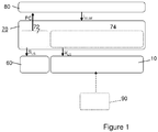
- FIG. 1 schematically shows a dataprocessing apparatus.
- the apparatus comprises a VLIW processor 70 having a vector processing unit 74 that exchanges vector data Vload/Store with a storage facility 10.
- the VLIW processor 70 generates a program counter PC and retrieves VLIW instructions I VLIW from an address in a program memory indicated by the program counter.
- the VLIW processor 70 includes a scalar processing unit 72 that exchanges data S LS with a scalar data memory 60.
- the scalar processor 72 is responsible for generating the program counter PC.
- the data processing apparatus is in particular suitable for processing 2D data, like image data of various nature.
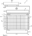
- Figure 2 shows a plurality of access modes for a storage facility.
- a row access mode 10A the storage facility is accessed row-wise.
- access mode a row of elements is simultaneously accessed, i.e. written to or read from the memory.
- This is a common way of data access when the storage facility exchanges data with other facilities, e.g. when data is obtained from a scanner or camera, or when data is provided to a frame buffer.
- column access mode 10B or a block access mode.
- access may be required for example to 4x4 blocks according to access mode 10C, 8x2 blocks according to access mode 10D, or to 2x8 blocks according to access mode 10E.
- a column (10B) may be considered as a 1x16 block.
- FIG 3 shows an embodiment of a storage facility 10 according to the invention in more detail.
- the storage facility 10 is a multimode accessible storage facility in that it allows both row access mode and block access mode.
- the storage facility 10 comprises a memory unit 20 with a plurality of memory banks 20.0, ..., 20.F each having a respective bank index 0,...,F.
- the memory unit comprises 16 banks. It will be understood however that any number NB of banks is possible
- the storage facility 10 further comprises an address generator 30 for generating for each of said memory banks 20.0, ..., 20.F a rotated bank address as a function of an input address and a shift parameter S.
- the storage facility 10 further comprises an input data rotator 40 for rotating an input row by an amount SR and for providing the rotated input row to the memory unit 20.
- the storage facility 10 also comprises an output rotator 50 for inversely rotating a row retrieved from the memory unit 20 by an amount SL and for providing the rotated output row.
- the address generator 30 generates for each of said memory banks 20.0,...20.F a rotated bank address BA(0), ...., BA(F) as a function of an input address Address and a shift parameter SR.
- FIG. 4 schematically shows an embodiment of the address generator 30 in more detail.
- the address generator 30 comprises sections 30.0 to 30.F to generate a rotated bank address for respective banks 20.0 to 20.F dependent on a selected blockwidth BW and multiplexing elements 32.0 to 32.F controlled by a signal S1, that either select the rotated bank address provided by a respective section 30.0 to 30.F or the original address y 0 .
- Figure 5 shows an address generator 130 in another embodiment of the storage facility according to the invention that comprises a first mapping unit 134 for mapping coordinates from a first coordinate system having coordinates X,Y into a second coordinate system having coordinates X*,Y*.
- the X coordinate in the first coordinate system is defined by bits X nx1-1 ,...
- X 0 and the Y coordinate in the first coordinate system is defined by bits Y ny1-1 ,..., Yo and wherein the X* coordinate in the second coordinate system is defined by bits X* nx2-1 ,...,X* 0 and the Y* coordinate in the second coordinate system is defined by bits Y* n y 2-1 ,...,Y* 0 .
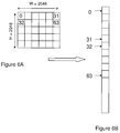
- An example of this address mapping is illustrated with reference to Figure 6A, 6B.
- the image is partitioned into primary cells having a width of 64 pixels and a height of 8 pixels.
- the primary cells are ordered from left to right and from top to bottom. Four of these primary cells are indicated by their number 0, 31, 32, 63.
- the image data is arranged as schematically indicated in Figure 6B .
- Figure 7 shows an exemplary implementation of the address generator 30.
- the address A 0 ,...., A F of each element (x 0 +1, y 0 ), ....( x F +1, y F ) of the block is calculated in block coordinate generator 302.
- the number of elements of the block corresponds to the number of banks of the storage facility.
- a block element may comprise a plurality of pixels. For example 4 pixels of 8 bit may be stored in a single memory bank element of 32 bits. In that case the least significant bits of the x-coordinate may be used to identify a particular pixel within a memory bank element.
- An image may be considered as composed as a number of primary cells, wherein the most significant bits of the x and the y coordinate identify the primary cell of a coordinate and the least significant bits of the x and y coordinate indicate the relative position of the coordinate within that primary cell.
- the rotation of the set of addresses with SRY can be carried out efficiently by a rotator 306 known as such, e.g. by a barrel shifter.
- the bank addresses B I are calculated from addresses A*** I by a second rotation unit 310 by rotation with an amount SRX.
- B I A * * * I ⁇ SRX mod NB SRX is derived from the x0 coordinate of the block within the primary cell.
- nx 2 log NB.
- the input data rotator 40 rotates an input row by an amount SR and provides the rotated input row to the memory unit 20.
- SR WB.y, y being the y coordinate of the row.
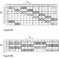
- FIG 8A schematically shows an example, wherein the block width WB is equal to two banks and the number of banks NB is 16. It is further presumed that every bank-address comprises 4 data elements.
- the first row of data elements 0 - 0F, having bank address 0 is stored without rotation, the second row, having bank address 1 is rotated by 2, the third row, having bank address 2 is rotated by 4.
- the block to be read out can be aligned at steps of 4 pixels.
- each next row is rotated by an amount corresponding to the block width WB.
- a row stored at bank address A B is rotated by WB * A B mod NB.
- WB * A B mod NB As each memory bank has a width of 4 pixels this implies that each subsequent row is rotated by 2 banks, which is equivalent to 8 pixels.
- Figure 8B shows how in the same storage facility data may be stored suitable for retrieval in the form of blocks having a width of 16 pixels and a height of 4 pixels. In this case each subsequent row is rotated by 4 banks.
- the storage facility may have different planes.
- a first plane may for example store data for access as 16*4 blocks and another plane may for example store date as 8*8 blocks.
- the rows are rotated by an amount that is a monotonous function of the row number. It is sufficient that separate rows of a block are stored in separate banks. For example a pseudo random function may be used by the input rotator, provided that the inverse function is known by the output rotator.
- the address generator 30 generates for each of the memory banks 20.0, ..., 20.F a rotated bank address as a function of an input address and a shift parameter as follows.
- a B I B y 0 + ⁇ I B WB ⁇ x 0 ⁇ np ⁇ mod NROW
- NROW is the maximum allowable number of rows of a block
- I B is the bank index
- x 0 , y 0 indicates the reference coordinates of the block to be retrieved, e.g. the upper left corner.
- the horizontal position of the block corresponds to the bank index I B of the upper left data element of the block.
- the maximum allowable number of rows NR of a block is the number of banks NB divided by the width WB of a block.
- a first block is shown in light gray in Figure 8A .
- the generated bank addresses B A (I B ) are (y 0 , y 0 , y 0 +1, y 0 +1, ......y 0 +7, y 0 +7).
- the generated bank addresses B A (I B ) are (y 0 +7, y 0 +7, y 0 , y 0 , ....y 0 +6, y 0 +6).
- a data processing apparatus as shown in Figure 1 optionally has a data providing unit 90 (indicated in dashed lines) that provides image data of an image having a width greater than a total datawidth defined by the plurality of memory banks of the storage facility 10. Accordingly an alternative address generator 130 is provided as described with reference to Figure 5 .
- the image providing unit 90 may be a camera or another memory.
- Figure 9 shows a further embodiment of a multimode accessible storage facility 210 according to the invention. Parts therein corresponding to those in Figure 3 have a reference number that is 100 higher.
- the storage facility 210 comprises an address parser 214 that separates the address ADDR provided at the address port into a first set of address lines for identifying an address ADDR1 within the storage facility 210 and a second set of address lines for providing commands CMND to an access mode controller 216.
- the most significant part of the address ADDR forms the command CMND.
- the command is composed of the following fields.
- ⁇ Plane ID (4)> 8 bits, aligned to nibbles
- These fields have the following meaning: Type Value Description Mode (2 bits) - [27:26] Decides the mode of operation 00 Vector Single Addressing 01 2D Addressing 10 reserved 11 Plane Addressing R/B (2 bit) - [25:24] Valid only for 2D mode 00 Row operation on a 2D plane 01 Block operation on a 2D plane Plane ID (4 bits) - [23:20] The values decides which plane is being accessed 00, 01...
- the first command bits determine the access mode.
- the storage facility 210 In the first access mode (vector single addressing) the storage facility 210 is accessible as a conventional memory. Accordingly, the address generator 230 performs no address rotation and the input rotator 240 and the output rotator 250 are inactive.
- the storage space can be subdivided in various parts (here denoted as planes) that have unique properties.
- the plane to be accessed is indicated by the plane ID field. In this case 16 different planes can be defined, but in other embodiments a higher or lower number of planes may be allowed.
- the access mode controller 216 comprises control logic 218 and plane register file 217.
- the settings for each plane may be defined by a respective register in the plane register file 217. These registers may have the following fields.
- each odd line comprises the LUMA components and the subsequent even lines (indicated in gray) comprises the corresponding CHROMA components.
- This interleaving might be required for streaming interfaces which don't generate separate base addresses for each of LUMA / CHROMA component vectors. Blocks for each component type can be retrieved separately by addressing either the odd or the even lines.
- the storage facility comprises a memory with 16 banks. Each memory element comprises 4 vector elements of 16 bits. Not all bits need to be used. In an embodiment for example 9 bits per vector element are used.
- the plane has a storage capacity of 1024 vectors with a length of 64 pixels. In the top left corner some vectors are illustrated by white and gray. I.e. a first vector occupies the addresses 0 to 63. A second vector occupies address 64 to 127, etc.
- Figure 12 further schematically shows the addressability of blocks of pixels within this storage facility.
- the image lines are stored in a rotated fashion in the image memory.
- Each subsequent image line of the primary cell is rotated (shifted cyclically) by a number of banks corresponding to the width Bx of the blocks to be fetched. Due to the fact that each subsequent line is stored in a different set of memory banks, they can be retrieved simultaneously from the memory.
- Various functions of the storage facility may be implemented either in dedicated hardware or by a suitable programmed processor or by a combination of both.
Landscapes
- Engineering & Computer Science (AREA)
- Theoretical Computer Science (AREA)
- Physics & Mathematics (AREA)
- General Physics & Mathematics (AREA)
- Software Systems (AREA)
- General Engineering & Computer Science (AREA)
- Microelectronics & Electronic Packaging (AREA)
- Mathematical Physics (AREA)
- Image Input (AREA)
- Image Processing (AREA)
Claims (8)
- Mehrmoduszugriffsspeichervorrichtung (10), die einen Blockzugriff in einem Blockzugriffsmodus und einen Reihenzugriff in einem Reihenzugriffsmodus erlaubt, wobei die Vorrichtung Folgendes umfasst:- eine Speichereinheit (20), die mehrere Speicherbänke (20.0, ..., 20.F) umfasst, die jeweils einen jeweiligen Bankindex (0, ..., F) aufweisen,- einen Adressengenerator (30) zum Generieren - für jede der Speicherbänke - einer rotierten Bankadresse als eine Funktion einer Eingangsadresse und eines Verschiebungsparameters,- einen Eingangsvektordatenrotator (40) zum Rotieren eines Eingangsvektors und zum Bereitstellen von Vektorelementen des rotierten Eingangsvektors an eine jeweilige Bank der Speichereinheit,- einen Ausgangsvektorrotator (50) zum umgekehrten Rotieren eines Vektors, der Vektorelemente umfasst, die aus jeweiligen Bänken der Speichereinheit abgerufen wurden, und zum Bereitstellen des rotierten Ausgangsvektors;dadurch gekennzeichnet, dass die Speichervorrichtung in mehrere Ebenen unterteilt ist, wobei jede Ebene durch einen jeweiligen gemeinsamen Bereich von Bankadressen in jeder der Speicherbänke definiert wird,
wobei die Speichervorrichtung des Weiteren Folgendes umfasst:- eine Zugriffsmodus-Steuereinheit (216), die eine Ebenenregisterdatei (217) mit einem jeweiligen Register für jede Ebene enthält, das einen Wert umfasst, der eine Blockgröße anzeigt, die für einen blockweisen Datenzugriff gilt,- einen Adressenport mit einem ersten Satz von Adresszeilen zum Identifizieren einer Adresse (ADDR1) innerhalb der Speichervorrichtung und einem zweiten Satz von Adresszeilen zum Bereitstellen von Befehlen (CMND) an die Zugriffsmodus-Steuereinheit (216), wobei der zweite Satz von Adresszeilen Operationsmodus-Anzeigezeilen und/oder Zugriffsmodus-Anzeigezeilen umfasst, wobei der zweite Satz von Adresszeilen des Weiteren Ebenenidentifikationszeilen umfasst. - Mehrmoduszugriffsspeichervorrichtung nach Anspruch 1, wobei der Adressengenerator (130) eine Abbildungseinheit (134) umfasst, um Koordinaten von einem ersten Koordinatensystem, das Koordinaten X,Y aufweist, in ein zweites Koordinatensystem, das Koordinaten X*,Y* aufweist, abzubilden, wobei die X-Koordinate in dem ersten Koordinatensystem durch Bits Xnx1-1, ... , X0 definiert wird und die Y-Koordinate in dem ersten Koordinatensystem durch Bits Yny1-1, ... , Y0 definiert wird, und wobei die X*-Koordinate in dem zweiten Koordinatensystem durch Bits X*nx2-1, ... , X*0 definiert wird und die Y*-Koordinate in dem zweiten Koordinatensystem durch Bits Y*ny2-1, ... , Y*0 definiert wird, wobei der Index 0 das geringstwertige Bit anzeigt, wobei nx1-nx2 = ny2-ny1 = n, und die Abbildungseinheit eine Ausgangsadresse, die eine X*- und eine Y*-Koordinate aufweist, gemäß


- Datenverarbeitungsvorrichtung, die eine Mehrmoduszugriffsspeichervorrichtung (10) nach Anspruch 1 und eine Vektorverarbeitungseinheit (74), die mit der Mehrmoduszugriffsspeichervorrichtung gekoppelt ist, enthält.
- Datenverarbeitungsvorrichtung nach Anspruch 3, die des Weiteren eine Datenbereitstellungseinheit (90) aufweist, die Bilddaten eines Bildes bereitstellt, dessen Breite größer ist als eine Gesamtdatenbreite, die durch die mehreren Speicherbänke definiert wird, wobei der Adressmaskengenerator die Bilddaten von der Datenbereitstellungseinheit als primäre Zellen organisiert, wobei jede primäre Zelle eine Breite aufweist, die der Gesamtdatenbreite entspricht.
- Datenverarbeitungsvorrichtung nach Anspruch 4, wobei die primären Zellen eine Höhe haben, die geringer ist als eine Höhe eines durch die Bilddatenbereitstellungseinheit bereitgestellten Bildes.
- Verfahren zum Speichern einer Reihe von Datenelementen in der Mehrmoduszugriffsspeichervorrichtung nach Anspruch 1, die mehrere Ebenen hat, wobei jede Ebene jeweilige Einstellungen aufweist, wobei das Verfahren folgende Schritte umfasst:- Empfangen der Reihe von Datenelementen,- Empfangen einer Eingangsadresse, die einen Speicherort der Reihe anzeigt, die eine Ebene der mehreren Ebenen anzeigt, und des Weiteren eine Operationsmodusanzeige und/oder einen Zugriffsmodus anzeigt,- Rotieren der Datenelemente jeder nächsten Reihe um einen Betrag, der der Blockbreite WB gemäß den Einstellungen der angezeigten Ebene entspricht,- Zuweisen einer Bankadresse für jedes Element als eine Funktion der Eingangsadresse,- Speichern der Reihe in dem Mehrbankspeicher, wobei jeweilige Datenelemente an einer jeweiligen Bankadresse einer jeweiligen Bank gespeichert werden.
- Verfahren zum Abrufen eines Blocks von Datenelementen aus der Mehrmoduszugriffsspeichervorrichtung nach Anspruch 1, die mehrere Ebenen hat, wobei jede Ebene jeweilige Einstellungen aufweist, wobei das Verfahren folgendes Schritte umfasst:- Empfangen einer Eingangsadresse, die einen Speicherort des Blocks von Datenelementen anzeigt, der eine Ebene der mehreren Ebenen anzeigt, und des Weiteren eine Operationsmodusanzeige und/oder einen Zugriffsmodus anzeigt, und gemäß den Einstellungen für die angezeigte Ebene:- Berechnen einer Bankadresse für mehrere Speicherbänke als eine Funktion der Eingangsadresse,- Abrufen einer Reihe mit jeweiligen Datenelementen aus dem Speicher aus den Bankadressen, die für die Speicherbänke berechnet wurden,- Rotieren der Datenelemente in der Reihe um einen Betrag in Abhängigkeit von dem Speicherort der Reihe und Bereitstellen der Reihe mit den rotierten Datenelementen als den Block.
- Verfahren nach Anspruch 6, wobei der Schritt des Zuweisens einer Bankadresse Folgendes umfasst:- Empfangen einer Eingangsadresse, die erste Daten umfasst, die einen x-Ort in einem Bild anzeigen, und zweite Daten umfasst, die einen y-Ort in einem Bild anzeigen,- Unterteilen der ersten Daten in einen höchstwertigen Teil und einen geringstwertigen Teil,- Zuweisen der Bankadresse auf der Basis des höchstwertigen Teils der ersten Daten und der zweiten Daten.
Applications Claiming Priority (2)
| Application Number | Priority Date | Filing Date | Title |
|---|---|---|---|
| US15416809P | 2009-02-20 | 2009-02-20 | |
| PCT/NL2010/050086 WO2010095944A1 (en) | 2009-02-20 | 2010-02-22 | Multimode accessible storage facility |
Publications (2)
| Publication Number | Publication Date |
|---|---|
| EP2399258A1 EP2399258A1 (de) | 2011-12-28 |
| EP2399258B1 true EP2399258B1 (de) | 2016-04-06 |
Family
ID=42124540
Family Applications (1)
| Application Number | Title | Priority Date | Filing Date |
|---|---|---|---|
| EP10707692.9A Not-in-force EP2399258B1 (de) | 2009-02-20 | 2010-02-22 | In mehreren betriebsarten zugängliche speichereinrichtung |
Country Status (5)
| Country | Link |
|---|---|
| US (1) | US8762686B2 (de) |
| EP (1) | EP2399258B1 (de) |
| JP (1) | JP5552692B2 (de) |
| KR (1) | KR101412392B1 (de) |
| WO (1) | WO2010095944A1 (de) |
Families Citing this family (9)
| Publication number | Priority date | Publication date | Assignee | Title |
|---|---|---|---|---|
| WO2010095944A1 (en) | 2009-02-20 | 2010-08-26 | Silicon Hive B.V. | Multimode accessible storage facility |
| US9329834B2 (en) | 2012-01-10 | 2016-05-03 | Intel Corporation | Intelligent parametric scratchap memory architecture |
| US10467157B2 (en) * | 2015-12-16 | 2019-11-05 | Rambus Inc. | Deterministic operation of storage class memory |
| US11080183B2 (en) * | 2019-08-13 | 2021-08-03 | Elite Semiconductor Memory Technology Inc. | Memory chip, memory module and method for pseudo-accessing memory bank thereof |
| TW202129591A (zh) * | 2019-09-20 | 2021-08-01 | 日商索尼股份有限公司 | 圖像處理裝置及圖像處理方法以及程式 |
| US12175116B2 (en) | 2021-04-27 | 2024-12-24 | Microchip Technology Inc. | Method and apparatus for gather/scatter operations in a vector processor |
| DE112022000529T5 (de) * | 2021-04-27 | 2023-11-16 | Microchip Technology Inc. | Verfahren und vorrichtung für gather/scatter-vorgänge in einem vektorprozessor |
| US11782871B2 (en) | 2021-04-27 | 2023-10-10 | Microchip Technology Inc. | Method and apparatus for desynchronizing execution in a vector processor |
| CN120892358B (zh) * | 2025-07-04 | 2026-03-24 | 摩尔线程智能科技(上海)有限责任公司 | 内存访问请求处理方法、装置、设备、存储介质及程序产品 |
Family Cites Families (13)
| Publication number | Priority date | Publication date | Assignee | Title |
|---|---|---|---|---|
| GB2123998B (en) | 1982-07-21 | 1986-10-22 | Marconi Avionics | Data memory arrangment |
| US4845640A (en) * | 1987-03-11 | 1989-07-04 | Megascan Technology, Inc. | High-speed dual mode graphics memory |
| JP2680208B2 (ja) * | 1991-07-17 | 1997-11-19 | 富士通株式会社 | メモリアクセス制御装置 |
| JP3352755B2 (ja) * | 1993-05-21 | 2002-12-03 | 株式会社リコー | 立体表現画像描画装置 |
| US6031546A (en) * | 1995-06-19 | 2000-02-29 | Canon Kabushiki Kaisha | Image processing apparatus and method |
| JP2000090660A (ja) * | 1998-09-11 | 2000-03-31 | Sony Corp | 記憶装置 |
| WO2000016260A1 (fr) * | 1998-09-11 | 2000-03-23 | Sony Corporation | Processeur de donnees et procede de conversion de sequences de donnees |
| JP3639464B2 (ja) * | 1999-07-05 | 2005-04-20 | 株式会社ルネサステクノロジ | 情報処理システム |
| JP2003084751A (ja) | 2001-07-02 | 2003-03-19 | Hitachi Ltd | 表示制御装置およびマイクロコンピュータならびにグラフィックシステム |
| JP4744510B2 (ja) * | 2004-04-22 | 2011-08-10 | シリコン ハイブ ビー・ヴィー | データ値の多次元アレイへのパラレルなアクセスを提供するデータ処理装置 |
| EP1882235A2 (de) | 2005-05-10 | 2008-01-30 | Nxp B.V. | Bildverarbeitungsschaltung mit blockzugänglichem pufferspeicher |
| US8078830B2 (en) | 2006-05-24 | 2011-12-13 | Nxp B.V. | Processor array accessing data in memory array coupled to output processor with feedback path to input sequencer for storing data in different pattern |
| WO2010095944A1 (en) | 2009-02-20 | 2010-08-26 | Silicon Hive B.V. | Multimode accessible storage facility |
-
2010
- 2010-02-22 WO PCT/NL2010/050086 patent/WO2010095944A1/en not_active Ceased
- 2010-02-22 KR KR1020117021876A patent/KR101412392B1/ko not_active Expired - Fee Related
- 2010-02-22 JP JP2011551027A patent/JP5552692B2/ja not_active Expired - Fee Related
- 2010-02-22 US US13/202,254 patent/US8762686B2/en not_active Expired - Fee Related
- 2010-02-22 EP EP10707692.9A patent/EP2399258B1/de not_active Not-in-force
Also Published As
| Publication number | Publication date |
|---|---|
| JP5552692B2 (ja) | 2014-07-16 |
| US8762686B2 (en) | 2014-06-24 |
| KR101412392B1 (ko) | 2014-06-25 |
| JP2012518831A (ja) | 2012-08-16 |
| EP2399258A1 (de) | 2011-12-28 |
| KR20110121641A (ko) | 2011-11-07 |
| US20120042149A1 (en) | 2012-02-16 |
| WO2010095944A1 (en) | 2010-08-26 |
Similar Documents
| Publication | Publication Date | Title |
|---|---|---|
| EP2399258B1 (de) | In mehreren betriebsarten zugängliche speichereinrichtung | |
| US5111192A (en) | Method to rotate a bitmap image 90 degrees | |
| US8482573B2 (en) | Apparatus and method for processing data | |
| EP0492938A2 (de) | Verfahren und Einrichtung zur Erhöhung der Verarbeitungsgeschwindigkeit eines Anzeigesystems mit Doppel-Pufferspeicher | |
| EP0895216A2 (de) | Bildspeicheranordnungen und Bildzugriffverfahren | |
| KR100804898B1 (ko) | 이미지 회전을 위한 방법 및 장치 | |
| JP3203124B2 (ja) | 画像データ値記憶方式 | |
| CA2058585C (en) | Signal processing system including two-dimensional array transposing | |
| US5613018A (en) | Page buffer rotator | |
| EP1507249A1 (de) | Anzeigesteuerung mit Bilddrehungsfunktion | |
| US6577776B1 (en) | Transforming video images | |
| EP0549316A2 (de) | Dreher für Seitenpuffer | |
| US6573902B1 (en) | Apparatus and method for cache memory connection of texture mapping | |
| US6801209B1 (en) | Method and apparatus for storing data in a block-based memory arrangement | |
| US20080044107A1 (en) | Storage device for storing image data and method of storing image data | |
| US8416252B2 (en) | Image processing apparatus and memory access method thereof | |
| CN101322107A (zh) | 高效访问存储器中的矩阵元素的方法和装置 | |
| CN119360762B (zh) | 对称图像的处理方法、屏显驱动芯片以及显示设备 | |
| KR20000018627A (ko) | 높은 멀티 비트 자유도의 반도체 메모리장치 | |
| US20070040842A1 (en) | Buffer memory system and method | |
| US7457937B1 (en) | Method and system for implementing low overhead memory access in transpose operations | |
| JPH061449B2 (ja) | 画像編集用イメ−ジメモリ | |
| JPS62297951A (ja) | メモリ回路 | |
| JP4696515B2 (ja) | メモリマッピング方法及びメモリインターフェイス回路 | |
| JP2006309776A (ja) | 画像データ記憶装置 |
Legal Events
| Date | Code | Title | Description |
|---|---|---|---|
| PUAI | Public reference made under article 153(3) epc to a published international application that has entered the european phase |
Free format text: ORIGINAL CODE: 0009012 |
|
| 17P | Request for examination filed |
Effective date: 20110919 |
|
| AK | Designated contracting states |
Kind code of ref document: A1 Designated state(s): AT BE BG CH CY CZ DE DK EE ES FI FR GB GR HR HU IE IS IT LI LT LU LV MC MK MT NL NO PL PT RO SE SI SK SM TR |
|
| DAX | Request for extension of the european patent (deleted) | ||
| RAP1 | Party data changed (applicant data changed or rights of an application transferred) |
Owner name: INTEL CORPORATION |
|
| GRAP | Despatch of communication of intention to grant a patent |
Free format text: ORIGINAL CODE: EPIDOSNIGR1 |
|
| REG | Reference to a national code |
Ref country code: DE Ref legal event code: R079 Ref document number: 602010032025 Country of ref document: DE Free format text: PREVIOUS MAIN CLASS: G11C0008040000 Ipc: G06F0009345000 |
|
| INTG | Intention to grant announced |
Effective date: 20150910 |
|
| RIN1 | Information on inventor provided before grant (corrected) |
Inventor name: ALBA PINTO, CARLOS ANTONIO Inventor name: SHARMA, NIKHIL KUMAR |
|
| GRAP | Despatch of communication of intention to grant a patent |
Free format text: ORIGINAL CODE: EPIDOSNIGR1 |
|
| RIC1 | Information provided on ipc code assigned before grant |
Ipc: G06F 9/355 20060101ALI20151005BHEP Ipc: G06F 9/345 20060101AFI20151005BHEP Ipc: G06T 3/60 20060101ALI20151005BHEP |
|
| INTG | Intention to grant announced |
Effective date: 20151111 |
|
| GRAS | Grant fee paid |
Free format text: ORIGINAL CODE: EPIDOSNIGR3 |
|
| GRAA | (expected) grant |
Free format text: ORIGINAL CODE: 0009210 |
|
| AK | Designated contracting states |
Kind code of ref document: B1 Designated state(s): AT BE BG CH CY CZ DE DK EE ES FI FR GB GR HR HU IE IS IT LI LT LU LV MC MK MT NL NO PL PT RO SE SI SK SM TR |
|
| REG | Reference to a national code |
Ref country code: GB Ref legal event code: FG4D |
|
| REG | Reference to a national code |
Ref country code: AT Ref legal event code: REF Ref document number: 788461 Country of ref document: AT Kind code of ref document: T Effective date: 20160415 Ref country code: CH Ref legal event code: EP |
|
| REG | Reference to a national code |
Ref country code: IE Ref legal event code: FG4D |
|
| REG | Reference to a national code |
Ref country code: DE Ref legal event code: R096 Ref document number: 602010032025 Country of ref document: DE |
|
| REG | Reference to a national code |
Ref country code: LT Ref legal event code: MG4D Ref country code: NL Ref legal event code: MP Effective date: 20160406 |
|
| REG | Reference to a national code |
Ref country code: AT Ref legal event code: MK05 Ref document number: 788461 Country of ref document: AT Kind code of ref document: T Effective date: 20160406 |
|
| PG25 | Lapsed in a contracting state [announced via postgrant information from national office to epo] |
Ref country code: NL Free format text: LAPSE BECAUSE OF FAILURE TO SUBMIT A TRANSLATION OF THE DESCRIPTION OR TO PAY THE FEE WITHIN THE PRESCRIBED TIME-LIMIT Effective date: 20160406 |
|
| PG25 | Lapsed in a contracting state [announced via postgrant information from national office to epo] |
Ref country code: PL Free format text: LAPSE BECAUSE OF FAILURE TO SUBMIT A TRANSLATION OF THE DESCRIPTION OR TO PAY THE FEE WITHIN THE PRESCRIBED TIME-LIMIT Effective date: 20160406 Ref country code: LT Free format text: LAPSE BECAUSE OF FAILURE TO SUBMIT A TRANSLATION OF THE DESCRIPTION OR TO PAY THE FEE WITHIN THE PRESCRIBED TIME-LIMIT Effective date: 20160406 Ref country code: IS Free format text: LAPSE BECAUSE OF FAILURE TO SUBMIT A TRANSLATION OF THE DESCRIPTION OR TO PAY THE FEE WITHIN THE PRESCRIBED TIME-LIMIT Effective date: 20160806 Ref country code: FI Free format text: LAPSE BECAUSE OF FAILURE TO SUBMIT A TRANSLATION OF THE DESCRIPTION OR TO PAY THE FEE WITHIN THE PRESCRIBED TIME-LIMIT Effective date: 20160406 Ref country code: NO Free format text: LAPSE BECAUSE OF FAILURE TO SUBMIT A TRANSLATION OF THE DESCRIPTION OR TO PAY THE FEE WITHIN THE PRESCRIBED TIME-LIMIT Effective date: 20160706 |
|
| PG25 | Lapsed in a contracting state [announced via postgrant information from national office to epo] |
Ref country code: AT Free format text: LAPSE BECAUSE OF FAILURE TO SUBMIT A TRANSLATION OF THE DESCRIPTION OR TO PAY THE FEE WITHIN THE PRESCRIBED TIME-LIMIT Effective date: 20160406 Ref country code: HR Free format text: LAPSE BECAUSE OF FAILURE TO SUBMIT A TRANSLATION OF THE DESCRIPTION OR TO PAY THE FEE WITHIN THE PRESCRIBED TIME-LIMIT Effective date: 20160406 Ref country code: LV Free format text: LAPSE BECAUSE OF FAILURE TO SUBMIT A TRANSLATION OF THE DESCRIPTION OR TO PAY THE FEE WITHIN THE PRESCRIBED TIME-LIMIT Effective date: 20160406 Ref country code: ES Free format text: LAPSE BECAUSE OF FAILURE TO SUBMIT A TRANSLATION OF THE DESCRIPTION OR TO PAY THE FEE WITHIN THE PRESCRIBED TIME-LIMIT Effective date: 20160406 Ref country code: SE Free format text: LAPSE BECAUSE OF FAILURE TO SUBMIT A TRANSLATION OF THE DESCRIPTION OR TO PAY THE FEE WITHIN THE PRESCRIBED TIME-LIMIT Effective date: 20160406 Ref country code: GR Free format text: LAPSE BECAUSE OF FAILURE TO SUBMIT A TRANSLATION OF THE DESCRIPTION OR TO PAY THE FEE WITHIN THE PRESCRIBED TIME-LIMIT Effective date: 20160707 Ref country code: PT Free format text: LAPSE BECAUSE OF FAILURE TO SUBMIT A TRANSLATION OF THE DESCRIPTION OR TO PAY THE FEE WITHIN THE PRESCRIBED TIME-LIMIT Effective date: 20160808 |
|
| PG25 | Lapsed in a contracting state [announced via postgrant information from national office to epo] |
Ref country code: BE Free format text: LAPSE BECAUSE OF FAILURE TO SUBMIT A TRANSLATION OF THE DESCRIPTION OR TO PAY THE FEE WITHIN THE PRESCRIBED TIME-LIMIT Effective date: 20160406 Ref country code: IT Free format text: LAPSE BECAUSE OF FAILURE TO SUBMIT A TRANSLATION OF THE DESCRIPTION OR TO PAY THE FEE WITHIN THE PRESCRIBED TIME-LIMIT Effective date: 20160406 |
|
| REG | Reference to a national code |
Ref country code: DE Ref legal event code: R097 Ref document number: 602010032025 Country of ref document: DE |
|
| PG25 | Lapsed in a contracting state [announced via postgrant information from national office to epo] |
Ref country code: RO Free format text: LAPSE BECAUSE OF FAILURE TO SUBMIT A TRANSLATION OF THE DESCRIPTION OR TO PAY THE FEE WITHIN THE PRESCRIBED TIME-LIMIT Effective date: 20160406 Ref country code: CZ Free format text: LAPSE BECAUSE OF FAILURE TO SUBMIT A TRANSLATION OF THE DESCRIPTION OR TO PAY THE FEE WITHIN THE PRESCRIBED TIME-LIMIT Effective date: 20160406 Ref country code: EE Free format text: LAPSE BECAUSE OF FAILURE TO SUBMIT A TRANSLATION OF THE DESCRIPTION OR TO PAY THE FEE WITHIN THE PRESCRIBED TIME-LIMIT Effective date: 20160406 Ref country code: DK Free format text: LAPSE BECAUSE OF FAILURE TO SUBMIT A TRANSLATION OF THE DESCRIPTION OR TO PAY THE FEE WITHIN THE PRESCRIBED TIME-LIMIT Effective date: 20160406 Ref country code: SK Free format text: LAPSE BECAUSE OF FAILURE TO SUBMIT A TRANSLATION OF THE DESCRIPTION OR TO PAY THE FEE WITHIN THE PRESCRIBED TIME-LIMIT Effective date: 20160406 |
|
| PLBE | No opposition filed within time limit |
Free format text: ORIGINAL CODE: 0009261 |
|
| STAA | Information on the status of an ep patent application or granted ep patent |
Free format text: STATUS: NO OPPOSITION FILED WITHIN TIME LIMIT |
|
| PG25 | Lapsed in a contracting state [announced via postgrant information from national office to epo] |
Ref country code: SM Free format text: LAPSE BECAUSE OF FAILURE TO SUBMIT A TRANSLATION OF THE DESCRIPTION OR TO PAY THE FEE WITHIN THE PRESCRIBED TIME-LIMIT Effective date: 20160406 |
|
| 26N | No opposition filed |
Effective date: 20170110 |
|
| PG25 | Lapsed in a contracting state [announced via postgrant information from national office to epo] |
Ref country code: SI Free format text: LAPSE BECAUSE OF FAILURE TO SUBMIT A TRANSLATION OF THE DESCRIPTION OR TO PAY THE FEE WITHIN THE PRESCRIBED TIME-LIMIT Effective date: 20160406 |
|
| PG25 | Lapsed in a contracting state [announced via postgrant information from national office to epo] |
Ref country code: MC Free format text: LAPSE BECAUSE OF FAILURE TO SUBMIT A TRANSLATION OF THE DESCRIPTION OR TO PAY THE FEE WITHIN THE PRESCRIBED TIME-LIMIT Effective date: 20160406 |
|
| REG | Reference to a national code |
Ref country code: CH Ref legal event code: PL |
|
| PG25 | Lapsed in a contracting state [announced via postgrant information from national office to epo] |
Ref country code: CH Free format text: LAPSE BECAUSE OF NON-PAYMENT OF DUE FEES Effective date: 20170228 Ref country code: LI Free format text: LAPSE BECAUSE OF NON-PAYMENT OF DUE FEES Effective date: 20170228 |
|
| REG | Reference to a national code |
Ref country code: IE Ref legal event code: MM4A |
|
| REG | Reference to a national code |
Ref country code: FR Ref legal event code: ST Effective date: 20171031 |
|
| PG25 | Lapsed in a contracting state [announced via postgrant information from national office to epo] |
Ref country code: LU Free format text: LAPSE BECAUSE OF NON-PAYMENT OF DUE FEES Effective date: 20170222 |
|
| PG25 | Lapsed in a contracting state [announced via postgrant information from national office to epo] |
Ref country code: FR Free format text: LAPSE BECAUSE OF NON-PAYMENT OF DUE FEES Effective date: 20170228 |
|
| PG25 | Lapsed in a contracting state [announced via postgrant information from national office to epo] |
Ref country code: IE Free format text: LAPSE BECAUSE OF NON-PAYMENT OF DUE FEES Effective date: 20170222 |
|
| PGFP | Annual fee paid to national office [announced via postgrant information from national office to epo] |
Ref country code: DE Payment date: 20180206 Year of fee payment: 9 Ref country code: GB Payment date: 20180221 Year of fee payment: 9 |
|
| PG25 | Lapsed in a contracting state [announced via postgrant information from national office to epo] |
Ref country code: MT Free format text: LAPSE BECAUSE OF NON-PAYMENT OF DUE FEES Effective date: 20170222 |
|
| PG25 | Lapsed in a contracting state [announced via postgrant information from national office to epo] |
Ref country code: HU Free format text: LAPSE BECAUSE OF FAILURE TO SUBMIT A TRANSLATION OF THE DESCRIPTION OR TO PAY THE FEE WITHIN THE PRESCRIBED TIME-LIMIT; INVALID AB INITIO Effective date: 20100222 |
|
| PG25 | Lapsed in a contracting state [announced via postgrant information from national office to epo] |
Ref country code: BG Free format text: LAPSE BECAUSE OF FAILURE TO SUBMIT A TRANSLATION OF THE DESCRIPTION OR TO PAY THE FEE WITHIN THE PRESCRIBED TIME-LIMIT Effective date: 20160406 |
|
| REG | Reference to a national code |
Ref country code: DE Ref legal event code: R119 Ref document number: 602010032025 Country of ref document: DE |
|
| GBPC | Gb: european patent ceased through non-payment of renewal fee |
Effective date: 20190222 |
|
| PG25 | Lapsed in a contracting state [announced via postgrant information from national office to epo] |
Ref country code: CY Free format text: LAPSE BECAUSE OF NON-PAYMENT OF DUE FEES Effective date: 20160406 |
|
| PG25 | Lapsed in a contracting state [announced via postgrant information from national office to epo] |
Ref country code: MK Free format text: LAPSE BECAUSE OF FAILURE TO SUBMIT A TRANSLATION OF THE DESCRIPTION OR TO PAY THE FEE WITHIN THE PRESCRIBED TIME-LIMIT Effective date: 20160406 |
|
| PG25 | Lapsed in a contracting state [announced via postgrant information from national office to epo] |
Ref country code: DE Free format text: LAPSE BECAUSE OF NON-PAYMENT OF DUE FEES Effective date: 20190903 Ref country code: GB Free format text: LAPSE BECAUSE OF NON-PAYMENT OF DUE FEES Effective date: 20190222 |
|
| PG25 | Lapsed in a contracting state [announced via postgrant information from national office to epo] |
Ref country code: TR Free format text: LAPSE BECAUSE OF FAILURE TO SUBMIT A TRANSLATION OF THE DESCRIPTION OR TO PAY THE FEE WITHIN THE PRESCRIBED TIME-LIMIT Effective date: 20160406 |