EP2398086A1 - Opto-electric device and method of manufacturing thereof - Google Patents
Opto-electric device and method of manufacturing thereof Download PDFInfo
- Publication number
- EP2398086A1 EP2398086A1 EP20100166379 EP10166379A EP2398086A1 EP 2398086 A1 EP2398086 A1 EP 2398086A1 EP 20100166379 EP20100166379 EP 20100166379 EP 10166379 A EP10166379 A EP 10166379A EP 2398086 A1 EP2398086 A1 EP 2398086A1
- Authority
- EP
- European Patent Office
- Prior art keywords
- layer
- opto
- electrically conductive
- conductive layer
- electric
- Prior art date
- Legal status (The legal status is an assumption and is not a legal conclusion. Google has not performed a legal analysis and makes no representation as to the accuracy of the status listed.)
- Withdrawn
Links
Images


Classifications
-
- H—ELECTRICITY
- H10—SEMICONDUCTOR DEVICES; ELECTRIC SOLID-STATE DEVICES NOT OTHERWISE PROVIDED FOR
- H10K—ORGANIC ELECTRIC SOLID-STATE DEVICES
- H10K50/00—Organic light-emitting devices
- H10K50/80—Constructional details
- H10K50/805—Electrodes
- H10K50/82—Cathodes
- H10K50/824—Cathodes combined with auxiliary electrodes
-
- H—ELECTRICITY
- H10—SEMICONDUCTOR DEVICES; ELECTRIC SOLID-STATE DEVICES NOT OTHERWISE PROVIDED FOR
- H10K—ORGANIC ELECTRIC SOLID-STATE DEVICES
- H10K71/00—Manufacture or treatment specially adapted for the organic devices covered by this subclass
- H10K71/621—Providing a shape to conductive layers, e.g. patterning or selective deposition
-
- H—ELECTRICITY
- H10—SEMICONDUCTOR DEVICES; ELECTRIC SOLID-STATE DEVICES NOT OTHERWISE PROVIDED FOR
- H10H—INORGANIC LIGHT-EMITTING SEMICONDUCTOR DEVICES HAVING POTENTIAL BARRIERS
- H10H20/00—Individual inorganic light-emitting semiconductor devices having potential barriers, e.g. light-emitting diodes [LED]
- H10H20/80—Constructional details
- H10H20/83—Electrodes
-
- H—ELECTRICITY
- H10—SEMICONDUCTOR DEVICES; ELECTRIC SOLID-STATE DEVICES NOT OTHERWISE PROVIDED FOR
- H10K—ORGANIC ELECTRIC SOLID-STATE DEVICES
- H10K50/00—Organic light-emitting devices
- H10K50/10—OLEDs or polymer light-emitting diodes [PLED]
- H10K50/17—Carrier injection layers
-
- H—ELECTRICITY
- H10—SEMICONDUCTOR DEVICES; ELECTRIC SOLID-STATE DEVICES NOT OTHERWISE PROVIDED FOR
- H10K—ORGANIC ELECTRIC SOLID-STATE DEVICES
- H10K50/00—Organic light-emitting devices
- H10K50/80—Constructional details
- H10K50/805—Electrodes
-
- H—ELECTRICITY
- H10—SEMICONDUCTOR DEVICES; ELECTRIC SOLID-STATE DEVICES NOT OTHERWISE PROVIDED FOR
- H10K—ORGANIC ELECTRIC SOLID-STATE DEVICES
- H10K50/00—Organic light-emitting devices
- H10K50/80—Constructional details
- H10K50/805—Electrodes
- H10K50/81—Anodes
-
- H—ELECTRICITY
- H10—SEMICONDUCTOR DEVICES; ELECTRIC SOLID-STATE DEVICES NOT OTHERWISE PROVIDED FOR
- H10K—ORGANIC ELECTRIC SOLID-STATE DEVICES
- H10K50/00—Organic light-emitting devices
- H10K50/80—Constructional details
- H10K50/805—Electrodes
- H10K50/82—Cathodes
-
- H—ELECTRICITY
- H10—SEMICONDUCTOR DEVICES; ELECTRIC SOLID-STATE DEVICES NOT OTHERWISE PROVIDED FOR
- H10K—ORGANIC ELECTRIC SOLID-STATE DEVICES
- H10K50/00—Organic light-emitting devices
- H10K50/80—Constructional details
- H10K50/805—Electrodes
- H10K50/82—Cathodes
- H10K50/828—Transparent cathodes, e.g. comprising thin metal layers
-
- H—ELECTRICITY
- H10—SEMICONDUCTOR DEVICES; ELECTRIC SOLID-STATE DEVICES NOT OTHERWISE PROVIDED FOR
- H10K—ORGANIC ELECTRIC SOLID-STATE DEVICES
- H10K71/00—Manufacture or treatment specially adapted for the organic devices covered by this subclass
-
- H—ELECTRICITY
- H10—SEMICONDUCTOR DEVICES; ELECTRIC SOLID-STATE DEVICES NOT OTHERWISE PROVIDED FOR
- H10K—ORGANIC ELECTRIC SOLID-STATE DEVICES
- H10K71/00—Manufacture or treatment specially adapted for the organic devices covered by this subclass
- H10K71/10—Deposition of organic active material
-
- H—ELECTRICITY
- H10—SEMICONDUCTOR DEVICES; ELECTRIC SOLID-STATE DEVICES NOT OTHERWISE PROVIDED FOR
- H10K—ORGANIC ELECTRIC SOLID-STATE DEVICES
- H10K71/00—Manufacture or treatment specially adapted for the organic devices covered by this subclass
- H10K71/60—Forming conductive regions or layers, e.g. electrodes
-
- H—ELECTRICITY
- H10—SEMICONDUCTOR DEVICES; ELECTRIC SOLID-STATE DEVICES NOT OTHERWISE PROVIDED FOR
- H10K—ORGANIC ELECTRIC SOLID-STATE DEVICES
- H10K2102/00—Constructional details relating to the organic devices covered by this subclass
- H10K2102/301—Details of OLEDs
- H10K2102/302—Details of OLEDs of OLED structures
- H10K2102/3023—Direction of light emission
- H10K2102/3026—Top emission
-
- H—ELECTRICITY
- H10—SEMICONDUCTOR DEVICES; ELECTRIC SOLID-STATE DEVICES NOT OTHERWISE PROVIDED FOR
- H10K—ORGANIC ELECTRIC SOLID-STATE DEVICES
- H10K2102/00—Constructional details relating to the organic devices covered by this subclass
- H10K2102/301—Details of OLEDs
- H10K2102/351—Thickness
-
- H—ELECTRICITY
- H10—SEMICONDUCTOR DEVICES; ELECTRIC SOLID-STATE DEVICES NOT OTHERWISE PROVIDED FOR
- H10K—ORGANIC ELECTRIC SOLID-STATE DEVICES
- H10K50/00—Organic light-emitting devices
- H10K50/10—OLEDs or polymer light-emitting diodes [PLED]
- H10K50/17—Carrier injection layers
- H10K50/171—Electron injection layers
Definitions
- the present invention relates to an opto-electric device.
- the present invention further relates to a method of manufacturing an opto-electric device.
- An opto-electric device is a device that provides for an optical effect in response to an electric signal, or that generates an electric signal in response to an optical stimulus.
- Examples of the first are light emitting diodes, such as organic light emitting diodes.
- various photoactive materials are known that convert an electric current into photon radiation.
- Photoactive materials may typically be any organic electroluminescent (“EL") material, including, but not limited to, small molecule organic fluorescent compounds, fluorescent and phosphorescent metal complexes, conjugated polymers, and combinations or mixtures thereof.
- EL organic electroluminescent
- fluorescent compounds include, but are not limited to, pyrene, perylene, rubrene, coumarin, derivatives thereof, and mixtures thereof.
- metal complexes include, but are not limited to, metal chelated oxinoid compounds, such as tris(8-hydroxyquinolato)aluminum (Alq3); cyclometalated iridium and platinum electroluminescent compounds, such as complexes of iridium with phenylpyridine, phenylquinoline, or phenylpyrimidine ligands as disclosed in Petrov et al., U.S. Pat. No.
- metal chelated oxinoid compounds such as tris(8-hydroxyquinolato)aluminum (Alq3)
- cyclometalated iridium and platinum electroluminescent compounds such as complexes of iridium with phenylpyridine, phenylquinoline, or phenylpyrimidine ligands as disclosed in Petrov et al., U.S. Pat. No.
- Electroluminescent emissive layers comprising a charge carrying host material and a metal complex have been described by Thompson et al., in U.S. Pat. No. 6,303,238 , and by Burrows and Thompson in published PCT applications WO 00/70655 and WO 01/41512 .
- conjugated polymers include, but are not limited to poly(phenylenevinylenes), polyfluorenes, poly(spirobifluorenes), polythiophenes, poly(p-phenylenes), copolymers thereof, and may further include combinations or mixtures thereof.
- the choice of a particular material may depend on the specific application, potentials used during operation, or other factors.
- the present thin film materials used for the semitransparent electrode e.g. ITO
- ITO the semitransparent electrode
- the conductivity of the electrode layers could be improved by increasing their thickness.
- the thickness of the transparent electrode layer cannot be increased too much in order to avoid an unacceptably low transparency.
- the transparent electrode should transmit a substantial amount, i.e. at least 50%, preferably at least 80% of photon radiation impingent thereon. This can be photon radiation rendered by the opto-electric layer for transmission to outside the device, or can be photon radiation from outside the device for transmission to the opto-electric layer.
- WO2007/036850 describes an organic diode device that comprises an organic diode structure having an anode layer, a cathode layer and an organic layer. At least one of the anode layer and the cathode layer has a set of contact areas that are distributed over a face of said structure.
- a barrier layer hermetically covers said structure and is provided with a set of openings aligned with said set of contact areas.
- a metal conductor has been electroplated on said barrier layer and contacts the set of contact areas via the set of openings.
- the electroplated metal conductor shunts the anode and the cathode, and therewith provides for an even voltage distribution over the area of a large organic diode device and therewith an even luminance.
- a "layer" of a given material includes a region of that material whose thickness is small compared to both its length and width. Examples of layers include sheets, foils, films, laminations, coatings, and so forth. As used herein a layer need not be planar, but can be bent, folded or otherwise contoured, for example, to at least partially envelop another component. As used herein a layer can also include multiple sub-layers. A layer can also consist of a collection of discrete portions, for example, a layer of discrete active regions comprising individual pixels.
- the anode is an electrode that is particularly efficient for injecting positive charge carriers. It can be made of, for example materials containing a metal, mixed metal, alloy, metal oxide or mixed-metal oxide, or it can be a conducting polymer, and mixtures thereof. Suitable metals include the Group 11 metals, the metals in Groups 4, 5, and 6, and the Group 8-10 transition metals. If the anode is to be light-transmitting, mixed-metal oxides of Groups 12, 13 and 14 metals, such as indium-tin- oxide, are generally used.
- the anode may also comprise an organic material such as polyaniline as described in " Flexible light-emitting diodes made from soluble conducting polymer," Nature vol. 357, pp 477479 (11 June 1992 ). At least one of the anode and cathode should be at least partially transparent to allow the generated light to be observed. In the case where the transparent electrode is the electrode facing a substrate of the device the substrate must also then be transparent. In the case where the whole device has to be transparent, each of the layers within the device and the substrate have to be transparent
- the electrode having the lowest work-function serves as the cathode.
- a material is considered to have a low work-function if it has a work function not greater than about 4.4 eV.
- metals or nonmetals may be used.
- Materials for the cathode layer can be selected from alkali metals of Group 1 (e.g., Li, Na, K, Rb, Cs,), the Group 2 metals (e.g., Mg, Ca, Ba, or the like), the Group 12 metals, the lanthanides (e.g., Ce, Sm, Eu, or the like), and the actinides (e.g., Th, U, or the like).
- the cathode layer may be formed as a combination of sub-layers, e.g. a layer of Ba having a thickness of about 5 nm facing the towards the opto-electric layer combined with a layer of aluminium having a thickness in the range of 10-400 nm facing away from the opto-electric layer.
- the second electrode layer has to be applied in a conditioned, i.e. an inert or a vacuum environment to prevent such corrosion.
- the cathode layer is usually formed by a chemical or physical vapor deposition process.
- subsequent layers and other features have to be deposited in a conditioned environment as oxygen or water vapor could reach the deposited electrode directly or through diffusion via the already deposited layers.
- the patterned electrically conductive layer is deposited before the deposition of the transparent electrode, there are no limitations in this respect on the deposition method to be used for the patterned electrically conductive layer. It is for example not necessary that the patterned electrically conductive layer is applied in a conditioned environment. This facilitates using a deposition method suitable for large scale manufacturing, e.g. suitable for roll to roll processing. Examples of deposition processes suitable for use in a roll to roll process are ink-jet printing and screen printing.
- inkjet printing is used as the printing method.
- patterned electrically conductive layer Various materials are possible for use as the patterned electrically conductive layer and may be applied accordingly.
- the patterned electrically conductive layer may for example be of a metal or a metal alloy that is applied in liquid form by inkjet printing.
- Various metals and metal alloys are available that have a relatively low melting point or melting trajectory.
- the skilled person may select the most suitable metal or metal alloy from a variety of metals and metal alloys.
- the skilled person may select for example from commercially available, low cost, low-melting metals and metal alloys. These may comprise for example elements selected from the group consisting of In, Sn, Bi, Pb, Hg, Ga and Cd.
- said metals also offer a broad spectrum of other properties which are important, such as sensitivity to oxidation, adhesion to other materials, coefficient of thermal expansion, ductility, dimensional stability, degree of shrinkage upon solidification and wetting.
- alloys containing Hg or Cd such as Sn: (50 wt. %): Pb (32 wt. %): Cd (18 wt. %) alloy are not to be preferred.
- a ductile low-melting metal such as indium (melting point 157 C) or Sn (35.7 wt. %): Bi (35.7 wt. %): Pb (28. 6 wt. %), which has a melting point of 100 C.
- a metal which, upon solidification, does not form crystalline domains and exhibits little shrinkage such as Bi (58 wt. %): Sn (42 wt. %), melting point 138 C, is preferred.
- the patterned electrically conductive layer may be applied in the form of suspension or colloidal solution of metal particles or organic metal complexes.
- the suspension or colloidal solution may be applied by means of ink jet printing.
- suspension or colloidal solution to be printed may be heated to facilitate the printing process, for example in a range between 100 and 300 °C.
- Nanoparticles from silver, copper, platinum and/or gold or organic metal complexes may be used in the suspension or colloidal solution to the formation of the auxiliary conductive strip.
- the nanoparticles preferably exhibit a diameter between 1 nm and 100 nm.
- the used ink can be also a colloidal solution.
- An example thereof is a silver nanoparticle dispersion in an ethylene glycol/ethanol mixture as provided by Cabot (Cabot Printing Electronics and Displays, USA).
- This silver ink contains 20 wt% of silver nanoparticles, with the particle diameter ranging from 30 to 50 nm.
- the viscosity and surface tension of this ink is 14.4 mPa.s and 31 mN m -1 , respectively.
- Metal complexes in organic or water based solvents may be used as the substance.
- Metal complexes may comprise organic silver, copper, platinum or gold complexes or of a mixture of these complexes.
- silver complex inks may be used comprising a mixture of solvents and silver amides, for example inks produced by InkTec. The silver amides decompose at a certain temperature between 130-150°C into silver atoms, volatile amines and carbon dioxide. Once the solvents and the amines are evaporated, the silver atoms remain on the substrate.
- Other metal complexes based for example on copper, nickel, zinc, cobalt, palladium, gold, vanadium, and bismuth instead of silver may be used alternatively or in combination.
- metal complexes based for example on copper, nickel, zinc, aluminum, cobalt, palladium, gold, vanadium, and bismuth instead of silver may be used alternatively or in combination.
- particularly suitable are a silver complex, a copper complex, a nickel-complex, an aluminum-complex or any mixture thereof.
- Silver, copper, aluminum and nickel are excellent conductors.
- Table 1 Examples of substances comprising a Cu-complex component Cu(neodecanoate)2 (6-12% Cu; from Strem Chemicals) Cu(acetate)2.H2O (from Sigma Aldrich) complex with ethanolamine is soluble in water (concentration N/A) Cu(formate) 2.4 H2O (from Gelest)
- the patterned electrically conductive layer may alternatively be a conductive polymer structure.
- a structure can be formed from a substance that comprises conductive polymer particles, for example suspended in a liquid.
- electrically conductive polymers are poly-(3,4-ethylenedioxythiophene) (PEDOT) or polyaniline (PANI).
- PEDOT poly-(3,4-ethylenedioxythiophene)
- PANI polyaniline
- a substance comprising a suspension of particles of a precursor for a conductive polymer may be used.
- metals or alloys thereof e.g. deposited in the form of a suspension
- they have a relatively good conductivity in comparison to organic substances.
- a solution with molecular metal precursors, and/or with conductive organic compounds, and/or with a precursor for a conductive organic compound may be deposited to form the patterned electrically conductive layer.
- Typical mean particle diameters are in a range between 1 nm and 100 ⁇ m, preferably 1 nm ⁇ 1 ⁇ m, very preferred 1 nm ⁇ 100 nm and especially preferred 1 nm — 50 nm.
- the mean particle diameter can be determined by transmission electron microscope (TEM).
- TEM transmission electron microscope
- Very suitable are metal nanoparticles as they allow the formation of conducting surface patterns with a minimum amount of electromagnetic energy.
- the suspension or colloidal solution may be printed in a narrow line structure if the surface of the opto-electric layer is prepared with a surface energy modifying agent.
- a surface energy modifying agent Dependent on the surface energy in of the surface where the suspension or colloidal solution is applied, contact angles in the range of 30 deg to 60 deg may be realized.
- the inkjet printer used may eject the substance to be printed in the form of drops that merge into a continuous pattern, or may print a continuous beam of the substance to be printed at the surface. In an embodiment the process of printing is repeated. Therewith a relative high aspect ratio (height/width ratio) of the printed pattern can be achieved.
- An embodiment of the method according to the first aspect further comprises the step of locally depositing an insulating material onto the opto-electric layer in a pattern at least substantially conformal to the pattern to be formed by the patterned electrically conductive layer.
- the wording "at least substantially conformal” is understood to mean that the pattern of the insulating layer is conformal to that of the patterned electrically conductive layer or that the features of the insulating layer laterally extend beyond the features formed by the patterned electrically conductive layer.
- the features of the patterns are lineshaped, and the lineshaped features of the insulating layer should not extend laterally more than by 20% of the width of the lineshaped features of the patterned electrically conductive layer.
- the insulating layer may be formed from a resin material such as an acrylate and is deposited by using a technique which allows patterning such as inkjet printing or screen printing.
- the thickness of this material may be between 1 and 20 ⁇ m and should have a cross-sectional profile such that the deposited cathode can make electrical contact to both the deposited patterned electrically conductive layer and the opto-electric layer.
- the opto-electric device may be flexible or rigid.
- the opto-electric device may be arranged in a housing that provides protection for moisture and oxygen.
- the housing may include a getter material.
- the opto-electric device may be provided with one or more barrier layers for protection against moisture and oxygen.
- a barrier layer typically comprises a stack of sub-layers.
- the barrier layer is a stack comprising an organic layer sandwiched between a first and a second inorganic layer.
- the stack may comprise further organic and inorganic layers that alternate each other.
- the organic layers may comprise a moisture getter.
- a barrier layer may comprise a stack of layers of different inorganic materials that alternate each other.
- the opto-electric device may be applied on a substrate that has barrier functionality, e.g. a substrate of glass or of aluminium or stainless steel.
- an opto-electric device having a stack of layers subsequently comprising
- the patterned electrically conductive layer is arranged between the opto-electric layer and the transparent electrically conductive layer forming the electrode having the lower workfunction.
- the transparent electrically conductive layer of the material having the relatively low work function is in practice arranged at a side opposite the side of the substrate.
- the opto-electric device may be removed from the substrate after completion of the manufacturing process. Accordingly, if the opto-electric layer in the device according to the second aspect of the invention is an electroluminescent layer (EL) the device according to the invention is a so-called top-emissive OLED. Nevertheless the device according to the invention may have in addition a first electrode that is transparent and that is shunted by an additional patterned electrically conductive layer.
- EL electroluminescent layer
- the opto-electric device according the second aspect of the present invention can be manufactured by the method according to the first aspect of the invention.
- the first electrode layer may form the anode and the second (transparent) electrode layer may form the cathode or the other way around.
- the device may have one or more optional buffer layers comprises buffer materials.
- buffer layer or “buffer material” is intended to mean electrically conductive or semiconductive materials and may have one or more functions in an organic electronic device, including but not limited to, planarization of the underlying layer, charge transport and/or charge injection properties, scavenging of impurities such as oxygen or metal ions, and other aspects to facilitate or to improve the performance of the organic electronic device.
- Buffer materials may be polymers, oligomers, or small molecules, and may be in the form of solutions, dispersions, suspensions, emulsions, colloidal mixtures, or other compositions.
- the buffer layer can be formed with polymeric materials, such as polyaniline (PANI) or poiyethylenedioxythiophene (PEDOT), which are often doped with protonic acids.
- the protonic acids can be, for example, poly(styrenesulfontc acid), poly ⁇ 2-acrylamido-2-methyl-1-propanesulfonic acid), and the like.
- the buffer layer can comprise charge transfer compounds, and the like, such as copper phthalocyanine and the tetrathiafulvalene-tetracyanoquinodimethane system (TTF-TCNQ).
- the opto-electric device may comprise a hole injection and/or transport layer (HTL) between the electrode layer forming the anode and the opto-electric layer and/or an electron injection and/or transport layer (ETL) between the electrode layer forming the cathode and the opto-electric layer.
- HTL hole injection and/or transport layer
- ETL electron injection and/or transport layer
- the patterned electrically conductive layer should be present between the electron transport layer and the cathode.
- hole transport materials for the hole transport layer have been summarized for example, in Kirk-Othmer Encyclopedia of Chemical Technology, Fourth Edition, Vol. 18, p. 837-860, 1996, by Y. Wang . Both hole transporting molecules and polymers can be used. Commonly used hole transporting molecules include, but are not limited to: 4,4',4"-tris(N,N-diphenyl-amino)-triphenylamine (TDATA); 4,4',4"-tris(N-3-methylphenyl-N-phenyl-amino)-triphenylamine (MTDATA); N,N'-diphenyl-N,N'-bis(3-methylphenyl)-[1,1'-biphenyl]-4,4'-diamine (TPD); 1,1-bis[(di-4-tolylamino) phenyl]cyclohexane (TAPC); N,N'-bis(4-methylphenyl)-N,N'-bis(4-ethylphen
- hole transporting polymers include, but are not limited to, poly(9,9,-dioctyl-fluorene-co-N-(4-butylphenyl)diphenylamine), and the like, polyvinylcarbazole, (phenylmethyl)polysilane, poly(dioxythiophenes), polyanilines, and polypyrroles.
- Another example is polyethylene dioxythiophene (PEDOT). It is also possible to obtain hole transporting polymers by doping hole transporting molecules such as those mentioned above into polymers such as polystyrene and polycarbonate.
- the electron transport layer can function both to facilitate electron transport, and also serve as a buffer layer or confinement layer to prevent quenching of the exciton at layer interfaces. Preferably, this layer promotes electron mobility and reduces exciton quenching.
- electron transport materials which can be used in the optional electron transport layer, include metal chelated oxinoid compounds, including metal quinolate derivatives such as tris(8-hydroxyquinoiato)aluminum (AIQ), bis(2-methyl-8-quino!inolato)(p-phenyiphenolato) aluminum (BAIq).
- an embodiment of the opto-electric device comprises a sequence of layers including an anode layer, HTL (layer), opto-electric layer, cathode.
- Another embodiment comprises anode, opto-electric layer, ETL (layer), cathode.
- another embodiment comprises anode, hole-transport layer, opto-electric layer, ETL (layer), cathode.
- first, second, third etc. may be used herein to describe various elements, components, regions, layers and/or sections, these elements, components, regions, layers and/or sections should not be limited by these terms. These terms are only used to distinguish one element, component, region, layer or section from another region, layer or section. Thus, a first element, component, region, layer or section discussed below could be termed a second element, component, region, layer or section without departing from the teachings of the present invention.
- Embodiments of the invention are described herein with reference to cross-section illustrations that are schematic illustrations of idealized embodiments (and intermediate structures) of the invention. As such, variations from the shapes of the illustrations as a result, for example, of manufacturing techniques and/or tolerances, are to be expected. Thus, embodiments of the invention should not be construed as limited to the particular shapes of regions illustrated herein but are to include deviations in shapes that result, for example, from manufacturing.
- FIG. 1 schematically shows a first embodiment of an opto-electric device according to the second aspect of the present invention.
- the electro-optic device comprises a first electrode layer 20, an organic electro-optic layer 30 on the first electrode layer 20, a patterned electrically conductive layer 40 on the electro-optic layer 30, a second, transparent, electrode layer 50 on the electro-optic layer 30 provided with the patterned electrically conductive layer 40.
- the electro-optic device is applied on a substrate 10.
- the substrate 10 may for example be a rigid substrate, such as a glass plate.
- the substrate may be a flexible substrate e.g. a substrate from a polymer, such as polyethylene terephthalate (PET), polyethylene naphthalate (PEN), polyimide (PI), polyetherimide (PEI), polyethersulfone (PES), polysulfone (PSF), polyphenylene sulfide (PPS), polyether ether ketone (PEEK), polyarylate (PAR), and polyamideimide (PAI).
- Other resin materials include polycycloolefin resin, acrylic resin, polystyrene, ABS, polyethylene, polypropylene, polyamide resin, polyvinyl chloride resin, polycarbonate resin, polyphenyleneether resin and cellulose resin, etc.
- a polymer substrate is preferably provided with a barrier layer, e.g. between the substrate 10 and the first electrode 20.
- the barrier layer comprises for example a sequence of mutually different inorganic layers alternating each other, e.g. silicon nitride and silicon oxide layers.
- the barrier layer may comprise at least a pair of inorganic layers that are mutually separated by an organic layer.
- the first electrode layer 20 forms an anode
- a hole injection layer (PEDOT) 25 is arranged between the anode 20 and the electro-optic layer.
- the free surface of the second (transparent) electrode 50 that forms the cathode is covered by a barrier layer 60.
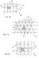
- FIG. 1A shows in a top view according to IA in FIG. 1 the patterned electrically conductive layer 40.
- the patterned electrically conductive layer is a hexagonal maze, having elongated electrically conductive elements 41 that define openings 43.
- the electrically conductive layer may alternatively be patterned in the form of a plurality of parallel lines, as shown in FIG. 1E .
- the pattern of parallel lines may be coupled to relatively wide busbars as shown in FIG. 1F .
- the pattern of the electrically conductive layer 40 comprises a plurality of regular spaced openings 43 to allow transmission of photon radiation.
- the openings are bounded by elongate conductive elements 41 extending in a plane defined by the patterned electrically conductive layer and said elongate conductive elements having in said plane a length that is at least 10 times their width.
- the conductive elements may have a height in the range of 0.001 to 10 times the width for example.
- the patterned electrically conductive layer 40 may have contact fields 44, to facilitate application of an electrical contact between the patterned electrically conductive layer 40 and an external conductor.
- the elongated electrically conductive elements 41 may have a length of about 0.5 to 5 mm, for example about 1 mm. In the embodiments shown in FIG.
- the elongate electrically conductive elements 41 extend over the full width or length of the device and may be arranged at a distance of 0.5 mm to 5 mm for example, e.g. spaced at a distance of 1 mm from each other.
- the width of the elements is about 50 ⁇ m. However, depending on the application, another value for the width may be selected for example in the interval of 1 to 500 ⁇ m.
- the elongate conductive elements have a height of a few ⁇ m.
- the patterned electrically conductive layer 40 further comprises bus bars 42.
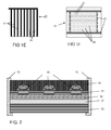
- FIG. 2 shows an alternative embodiment of the device according to the invention.
- the electrode 20 is carried out in the form of a metal foil, e.g. a steel foil having a thickness of 0.1 mm.
- the metal foil serving as the electrode also provides for a barrier against moisture and oxygen.
- the device may be sealed laterally with a sealing ring 70.
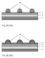
- FIG. 3A to 3F shows an embodiment of a method according to the second aspect of the invention for manufacturing an opto-electric device.
- the method is used to manufacture the opto-electrical device schematically shown in FIG. 1 and having the patterned electrically conductive layer 40 as shown in FIG. 1F .
- the embodiment of the method shown in FIG. 3A to 3F comprises a first step S1, shown in FIG. 3A , wherein an electrode 20 is provided in the form of a stainless steel foil having a thickness of about 50 ⁇ m.
- a thinner metal foil e.g. 20 ⁇ m or a thicker metal foil, e.g. 300 ⁇ m may be used.
- the device has a size of 2x2 cm.
- the stainless steel foil serving as the electrode 20 also forms a substrate for the device, and functions as a barrier against moisture and oxygen.
- the device may be provided with a separate substrate e.g. a rigid substrate in the form of a glass plate or a flexible substrate e.g.
- a polymer foil e.g. a foil from polyethylene therephtalate (PET) or polyethylene naphtalate (PEN).
- PET polyethylene therephtalate
- PEN polyethylene naphtalate
- the polymer foil may be provided with a barrier layer, e.g. comprising a sequence of inorganic sub-layers of a different type, or inorganic sublayers separated by organic planarization layers.
- a hole-injection layer 25 is provided in a second step S2 by spincoating.
- the hole injection layer is a pedot (polyethylene dioxythiophene) layer having a thickness in the range of 10 to 500 nm, here a thickness of 100 nm.
- FIG. 3C shows a third step wherein an organic opto-electric layer 30, here yellow poly(para-phenylene vinylene) derivative is deposited by spin-coating on the first electrode layer 20 provided with the hole-injection layer 25. Nevertheless other polymer or small molecule electroluminescent materials may be used for the electroluminescent layer.
- the thickness of the organic opto-electric layer 30 may be varied in the range of 50 to 200 nm. In the present case it has a thickness of about 100 nm.
- a patterned electrically conductive layer 40 is deposited on the organic opto-electric layer 30.
- the electrically conductive layer 40 patterned as shown in FIG. 1F is deposited by a printing process.
- a silver nanoparticle dispersion in an ethylene glycol/ethanol mixture was purchased from Cabot (Cabot Printing Electronics and Displays, USA).
- the silver ink contains 20 wt% of silver nanoparticles, with the particle diameter ranging from 30 to 50 nm.
- the viscosity and surface tension of the ink were 14.4 mPa.s and 31 mN m-1, respectively.
- the silver nanoparticle dispersion was applied at organic opto-electric layer 30 by inkjet printing using a piezoelectric inkjet printer of type Dimatix DMP 2800 (Dimatix-Fujifilm Inc., USA), equipped with a 10 pL cartridge (DMC-11610).
- the print head thereof contains 16 parallel squared nozzles with a diameter of 30 ⁇ m.
- the dispersion was printed using a customized wave form (average nozzle voltage 28 V, frequency of 20 kHz, meniscus set point 4 inches H2O, printing height 0.5 mm, drop spacing of 20 ⁇ m).
- the line width was set to a value of 100 ⁇ m.
- the patterned electrically conductive layer 40 was printed in the form of a series of mutually parallel lines, regularly spaced at a distance of 1 mm from each other. This printing step was carried out under atmospheric conditions.
- a second, transparent, electrode layer 50 is provided on the organic opto-electric layer 30 layer provided with the patterned electrically conductive layer 40.
- the second transparent electrode layer in this exemplary embodiment comprises a first and a second sublayer.
- the first sub-layer, closest to the organic opto-electric layer is formed by barium and has a thickness of 5 nm.
- the second sub-layer, more remote from the organic opto-electric layer is formed by ITO and has a thickness of 50 to 500 nm.
- the first sublayer may be formed of MgAg for example having a thickness of 5-40nm.
- other sublayers of other materials, such as Li, copper phthalocyanine (CuPc), LiF, Al and Ag may be used.
- CuPc copper phthalocyanine
- LiF LiF
- Al aluminum
- Ag silver
- ITO another transparent metal oxide, such as IZO, may be used for this sublayer.
- a barrier layer 60 comprising a plurality of sub-layers (not shown) is deposited on the transparent, electrode layer 50.
- the device may be laterally sealed by a sealing 70 as shown in FIGs. 2 and 6 , to prevent a lateral diffusion of moisture and/or oxygen.
- Suitable materials for use as a sealant are epoxy resins or acrylate resins filled with inorganic particles.
- a sealing may be provided by providing an extension of the barrier layers beyond the area of the functional layers between them, so that these barrier layers fully encapsulate these functional layers, as shown in FIG. 7A , or as shown in FIG. 7B , wherein a metal substrate 10 serves as the second barrier layer.
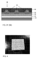
- FIG. 4 shows a photograph of the device obtained with the method described with reference to FIG. 3A to 3F .
- FIG. 5 shows a photograph of another device obtained with the method of FIG. 3A-3F .
- the substrate also a steel foil, has a size of 15 x15 cm.
- the patterned electrically conductive layer 40 is formed in a hexagonal maze structure as shown in FIG. 1A .
- the maze structure of the patterned electrically conductive layer 40 has elongated elements with a length of about 5 mm, a width of 100 ⁇ m and a height of 2 ⁇ m.
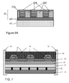
- FIG. 6 shows a further embodiment of an opto-electric device according to the second aspect of the present invention.
- the device is provided with a further shunting structure 22 in the form of a patterned electrically conductive layer that is embedded in a transparent material, as is described in patent Application EP2158176 filed by the same Applicant.
- This structure is shown in more detail in FIG. 6A .
- Reference numeral 10 denotes here a transparent substrate, such as a glass or a polymer plate.
- the further shunting structure 22 comprises a first inorganic layer 221, an organic layer 222, a second inorganic layer 223, and the patterned electrically conductive layer 224.
- the electrically conductive layer 224 may be patterned in a way as described with reference to FIGs 1A to 1F for example.
- FIG. 7 shows a still further embodiment of an opto-electric device according to the second aspect of the present invention.
- the device is further provided with an insulating layer 45 that is patterned conformaly to the pattern of the patterned electrically conductive layer 40.
- the patterned insulating layer 45 helps to prevent electrical shorts in the device, as there is no direct contact between the patterned electrically conductive layer 40 and the opto-electric layer 30.
- the patterned electrically insulating layer 45 may have lineshaped features having a width that is up to 20% larger than the width of lineshaped features of the patterned electrically conductive layer 40, so that the patterned electrically insulating layer 45 laterally extends slightly beyond the patterned electrically conductive layer 40.
- the opto-electric device of FIG. 7 has a further shunting structure 22 similar to that of FIG 6 and 6A .
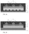
- FIG. 7A shows a still further alternative embodiment of a device according to the second aspect of the invention.
- the barrier layers 60 and 21 extend beyond the area used by the functional layers 22, 25, 30, 40, 45, 50 arranged between them. Therewith the barrier layers 21 and 60 fully encapsulate those functional layers.
- FIG. 7B shows again a further alternative embodiment of a device according to the second aspect of the invention.
- the barrier layer 60 and the metal substrate 10 also serving as a barrier layer extend beyond the area used by the functional layers 22, 25, 30, 40, 45, 50 arranged between them. Therewith the barrier layer 60 and the metal substrate 10 fully encapsulate those functional layers.
- the present invention is described in particular with reference to an electroluminescent device in the form of an OLED, the invention may also be applicable to other kinds of electroluminescent devices. Likewise the present invention is applicable to photovoltaic devices, electrochromic devices and displays.
Landscapes
- Physics & Mathematics (AREA)
- Optics & Photonics (AREA)
- Engineering & Computer Science (AREA)
- Manufacturing & Machinery (AREA)
- Electroluminescent Light Sources (AREA)
- Photovoltaic Devices (AREA)
Priority Applications (7)
| Application Number | Priority Date | Filing Date | Title |
|---|---|---|---|
| EP20100166379 EP2398086A1 (en) | 2010-06-17 | 2010-06-17 | Opto-electric device and method of manufacturing thereof |
| US13/704,644 US8963193B2 (en) | 2010-06-17 | 2011-06-17 | Opto-electric device and method of manufacturing thereof |
| KR1020137001352A KR101811476B1 (ko) | 2010-06-17 | 2011-06-17 | 광전 장치 및 그 제조 방법 |
| JP2013515287A JP5739989B2 (ja) | 2010-06-17 | 2011-06-17 | 光電気デバイスおよびその製造方法 |
| CN201180035247.1A CN103038912B (zh) | 2010-06-17 | 2011-06-17 | 光电器件及其制造方法 |
| PCT/NL2011/050438 WO2011159160A1 (en) | 2010-06-17 | 2011-06-17 | Opto-electric device and method of manufacturing thereof |
| EP11728434.9A EP2583327B1 (en) | 2010-06-17 | 2011-06-17 | OLED lighting device and method of manufacturing the same |
Applications Claiming Priority (1)
| Application Number | Priority Date | Filing Date | Title |
|---|---|---|---|
| EP20100166379 EP2398086A1 (en) | 2010-06-17 | 2010-06-17 | Opto-electric device and method of manufacturing thereof |
Publications (1)
| Publication Number | Publication Date |
|---|---|
| EP2398086A1 true EP2398086A1 (en) | 2011-12-21 |
Family
ID=43086316
Family Applications (2)
| Application Number | Title | Priority Date | Filing Date |
|---|---|---|---|
| EP20100166379 Withdrawn EP2398086A1 (en) | 2010-06-17 | 2010-06-17 | Opto-electric device and method of manufacturing thereof |
| EP11728434.9A Not-in-force EP2583327B1 (en) | 2010-06-17 | 2011-06-17 | OLED lighting device and method of manufacturing the same |
Family Applications After (1)
| Application Number | Title | Priority Date | Filing Date |
|---|---|---|---|
| EP11728434.9A Not-in-force EP2583327B1 (en) | 2010-06-17 | 2011-06-17 | OLED lighting device and method of manufacturing the same |
Country Status (6)
| Country | Link |
|---|---|
| US (1) | US8963193B2 (enExample) |
| EP (2) | EP2398086A1 (enExample) |
| JP (1) | JP5739989B2 (enExample) |
| KR (1) | KR101811476B1 (enExample) |
| CN (1) | CN103038912B (enExample) |
| WO (1) | WO2011159160A1 (enExample) |
Cited By (6)
| Publication number | Priority date | Publication date | Assignee | Title |
|---|---|---|---|---|
| CN103999250A (zh) * | 2012-05-31 | 2014-08-20 | 株式会社Lg化学 | 有机发光器件及其制备方法 |
| US9606411B2 (en) | 2012-08-08 | 2017-03-28 | Kinestral Technologies, Inc. | Electrochromic multi-layer devices with composite electrically conductive layers |
| US9606410B2 (en) | 2012-08-08 | 2017-03-28 | Kinestral Technologies, Inc. | Electrochromic multi-layer devices with composite current modulating structure |
| US9958751B2 (en) | 2012-08-08 | 2018-05-01 | Kinestral Technologies, Inc. | Electrochromic multi-layer devices with current modulating structure |
| EP4395514A1 (de) * | 2022-12-31 | 2024-07-03 | Fredy Doll Beteiligungs-GmbH | Verfahren zum aufbringen einer beschichtung auf ein fahrzeug oder ein fahrzeugteil |
| US12089435B2 (en) | 2018-10-11 | 2024-09-10 | The Boeing Company | Multifunctional composite panels and methods for the same |
Families Citing this family (23)
| Publication number | Priority date | Publication date | Assignee | Title |
|---|---|---|---|---|
| DE102009054555A1 (de) * | 2009-12-11 | 2011-06-16 | Osram Opto Semiconductors Gmbh | Optoelektronischer Halbleiterchip und Verfahren zum Herstellen eines optoelektronischen Halbleiterchips |
| EP2398086A1 (en) * | 2010-06-17 | 2011-12-21 | Nederlandse Organisatie voor toegepast -natuurwetenschappelijk onderzoek TNO | Opto-electric device and method of manufacturing thereof |
| JP5829070B2 (ja) * | 2010-07-26 | 2015-12-09 | 株式会社半導体エネルギー研究所 | 発光装置、照明装置、及び発光装置の作製方法 |
| US8717658B2 (en) | 2011-02-09 | 2014-05-06 | Kinestral Technologies, Inc. | Electrochromic multi-layer devices with spatially coordinated switching |
| JP5991627B2 (ja) * | 2011-05-20 | 2016-09-14 | パナソニックIpマネジメント株式会社 | 有機エレクトロルミネッセンス素子 |
| US9024306B2 (en) * | 2011-05-20 | 2015-05-05 | Panasonic Intellectual Property Management Co., Ltd. | Organic electroluminescence element |
| TWI547208B (zh) * | 2012-03-19 | 2016-08-21 | 友達光電股份有限公司 | 有機電致發光裝置 |
| TWI543395B (zh) * | 2013-04-01 | 2016-07-21 | 中國砂輪企業股份有限公司 | 圖案化光電基板及其製作方法 |
| DE102014018277A1 (de) * | 2014-12-12 | 2016-06-16 | Tesat-Spacecom Gmbh & Co. Kg | Verfahren zum Hestellen einer Hochspannungsisolierung von elektrischen Komponenten |
| EP3034548A1 (en) * | 2014-12-18 | 2016-06-22 | Nederlandse Organisatie voor toegepast- natuurwetenschappelijk onderzoek TNO | Barrier film laminate comprising submicron getter particles and electronic device comprising such a laminate |
| JP2017069030A (ja) * | 2015-09-30 | 2017-04-06 | 住友化学株式会社 | 有機el素子の製造方法 |
| US9793317B1 (en) * | 2016-04-09 | 2017-10-17 | Face International Corporation | Devices and systems incorporating energy harvesting components/devices as autonomous energy sources and as energy supplementation, and methods for producing devices and systems incorporating energy harvesting components/devices |
| GB2549938A (en) | 2016-04-29 | 2017-11-08 | Sumitomo Chemical Co | Electroluminescence device |
| NL2017872B1 (en) * | 2016-11-25 | 2018-06-08 | Stichting Energieonderzoek Centrum Nederland | Photovoltaic cell with passivating contact |
| CN109974305B (zh) * | 2017-12-28 | 2022-09-16 | 武汉海尔热水器有限公司 | 一种外壳及电热水器 |
| US10718886B1 (en) * | 2018-05-23 | 2020-07-21 | Facebook Technologies, Llc | Optical substrate and transparent routing of light sources |
| CN109215509A (zh) * | 2018-08-28 | 2019-01-15 | 上海幂方电子科技有限公司 | 一种可穿戴显示设备 |
| US11380863B2 (en) * | 2019-03-19 | 2022-07-05 | Nanosys, Inc. | Flexible electroluminescent devices |
| WO2021084598A1 (ja) * | 2019-10-29 | 2021-05-06 | シャープ株式会社 | 発光素子 |
| JPWO2022154009A1 (enExample) * | 2021-01-15 | 2022-07-21 | ||
| CN113959605B (zh) * | 2021-10-19 | 2024-08-13 | 广州碳思科技有限公司 | 一种应力传感器及应力传感装置 |
| WO2025080301A2 (en) * | 2023-04-19 | 2025-04-17 | Virginia Tech Intellectual Properties, Inc. | Chip-integrated nanolaminate nano-optoelectrode arrays for nonlinear optical voltage sensing |
| WO2025193250A1 (en) * | 2023-09-01 | 2025-09-18 | Virginia Tech Intellectual Properties, Inc. | Chip-integrated nanolaminate nano-optoelectrode arrays for interfacial electrochemical reaction monitoring |
Citations (15)
| Publication number | Priority date | Publication date | Assignee | Title |
|---|---|---|---|---|
| EP0331997A1 (en) * | 1988-03-05 | 1989-09-13 | Stanley Electric Co., Ltd. | Elongated electroluminescence element and manufacturing method thereof |
| EP0845924A2 (en) * | 1996-11-29 | 1998-06-03 | Idemitsu Kosan Company Limited | Organic electroluminescent device |
| WO2000070655A2 (en) | 1999-05-13 | 2000-11-23 | The Trustees Of Princeton University | Very high efficiency organic light emitting devices based on electrophosphorescence |
| WO2001041512A1 (en) | 1999-12-01 | 2001-06-07 | The Trustees Of Princeton University | Complexes of form l2mx as phosphorescent dopants for organic leds |
| US6303238B1 (en) | 1997-12-01 | 2001-10-16 | The Trustees Of Princeton University | OLEDs doped with phosphorescent compounds |
| WO2003008424A1 (en) | 2001-07-18 | 2003-01-30 | E.I. Du Pont De Nemours And Company | Luminescent lanthanide complexes with imine ligands and devices made with such complexes |
| WO2003040257A1 (en) | 2001-11-07 | 2003-05-15 | E. I. Du Pont De Nemours And Company | Electroluminescent platinum compounds and devices made with such compounds |
| WO2003063555A1 (en) | 2001-12-26 | 2003-07-31 | E. I. Du Pont De Nemours And Company | Electroluminescent iridium compounds wiht fluorinated phenylpyridines, phenylpyrimidines, and phenylquinolines and devices made with such compounds |
| WO2003091688A2 (en) | 2001-07-05 | 2003-11-06 | E.I. Du Pont De Nemours And Company | Photoactive lanthanide complexes with phosphine oxides, phosphine oxide-sulfides, pyridine n-oxides, and phosphine oxide-pyridine n-oxides, and devices made with such complexes |
| US6670645B2 (en) | 2000-06-30 | 2003-12-30 | E. I. Du Pont De Nemours And Company | Electroluminescent iridium compounds with fluorinated phenylpyridines, phenylpyrimidines, and phenylquinolines and devices made with such compounds |
| WO2004016710A1 (en) | 2002-08-15 | 2004-02-26 | E.I. Du Pont De Nemours And Company | Compounds comprising phosphorus-containing metal complexes |
| US20060279202A1 (en) * | 2005-05-27 | 2006-12-14 | Fuji Photo Film Co., Ltd. | Vapor deposition mask, organic electroluminescent display device, and manufacturing method therefor |
| WO2007036850A2 (en) | 2005-09-28 | 2007-04-05 | Koninklijke Philips Electronics N.V. | A large area organic diode device and a method of manufacturing it |
| US20070085471A1 (en) * | 2005-10-18 | 2007-04-19 | Eastman Kodak Company | OLED device having improved power distribution |
| EP2158176A1 (en) | 2007-06-27 | 2010-03-03 | Arkema, Inc. | Two step process for the manufacture of hydrofluoroolefins |
Family Cites Families (21)
| Publication number | Priority date | Publication date | Assignee | Title |
|---|---|---|---|---|
| US7022910B2 (en) | 2002-03-29 | 2006-04-04 | Konarka Technologies, Inc. | Photovoltaic cells utilizing mesh electrodes |
| US6605483B2 (en) | 2000-04-27 | 2003-08-12 | Add-Vision, Inc. | Screen printing light-emitting polymer patterned devices |
| AU2002361859A1 (en) | 2001-12-20 | 2003-07-09 | Add-Vision, Inc. | Screen printable electrode for organic light emitting device |
| DE60227696D1 (de) | 2001-12-20 | 2008-08-28 | Add Vision Inc | Siebdruckfähige, elektrolumineszierende polymertinte |
| US6812637B2 (en) | 2003-03-13 | 2004-11-02 | Eastman Kodak Company | OLED display with auxiliary electrode |
| JP4969041B2 (ja) * | 2004-01-26 | 2012-07-04 | 株式会社半導体エネルギー研究所 | 表示装置の作製方法 |
| DE102004013449B3 (de) | 2004-03-11 | 2005-12-29 | Samsung SDI Co., Ltd., Suwon | OLED-Display mit Elektroden hoher Leitfähigkeit und Verfahren zu dessen Herstellung |
| JP4121514B2 (ja) * | 2004-07-22 | 2008-07-23 | シャープ株式会社 | 有機発光素子、及び、それを備えた表示装置 |
| JP4923401B2 (ja) | 2004-11-16 | 2012-04-25 | 大日本印刷株式会社 | 発光表示パネル及びその製造方法 |
| US7982211B2 (en) | 2005-06-30 | 2011-07-19 | Koninklijke Philips Electronics N.V. | Organic based device and method for manufacture thereof |
| JP4736676B2 (ja) * | 2005-09-29 | 2011-07-27 | 凸版印刷株式会社 | アクティブマトリクス駆動型有機エレクトロルミネッセンス表示装置 |
| US20070077349A1 (en) | 2005-09-30 | 2007-04-05 | Eastman Kodak Company | Patterning OLED device electrodes and optical material |
| JP2007213999A (ja) * | 2006-02-10 | 2007-08-23 | Seiko Epson Corp | 有機el装置の製造方法及び有機el装置 |
| JP2007227129A (ja) | 2006-02-23 | 2007-09-06 | Seiko Epson Corp | 有機el装置及び有機el装置の製造方法 |
| JP4702136B2 (ja) * | 2006-03-28 | 2011-06-15 | セイコーエプソン株式会社 | 発光装置および電子機器 |
| DE102006016373A1 (de) | 2006-04-05 | 2007-10-11 | Merck Patent Gmbh | Großflächige OLED's mit homogener Lichtemission |
| WO2009001241A1 (en) | 2007-06-25 | 2008-12-31 | Koninklijke Philips Electronics N.V. | Organic functional device and method of manufacturing same |
| CN101730938B (zh) | 2007-07-04 | 2012-10-10 | 皇家飞利浦电子股份有限公司 | 在衬底上形成图案化层的方法 |
| US8563967B2 (en) | 2007-07-11 | 2013-10-22 | Koninklijke Philips N.V. | Organic functional device and manufacturing method therefor |
| EP2398086A1 (en) * | 2010-06-17 | 2011-12-21 | Nederlandse Organisatie voor toegepast -natuurwetenschappelijk onderzoek TNO | Opto-electric device and method of manufacturing thereof |
| US9024306B2 (en) * | 2011-05-20 | 2015-05-05 | Panasonic Intellectual Property Management Co., Ltd. | Organic electroluminescence element |
-
2010
- 2010-06-17 EP EP20100166379 patent/EP2398086A1/en not_active Withdrawn
-
2011
- 2011-06-17 CN CN201180035247.1A patent/CN103038912B/zh not_active Expired - Fee Related
- 2011-06-17 WO PCT/NL2011/050438 patent/WO2011159160A1/en not_active Ceased
- 2011-06-17 JP JP2013515287A patent/JP5739989B2/ja not_active Expired - Fee Related
- 2011-06-17 US US13/704,644 patent/US8963193B2/en not_active Expired - Fee Related
- 2011-06-17 EP EP11728434.9A patent/EP2583327B1/en not_active Not-in-force
- 2011-06-17 KR KR1020137001352A patent/KR101811476B1/ko not_active Expired - Fee Related
Patent Citations (15)
| Publication number | Priority date | Publication date | Assignee | Title |
|---|---|---|---|---|
| EP0331997A1 (en) * | 1988-03-05 | 1989-09-13 | Stanley Electric Co., Ltd. | Elongated electroluminescence element and manufacturing method thereof |
| EP0845924A2 (en) * | 1996-11-29 | 1998-06-03 | Idemitsu Kosan Company Limited | Organic electroluminescent device |
| US6303238B1 (en) | 1997-12-01 | 2001-10-16 | The Trustees Of Princeton University | OLEDs doped with phosphorescent compounds |
| WO2000070655A2 (en) | 1999-05-13 | 2000-11-23 | The Trustees Of Princeton University | Very high efficiency organic light emitting devices based on electrophosphorescence |
| WO2001041512A1 (en) | 1999-12-01 | 2001-06-07 | The Trustees Of Princeton University | Complexes of form l2mx as phosphorescent dopants for organic leds |
| US6670645B2 (en) | 2000-06-30 | 2003-12-30 | E. I. Du Pont De Nemours And Company | Electroluminescent iridium compounds with fluorinated phenylpyridines, phenylpyrimidines, and phenylquinolines and devices made with such compounds |
| WO2003091688A2 (en) | 2001-07-05 | 2003-11-06 | E.I. Du Pont De Nemours And Company | Photoactive lanthanide complexes with phosphine oxides, phosphine oxide-sulfides, pyridine n-oxides, and phosphine oxide-pyridine n-oxides, and devices made with such complexes |
| WO2003008424A1 (en) | 2001-07-18 | 2003-01-30 | E.I. Du Pont De Nemours And Company | Luminescent lanthanide complexes with imine ligands and devices made with such complexes |
| WO2003040257A1 (en) | 2001-11-07 | 2003-05-15 | E. I. Du Pont De Nemours And Company | Electroluminescent platinum compounds and devices made with such compounds |
| WO2003063555A1 (en) | 2001-12-26 | 2003-07-31 | E. I. Du Pont De Nemours And Company | Electroluminescent iridium compounds wiht fluorinated phenylpyridines, phenylpyrimidines, and phenylquinolines and devices made with such compounds |
| WO2004016710A1 (en) | 2002-08-15 | 2004-02-26 | E.I. Du Pont De Nemours And Company | Compounds comprising phosphorus-containing metal complexes |
| US20060279202A1 (en) * | 2005-05-27 | 2006-12-14 | Fuji Photo Film Co., Ltd. | Vapor deposition mask, organic electroluminescent display device, and manufacturing method therefor |
| WO2007036850A2 (en) | 2005-09-28 | 2007-04-05 | Koninklijke Philips Electronics N.V. | A large area organic diode device and a method of manufacturing it |
| US20070085471A1 (en) * | 2005-10-18 | 2007-04-19 | Eastman Kodak Company | OLED device having improved power distribution |
| EP2158176A1 (en) | 2007-06-27 | 2010-03-03 | Arkema, Inc. | Two step process for the manufacture of hydrofluoroolefins |
Non-Patent Citations (1)
| Title |
|---|
| "Flexible light-emitting diodes made from soluble conducting polymer", NATURE, vol. 357, 11 June 1992 (1992-06-11), pages 477479 |
Cited By (8)
| Publication number | Priority date | Publication date | Assignee | Title |
|---|---|---|---|---|
| CN103999250A (zh) * | 2012-05-31 | 2014-08-20 | 株式会社Lg化学 | 有机发光器件及其制备方法 |
| EP2752909A4 (en) * | 2012-05-31 | 2015-07-08 | Lg Chemical Ltd | ORGANIC LIGHT-EMITTING DEVICE AND METHOD FOR THE PRODUCTION THEREOF |
| US9444057B2 (en) | 2012-05-31 | 2016-09-13 | Lg Display Co., Ltd. | Organic light-emitting device and method for manufacturing same |
| US9606411B2 (en) | 2012-08-08 | 2017-03-28 | Kinestral Technologies, Inc. | Electrochromic multi-layer devices with composite electrically conductive layers |
| US9606410B2 (en) | 2012-08-08 | 2017-03-28 | Kinestral Technologies, Inc. | Electrochromic multi-layer devices with composite current modulating structure |
| US9958751B2 (en) | 2012-08-08 | 2018-05-01 | Kinestral Technologies, Inc. | Electrochromic multi-layer devices with current modulating structure |
| US12089435B2 (en) | 2018-10-11 | 2024-09-10 | The Boeing Company | Multifunctional composite panels and methods for the same |
| EP4395514A1 (de) * | 2022-12-31 | 2024-07-03 | Fredy Doll Beteiligungs-GmbH | Verfahren zum aufbringen einer beschichtung auf ein fahrzeug oder ein fahrzeugteil |
Also Published As
| Publication number | Publication date |
|---|---|
| CN103038912B (zh) | 2016-03-16 |
| CN103038912A (zh) | 2013-04-10 |
| KR101811476B1 (ko) | 2017-12-26 |
| JP5739989B2 (ja) | 2015-06-24 |
| US8963193B2 (en) | 2015-02-24 |
| WO2011159160A1 (en) | 2011-12-22 |
| EP2583327A1 (en) | 2013-04-24 |
| EP2583327B1 (en) | 2018-08-08 |
| US20130214255A1 (en) | 2013-08-22 |
| KR20130097138A (ko) | 2013-09-02 |
| JP2013532365A (ja) | 2013-08-15 |
Similar Documents
| Publication | Publication Date | Title |
|---|---|---|
| EP2583327B1 (en) | OLED lighting device and method of manufacturing the same | |
| US20090101870A1 (en) | Electron transport bi-layers and devices made with such bi-layers | |
| EP2549560B1 (en) | Organic electronic device and method of manufacturing the same | |
| WO2010065505A2 (en) | Anode for an organic electronic device | |
| US20110223340A1 (en) | Electro-form nozzle apparatus and method for solution coating | |
| US8907353B2 (en) | Process for forming an electroactive layer | |
| WO2010079330A1 (en) | Interlayer formulation for flat films | |
| KR20110134452A (ko) | 전기활성 층을 형성하기 위한 방법 | |
| WO2010079331A1 (en) | Interlayer formulation for flat films | |
| US20110193066A1 (en) | Current limiting element for pixels in electronic devices | |
| KR20110134461A (ko) | 전기활성 층을 형성하기 위한 방법 | |
| US20130248842A1 (en) | Organic electronic device with composite electrode | |
| US20070020395A1 (en) | Process for making an electronic device | |
| EP2430680A2 (en) | Organic electronic device with electron tunneling layer | |
| JP6015087B2 (ja) | 有機エレクトロルミネッセンス素子の製造方法 | |
| JP6255796B2 (ja) | 透明電極の製造方法、透明電極、及びそれを備えた有機エレクトロルミネッセンス素子の製造方法、有機エレクトロルミネッセンス素子 | |
| EP2373426A1 (en) | Electro-form nozzle apparatus and method for solution coating | |
| US20120139437A1 (en) | Electrical drive scheme for pixels in electronic devices | |
| EP2086034A1 (en) | Electronic device and method of manufacturing thereof | |
| JP2017098185A (ja) | 透明電極、透明電極を備えた有機エレクトロルミネッセンス素子、透明電極の製造方法及び有機エレクトロルミネッセンス素子の製造方法 | |
| JP2015064958A (ja) | 透明電極、及びそれを備えた有機エレクトロルミネッセンス素子 |
Legal Events
| Date | Code | Title | Description |
|---|---|---|---|
| AK | Designated contracting states |
Kind code of ref document: A1 Designated state(s): AL AT BE BG CH CY CZ DE DK EE ES FI FR GB GR HR HU IE IS IT LI LT LU LV MC MK MT NL NO PL PT RO SE SI SK SM TR |
|
| AX | Request for extension of the european patent |
Extension state: BA ME RS |
|
| PUAI | Public reference made under article 153(3) epc to a published international application that has entered the european phase |
Free format text: ORIGINAL CODE: 0009012 |
|
| RIN1 | Information on inventor provided before grant (corrected) |
Inventor name: WILSON, JOANNE SARAH Inventor name: HERMES, DOROTHEE CHRISTINE |
|
| STAA | Information on the status of an ep patent application or granted ep patent |
Free format text: STATUS: THE APPLICATION IS DEEMED TO BE WITHDRAWN |
|
| 18D | Application deemed to be withdrawn |
Effective date: 20120622 |